WO2011102547A1 - 電力用半導体素子 - Google Patents
電力用半導体素子 Download PDFInfo
- Publication number
- WO2011102547A1 WO2011102547A1 PCT/JP2011/054215 JP2011054215W WO2011102547A1 WO 2011102547 A1 WO2011102547 A1 WO 2011102547A1 JP 2011054215 W JP2011054215 W JP 2011054215W WO 2011102547 A1 WO2011102547 A1 WO 2011102547A1
- Authority
- WO
- WIPO (PCT)
- Prior art keywords
- semiconductor element
- electrode
- connection terminal
- power semiconductor
- temperature
- Prior art date
- Legal status (The legal status is an assumption and is not a legal conclusion. Google has not performed a legal analysis and makes no representation as to the accuracy of the status listed.)
- Ceased
Links
Images
Classifications
-
- H—ELECTRICITY
- H10—SEMICONDUCTOR DEVICES; ELECTRIC SOLID-STATE DEVICES NOT OTHERWISE PROVIDED FOR
- H10W—GENERIC PACKAGES, INTERCONNECTIONS, CONNECTORS OR OTHER CONSTRUCTIONAL DETAILS OF DEVICES COVERED BY CLASS H10
- H10W72/00—Interconnections or connectors in packages
- H10W72/30—Die-attach connectors
-
- H—ELECTRICITY
- H10—SEMICONDUCTOR DEVICES; ELECTRIC SOLID-STATE DEVICES NOT OTHERWISE PROVIDED FOR
- H10W—GENERIC PACKAGES, INTERCONNECTIONS, CONNECTORS OR OTHER CONSTRUCTIONAL DETAILS OF DEVICES COVERED BY CLASS H10
- H10W72/00—Interconnections or connectors in packages
- H10W72/90—Bond pads, in general
-
- H—ELECTRICITY
- H10—SEMICONDUCTOR DEVICES; ELECTRIC SOLID-STATE DEVICES NOT OTHERWISE PROVIDED FOR
- H10W—GENERIC PACKAGES, INTERCONNECTIONS, CONNECTORS OR OTHER CONSTRUCTIONAL DETAILS OF DEVICES COVERED BY CLASS H10
- H10W72/00—Interconnections or connectors in packages
- H10W72/071—Connecting or disconnecting
- H10W72/073—Connecting or disconnecting of die-attach connectors
- H10W72/07331—Connecting techniques
- H10W72/07332—Compression bonding, e.g. thermocompression bonding
- H10W72/07333—Ultrasonic bonding, e.g. thermosonic bonding
-
- H—ELECTRICITY
- H10—SEMICONDUCTOR DEVICES; ELECTRIC SOLID-STATE DEVICES NOT OTHERWISE PROVIDED FOR
- H10W—GENERIC PACKAGES, INTERCONNECTIONS, CONNECTORS OR OTHER CONSTRUCTIONAL DETAILS OF DEVICES COVERED BY CLASS H10
- H10W72/00—Interconnections or connectors in packages
- H10W72/071—Connecting or disconnecting
- H10W72/075—Connecting or disconnecting of bond wires
- H10W72/07531—Techniques
- H10W72/07532—Compression bonding, e.g. thermocompression bonding
- H10W72/07533—Ultrasonic bonding, e.g. thermosonic bonding
-
- H—ELECTRICITY
- H10—SEMICONDUCTOR DEVICES; ELECTRIC SOLID-STATE DEVICES NOT OTHERWISE PROVIDED FOR
- H10W—GENERIC PACKAGES, INTERCONNECTIONS, CONNECTORS OR OTHER CONSTRUCTIONAL DETAILS OF DEVICES COVERED BY CLASS H10
- H10W72/00—Interconnections or connectors in packages
- H10W72/30—Die-attach connectors
- H10W72/351—Materials of die-attach connectors
- H10W72/352—Materials of die-attach connectors comprising metals or metalloids, e.g. solders
-
- H—ELECTRICITY
- H10—SEMICONDUCTOR DEVICES; ELECTRIC SOLID-STATE DEVICES NOT OTHERWISE PROVIDED FOR
- H10W—GENERIC PACKAGES, INTERCONNECTIONS, CONNECTORS OR OTHER CONSTRUCTIONAL DETAILS OF DEVICES COVERED BY CLASS H10
- H10W72/00—Interconnections or connectors in packages
- H10W72/50—Bond wires
- H10W72/521—Structures or relative sizes of bond wires
- H10W72/522—Multilayered bond wires, e.g. having a coating concentric around a core
-
- H—ELECTRICITY
- H10—SEMICONDUCTOR DEVICES; ELECTRIC SOLID-STATE DEVICES NOT OTHERWISE PROVIDED FOR
- H10W—GENERIC PACKAGES, INTERCONNECTIONS, CONNECTORS OR OTHER CONSTRUCTIONAL DETAILS OF DEVICES COVERED BY CLASS H10
- H10W72/00—Interconnections or connectors in packages
- H10W72/50—Bond wires
- H10W72/531—Shapes of wire connectors
- H10W72/5363—Shapes of wire connectors the connected ends being wedge-shaped
-
- H—ELECTRICITY
- H10—SEMICONDUCTOR DEVICES; ELECTRIC SOLID-STATE DEVICES NOT OTHERWISE PROVIDED FOR
- H10W—GENERIC PACKAGES, INTERCONNECTIONS, CONNECTORS OR OTHER CONSTRUCTIONAL DETAILS OF DEVICES COVERED BY CLASS H10
- H10W72/00—Interconnections or connectors in packages
- H10W72/50—Bond wires
- H10W72/541—Dispositions of bond wires
- H10W72/5434—Dispositions of bond wires the connected ends being on auxiliary connecting means on bond pads, e.g. on other bond wires
-
- H—ELECTRICITY
- H10—SEMICONDUCTOR DEVICES; ELECTRIC SOLID-STATE DEVICES NOT OTHERWISE PROVIDED FOR
- H10W—GENERIC PACKAGES, INTERCONNECTIONS, CONNECTORS OR OTHER CONSTRUCTIONAL DETAILS OF DEVICES COVERED BY CLASS H10
- H10W72/00—Interconnections or connectors in packages
- H10W72/50—Bond wires
- H10W72/551—Materials of bond wires
- H10W72/552—Materials of bond wires comprising metals or metalloids, e.g. silver
-
- H—ELECTRICITY
- H10—SEMICONDUCTOR DEVICES; ELECTRIC SOLID-STATE DEVICES NOT OTHERWISE PROVIDED FOR
- H10W—GENERIC PACKAGES, INTERCONNECTIONS, CONNECTORS OR OTHER CONSTRUCTIONAL DETAILS OF DEVICES COVERED BY CLASS H10
- H10W72/00—Interconnections or connectors in packages
- H10W72/50—Bond wires
- H10W72/551—Materials of bond wires
- H10W72/552—Materials of bond wires comprising metals or metalloids, e.g. silver
- H10W72/5522—Materials of bond wires comprising metals or metalloids, e.g. silver comprising gold [Au]
-
- H—ELECTRICITY
- H10—SEMICONDUCTOR DEVICES; ELECTRIC SOLID-STATE DEVICES NOT OTHERWISE PROVIDED FOR
- H10W—GENERIC PACKAGES, INTERCONNECTIONS, CONNECTORS OR OTHER CONSTRUCTIONAL DETAILS OF DEVICES COVERED BY CLASS H10
- H10W72/00—Interconnections or connectors in packages
- H10W72/50—Bond wires
- H10W72/551—Materials of bond wires
- H10W72/552—Materials of bond wires comprising metals or metalloids, e.g. silver
- H10W72/5524—Materials of bond wires comprising metals or metalloids, e.g. silver comprising aluminium [Al]
-
- H—ELECTRICITY
- H10—SEMICONDUCTOR DEVICES; ELECTRIC SOLID-STATE DEVICES NOT OTHERWISE PROVIDED FOR
- H10W—GENERIC PACKAGES, INTERCONNECTIONS, CONNECTORS OR OTHER CONSTRUCTIONAL DETAILS OF DEVICES COVERED BY CLASS H10
- H10W72/00—Interconnections or connectors in packages
- H10W72/50—Bond wires
- H10W72/551—Materials of bond wires
- H10W72/552—Materials of bond wires comprising metals or metalloids, e.g. silver
- H10W72/5525—Materials of bond wires comprising metals or metalloids, e.g. silver comprising copper [Cu]
-
- H—ELECTRICITY
- H10—SEMICONDUCTOR DEVICES; ELECTRIC SOLID-STATE DEVICES NOT OTHERWISE PROVIDED FOR
- H10W—GENERIC PACKAGES, INTERCONNECTIONS, CONNECTORS OR OTHER CONSTRUCTIONAL DETAILS OF DEVICES COVERED BY CLASS H10
- H10W72/00—Interconnections or connectors in packages
- H10W72/50—Bond wires
- H10W72/551—Materials of bond wires
- H10W72/555—Materials of bond wires of outermost layers of multilayered bond wires, e.g. material of a coating
-
- H—ELECTRICITY
- H10—SEMICONDUCTOR DEVICES; ELECTRIC SOLID-STATE DEVICES NOT OTHERWISE PROVIDED FOR
- H10W—GENERIC PACKAGES, INTERCONNECTIONS, CONNECTORS OR OTHER CONSTRUCTIONAL DETAILS OF DEVICES COVERED BY CLASS H10
- H10W72/00—Interconnections or connectors in packages
- H10W72/50—Bond wires
- H10W72/59—Bond pads specially adapted therefor
-
- H—ELECTRICITY
- H10—SEMICONDUCTOR DEVICES; ELECTRIC SOLID-STATE DEVICES NOT OTHERWISE PROVIDED FOR
- H10W—GENERIC PACKAGES, INTERCONNECTIONS, CONNECTORS OR OTHER CONSTRUCTIONAL DETAILS OF DEVICES COVERED BY CLASS H10
- H10W72/00—Interconnections or connectors in packages
- H10W72/851—Dispositions of multiple connectors or interconnections
- H10W72/874—On different surfaces
- H10W72/884—Die-attach connectors and bond wires
-
- H—ELECTRICITY
- H10—SEMICONDUCTOR DEVICES; ELECTRIC SOLID-STATE DEVICES NOT OTHERWISE PROVIDED FOR
- H10W—GENERIC PACKAGES, INTERCONNECTIONS, CONNECTORS OR OTHER CONSTRUCTIONAL DETAILS OF DEVICES COVERED BY CLASS H10
- H10W90/00—Package configurations
- H10W90/701—Package configurations characterised by the relative positions of pads or connectors relative to package parts
- H10W90/731—Package configurations characterised by the relative positions of pads or connectors relative to package parts of die-attach connectors
- H10W90/734—Package configurations characterised by the relative positions of pads or connectors relative to package parts of die-attach connectors between a chip and a stacked insulating package substrate, interposer or RDL
Definitions
- the present invention relates to a power semiconductor device that can be used in a high temperature environment.
- diodes, transistors, MOSFETs, IGBTs and the like are employed as elements for power conversion. These elements are generally formed of a silicon semiconductor material.
- a semiconductor chip having a predetermined function is obtained by dicing a silicon semiconductor material that has been subjected to various treatments by an element manufacturing process.
- a semiconductor chip is assembled as an element or module by joining an electrode formed on the surface of the semiconductor chip to a wire (connection line) connected to an electrode for connecting the other end to the outside via solder.
- the solder used for joining the electrode formed on the surface of the semiconductor chip and the wire is generally Sn / Pb-based.
- the melting point of Sn / Pb solder is about 180 ° C.
- a semiconductor element in which Sn / Pb solder is used for bonding between the electrode formed on the surface and the wire is generally used at a temperature of about 150 ° C. or lower.
- a heat cycle destruction mode is also known in a semiconductor element in which solder is used.
- the heat cycle failure mode is a failure mode that occurs due to repeated energization and non-energization even when the melting temperature of the solder is not reached.
- Patent Document 1 discloses a technique that uses two types of solder having different melting points in order to join a connection terminal and a semiconductor element. A high melting point solder is used to secure the solder thickness, and the high melting point solder is coated with a low melting point solder.
- Patent Document 2 discloses a problem in a power semiconductor module in which a silicon semiconductor chip and an aluminum wire are used. Silicon chips and aluminum wires have a large difference in linear expansion rate.
- produces in the joining interface between a wire and a pad (electrode).
- the wire may peel off in a short time.
- produces in the aluminum wire junction part joined to the pad by ultrasonic wire bonding, specifically, the tensile stress which generate
- a technique for performing geometric processing such as forming a groove in a pad is disclosed.
- Patent Document 3 discloses a composite metal wire for an electronic wire used inside a semiconductor device or electronic equipment.
- This composite metal wire for electronic wires makes it possible to ensure the strength of the ultrafine wire by covering the core of tungsten (W) with a copper (Cu) coating layer.
- a wide band gap semiconductor having a high intrinsic region temperature that functions as a semiconductor, capable of operating at a high temperature, and having a high saturation drift velocity and a high breakdown electric field.
- SiC silicon carbide
- GaN gallium nitride
- diamond For wide band gap semiconductors, an operation experiment at a high temperature of 250 ° C. to 600 ° C.
- Non-patent Document 2 By using an element formed of a wide band gap semiconductor, the element can be operated at a high temperature.
- an element formed of a wide band gap semiconductor can be stably operated by a simple cooling device such as air cooling in an environment exposed to high temperatures such as outdoors or in an automobile.
- wide band gap semiconductors have a high current density, or operate at high frequency, so that even when the temperature of the element is high, the maximum operating temperature can be given flexibility, and so on, With no advantage.
- a unipolar device such as a Schottky barrier diode and a MOSFET can be used in a high-voltage high-frequency switching circuit.
- JP 2006-339174 A JP-A-10-199923 JP-A-10-130882
- solder cannot be used as a bonding member for bonding the wide band gap semiconductor material and the connection terminal.
- the melting point of generally used solder is about 180 ° C., and this temperature is lower than the operable temperature of an element formed of a wide band gap semiconductor material.
- the solder is softened at a temperature of 150 ° C. or higher, and electrical bonding cannot be maintained.
- the material system having appropriate characteristics as solder is 260 ° C. or lower. For this reason, there is no solder that can maintain electrical bonding at a temperature of 260 ° C.
- the linear expansion coefficient of aluminum generally used as a bonding wire for power devices is 23 ⁇ 10 ⁇ 6 / K
- the linear expansion coefficient of copper is 16.8 ⁇ 10 ⁇ 6 / K
- the linear expansion coefficient of gold is The coefficient is 14.3 ⁇ 10 ⁇ 6 / K.
- the current mainstream silicon semiconductor material has a linear expansion coefficient of 2.4 ⁇ 10 ⁇ 6 / K.
- the silicon semiconductor material and the wire are formed in a temperature range in which the conventional silicon semiconductor material can be used by appropriately forming the geometric structure of the pad that forms the crimped joint portion of the aluminum wire. The problem caused by the difference of linear expansion coefficient between and was avoided.
- Patent Document 3 discloses a composite metal wire for electronic wires having tungsten as a core material and copper as a coating layer.
- Patent Document 3 does not describe any specific example of joining semiconductor materials.
- the wire described in Patent Document 3 is used in applications that require ultrathinning. In order to realize flexibility and low conductor resistance, the wire diameter described in Patent Document 3 is 15 ⁇ m or less. For this reason, the wire described in Patent Document 3 cannot be used for an element using a wide band gap semiconductor.
- the present invention provides a semiconductor element electrode, a connection line, a semiconductor element substrate, and a semiconductor element in a temperature environment in which a wide band gap semiconductor of 150 ° C. or higher where a conventional solder softens and melts can operate.
- the joining portion that joins the electrode and the electrode is a power semiconductor element in which the connection terminal and the electrode are directly joined.
- the electrode forming the semiconductor element and the connection terminal are preferably joined by ultrasonic vibration.
- the semiconductor element substrate is preferably silicon carbide, GaN, or diamond.
- the electrode is preferably composed of molybdenum, tungsten, or a compound (or alloy) containing one or more of these.
- the core material forming the connection terminal is molybdenum, tungsten, or a compound (or alloy) containing one or more of these.
- the core material may be covered with a metal coating having an electrical resistivity of 4 ⁇ 10 ⁇ 8 ⁇ m or less. In that case, the metal in the cross section of the connection terminal having the metal coating is used. The coating area is preferably 70% or less with respect to the cross section.
- the electrodes of the semiconductor element, the connection terminals, and the semiconductor element substrate are conductively connected, and crack breakage due to heat cycle occurs. It is possible to provide a power semiconductor device having a junction that reduces the possibility. Therefore, a highly reliable power semiconductor device that can operate at high temperature can be provided. Furthermore, it is possible to provide a power semiconductor element having a highly reliable junction and having low power loss even when the element operates at a high frequency.
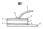
- FIG. 1 is a diagram showing a configuration according to the first embodiment of the present invention.
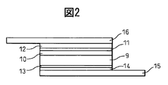
- FIG. 2 is a diagram showing a configuration according to the second embodiment of the present invention.
- the inventor of the present invention uses the electrodes of the semiconductor element and the connection terminals so that the joints of the connection terminals are stable and reliable even when exposed to high temperatures.
- the inventors have found that the difference in linear expansion coefficient between the core material to be formed and the semiconductor element substrate is set to a specific value, and have completed the present invention.
- the terms “electrodes stacked on a wide band gap semiconductor element substrate” and “electrodes” are used to refer to electrodes stacked on a wide band gap semiconductor element substrate, which are directly bonded to connection terminals. Or the electrode which contacts may be said.
- the linear expansion coefficient of the material constituting the semiconductor element is constant within a predetermined temperature range, and the linear expansion of the material constituting the semiconductor element is proportional to the temperature.
- the difference between the linear expansion coefficients is calculated based on the conventionally used silicon (linear expansion coefficient: 2.4 ⁇ 10 -6 / K) and aluminum (linear expansion coefficient: 23 ⁇ 10 -6 / K) linear expansion coefficient (20.6 ⁇ 10 -6 / K) difference in linear expansion coefficient that is 1/4 of the difference (5.2 ⁇ 10 -6 / K), the upper limit temperature can be increased up to four times the conventional upper limit temperature. That is, the difference in coefficient of linear expansion is 5.2 ⁇ 10 which is 1/4 of the difference between the coefficient of linear expansion of silicon and that of aluminum.
- the shearing force can be kept at the same level as the conventional shearing force even in a 600 ° C temperature environment that is about four times the upper limit temperature of 150 ° C at the junction between the silicon substrate and the aluminum wire. It becomes possible.
- the difference in linear expansion coefficient between the core material forming the connection terminal, the semiconductor element substrate, and the electrode member directly bonded to the connection terminal is 5.2 ⁇ 10 -6
- crack fracture at the joint between the core material forming the connection terminal and the electrode which is a portion where thermal stress due to heat cycle is likely to occur, can be suppressed.
- the temperature of 600 ° C. corresponds to the operable temperature of the wide band gap semiconductor.
- the maximum value of the difference in coefficient of linear expansion between the electrode of the semiconductor element, the core material forming the connection terminal, and the semiconductor element substrate is 5.2 ⁇ 10. -6
- / K there is an effect that crack destruction due to a heat cycle to which the power semiconductor element is exposed can be reduced while stably maintaining the conductive connection of the connection portion of the connection terminal.
- This effect is exhibited even in a temperature environment of 150 ° C. or higher where the solder is softened or melted. Further, this effect is exhibited even in an environment having a temperature higher than the melting point of the high-temperature solder, for example, 200 ° C. or higher and 400 ° C. or higher.
- this effect is exhibited even in a temperature environment of 600 ° C. at which a wide band gap semiconductor can operate. That is, in the temperature range of 150 ° C. or more and 600 ° C. or less, there is an effect that it is possible to reduce crack fracture due to heat cycle to which the power semiconductor element is exposed while stably maintaining the conductive connection of the connection portion of the connection terminal. . Further, it is preferable that the difference in coefficient of linear expansion between the electrode of the semiconductor element, the core material forming the connection terminal, and the semiconductor element substrate is as small as possible. Most preferably, the difference in linear expansion coefficient between the electrode of the semiconductor element, the core material forming the connection terminal, and the semiconductor element substrate is zero.
- the difference in coefficient of linear expansion from the semiconductor element substrate is 5.2 ⁇ 10 -6
- the difference in linear expansion coefficient between the electrode of the semiconductor element, the core material forming the connection terminal, and the semiconductor element substrate is preferably 1.5 ⁇ 10. -6 / K or less.
- the difference in coefficient of linear expansion between the core material forming the connection terminal and the electrode is 1.5 ⁇ 10 -6 / K is preferable. Between the core material which forms a connection terminal, and an electrode, it is a location where the load by a heat cycle is easy to be applied. In addition, when used in this specification, a linear expansion coefficient is the value measured on condition of 1 atm and 20 degreeC. In the power semiconductor element of the present invention, the connection between the connection terminal (wire) and the electrode of the semiconductor element is directly joined without using a joining material such as solder and brazing material.
- Such a bonding method includes an ultrasonic wire bonding method in which ultrasonic vibration is applied to the bonding portion and a ball bonding method in which a molten ball is formed by arc discharge or the like at the end of the wire and bonded.
- a joining material such as solder and brazing material
- the bonding method using ultrasonic vibration can be bonded in a short time at normal temperature. For this reason, the mechanical pressure given to an element can also be suppressed and it can join safely, ie, without causing joining failure.
- the material of the semiconductor element substrate used for the power semiconductor element of the present invention is a wide band gap semiconductor material having a band gap of 2.8 eV or more.
- the material of the semiconductor element substrate is silicon carbide (SiC), gallium nitride (GaN), diamond, aluminum gallium nitride (AlGaN), or the like.
- the material of the semiconductor element substrate is particularly preferably silicon carbide (SiC), gallium nitride (GaN), and diamond. These materials have a high intrinsic region temperature which functions as a semiconductor, and can operate as a semiconductor even in a high temperature environment of about 600 ° C.
- the core material forming the connection terminal and the electrode member directly bonded to the connection terminal have a difference in linear expansion coefficient between the three members including the semiconductor element substrate described above. 5.2 ⁇ 10 -6 / K or less is sufficient.
- the core material and the electrode member forming the connection terminal are made of molybdenum (coefficient of linear thermal expansion: 4.9 ⁇ 10 -6 / K), tungsten (thermal expansion coefficient: 4.3 ⁇ 10 -6 / K), chromium (thermal expansion coefficient: 6.2 ⁇ 10 -6 / K), or an alloy thereof.
- alloy means a solid solution or intermetallic compound of a metal containing two or more metal elements.
- metal alloy means a solid solution or intermetallic compound of a metal mainly.
- the term “mainly composed of metal” means containing 50 mol% or more of the metal.
- the core material and the electrode member that form the connection terminal are preferably molybdenum, tungsten, or an alloy thereof.
- molybdenum, tungsten, or an alloy thereof When these metals or alloys are used as connecting wire members, fine wire production by wire drawing is possible.
- an electrode can be formed by sputtering or the like. For this reason, by using molybdenum, tungsten, or an alloy thereof, the core material and each electrode can be easily manufactured, and a flexible element arrangement is possible.
- the electrode may have an interface layer at the interface with the connection terminal and the interface with the semiconductor element substrate as long as the effects of the present invention are not impaired.
- the interface layer is, for example, a thin film formed by sputtering.
- the thickness of the interface layer is preferably 1/5 or less of the thickness of the electrode.
- a connection terminal contains the member which has a predetermined joining surface with respect to electrodes, such as what is called a bus bar, with wire materials, such as what is called a bonding wire.
- regulated by this invention means the linear expansion coefficient of the electrode directly joined with a connection terminal.
- connection terminal in which molybdenum, tungsten, and an alloy thereof are used as a core material and a metal film having a lower resistance than that of the core material is provided.
- a metal film can be formed by, for example, a vapor deposition method or a plating method.
- the metal film is easily formed by a plating method.
- the metal coating material includes gold, silver, copper, aluminum, palladium, and the like. More preferably, the material of the metal coating is selected from gold, silver, or copper. This is because these metals have low electrical resistivity.
- the thickness of the coating is equivalent to the frequency of the high-frequency circuit in which the power semiconductor element is used and the skin depth at the environmental temperature.
- the skin depth L is calculated by the following formula 1.
- f is the frequency (Hz)
- ⁇ is the magnetic permeability (H / m)
- ⁇ is the conductivity (S / m)
- the electrical resistivity of copper near room temperature is 1.7 ⁇ 10 -8 It is about ⁇ m, and the magnetic permeability is about 4 ⁇ ⁇ 10. -7 H / m.
- the relative permeability of copper is approximately 1
- the skin depth when the frequency is 100 kHz is calculated as 0.2 mm from Equation 1. From this, it is understood that when the frequency of the circuit is 100 kHz, a connection terminal having a copper coating having a thickness of about 0.2 mm is preferable.
- the frequency band near 100 kHz is a frequency band generally used in high-frequency circuits, and there are many corresponding electric circuit components.
- the frequency is 100 kHz and the electrical resistivity is 4.0 ⁇ 10 -8
- the skin depth is about 0.3 mm according to Equation 1.
- a round wire having a diameter of 1.2 mm ⁇ or less or a bus bar having a thickness of 1.2 mm or less is generally employed as a dimension of the connection terminal for wiring in the power semiconductor element.
- the thickness of the connection terminal is 1.2 mm
- the electrical resistivity of the metal coating is 4.0 ⁇ 10 -8 When it exceeds ⁇ m, the coating film may be thicker than the core material.
- the influence on the linear expansion coefficient of the joint may be dominant due to the coating component.
- the metal for coating with low electrical resistivity includes silver or gold.
- the electrical resistivity of silver is 1.5 ⁇ 10 -8 ⁇ m
- the electrical resistivity of gold is 2.2 ⁇ 10 -8 ⁇ m.
- the area of the metal film in the cross section of the connection terminal is preferably 70% or less of the area of the cross section of the connection terminal.
- the area of the metal coating in the cross section of the connection terminal is 40% or less of the area of the cross section of the connection terminal.
- connection terminal may employ a core material made of molybdenum, tungsten, chromium, or an alloy thereof alone without forming a metal film.
- the method for forming the metal coating on the surface of the core material may be any method as long as a desired thickness can be formed.
- the method for forming the metal film on the surface of the core material is preferably a hot dip coating method.
- the coating is peeled off from the core material by polishing or the like.
- the electrode is made of molybdenum, tungsten, or an alloy thereof
- the film is peeled off and then ultrasonic bonding is performed between the core material and the electrode. It is preferable to carry out.
- the coating removal step may be omitted.
- FIG. 1 is a diagram showing the configuration of the first embodiment of the present invention.
- a silicon carbide substrate denoted by reference numeral 1 in FIG. 1 (linear expansion coefficient: 4.2 ⁇ 10 -6 / K) is 4H, n-type.
- Silicon carbide substrate 1 is a 5 mm ⁇ 5 mm square material having a thickness of about 200 ⁇ m.
- the homoepitaxial layer of silicon carbide indicated by reference numeral 2 in FIG. 1 has a thickness of about 10 ⁇ m.
- a 1 ⁇ m-thick molybdenum film (linear expansion coefficient: 4.9 ⁇ 10 6) is formed by sputtering.
- Reference numeral 4 in FIG. 1 denotes a nickel film having a thickness of 0.3 ⁇ m formed by sputtering. After the nickel film 4 is formed, heat treatment is performed at 1000 ° C. for about 2 minutes, and an ohmic is formed on the back surface of the silicon carbide substrate (semiconductor element substrate) 1. Further, molybdenum metal (film) 5 is formed on the surface of the nickel film 4 by sputtering to a thickness of about 2 ⁇ m.
- the bus bar (connection terminal) 6 is a flat molybdenum core material having a width of 5 mm and a thickness of 0.6 mm (linear expansion coefficient: 4.9 ⁇ 10 -6 / K), and the surface and the back surface of the molybdenum core material are each plated with a copper thickness of 0.2 mm.
- the bus bar 6 is bonded to the molybdenum film 5 by ultrasonic bonding.
- the copper plating thickness is 1.7 ⁇ 10 times the electrical resistivity of copper. -8 ⁇ m, permeability is about 4 ⁇ ⁇ 10 -7 It is calculated by the above-mentioned formula 1 where H / m and the operating frequency are 100 kHz.
- a protective tape is applied to the molybdenum film 3 formed on one surface of the silicon carbide substrate 1. Silicon carbide substrate 1 is placed on the pedestal so that molybdenum film 3 to which the protective tape is attached faces the pedestal of the ultrasonic bonding apparatus.
- a bus bar is mounted on the surface of the molybdenum film 5, and an ultrasonic vibration terminal having a diameter of 3 mm ⁇ is uniformly pressed against the surface of the contact portion of the bus bar to be joined.
- the frequency of the ultrasonic wave used is 100 kHz, and the amplitude is 1 ⁇ m.
- the bus bar bonding portion connected to the element electrode has the copper coating of the bus bar peeled off by the abrasive paper and the bonding surface is made smooth before ultrasonic bonding.
- the wire (connection terminal) 7 is bonded to the molybdenum film 3.
- the wire 7 has molybdenum having a diameter of 0.6 mm as a core material.
- copper is coated with a thickness of 0.2 mm.
- the frequency of the ultrasonic wave is 100 kHz, and the amplitude is 1 ⁇ m. Similar to the bus bar bonding, the ultrasonic bonding portion of the wire 7 is connected in a state where the coating is peeled off by polishing and the bonding surface is smooth.
- a current of 120 A was applied in the forward direction of the Schottky diode element formed by the above method. In a steady state in which a current of 120 A was applied, the surface temperature of the element observed by the radiation thermometer was 200 ° C. When the polarity of the applied voltage was reversed from this state, the energization current was cut off. When returning to the forward direction again, the same energization as before was confirmed.
- the diode functions normally even when the temperature of the element reaches 150 ° C. or higher. Furthermore, after repeating DC energization and interruption for 1,000 hours and 12,000 times at intervals of 5 minutes, the bonding sites formed on the front surface and the back surface of the element were observed with a microscope. No cracks or the like were found at the bonding sites formed on the front and back surfaces of the device. Further, in order to investigate the high frequency characteristics of the Schottky diode element formed by the above-described method, the element was energized under the condition that the ON / OFF cycle of the diode was 100 kHz and the energization current was 120 A. The temperature of the device surface under these conditions was about 250 ° C.
- This temperature is about 50 ° C. higher than that during direct current application.
- another element within the scope of the present invention was formed.
- the size of the molybdenum wire and bus bar to which this element is connected is the same as the size of the molybdenum wire and bus bar described above. However, both the molybdenum wire to which this element is connected and the bus bar do not have copper plating.
- This element was energized under ON / OFF conditions of 100 kHz / 120A.
- the steady state temperature was 280 ° C. This temperature is about 80 ° C. higher than that during direct current application.
- the temperature rise in the previous embodiment using the wire material plated with copper and the element to which the bus bar is connected is about 30 ° C.
- the surface temperature of the steady-state element observed by the radiation thermometer was 250 ° C.
- the energization current was cut off.
- the same energization as before was confirmed. From these, it is understood that the diode functions normally even when the temperature of the element reaches 150 ° C. or higher.
- an experiment was conducted in which DC energization and interruption were repeated 12,000 times for 1000 hours at intervals of 5 minutes. However, after about 1 hour, the device was not energized. Then, the cause was investigated by microscopic observation.
- FIG. 2 is a diagram showing the configuration of the second exemplary embodiment of the present invention.
- An n-type GaN substrate denoted by reference numeral 9 in FIG. 2 (coefficient of thermal expansion: 5.6 ⁇ 10 6 -6 / K) is a square material with a thickness of about 300 ⁇ m and a size of 3 mm ⁇ 3 mm.
- the thickness of the homoepitaxial layer (film) of GaN indicated by reference numeral 10 in the figure is about 10 ⁇ m.
- a palladium film (linear expansion coefficient: 11.8 ⁇ 10 6) having a thickness of 0.2 ⁇ m is formed on the epitaxial film by sputtering.
- -6 / K) 11 is formed, and a Schottky electrode is formed.
- a tungsten electrode having a thickness of 2 ⁇ m (linear expansion coefficient: 4.3 ⁇ 10 -6 / K) 12 is formed by sputtering.
- symbol 13 of FIG. 2 is the multilayer film of titanium and gold formed by the sputtering method, and thickness is 0.3 micrometer. After the multilayer film 13 is formed, a heat treatment is performed at 900 ° C.
- the bus bar 15 has a flat tungsten core material having a width of 3 mm and a thickness of 0.6 mm, and the front surface and the back surface of the core material are subjected to gold plating with a thickness of 0.25 mm.
- the bus bar 15 is bonded to the tungsten film 14 by ultrasonic bonding.
- the thickness of the gold plating is 2.4 x 10 times the electrical resistivity of gold.
- permeability is about 4 ⁇ ⁇ 10 -7 It is calculated from the above equation 1 where H / m and the operating frequency is 100 kHz.
- a protective tape is applied to the tungsten film 12 formed on one surface of the GaN substrate.
- the GaN substrate 9 is placed on the pedestal so that the tungsten film 14 to which the protective tape is attached faces the pedestal of the ultrasonic bonding apparatus.
- a bus bar is mounted on the surface of the tungsten film 14, and an ultrasonic vibration terminal having a diameter of 3 mm ⁇ is uniformly pressed against the surface of the contact portion of the bus bar to be joined.
- the frequency of the ultrasonic wave used is 100 kHz, and the amplitude is 1 ⁇ m.
- the joint of the bus bar connected to the tungsten film 14 is made to have a smooth joining surface by peeling the gold film with abrasive paper before ultrasonic joining.
- the wire (connection terminal) 16 is bonded to the tungsten film 12.
- the wire 16 is made of molybdenum having a diameter of 0.6 mm as a core, and gold is coated on the surface of the core with a thickness of 0.25 mm.
- ultrasonic bonding is performed on the tungsten film 12 and the wire 16.
- the frequency of the ultrasonic wave is 100 kHz, and the amplitude is 1 ⁇ m.
- the ultrasonic bonding portion of the bus bar 16 is connected with the coating surface peeled off by polishing and the bonding surface being smooth.
- a current of 150 A was applied in the forward direction of the Schottky diode element formed by the above method.
- the surface temperature of the element observed by the radiation thermometer was 250 ° C.
- the energization current was cut off.
- the same energization as before was confirmed. From these, it is understood that the diode functions normally even when the temperature of the element reaches 150 ° C. or higher.
- the bonding sites formed on the front surface and the back surface of the element were observed with a microscope. No cracks or the like were found at the bonding sites formed on the front and back surfaces of the device.
- the element was energized under the condition that the ON / OFF cycle of the diode was 100 kHz and the energization current was 150 A.
- the temperature of the element surface under these conditions was about 300 ° C. This temperature is about 50 ° C. higher than that during direct current application.
- another element within the scope of the present invention was formed.
- both bus bars to which this element is connected are the same as the bus bar described above. However, both bus bars to which this element is connected do not have gold plating.
- This element was energized under ON / OFF conditions of 100 kHz / 150A.
- the steady state temperature was 340 ° C. This temperature is about 90 ° C. higher than that during direct current application.
- the temperature rise in the previous embodiment using the element to which both the gold-plated bus bars are connected is about 40 ° C. lower than the temperature rise in this embodiment. From this, the reduction effect of AC loss by copper plating, that is, the effect of suppressing the apparent increase in electrical resistance was confirmed.
- a Schottky diode element similar to that of the second example was manufactured except that bus bars 15 and 16 made of copper were used.
- the configuration and assembly method of this Schottky diode element are the same as in the second embodiment.
- the electrical resistivity of the copper bus bar (1.7 ⁇ 10 10 -8 (Approx. ⁇ m) is sufficiently low so that no film is applied.
- 150A was energized in the forward direction of the Schottky diode element of this comparative example.
- the surface temperature of the steady-state element observed by the radiation thermometer was 200 ° C. When the polarity of the applied voltage was reversed from this state, the energization current was cut off.
- a silicon carbide substrate and a GaN substrate are used as the semiconductor element substrate.
- the present invention is also applicable to an element using diamond or AlGaN as a semiconductor element substrate.
- molybdenum and tungsten are used as the connection terminal and the electrode.
- chromium or an alloy system mainly composed of chromium is used as the connection terminal and the electrode, the difference in coefficient of linear expansion between the connection terminal, the electrode, and the semiconductor element substrate is 5.2 ⁇ . 10 -6 / K can be used.
- the present invention can be applied regardless of the structure of the element such as MOSFET, JFET, MESFET, PiN diode, IGBT, thyristor, etc. as well as a Schottky diode.
Landscapes
- Electrodes Of Semiconductors (AREA)
- Wire Bonding (AREA)
Abstract
150℃以上のような、ワイドバンドギャップ半導体が作動可能な温度環境下であっても、電極、接続 端子、及び半導体素子基板が導通接続されながら、ヒートサイクルによる亀裂破壊が低減された接合部 を有する電力用半導体素子を提供する。 ワイドバンドギャップ半導体素子基板に電極が積層されると共に、電極には外部配線へ接続するための接続端子が接合されており、150℃以上の温度環境下で作動可能な電力用半導体素子であって、前記電極、接続端子を形成する芯材、及び前記半導体素子基板の3つの線膨脹係数の差が、最大で5.2 ×10⁻⁶/Kであり、かつ、前記接続端子と電極とが直接接合されてなる接合部を有することを特徴とする電力用半導体素子である。
Description
本発明は、高温環境下で使用可能な電力用半導体素子に関する。
電力変換用の素子として、ダイオード、トランジスタ、MOSFET、及びIGBTなどが採用される。これら素子は、一般にシリコン半導体材料により形成される。素子製造プロセスにより種々の処理が施されたシリコン半導体材料をダイシングすることによって、所定の機能を有する半導体チップが取得される。半導体チップは、半導体チップ表面に形成される電極が、他端が外部と接続するための電極に接続されるワイヤー(接続線)に半田を介して接合され、素子やモジュールとして組み立てられる。
半導体チップ表面に形成される電極と、ワイヤーとの接合に使用される半田は、一般的にSn/Pb系である。Sn/Pb系半田の融点は、約180℃である。半田の融点付近まで半田の温度が上昇すると、半田が軟化して、半導体チップ表面に形成される電極と、ワイヤーとの間の接合を維持できなくなる可能性がある。このため、表面に形成される電極と、ワイヤーとの間の接合にSn/Pb系半田が使用される半導体素子は、150℃程度の温度以下の温度で使用されることが一般的である。また、半田が使用される半導体素子において、ヒートサイクル破壊モードも知られている。ヒートサイクル破壊モードは、半田の溶融温度に到達しない場合であっても、通電、非通電の繰り返し等で生じる破壊モードである。ヒートサイクル破壊モードは、半導体チップ、ワイヤー、及び半田の個々の線膨脹係数が異なるため、これらの接合部にせん断応力が生じ、ヒートサイクルにより亀裂が発生し、接合部が破壊されるという現象である(非特許文献1参照)。
半田によって接合される接合部の信頼性を高めるための種々の技術が知られる。特許文献1には、接続端子と半導体素子とを接合するために、融点が異なる2種類の半田を用いる技術が開示されている。半田厚みを確保するために高融点の半田を使用するとともに、高融点の半田は、低融点の半田で被膜される。
また、特許文献2には、シリコン半導体チップとアルミニウムワイヤーとが使用されるパワー半導体モジュールにおける問題点が開示される。シリコンチップと、アルミニウムワイヤーとは、線膨脹率に大きな差ある。このため、モジュールが加熱、又は冷却するときにワイヤーとパッド(電極)との間の接合界面に高い熱応力が発生する。この熱応力が繰り返して働くことにより、短時間でワイヤーが剥離する可能性がある。そして、このような問題を解決するために、超音波ワイヤーボンディングでパッドに接合されたアルミニウムワイヤー接合部に発生する熱応力、具体的にはパッドに接合されたワイヤーに発生する引張応力を軽減するように、パッドに溝を形成するなどの幾何学的な加工を施す技術が開示されている。
半導体チップと接続されるワイヤーとして、一般的に、金(Au)、銅(Cu)、及びアルミニウム(Al)等を主とした金属ワイヤーが使用される。特許文献3には、半導体装置、又は電子機器類の内部で使用される電子ワイヤー用複合金属線材が開示される。この電子ワイヤー用複合金属線材は、タングステン(W)の芯を銅(Cu)被覆層で被覆することにより、極細線での強度を確保することを可能にする。
一方、近年、従来のシリコン半導体材料と比較して、半導体として機能とする真性領域温度が高く、高温での動作が可能であり、かつ飽和ドリフト速度、及び絶縁破壊電界が大きいワイドバンドギャップ半導体と称される炭化珪素(SiC)、窒化ガリウム(GaN)、及びダイヤモンド等の素子を用いたデバイスの開発や実用化が進みつつある。ワイドバンドギャップ半導体では、250℃~600℃の高温下での動作実験も報告されている(非特許文献2)。
ワイドバンドギャップ半導体により形成される素子を使用することにより、高温下で素子を動作させることが可能になる。例えば、野外、又は自動車の車内などの高温下に曝される環境下において、ワイドバンドギャップ半導体により形成される素子は、空冷などの簡便な冷却装置によって安定的に動作させることが可能である。また、ワイドバンドギャップ半導体は、電流密度が高く、又は高周波動作で動作するために素子の温度が高くなる場合でも、最大使用温度に自由度を持たせることができるなど、従来のシリコン半導体にはない利点を持つ。さらに、絶縁破壊電界強度が高いため、ショットーキバリヤダイオード、及びMOSFETなどのユニポーラデバイスを、高電圧の高周波スイッチング回路において使用できるため、高出力電源機器を小型化できるなどの利点を有する。
半導体チップ表面に形成される電極と、ワイヤーとの接合に使用される半田は、一般的にSn/Pb系である。Sn/Pb系半田の融点は、約180℃である。半田の融点付近まで半田の温度が上昇すると、半田が軟化して、半導体チップ表面に形成される電極と、ワイヤーとの間の接合を維持できなくなる可能性がある。このため、表面に形成される電極と、ワイヤーとの間の接合にSn/Pb系半田が使用される半導体素子は、150℃程度の温度以下の温度で使用されることが一般的である。また、半田が使用される半導体素子において、ヒートサイクル破壊モードも知られている。ヒートサイクル破壊モードは、半田の溶融温度に到達しない場合であっても、通電、非通電の繰り返し等で生じる破壊モードである。ヒートサイクル破壊モードは、半導体チップ、ワイヤー、及び半田の個々の線膨脹係数が異なるため、これらの接合部にせん断応力が生じ、ヒートサイクルにより亀裂が発生し、接合部が破壊されるという現象である(非特許文献1参照)。
半田によって接合される接合部の信頼性を高めるための種々の技術が知られる。特許文献1には、接続端子と半導体素子とを接合するために、融点が異なる2種類の半田を用いる技術が開示されている。半田厚みを確保するために高融点の半田を使用するとともに、高融点の半田は、低融点の半田で被膜される。
また、特許文献2には、シリコン半導体チップとアルミニウムワイヤーとが使用されるパワー半導体モジュールにおける問題点が開示される。シリコンチップと、アルミニウムワイヤーとは、線膨脹率に大きな差ある。このため、モジュールが加熱、又は冷却するときにワイヤーとパッド(電極)との間の接合界面に高い熱応力が発生する。この熱応力が繰り返して働くことにより、短時間でワイヤーが剥離する可能性がある。そして、このような問題を解決するために、超音波ワイヤーボンディングでパッドに接合されたアルミニウムワイヤー接合部に発生する熱応力、具体的にはパッドに接合されたワイヤーに発生する引張応力を軽減するように、パッドに溝を形成するなどの幾何学的な加工を施す技術が開示されている。
半導体チップと接続されるワイヤーとして、一般的に、金(Au)、銅(Cu)、及びアルミニウム(Al)等を主とした金属ワイヤーが使用される。特許文献3には、半導体装置、又は電子機器類の内部で使用される電子ワイヤー用複合金属線材が開示される。この電子ワイヤー用複合金属線材は、タングステン(W)の芯を銅(Cu)被覆層で被覆することにより、極細線での強度を確保することを可能にする。
一方、近年、従来のシリコン半導体材料と比較して、半導体として機能とする真性領域温度が高く、高温での動作が可能であり、かつ飽和ドリフト速度、及び絶縁破壊電界が大きいワイドバンドギャップ半導体と称される炭化珪素(SiC)、窒化ガリウム(GaN)、及びダイヤモンド等の素子を用いたデバイスの開発や実用化が進みつつある。ワイドバンドギャップ半導体では、250℃~600℃の高温下での動作実験も報告されている(非特許文献2)。
ワイドバンドギャップ半導体により形成される素子を使用することにより、高温下で素子を動作させることが可能になる。例えば、野外、又は自動車の車内などの高温下に曝される環境下において、ワイドバンドギャップ半導体により形成される素子は、空冷などの簡便な冷却装置によって安定的に動作させることが可能である。また、ワイドバンドギャップ半導体は、電流密度が高く、又は高周波動作で動作するために素子の温度が高くなる場合でも、最大使用温度に自由度を持たせることができるなど、従来のシリコン半導体にはない利点を持つ。さらに、絶縁破壊電界強度が高いため、ショットーキバリヤダイオード、及びMOSFETなどのユニポーラデバイスを、高電圧の高周波スイッチング回路において使用できるため、高出力電源機器を小型化できるなどの利点を有する。
両角朗、山田克己、宮坂忠志"パワー半導体モジュールにおける信頼性設計技術"富士時報 vol.74 No.2 p.145−148(2001)
吉田貞史"ワイドバンドギャップ半導体による高パワーデバイス特性の向上"電子技術総合研究所彙報 第62巻 第10,11号 p.493−507(1998)
ワイドバンドギャップ半導体材料で形成される素子が高温で動作されるとき、ワイドバンドギャップ半導体材料と、接続端子とを接合する接合部材として半田を採用することはできない。上述のように一般的に使用される半田の融点は、180℃程度であり、この温度は、ワイドバンドギャップ半導体材料で形成される素子の動作可能な温度よりも低いためである。例えば、Sn/Pb系半田では、150℃以上の温度で半田が軟化して、電気的な接合を維持できない。また、高い融点を有する他の成分系の半田を採用する場合であっても、半田として適切な特性を有する材料系は、260℃以下である。このため、260℃以上の温度で電気的な接合を維持することができる半田は、存在しない。
一方、半田接合以外の接合技術として、アルミニウムワイヤー等を半導体チップに直接圧着を行う技術がある。しかしながら、アルミニウムワイヤー等の材料と、半導体チップとは、線膨脹係数に差があるために、ヒートサイクルによって、圧着接合部が破壊される可能性がある。両者の線膨脹係数は、室温付近では1桁異なる。具体的には、ワイドバンドギャップ半導体である炭化珪素の線膨脹係数は、4.2×10⁻⁶/K(a軸)であり、GaNの線膨脹係数は、5.6×10−6/K(a軸)であり、ダイヤモンドの線膨脹係数は、1.1×10−6/Kである。一方、パワーデバイスの接合ワイヤーとして一般的に使用されるアルミニウムの線膨脹係数は、23×10−6/K、銅の線膨脹係数は、16.8×10−6/K、金の線膨脹係数は、14.3×10−6/Kである。現在主流であるシリコン半導体材料の線膨脹係数は2.4×10−6/Kである。例えば特許文献2のように、アルミニウムワイヤーの圧着接合部を形成するパッドの幾何学的構造を適当な構造にすることにより、従来のシリコン半導体材料が使用可能な温度範囲では、シリコン半導体材料とワイヤーとの間の線膨脹係数の差に起因する問題は回避可能であった。しかしながらワイドバンドギャップ半導体材料で形成される素子を高温で動作させる場合、上述のようにパッドの幾何学的構造を適当な構造にすることのみでは、シリコン半導体材料とワイヤーとの間の線膨脹係数の差に起因する問題は回避することができない。
特許文献3には、タングステンを芯材として銅を被覆層とした電子ワイヤー用複合金属線が開示される。しかしながら、特許文献3には、半導体材料を接合した具体的な例は、全く記載されていない。特許文献3に記載されるワイヤーは、極細線化が必要な用途で使用される。可撓性を備え、かつ低い導体抵抗を実現するために、特許文献3に記載されるワイヤーの線径は、15μm以下である。このため、特許文献3に記載されるワイヤーは、ワイドバンドギャップ半導体を用いた素子には使用できない。特に、電力用半導体素子に使用する場合には、ワイヤーに大電が流れるために、特許文献3に記載されるワイヤーを使用することは、現実的ではない。また、150℃以上高温下で電力用半導体素子として使用される場合は、半導体素子基板と接続線との線膨脹係数の差によって、これらの接合部が亀裂破壊する可能性がある。
本発明は、上述の問題を鑑み、従来の半田が軟化、及び溶融する150℃以上のワイドバンドギャップ半導体が作動可能な温度環境下において、半導体素子の電極と、接続線と、半導体素子基板とがそれぞれ導通接続され、ヒートサイクルによる亀裂破壊が生じる可能性が低減される接合部を有する電力用半導体素子を提供することを目的とする。さらに信頼性の高い接合部を有するとともに、高周波数で素子が動作する場合でも、電力損失の小さい電力用半導体素子を提供することを目的とする。
一方、半田接合以外の接合技術として、アルミニウムワイヤー等を半導体チップに直接圧着を行う技術がある。しかしながら、アルミニウムワイヤー等の材料と、半導体チップとは、線膨脹係数に差があるために、ヒートサイクルによって、圧着接合部が破壊される可能性がある。両者の線膨脹係数は、室温付近では1桁異なる。具体的には、ワイドバンドギャップ半導体である炭化珪素の線膨脹係数は、4.2×10⁻⁶/K(a軸)であり、GaNの線膨脹係数は、5.6×10−6/K(a軸)であり、ダイヤモンドの線膨脹係数は、1.1×10−6/Kである。一方、パワーデバイスの接合ワイヤーとして一般的に使用されるアルミニウムの線膨脹係数は、23×10−6/K、銅の線膨脹係数は、16.8×10−6/K、金の線膨脹係数は、14.3×10−6/Kである。現在主流であるシリコン半導体材料の線膨脹係数は2.4×10−6/Kである。例えば特許文献2のように、アルミニウムワイヤーの圧着接合部を形成するパッドの幾何学的構造を適当な構造にすることにより、従来のシリコン半導体材料が使用可能な温度範囲では、シリコン半導体材料とワイヤーとの間の線膨脹係数の差に起因する問題は回避可能であった。しかしながらワイドバンドギャップ半導体材料で形成される素子を高温で動作させる場合、上述のようにパッドの幾何学的構造を適当な構造にすることのみでは、シリコン半導体材料とワイヤーとの間の線膨脹係数の差に起因する問題は回避することができない。
特許文献3には、タングステンを芯材として銅を被覆層とした電子ワイヤー用複合金属線が開示される。しかしながら、特許文献3には、半導体材料を接合した具体的な例は、全く記載されていない。特許文献3に記載されるワイヤーは、極細線化が必要な用途で使用される。可撓性を備え、かつ低い導体抵抗を実現するために、特許文献3に記載されるワイヤーの線径は、15μm以下である。このため、特許文献3に記載されるワイヤーは、ワイドバンドギャップ半導体を用いた素子には使用できない。特に、電力用半導体素子に使用する場合には、ワイヤーに大電が流れるために、特許文献3に記載されるワイヤーを使用することは、現実的ではない。また、150℃以上高温下で電力用半導体素子として使用される場合は、半導体素子基板と接続線との線膨脹係数の差によって、これらの接合部が亀裂破壊する可能性がある。
本発明は、上述の問題を鑑み、従来の半田が軟化、及び溶融する150℃以上のワイドバンドギャップ半導体が作動可能な温度環境下において、半導体素子の電極と、接続線と、半導体素子基板とがそれぞれ導通接続され、ヒートサイクルによる亀裂破壊が生じる可能性が低減される接合部を有する電力用半導体素子を提供することを目的とする。さらに信頼性の高い接合部を有するとともに、高周波数で素子が動作する場合でも、電力損失の小さい電力用半導体素子を提供することを目的とする。
150℃以上の温度環境下で作動可能な電力用半導体素子であって、ワイドバンドギャップ半導体素子基板と、ワイドバンドギャップ半導体素子基板に積層される電極と、電極に接合される外部配線へ接続するための接続端子と、を有し、電極、接続端子を形成する芯材、及び半導体素子基板の3つの線膨脹係数の差が、最大で5.2×10⁻⁶/Kであり、接続端子と電極とを接合する接合部は、接続端子と電極とが直接接合されること特徴とする電力用半導体素子である。
半導体素子を形成する電極と接続端子とは、超音波振動により接合されていることが好ましい。また、半導体素子基板は、炭化珪素、GaN、又はダイヤモンドであることが好ましい。更に、電極は、モリブデン、タングステン、または、これらの1種以上を含有する化合物(又は合金)で構成されることが好ましい。更にまた、接続端子を形成する芯材が、モリブデン、タングステン、または、これらの1種以上を含有する化合物(又は合金)であることが好ましい。
また、接続端子については、電気抵抗率が4×10⁻⁸Ωm以下の金属被膜で芯材を被覆するようにしても良いが、その場合、金属被膜を有した接続端子の横断面における金属の被膜面積が、横断面に対して70%以下となるようにするのが好ましい。
半導体素子を形成する電極と接続端子とは、超音波振動により接合されていることが好ましい。また、半導体素子基板は、炭化珪素、GaN、又はダイヤモンドであることが好ましい。更に、電極は、モリブデン、タングステン、または、これらの1種以上を含有する化合物(又は合金)で構成されることが好ましい。更にまた、接続端子を形成する芯材が、モリブデン、タングステン、または、これらの1種以上を含有する化合物(又は合金)であることが好ましい。
また、接続端子については、電気抵抗率が4×10⁻⁸Ωm以下の金属被膜で芯材を被覆するようにしても良いが、その場合、金属被膜を有した接続端子の横断面における金属の被膜面積が、横断面に対して70%以下となるようにするのが好ましい。
本発明によれば、150℃以上のような、ワイドバンドギャップ半導体が作動可能な温度環境下において、半導体素子の電極、接続端子、及び半導体素子基板が導通接続され、ヒートサイクルによる亀裂破壊が生じる可能性が低減される接合部を有する電力用半導体素子を提供することができる。よって、高温動作可能な信頼性の高い電力用半導体素子を提供できる。さらに信頼性の高い接合部を有するとともに、高周波数で素子が動作する場合でも、電力損失の小さい電力用半導体素子を提供することができる。
図1は、本発明の第1の実施形態に係わる構成を示す図である。
図2は、本発明の第2の実施形態に係わる構成を示す図である。
図2は、本発明の第2の実施形態に係わる構成を示す図である。
以下に詳細に説明されるように、本発明の発明者は、接続端子の接合部が高温にさらされても安定で、かつ信頼性の高くなるように、半導体素子の電極と、接続端子を形成する芯材と、半導体素子基板との間の線膨脹率の差を特定の値にすることを見出し、本発明を完成するに至った。
本明細書において、用語「ワイドバンドギャップ半導体素子基板に積層される電極」、及び「電極」を使用して、ワイドバンドギャップ半導体素子基板に積層される電極であって、接続端子に直接接合、又は接触する電極をいう場合がある。
半導体素子を構成する材料の線膨脹係数は、所定の温度範囲内で一定であり、かつ半導体素子を構成する材料の線膨張は、温度に比例すると仮定する。このような仮定に基づくと、線膨脹係数の差を、従来から使用されるシリコン(線膨張係数:2.4×10⁻⁶/K)とアルミニウム(線膨脹係数:23×10−6/K)との間の線膨脹係数(20.6×10−6/K)の差の1/4である線膨脹率の差(5.2×10−6/K)にする場合、従来の上限温度の4倍まで上限温度を上昇させることが可能になる。すなわち、線膨脹係数の差をシリコンの線膨張係数と、アルミニウムの線膨脹係数との差の1/4である5.2×10−6/Kにすることにより、シリコン基板とアルミニウムワイヤーとの間の接合部における上限温度150℃の約4倍となる600℃温度環境下でも、従来のせん断力と同程度のせん断力にとどめることが可能となる。接続端子を形成する芯材と、半導体素子基板と、接続端子に直接接合される電極部材との間の線膨脹係数の差が、5.2×10−6/Kになるような組み合せることにより、ヒートサイクルによる熱応力が生じやすい部分である、接続端子を形成する芯材と電極との間の接合部の亀裂破壊が抑制できる。上述のように600℃の温度は、ワイドバンドギャップ半導体の動作可能な温度に相当する。
したがって、電力用半導体素子において、半導体素子の電極と、接続端子を形成する芯材と、半導体素子基板との間の線膨脹係数の差の最大値を、5.2×10⁻⁶/Kとすることにより、接続端子の接合部の導通接続を安定的に維持しながら、電力用半導体素子が曝されるヒートサイクルによる亀裂破壊を低減できるという効果を奏する。この効果は、半田が軟化し、又は溶解する150℃以上の温度環境下であっても奏される。更に、この効果は、高温半田の融点以上の温度、例えば、200℃以上、及び400℃以上の温度の環境下であっても奏される。上述したように、ワイドバンドギャップ半導体の作動可能な600℃の温度環境下でも、この効果を奏する。即ち、少なくとも150℃以上600℃以下の温度範囲において、接続端子の接合部の導通接続を安定的に維持しながら、電力用半導体素子が曝されるヒートサイクルによる亀裂破壊を低減できるという効果を奏する。
また、半導体素子の電極と、接続端子を形成する芯材と、半導体素子基板との間の線膨脹係数の差は、小さいほど好ましい。最も好ましくは、半導体素子の電極と、接続端子を形成する芯材と、半導体素子基板との間の線膨脹係数の差は、ゼロである。しかしながら、様々な種類の材料を組み合せる場合に、半導体素子の電極と、接続端子を形成する芯材と、半導体素子基板との間の線膨脹係数の差をゼロにことは困難である。このため、接続端子を形成する芯材と、半導体素子基板との間の線膨脹係数の差をゼロにすることが可能な材料の組み合せは、限定される。一方、半導体素子基板との間の線膨脹係数の差を5.2×10⁻⁶/K以内にまで広げると、幅広い種類の材料から材料を選択することが可能になる。半導体素子の電極と、接続端子を形成する芯材と、半導体素子基板との間の線膨脹係数の差は、好ましくは1.5×10−6/K以内である。さらに、接続端子を形成する芯材と、電極との間の線膨脹係数の差が1.5×10−6/K以内となるようにすることが好ましい。接続端子を形成する芯材と、電極との間は、ヒートサイクルによる負荷が掛かり易い箇所である。なお、本明細書において使用される場合、線膨張係数は、1atm、20℃の条件の下で測定した値である。
本発明の電力用半導体素子において、接続端子(ワイヤー)と、半導体素子の電極との間の接続は、半田、及びロウ材などの接合材料を介せずに、直接接合される。このような接合方法は、接合部に超音波振動を与えて接合する超音波ワイヤーボンディング法、及びワイヤー端部をアーク放電等で溶融ボールを形成して接合するボールボンディング法などが含まれる。これらの接合方法では、半田、及びロウ材などの接合材料が使用されないため、150℃以上の高温でも接合材料の軟化、又は溶融に起因する接続不良が生じる虞はない。超音波振動を利用した接合方法は、常温で短時間に接合することができる。このため、素子に与える機械的圧力も抑制することができ、安全に、すなわち接合不良を起こさずに接合できる。このように、超音波振動を利用して接合部を形成することは、信頼性の高い接合部を形成することができるので、好ましい。
本発明の電力用半導体素子に使用される半導体素子基板の材料は、バンドギャップが2.8eV以上のワイドバンドギャップ半導体材料である。例えば、半導体素子基板の材料は、炭化珪素(SiC)、窒化ガリウム(GaN)、ダイヤモンド、及び窒化アルミニウムガリウム(AlGaN)などである。半導体素子基板の材料は、炭化珪素(SiC)、窒化ガリウム(GaN)、及びダイヤモンドであることは、特に好ましい。これらの材料は、半導体として機能とする真性領域温度が高く、600℃程度の高温環境下でも半導体としての動作が可能である。
本発明に係る電力用半導体素子において、接続端子を形成する芯材、及び接続端子に直接接合される電極部材は、上述の半導体素子基板を含めた3つの部材の間の線膨脹係数の差が5.2×10−6/K以下となるものであればよい。例えば、接続端子を形成する芯材、及び電極部材は、モリブデン(線熱膨張係数:4.9×10−6/K)、タングステン(熱膨張係数:4.3×10−6/K)、クロム(熱膨張係数:6.2×10−6/K)、又はそれらの合金である。本明細書で使用されるとき、用語「合金」は、2種以上の金属元素を含む金属の固溶体、金属間化合物を意味する。また用語「金属の合金」は、金属を主要とする金属の固溶体、金属間化合物を意味する。ここで用語「金属を主要とする」は、その金属を50モル%以上含むことを意味する。接続端子を形成する芯材、及び電極部材は、モリブデン、タングステン、又はそれらの合金であることが好ましい。これらの金属、又は合金が接続線部材として使用される場合、伸線による細線製造が可能である。また、これらの金属、又は合金を電極部材として使用する場合、スパッタリング等により電極を形成することが可能である。このため、モリブデン、タングステン、又はそれらの合金を採用することにより、芯材、及び電極それぞれは、容易に製造することが可能であり、かつ柔軟な素子配置が可能である。電極は、接続端子との間の界面、及び半導体素子基板との間の界面に、本発明が奏する作用効果を損なわない範囲で界面層を有していてもよい。界面層は、例えばスパッタによる薄膜などである。界面層の厚さは、電極の厚さの1/5以下の厚さであることが好ましい。なお、本発明において、接続端子は、いわゆるボンディングワイヤー等の線材とともに、いわゆるブスバーなど電極に対して所定の接合面を有して接合される部材を含む。また、本発明で規定される電極の線膨張係数は、接続端子と直接接合される電極の線膨張係数を意味する。
また、本発明における電力用半導体素子が、高周波回路で使用される場合、接続端子に流れる電流は、表皮効果により端子表面に集中して流れる。このため、比較的電気抵抗が高いモリブデン、タングステン、及びそれらの合金からなる接続端子では損失が増大するおそれがある。損失を抑制するために、高周波電流の抵抗成分を減じることが望ましい。そこで、モリブデン、タングステン、及びそれらの合金を芯材とし、芯材よりも低い抵抗を有する金属の被膜を設ける接続端子を採用することが好ましい。このような金属被膜は、例えば、蒸着法やメッキ法で形成することが可能である。金属被膜は、メッキ法で容易に形成される。具体的には、金属被膜の材料は、金、銀、銅、アルミニウム、及びパラジウムなどがある。金属被膜の材料は、金、銀、又は銅から選択することがより好ましい。これらの金属は、電気抵抗率が低いためである。さらに、被膜の厚さは、電力用半導体素子が使用される高周波回路の周波数、及び環境温度における表皮深さと同等程度の厚さであることが望ましい。表皮深さLは下記の式1により算出される。
 ここで、fは周波数(Hz)、μは透磁率(H/m)、σは導電率(S/m)であり、電気抵抗率の逆数である。
例えば、室温付近での銅の電気抵抗率は、1.7×10−8Ωm程度であり、透磁率は、約4π×10−7H/mである。ここで、銅の比透磁率はほぼ1であることを考慮し、μ=μ0=4π×10−7H/mと仮定した。これから、周波数が100kHzのときの表皮深度は、式1から0.2mmと計算される。これから、回路の周波数が100kHzの場合、厚さが0.2mm程度である銅被膜を有する接続端子が好ましいことが理解される。100kHzの近傍の周波数帯域は、高周波回路で一般に使用される周波数帯域であり、対応する電気回路部品も多い。周波数が100kHzであり、電気抵抗率が4.0×10−8Ωmである金属の被膜が使用される場合、式1により表皮深さは、約0.3mmとなる。電力用半導体素子内の配線用の接続端子の寸法は、一般的に、直径が1.2mmφ以下である丸線、又は厚さが1.2mm以下であるブスバーが採用される。接続端子の厚さが1.2mmである場合、被膜の厚さが接続端子の厚さ方向に合計で0.6mm(=0.3mm×2)となり、芯材とほぼ同じ厚さになる。さらに、金属の被膜の電気抵抗率が4.0×10−8Ωmを超える場合には、被膜が芯材の厚さをよりも厚くなる可能性がある。この場合、接合部の線膨脹係数に与える影響は、被膜成分による影響が支配的となる可能性がある。なお、電気抵抗率が低い被膜用の金属は、銀、又は金などがある。銀の電気抵抗率は、1.5×10−8Ωmであり、金の電気抵抗率は、2.2×10−8Ωmである。
また、これまでの説明に基づくと、接続端子の横断面における金属被膜の面積は、接続端子の横断面の面積の70%以下の面積であることが良い。好ましくは、接続端子の横断面における金属被膜の面積は、接続端子の横断面の面積の40%以下である。なお、接続端子は、金属被膜を形成せずに、モリブデン、タングステン、クロム、又はそれらの合金からなる芯材を単独で採用してもよいことは、当然である。
芯材の表面への金属被膜の形成方法は、所望の厚さが形成されることが可能であれば、いずれの方法であってもよい。しかしながら、生産性の観点から、芯材の表面への金属被膜の形成方法は、浴中浸漬法(hot dip coating)が好ましい。素子を高周波帯域で使用する場合、表皮効果により電流が金属皮膜に集中的に流れる。このため、銅で金属被膜を形成する場合には、ピロリン酸銅浴を使用することが望ましい。ピロリン酸銅浴は、均一性に優れ、被膜の結晶構造が緻密になるためである。また、金属の被膜を有する接続端子の接合部位は、被膜を剥離した上で、芯材と電極との間で超音波接合を実施するのが好ましい。被膜は、研磨などにより芯材から剥離される。特に、電極がモリブデン、タングステン、又はこれらの合金からなる場合は、金属の被膜を有する接続端子を電極と接合するときに、被膜を剥離した上で、芯材と電極との間で超音波接合を実施することが、好ましい。しかしながら、20μm未満程度の薄い被膜を有する接続端子の場合は、被膜除去の工程を省略してもよい。超音波接合のとき、被膜が剥離され、又は皮膜が周囲部材と融合されるためである。
さらに、半導体素子基板として炭化珪素基板を用いた場合においては、モリブデンやタングステンはショットキー障壁を有するため、ショットキーダイオードを構成するときに使用される。従来は、炭化珪素基板上に形成されるショットキーダイオードの電極として、アルミが採用され、さらに接続端子にはアルミワイヤが採用される。しかしながら、ショットキー金属、電極、及び接続端子の芯材として同じ金属を採用することにより、素子全体の線膨脹係数の整合性が高まり、より信頼性の高い電力用半導体素子を構成できるという長所も有する。
以下、図面を用いて本発明をより具体的に説明する。
図1は本発明の第1の実施例の構成を示す図である。図1の符号1で示される炭化珪素基板(線膨張係数:4.2×10⁻⁶/K)は、4H、n型である。炭化珪素基板1は、約200μmの厚さを有する5mm×5mmの正方形材料である。図1の符号2で示される炭化珪素のホモエピタキシャル層は、10μm程度の厚さを有する。エピタキシャル層2の上には、スパッタにより厚さ1μmのモリブデン膜(線膨張係数:4.9×10−6/K)3が形成され、ショットキー電極が形成される。また、図1の符号4は、スパッタで形成される厚さ0.3μmのニッケル膜である。ニッケル膜4を形成した後、1000℃で2分間程度の熱処理が施されて、炭化珪素基板(半導体素子基板)1の裏面にオーミックが形成される。さらにニッケル膜4の表面にスパッタによりモリブデン金属(膜)5が2μm程度の厚さで形成される。
ブスバー(接続端子)6は、幅5mm、厚さ0.6mmの平型モリブデン芯材(線膨張係数:4.9×10⁻⁶/K)を含み、モリブデン芯材の表面、及び裏面にそれぞれ、0.2mm厚さで銅メッキされる。ブスバー6は、超音波接合によって、モリブデン膜5に接合される。銅メッキの厚さは、銅の電気抵抗率を1.7×10−8Ωm、透磁率を約4π×10−7H/m、動作周波数を100KHzとして上述の式1により算出される。ブスバーを接合するときに、炭化珪素基板1の一方の面に形成されたモリブデン膜3に保護テープが付される。保護テープが付されたモリブデン膜3が超音波接合装置の台座に面するように、炭化珪素基板1を台座に載せる。次いで、モリブデン膜5の表面にブスバーが搭載され、接合されるブスバーの接触部位表面に直径3mmφの超音波振動端子が均一に押しあてられる。使用される超音波の周波数は、100kHzであり、振幅は1μmである。なお、素子電極(モリブデン膜5)と接続されるブスバーの接合部は、超音波接合の前に、ブスバーの銅被膜が研磨紙により剥離され、かつ接合表面が滑らかな状態にされる。
次に、線材(接続端子)7がモリブデン膜3に接合される。線材7は、直径0.6mmのモリブデンを芯材として有する。芯材の表面において、銅が0.2mmの厚さで被膜される。モリブデン膜3に付された保護テープが剥離された後に、モリブデン膜3と、線材7との接合部位8に対して超音波接合が施される。超音波の周波数は、100kHzであり、振幅は1μmである。ブスバーの接合と同様に、線材7の超音波接合部位は、研磨により被膜が剥離され、かつ接合表面が滑らかな状態で接続される。
上述の方法で形成されたショットキーダイオード素子の順方向に、120Aの電流を通電した。120Aの電流が通電される定常状態において、放射温度計により観測された素子の表面温度は、200℃であった。この状態から印加電圧の正負を反転すると、通電電流は遮断された。再び順方向に戻したとき、先と同様の通電が確認された。これらから、素子の温度が150℃以上に到達した場合においても、ダイオードとして正常に機能していることが理解される。さらに5分間隔で1000時間、12,000回、直流通電と遮断とを繰り返した後、素子の表面、及び裏面に形成された接合部位が顕微鏡により観察された。素子の表面、及び裏面に形成された接合部位において、亀裂等は、発見されなかった。
さらに、上述の方法で形成されたショットキーダイオード素子の高周波特性を調べるために、ダイオードのON、OFFのサイクルを100kHz、通電電流を120Aとした条件の下で、素子が通電された。この条件の下での素子表面の温度は、250℃程度であった。この温度は、直流通電時より約50℃高い温度である。さらに、第1の実施例の変形例として、本発明の範囲内にある他の素子を形成した。この素子が接続されるモリブデン線材、及びブスバーのサイズは、先に説明したモリブデン線材、及びブスバーのサイズと同一である。しかしながら、この素子が接続されるモリブデン線材、及びブスバーの双方は、銅メッキを有さない。100kHz/120AのON、OFF条件の下で、この素子が通電された。定常状態の温度は、280℃であった。この温度は、直流通電時より約80℃高い温度である。ともに銅メッキされた線材、及びブスバーが接続される素子を使用した先の実施例での温度上昇は、この実施例の温度上昇よりも約30℃程度低い温度である。これから銅メッキによる交流損失の低減効果、すなわち見かけの電気抵抗上昇を抑制する効果を確認できた。
また、比較例として、金線(線膨張係数:14.3×10−6/K)からなる線材7を用いた以外は第1の実施例と同様なショットキーダイオード素子が作製された。このショットキーダイオード素子が有する構成、組み立て方法は、第1の実施例と同様である。しかしながら、この比較例では、金線の電気抵抗率(2.2×10−8Ωm)が十分に低いため、銅の皮膜が付されていない。この比較例のショットキーダイオード素子の順方向に、120Aの電流が通電された。放射温度計により観測された定常状態の素子の表面温度は、250℃であった。この状態から印加電圧の正負を反転したとき、通電電流は遮断された。再び順方向に戻したとき、先と同様の通電が確認された。これらから、素子の温度が150℃以上に到達してもダイオードとして正常に機能していることが理解される。さらに5分間隔で1000時間、12,000回、直流通電と遮断とを繰り返す実験が行われた。しかしながら、約1時間後に、素子は、通電不能となった。その後、顕微鏡観察等により原因を調査した。その結果、原因は、線材7と電極(モリブデン膜3)との間の接合剥離であり、線材7と、電極との間の線膨脹係数の差に起因して、亀裂破壊が進展したものであることが理解された。
図2は、本発明の第2の実施例の構成を示す図である。図2の符号9で示されるn型のGaN基板(熱膨張係数:5.6×10⁻⁶/K)は、厚さが約300μmであり、サイズが3mm×3mmである正方形材料である。図の符号10で示されるGaNのホモエピタキシャル層(膜)の厚さは、10μm程度である。このエピタキシャル膜の上にスパッタにより厚さ0.2μmのパラジウム膜(線膨張係数:11.8×10−6/K)11が形成され、ショットキー電極が形成される。その上に厚さ2μmのタングステン電極(線膨張係数:4.3×10−6/K)12がスパッタにより形成される。
また、図2の符号13は、スパッタ法で形成されたチタンと金の多層膜であり、厚さは、0.3μmである。多層膜13が形成された後に、900℃で30秒程度の熱処理が施されることにより、GaN基板裏面のオーミックが形成される。さらにタングステン金属(膜)14は、多層膜13の表面にスパッタ法によりを2μm程度の厚さで形成される。次に、ブスバー15は、幅3mm、厚さ0.6mmの平型タングステン芯材を有し、芯材の表面、及び裏面は、厚さ0.25mmの金メッキが施される。ブスバー15は、タングステン膜14に超音波接合により接合される。金メッキの厚さは、金の電気抵抗率を2.4×10⁻⁸Ωm、透磁率を約4π×10−7H/m、動作周波数を100kHzとして、先の式1より算出される。ブスバーを接合するときに、GaN基板の一方の面に形成されたタングステン膜12に保護テープが付される。この保護テープが付されたタングステン膜14が超音波接合装置の台座に面するように、GaN基板9を台座に載せる。そして、タングステン膜14の表面にブスバーが搭載され、接合するブスバーの接触部位表面に直径3mmφの超音波振動端子が均一に押しあてられる。使用される超音波の周波数は100kHzであり、振幅は1μmである。なお、タングステン膜14と接続されるブスバーの接合部は、超音波接合の前に、研磨紙により金の被膜を剥離され、かつ接合表面が滑らかな状態にされる。
次に、線材(接続端子)16がタングステン膜12に接合される。線材16は、第1の実施例と同様に直径0.6mmのモリブデンを芯材とし、芯材の表面に金が0.25mmの厚さで被膜される。タングステン膜12に付された保護テープが剥離された後に、タングステン膜12と、線材16とに対して超音波接合が施される。超音波の周波数は100kHzであり、振幅は1μmである。裏面のブスバーと同様に、ブスバー16の超音波接合部位は、研磨により被膜が剥離され、かつ接合表面が滑らかな状態で接続される。
上述の方法で形成されたショットキーダイオード素子の順方向に、150Aの電流を通電した。150Aの電流が通電される定常状態において、放射温度計により観測された素子の表面温度は、250℃であった。この状態から印加電圧の正負を反転すると、通電電流は遮断された。再び順方向に戻したとき、先と同様の通電が確認された。これらから、素子の温度が150℃以上に到達した場合においても、ダイオードとして正常に機能していることが理解される。さらに5分間隔で1000時間、12,000回、直流通電と遮断とを繰り返した後、素子の表面、及び裏面に形成された接合部位が顕微鏡により観察された。素子の表面、及び裏面に形成された接合部位において、亀裂等は、発見されなかった。
さらに、上述の方法で形成された素子の高周波特性を調べるために、ダイオードのON、OFFのサイクルを100kHz、通電電流を150Aとした条件の下で素子が通電された。この条件の下での素子表面の温度は、300℃程度であった。この温度は、直流通電時より約50℃高い温度である。さらに、第1の実施例の変形例として、本発明の範囲内にある他の素子を形成した。この素子が接続される双方のブスバーのサイズは、先に説明したブスバーと同一である。しかしながら、この素子が接続されるブスバーの双方は、金メッキを有さない。100kHz/150AのON、OFF条件の下で、この素子が通電された。定常状態の温度は、340℃であった。この温度は、直流通電時より約90℃高い温度である。ともに金メッキされたブスバーが接続される素子を使用した先の実施例での温度上昇は、この実施例の温度上昇よりも約40℃程度低い温度である。これから銅メッキによる交流損失の低減効果、すなわち見かけの電気抵抗上昇を抑制する効果を確認できた。
また、比較例として、銅で形成されるブスバー15、16を用いた以外は第2の実施例と同様なショットキーダイオード素子が作製された。このショットキーダイオード素子が有する構成、組み立て方法は、第2の実施例と同様である。しかしながら、この比較例では、銅のブスバーの電気抵抗率(1.7×10⁻⁸Ωm程度)が十分に低いため、皮膜が付されていない。
この比較例のショットキーダイオード素子の順方向に、150Aが通電された。放射温度計により観測された定常状態の素子の表面温度は、200℃であった。この状態から印加電圧の正負を反転したとき、通電電流は遮断された。再び順方向に戻したとき、先と同様の通電が確認された。これらから、素子の温度が150℃以上に到達してもダイオードとして正常に機能していることが理解される。さらに5分間隔で1000時間、12,000回、直流通電と遮断とを繰り返す実験が行われた。しかしながら、約30分後に、素子は、通電不能となった。その後、顕微鏡観察等により原因を調査した。その結果、原因は、ブスバー15、16と電極(タングステン膜12、14)との間の接合剥離であり、ブスバー15、16と電極との間の線膨脹係数の差に起因して、亀裂破壊が進展したものであることが理解された。
これまで説明された実施例において、炭化珪素基板、及びGaN基板が半導体素子基板として使用される。しかしながら、本発明は、半導体素子基板としてダイヤモンド、又はAlGaNが使用される素子にも適用可能である。また、これまで説明された実施例において、接続端子、及び電極として、モリブデン、及びタングステンが使用された。しかしながら、クロム、又はクロムを主成分とした合金系が接続端子、及び電極として使用されても、接続端子と、電極と、半導体素子基板との間の線膨脹係数の差が、5.2×10⁻⁶/K以内であれば利用可能である。また、ショットキーダイオードのみならず、MOSFET、JFET、MESFET、PiNダイオード、IGBT、サイリスタ等、素子の構造に関わらず、本発明は、適用可能である。
本明細書において、用語「ワイドバンドギャップ半導体素子基板に積層される電極」、及び「電極」を使用して、ワイドバンドギャップ半導体素子基板に積層される電極であって、接続端子に直接接合、又は接触する電極をいう場合がある。
半導体素子を構成する材料の線膨脹係数は、所定の温度範囲内で一定であり、かつ半導体素子を構成する材料の線膨張は、温度に比例すると仮定する。このような仮定に基づくと、線膨脹係数の差を、従来から使用されるシリコン(線膨張係数:2.4×10⁻⁶/K)とアルミニウム(線膨脹係数:23×10−6/K)との間の線膨脹係数(20.6×10−6/K)の差の1/4である線膨脹率の差(5.2×10−6/K)にする場合、従来の上限温度の4倍まで上限温度を上昇させることが可能になる。すなわち、線膨脹係数の差をシリコンの線膨張係数と、アルミニウムの線膨脹係数との差の1/4である5.2×10−6/Kにすることにより、シリコン基板とアルミニウムワイヤーとの間の接合部における上限温度150℃の約4倍となる600℃温度環境下でも、従来のせん断力と同程度のせん断力にとどめることが可能となる。接続端子を形成する芯材と、半導体素子基板と、接続端子に直接接合される電極部材との間の線膨脹係数の差が、5.2×10−6/Kになるような組み合せることにより、ヒートサイクルによる熱応力が生じやすい部分である、接続端子を形成する芯材と電極との間の接合部の亀裂破壊が抑制できる。上述のように600℃の温度は、ワイドバンドギャップ半導体の動作可能な温度に相当する。
したがって、電力用半導体素子において、半導体素子の電極と、接続端子を形成する芯材と、半導体素子基板との間の線膨脹係数の差の最大値を、5.2×10⁻⁶/Kとすることにより、接続端子の接合部の導通接続を安定的に維持しながら、電力用半導体素子が曝されるヒートサイクルによる亀裂破壊を低減できるという効果を奏する。この効果は、半田が軟化し、又は溶解する150℃以上の温度環境下であっても奏される。更に、この効果は、高温半田の融点以上の温度、例えば、200℃以上、及び400℃以上の温度の環境下であっても奏される。上述したように、ワイドバンドギャップ半導体の作動可能な600℃の温度環境下でも、この効果を奏する。即ち、少なくとも150℃以上600℃以下の温度範囲において、接続端子の接合部の導通接続を安定的に維持しながら、電力用半導体素子が曝されるヒートサイクルによる亀裂破壊を低減できるという効果を奏する。
また、半導体素子の電極と、接続端子を形成する芯材と、半導体素子基板との間の線膨脹係数の差は、小さいほど好ましい。最も好ましくは、半導体素子の電極と、接続端子を形成する芯材と、半導体素子基板との間の線膨脹係数の差は、ゼロである。しかしながら、様々な種類の材料を組み合せる場合に、半導体素子の電極と、接続端子を形成する芯材と、半導体素子基板との間の線膨脹係数の差をゼロにことは困難である。このため、接続端子を形成する芯材と、半導体素子基板との間の線膨脹係数の差をゼロにすることが可能な材料の組み合せは、限定される。一方、半導体素子基板との間の線膨脹係数の差を5.2×10⁻⁶/K以内にまで広げると、幅広い種類の材料から材料を選択することが可能になる。半導体素子の電極と、接続端子を形成する芯材と、半導体素子基板との間の線膨脹係数の差は、好ましくは1.5×10−6/K以内である。さらに、接続端子を形成する芯材と、電極との間の線膨脹係数の差が1.5×10−6/K以内となるようにすることが好ましい。接続端子を形成する芯材と、電極との間は、ヒートサイクルによる負荷が掛かり易い箇所である。なお、本明細書において使用される場合、線膨張係数は、1atm、20℃の条件の下で測定した値である。
本発明の電力用半導体素子において、接続端子(ワイヤー)と、半導体素子の電極との間の接続は、半田、及びロウ材などの接合材料を介せずに、直接接合される。このような接合方法は、接合部に超音波振動を与えて接合する超音波ワイヤーボンディング法、及びワイヤー端部をアーク放電等で溶融ボールを形成して接合するボールボンディング法などが含まれる。これらの接合方法では、半田、及びロウ材などの接合材料が使用されないため、150℃以上の高温でも接合材料の軟化、又は溶融に起因する接続不良が生じる虞はない。超音波振動を利用した接合方法は、常温で短時間に接合することができる。このため、素子に与える機械的圧力も抑制することができ、安全に、すなわち接合不良を起こさずに接合できる。このように、超音波振動を利用して接合部を形成することは、信頼性の高い接合部を形成することができるので、好ましい。
本発明の電力用半導体素子に使用される半導体素子基板の材料は、バンドギャップが2.8eV以上のワイドバンドギャップ半導体材料である。例えば、半導体素子基板の材料は、炭化珪素(SiC)、窒化ガリウム(GaN)、ダイヤモンド、及び窒化アルミニウムガリウム(AlGaN)などである。半導体素子基板の材料は、炭化珪素(SiC)、窒化ガリウム(GaN)、及びダイヤモンドであることは、特に好ましい。これらの材料は、半導体として機能とする真性領域温度が高く、600℃程度の高温環境下でも半導体としての動作が可能である。
本発明に係る電力用半導体素子において、接続端子を形成する芯材、及び接続端子に直接接合される電極部材は、上述の半導体素子基板を含めた3つの部材の間の線膨脹係数の差が5.2×10−6/K以下となるものであればよい。例えば、接続端子を形成する芯材、及び電極部材は、モリブデン(線熱膨張係数:4.9×10−6/K)、タングステン(熱膨張係数:4.3×10−6/K)、クロム(熱膨張係数:6.2×10−6/K)、又はそれらの合金である。本明細書で使用されるとき、用語「合金」は、2種以上の金属元素を含む金属の固溶体、金属間化合物を意味する。また用語「金属の合金」は、金属を主要とする金属の固溶体、金属間化合物を意味する。ここで用語「金属を主要とする」は、その金属を50モル%以上含むことを意味する。接続端子を形成する芯材、及び電極部材は、モリブデン、タングステン、又はそれらの合金であることが好ましい。これらの金属、又は合金が接続線部材として使用される場合、伸線による細線製造が可能である。また、これらの金属、又は合金を電極部材として使用する場合、スパッタリング等により電極を形成することが可能である。このため、モリブデン、タングステン、又はそれらの合金を採用することにより、芯材、及び電極それぞれは、容易に製造することが可能であり、かつ柔軟な素子配置が可能である。電極は、接続端子との間の界面、及び半導体素子基板との間の界面に、本発明が奏する作用効果を損なわない範囲で界面層を有していてもよい。界面層は、例えばスパッタによる薄膜などである。界面層の厚さは、電極の厚さの1/5以下の厚さであることが好ましい。なお、本発明において、接続端子は、いわゆるボンディングワイヤー等の線材とともに、いわゆるブスバーなど電極に対して所定の接合面を有して接合される部材を含む。また、本発明で規定される電極の線膨張係数は、接続端子と直接接合される電極の線膨張係数を意味する。
また、本発明における電力用半導体素子が、高周波回路で使用される場合、接続端子に流れる電流は、表皮効果により端子表面に集中して流れる。このため、比較的電気抵抗が高いモリブデン、タングステン、及びそれらの合金からなる接続端子では損失が増大するおそれがある。損失を抑制するために、高周波電流の抵抗成分を減じることが望ましい。そこで、モリブデン、タングステン、及びそれらの合金を芯材とし、芯材よりも低い抵抗を有する金属の被膜を設ける接続端子を採用することが好ましい。このような金属被膜は、例えば、蒸着法やメッキ法で形成することが可能である。金属被膜は、メッキ法で容易に形成される。具体的には、金属被膜の材料は、金、銀、銅、アルミニウム、及びパラジウムなどがある。金属被膜の材料は、金、銀、又は銅から選択することがより好ましい。これらの金属は、電気抵抗率が低いためである。さらに、被膜の厚さは、電力用半導体素子が使用される高周波回路の周波数、及び環境温度における表皮深さと同等程度の厚さであることが望ましい。表皮深さLは下記の式1により算出される。
例えば、室温付近での銅の電気抵抗率は、1.7×10−8Ωm程度であり、透磁率は、約4π×10−7H/mである。ここで、銅の比透磁率はほぼ1であることを考慮し、μ=μ0=4π×10−7H/mと仮定した。これから、周波数が100kHzのときの表皮深度は、式1から0.2mmと計算される。これから、回路の周波数が100kHzの場合、厚さが0.2mm程度である銅被膜を有する接続端子が好ましいことが理解される。100kHzの近傍の周波数帯域は、高周波回路で一般に使用される周波数帯域であり、対応する電気回路部品も多い。周波数が100kHzであり、電気抵抗率が4.0×10−8Ωmである金属の被膜が使用される場合、式1により表皮深さは、約0.3mmとなる。電力用半導体素子内の配線用の接続端子の寸法は、一般的に、直径が1.2mmφ以下である丸線、又は厚さが1.2mm以下であるブスバーが採用される。接続端子の厚さが1.2mmである場合、被膜の厚さが接続端子の厚さ方向に合計で0.6mm(=0.3mm×2)となり、芯材とほぼ同じ厚さになる。さらに、金属の被膜の電気抵抗率が4.0×10−8Ωmを超える場合には、被膜が芯材の厚さをよりも厚くなる可能性がある。この場合、接合部の線膨脹係数に与える影響は、被膜成分による影響が支配的となる可能性がある。なお、電気抵抗率が低い被膜用の金属は、銀、又は金などがある。銀の電気抵抗率は、1.5×10−8Ωmであり、金の電気抵抗率は、2.2×10−8Ωmである。
また、これまでの説明に基づくと、接続端子の横断面における金属被膜の面積は、接続端子の横断面の面積の70%以下の面積であることが良い。好ましくは、接続端子の横断面における金属被膜の面積は、接続端子の横断面の面積の40%以下である。なお、接続端子は、金属被膜を形成せずに、モリブデン、タングステン、クロム、又はそれらの合金からなる芯材を単独で採用してもよいことは、当然である。
芯材の表面への金属被膜の形成方法は、所望の厚さが形成されることが可能であれば、いずれの方法であってもよい。しかしながら、生産性の観点から、芯材の表面への金属被膜の形成方法は、浴中浸漬法(hot dip coating)が好ましい。素子を高周波帯域で使用する場合、表皮効果により電流が金属皮膜に集中的に流れる。このため、銅で金属被膜を形成する場合には、ピロリン酸銅浴を使用することが望ましい。ピロリン酸銅浴は、均一性に優れ、被膜の結晶構造が緻密になるためである。また、金属の被膜を有する接続端子の接合部位は、被膜を剥離した上で、芯材と電極との間で超音波接合を実施するのが好ましい。被膜は、研磨などにより芯材から剥離される。特に、電極がモリブデン、タングステン、又はこれらの合金からなる場合は、金属の被膜を有する接続端子を電極と接合するときに、被膜を剥離した上で、芯材と電極との間で超音波接合を実施することが、好ましい。しかしながら、20μm未満程度の薄い被膜を有する接続端子の場合は、被膜除去の工程を省略してもよい。超音波接合のとき、被膜が剥離され、又は皮膜が周囲部材と融合されるためである。
さらに、半導体素子基板として炭化珪素基板を用いた場合においては、モリブデンやタングステンはショットキー障壁を有するため、ショットキーダイオードを構成するときに使用される。従来は、炭化珪素基板上に形成されるショットキーダイオードの電極として、アルミが採用され、さらに接続端子にはアルミワイヤが採用される。しかしながら、ショットキー金属、電極、及び接続端子の芯材として同じ金属を採用することにより、素子全体の線膨脹係数の整合性が高まり、より信頼性の高い電力用半導体素子を構成できるという長所も有する。
以下、図面を用いて本発明をより具体的に説明する。
図1は本発明の第1の実施例の構成を示す図である。図1の符号1で示される炭化珪素基板(線膨張係数:4.2×10⁻⁶/K)は、4H、n型である。炭化珪素基板1は、約200μmの厚さを有する5mm×5mmの正方形材料である。図1の符号2で示される炭化珪素のホモエピタキシャル層は、10μm程度の厚さを有する。エピタキシャル層2の上には、スパッタにより厚さ1μmのモリブデン膜(線膨張係数:4.9×10−6/K)3が形成され、ショットキー電極が形成される。また、図1の符号4は、スパッタで形成される厚さ0.3μmのニッケル膜である。ニッケル膜4を形成した後、1000℃で2分間程度の熱処理が施されて、炭化珪素基板(半導体素子基板)1の裏面にオーミックが形成される。さらにニッケル膜4の表面にスパッタによりモリブデン金属(膜)5が2μm程度の厚さで形成される。
ブスバー(接続端子)6は、幅5mm、厚さ0.6mmの平型モリブデン芯材(線膨張係数:4.9×10⁻⁶/K)を含み、モリブデン芯材の表面、及び裏面にそれぞれ、0.2mm厚さで銅メッキされる。ブスバー6は、超音波接合によって、モリブデン膜5に接合される。銅メッキの厚さは、銅の電気抵抗率を1.7×10−8Ωm、透磁率を約4π×10−7H/m、動作周波数を100KHzとして上述の式1により算出される。ブスバーを接合するときに、炭化珪素基板1の一方の面に形成されたモリブデン膜3に保護テープが付される。保護テープが付されたモリブデン膜3が超音波接合装置の台座に面するように、炭化珪素基板1を台座に載せる。次いで、モリブデン膜5の表面にブスバーが搭載され、接合されるブスバーの接触部位表面に直径3mmφの超音波振動端子が均一に押しあてられる。使用される超音波の周波数は、100kHzであり、振幅は1μmである。なお、素子電極(モリブデン膜5)と接続されるブスバーの接合部は、超音波接合の前に、ブスバーの銅被膜が研磨紙により剥離され、かつ接合表面が滑らかな状態にされる。
次に、線材(接続端子)7がモリブデン膜3に接合される。線材7は、直径0.6mmのモリブデンを芯材として有する。芯材の表面において、銅が0.2mmの厚さで被膜される。モリブデン膜3に付された保護テープが剥離された後に、モリブデン膜3と、線材7との接合部位8に対して超音波接合が施される。超音波の周波数は、100kHzであり、振幅は1μmである。ブスバーの接合と同様に、線材7の超音波接合部位は、研磨により被膜が剥離され、かつ接合表面が滑らかな状態で接続される。
上述の方法で形成されたショットキーダイオード素子の順方向に、120Aの電流を通電した。120Aの電流が通電される定常状態において、放射温度計により観測された素子の表面温度は、200℃であった。この状態から印加電圧の正負を反転すると、通電電流は遮断された。再び順方向に戻したとき、先と同様の通電が確認された。これらから、素子の温度が150℃以上に到達した場合においても、ダイオードとして正常に機能していることが理解される。さらに5分間隔で1000時間、12,000回、直流通電と遮断とを繰り返した後、素子の表面、及び裏面に形成された接合部位が顕微鏡により観察された。素子の表面、及び裏面に形成された接合部位において、亀裂等は、発見されなかった。
さらに、上述の方法で形成されたショットキーダイオード素子の高周波特性を調べるために、ダイオードのON、OFFのサイクルを100kHz、通電電流を120Aとした条件の下で、素子が通電された。この条件の下での素子表面の温度は、250℃程度であった。この温度は、直流通電時より約50℃高い温度である。さらに、第1の実施例の変形例として、本発明の範囲内にある他の素子を形成した。この素子が接続されるモリブデン線材、及びブスバーのサイズは、先に説明したモリブデン線材、及びブスバーのサイズと同一である。しかしながら、この素子が接続されるモリブデン線材、及びブスバーの双方は、銅メッキを有さない。100kHz/120AのON、OFF条件の下で、この素子が通電された。定常状態の温度は、280℃であった。この温度は、直流通電時より約80℃高い温度である。ともに銅メッキされた線材、及びブスバーが接続される素子を使用した先の実施例での温度上昇は、この実施例の温度上昇よりも約30℃程度低い温度である。これから銅メッキによる交流損失の低減効果、すなわち見かけの電気抵抗上昇を抑制する効果を確認できた。
また、比較例として、金線(線膨張係数:14.3×10−6/K)からなる線材7を用いた以外は第1の実施例と同様なショットキーダイオード素子が作製された。このショットキーダイオード素子が有する構成、組み立て方法は、第1の実施例と同様である。しかしながら、この比較例では、金線の電気抵抗率(2.2×10−8Ωm)が十分に低いため、銅の皮膜が付されていない。この比較例のショットキーダイオード素子の順方向に、120Aの電流が通電された。放射温度計により観測された定常状態の素子の表面温度は、250℃であった。この状態から印加電圧の正負を反転したとき、通電電流は遮断された。再び順方向に戻したとき、先と同様の通電が確認された。これらから、素子の温度が150℃以上に到達してもダイオードとして正常に機能していることが理解される。さらに5分間隔で1000時間、12,000回、直流通電と遮断とを繰り返す実験が行われた。しかしながら、約1時間後に、素子は、通電不能となった。その後、顕微鏡観察等により原因を調査した。その結果、原因は、線材7と電極(モリブデン膜3)との間の接合剥離であり、線材7と、電極との間の線膨脹係数の差に起因して、亀裂破壊が進展したものであることが理解された。
図2は、本発明の第2の実施例の構成を示す図である。図2の符号9で示されるn型のGaN基板(熱膨張係数:5.6×10⁻⁶/K)は、厚さが約300μmであり、サイズが3mm×3mmである正方形材料である。図の符号10で示されるGaNのホモエピタキシャル層(膜)の厚さは、10μm程度である。このエピタキシャル膜の上にスパッタにより厚さ0.2μmのパラジウム膜(線膨張係数:11.8×10−6/K)11が形成され、ショットキー電極が形成される。その上に厚さ2μmのタングステン電極(線膨張係数:4.3×10−6/K)12がスパッタにより形成される。
また、図2の符号13は、スパッタ法で形成されたチタンと金の多層膜であり、厚さは、0.3μmである。多層膜13が形成された後に、900℃で30秒程度の熱処理が施されることにより、GaN基板裏面のオーミックが形成される。さらにタングステン金属(膜)14は、多層膜13の表面にスパッタ法によりを2μm程度の厚さで形成される。次に、ブスバー15は、幅3mm、厚さ0.6mmの平型タングステン芯材を有し、芯材の表面、及び裏面は、厚さ0.25mmの金メッキが施される。ブスバー15は、タングステン膜14に超音波接合により接合される。金メッキの厚さは、金の電気抵抗率を2.4×10⁻⁸Ωm、透磁率を約4π×10−7H/m、動作周波数を100kHzとして、先の式1より算出される。ブスバーを接合するときに、GaN基板の一方の面に形成されたタングステン膜12に保護テープが付される。この保護テープが付されたタングステン膜14が超音波接合装置の台座に面するように、GaN基板9を台座に載せる。そして、タングステン膜14の表面にブスバーが搭載され、接合するブスバーの接触部位表面に直径3mmφの超音波振動端子が均一に押しあてられる。使用される超音波の周波数は100kHzであり、振幅は1μmである。なお、タングステン膜14と接続されるブスバーの接合部は、超音波接合の前に、研磨紙により金の被膜を剥離され、かつ接合表面が滑らかな状態にされる。
次に、線材(接続端子)16がタングステン膜12に接合される。線材16は、第1の実施例と同様に直径0.6mmのモリブデンを芯材とし、芯材の表面に金が0.25mmの厚さで被膜される。タングステン膜12に付された保護テープが剥離された後に、タングステン膜12と、線材16とに対して超音波接合が施される。超音波の周波数は100kHzであり、振幅は1μmである。裏面のブスバーと同様に、ブスバー16の超音波接合部位は、研磨により被膜が剥離され、かつ接合表面が滑らかな状態で接続される。
上述の方法で形成されたショットキーダイオード素子の順方向に、150Aの電流を通電した。150Aの電流が通電される定常状態において、放射温度計により観測された素子の表面温度は、250℃であった。この状態から印加電圧の正負を反転すると、通電電流は遮断された。再び順方向に戻したとき、先と同様の通電が確認された。これらから、素子の温度が150℃以上に到達した場合においても、ダイオードとして正常に機能していることが理解される。さらに5分間隔で1000時間、12,000回、直流通電と遮断とを繰り返した後、素子の表面、及び裏面に形成された接合部位が顕微鏡により観察された。素子の表面、及び裏面に形成された接合部位において、亀裂等は、発見されなかった。
さらに、上述の方法で形成された素子の高周波特性を調べるために、ダイオードのON、OFFのサイクルを100kHz、通電電流を150Aとした条件の下で素子が通電された。この条件の下での素子表面の温度は、300℃程度であった。この温度は、直流通電時より約50℃高い温度である。さらに、第1の実施例の変形例として、本発明の範囲内にある他の素子を形成した。この素子が接続される双方のブスバーのサイズは、先に説明したブスバーと同一である。しかしながら、この素子が接続されるブスバーの双方は、金メッキを有さない。100kHz/150AのON、OFF条件の下で、この素子が通電された。定常状態の温度は、340℃であった。この温度は、直流通電時より約90℃高い温度である。ともに金メッキされたブスバーが接続される素子を使用した先の実施例での温度上昇は、この実施例の温度上昇よりも約40℃程度低い温度である。これから銅メッキによる交流損失の低減効果、すなわち見かけの電気抵抗上昇を抑制する効果を確認できた。
また、比較例として、銅で形成されるブスバー15、16を用いた以外は第2の実施例と同様なショットキーダイオード素子が作製された。このショットキーダイオード素子が有する構成、組み立て方法は、第2の実施例と同様である。しかしながら、この比較例では、銅のブスバーの電気抵抗率(1.7×10⁻⁸Ωm程度)が十分に低いため、皮膜が付されていない。
この比較例のショットキーダイオード素子の順方向に、150Aが通電された。放射温度計により観測された定常状態の素子の表面温度は、200℃であった。この状態から印加電圧の正負を反転したとき、通電電流は遮断された。再び順方向に戻したとき、先と同様の通電が確認された。これらから、素子の温度が150℃以上に到達してもダイオードとして正常に機能していることが理解される。さらに5分間隔で1000時間、12,000回、直流通電と遮断とを繰り返す実験が行われた。しかしながら、約30分後に、素子は、通電不能となった。その後、顕微鏡観察等により原因を調査した。その結果、原因は、ブスバー15、16と電極(タングステン膜12、14)との間の接合剥離であり、ブスバー15、16と電極との間の線膨脹係数の差に起因して、亀裂破壊が進展したものであることが理解された。
これまで説明された実施例において、炭化珪素基板、及びGaN基板が半導体素子基板として使用される。しかしながら、本発明は、半導体素子基板としてダイヤモンド、又はAlGaNが使用される素子にも適用可能である。また、これまで説明された実施例において、接続端子、及び電極として、モリブデン、及びタングステンが使用された。しかしながら、クロム、又はクロムを主成分とした合金系が接続端子、及び電極として使用されても、接続端子と、電極と、半導体素子基板との間の線膨脹係数の差が、5.2×10⁻⁶/K以内であれば利用可能である。また、ショットキーダイオードのみならず、MOSFET、JFET、MESFET、PiNダイオード、IGBT、サイリスタ等、素子の構造に関わらず、本発明は、適用可能である。
1 炭化珪素基板
2 エピタキシャル層
3 モリブデン膜
4 Ni膜
5 モリブデン膜
6 ブスバー
7 接続線
8 接合部位
9 GaN基板
10 エピタキシャル層
11 パラジウム膜
12 タングステン膜
13 チタン金多層膜
14 タングステン膜
15 ブスバー
16 ブスバー
2 エピタキシャル層
3 モリブデン膜
4 Ni膜
5 モリブデン膜
6 ブスバー
7 接続線
8 接合部位
9 GaN基板
10 エピタキシャル層
11 パラジウム膜
12 タングステン膜
13 チタン金多層膜
14 タングステン膜
15 ブスバー
16 ブスバー
Claims (7)
- 150℃以上の温度環境下で作動可能な電力用半導体素子であって、
ワイドバンドギャップ半導体素子基板と、
前記ワイドバンドギャップ半導体素子基板に積層される電極と、
前記電極に接合される外部配線へ接続するための接続端子と、
を有し、前記電極、前記接続端子を形成する芯材、及び前記半導体素子基板の3つの線膨脹係数の差が、最大で5.2×10⁻⁶/Kであり、
前記接続端子と前記電極とを接合する接合部は、前記接続端子と前記電極とが直接接合されることを特徴とする電力用半導体素子。 - 前記接続端子を形成する前記芯材は、モリブデン、タングステン、又はそれらの合金からなる請求項1記載の電力用半導体素子。
- 前記芯材の表面に、電気抵抗率が4×10⁻⁸Ω・m以下である金属が被膜されることによって、接続端子が形成される請求項2に記載の電力用半導体素子。
- 前記接続端子の横断面における前記金属被膜の面積が、該横断面に対して70%以下である請求項3に記載の電力用半導体素子。
- 前記半導体素子基板は、炭化珪素、窒化ガリウム、又は、ダイヤモンドからなる請求項1~4のいずれか一項に記載の電力用半導体素子。
- 前記電極と前記接続端子とを接合する前記接合部は、超音波振動で接合される接合部である請求項1~4のいずれか一項に記載の電力用半導体素子。
- 前記電極は、モリブデン、タングステン、又はそれらの合金からなる請求項1~4のいずれか一項に記載の電力用半導体素子。
Priority Applications (1)
| Application Number | Priority Date | Filing Date | Title |
|---|---|---|---|
| US13/578,842 US8901569B2 (en) | 2010-02-19 | 2011-02-18 | Power semiconductor device |
Applications Claiming Priority (2)
| Application Number | Priority Date | Filing Date | Title |
|---|---|---|---|
| JP2010-034284 | 2010-02-19 | ||
| JP2010034284A JP4795471B2 (ja) | 2010-02-19 | 2010-02-19 | 電力用半導体素子 |
Publications (1)
| Publication Number | Publication Date |
|---|---|
| WO2011102547A1 true WO2011102547A1 (ja) | 2011-08-25 |
Family
ID=44483127
Family Applications (1)
| Application Number | Title | Priority Date | Filing Date |
|---|---|---|---|
| PCT/JP2011/054215 Ceased WO2011102547A1 (ja) | 2010-02-19 | 2011-02-18 | 電力用半導体素子 |
Country Status (3)
| Country | Link |
|---|---|
| US (1) | US8901569B2 (ja) |
| JP (1) | JP4795471B2 (ja) |
| WO (1) | WO2011102547A1 (ja) |
Cited By (1)
| Publication number | Priority date | Publication date | Assignee | Title |
|---|---|---|---|---|
| WO2019208755A1 (ja) * | 2018-04-27 | 2019-10-31 | 三菱電機株式会社 | 半導体装置および電力変換装置 |
Families Citing this family (1)
| Publication number | Priority date | Publication date | Assignee | Title |
|---|---|---|---|---|
| EP3329521B1 (en) * | 2015-07-27 | 2022-07-06 | Sierra Space Corporation | Solar array system and method of manufacturing |
Citations (6)
| Publication number | Priority date | Publication date | Assignee | Title |
|---|---|---|---|---|
| JPS50143467A (ja) * | 1974-05-08 | 1975-11-18 | ||
| JPH11274215A (ja) * | 1998-03-23 | 1999-10-08 | Takahide Ono | 半導体素子用ボンディングワイヤ |
| JP2000357705A (ja) * | 1999-06-14 | 2000-12-26 | Denso Corp | 電子部品の接続方法 |
| JP2003303845A (ja) * | 2002-04-10 | 2003-10-24 | Fuji Electric Co Ltd | 半導体装置およびワイヤボンディング方法 |
| JP2003309142A (ja) * | 2002-04-15 | 2003-10-31 | Tanaka Electronics Ind Co Ltd | 半導体装置及びその搭載方法 |
| JP2005310844A (ja) * | 2004-04-16 | 2005-11-04 | Toshiba Corp | パワー半導体モジュール |
Family Cites Families (11)
| Publication number | Priority date | Publication date | Assignee | Title |
|---|---|---|---|---|
| JPH10130882A (ja) | 1996-10-24 | 1998-05-19 | Tokyo Tungsten Co Ltd | 電子ワイヤー用複合金属線材及びその製造方法 |
| JPH10199923A (ja) | 1997-01-13 | 1998-07-31 | Hitachi Ltd | パワー半導体モジュール |
| JPH11163045A (ja) * | 1997-11-26 | 1999-06-18 | Toshiba Corp | 半導体装置及びその製造方法 |
| JP2000150563A (ja) * | 1998-11-06 | 2000-05-30 | Toyota Motor Corp | ワイヤボンディング接合部の接合状態の予測方法 |
| JP2000332067A (ja) * | 1999-05-24 | 2000-11-30 | Hitachi Ltd | 半導体装置 |
| JP3831208B2 (ja) * | 2001-05-22 | 2006-10-11 | 株式会社東芝 | 半導体装置および半導体装置の製造方法 |
| JP4557804B2 (ja) | 2005-05-31 | 2010-10-06 | 株式会社日立製作所 | 半導体装置及びその製造方法 |
| JP2007048990A (ja) * | 2005-08-11 | 2007-02-22 | Sumitomo Electric Ind Ltd | 半導体装置 |
| JP2007053226A (ja) * | 2005-08-18 | 2007-03-01 | Matsushita Electric Ind Co Ltd | 半導体装置およびその製造方法 |
| JP2008258292A (ja) * | 2007-04-03 | 2008-10-23 | Sumitomo Electric Ind Ltd | 半導体装置 |
| US8237171B2 (en) * | 2010-02-09 | 2012-08-07 | Microsemi Corporation | High voltage high package pressure semiconductor package |
-
2010
- 2010-02-19 JP JP2010034284A patent/JP4795471B2/ja not_active Expired - Fee Related
-
2011
- 2011-02-18 US US13/578,842 patent/US8901569B2/en not_active Expired - Fee Related
- 2011-02-18 WO PCT/JP2011/054215 patent/WO2011102547A1/ja not_active Ceased
Patent Citations (6)
| Publication number | Priority date | Publication date | Assignee | Title |
|---|---|---|---|---|
| JPS50143467A (ja) * | 1974-05-08 | 1975-11-18 | ||
| JPH11274215A (ja) * | 1998-03-23 | 1999-10-08 | Takahide Ono | 半導体素子用ボンディングワイヤ |
| JP2000357705A (ja) * | 1999-06-14 | 2000-12-26 | Denso Corp | 電子部品の接続方法 |
| JP2003303845A (ja) * | 2002-04-10 | 2003-10-24 | Fuji Electric Co Ltd | 半導体装置およびワイヤボンディング方法 |
| JP2003309142A (ja) * | 2002-04-15 | 2003-10-31 | Tanaka Electronics Ind Co Ltd | 半導体装置及びその搭載方法 |
| JP2005310844A (ja) * | 2004-04-16 | 2005-11-04 | Toshiba Corp | パワー半導体モジュール |
Cited By (6)
| Publication number | Priority date | Publication date | Assignee | Title |
|---|---|---|---|---|
| WO2019208755A1 (ja) * | 2018-04-27 | 2019-10-31 | 三菱電機株式会社 | 半導体装置および電力変換装置 |
| JPWO2019208755A1 (ja) * | 2018-04-27 | 2020-12-10 | 三菱電機株式会社 | 半導体装置および電力変換装置 |
| JP2023002835A (ja) * | 2018-04-27 | 2023-01-10 | 三菱電機株式会社 | 半導体装置および電力変換装置 |
| JP7218359B2 (ja) | 2018-04-27 | 2023-02-06 | 三菱電機株式会社 | 半導体装置および電力変換装置 |
| US11915988B2 (en) | 2018-04-27 | 2024-02-27 | Mitsubishi Electric Corporation | Semiconductor device and power converter |
| JP7446389B2 (ja) | 2018-04-27 | 2024-03-08 | 三菱電機株式会社 | 半導体装置および電力変換装置 |
Also Published As
| Publication number | Publication date |
|---|---|
| JP4795471B2 (ja) | 2011-10-19 |
| JP2011171529A (ja) | 2011-09-01 |
| US20120305945A1 (en) | 2012-12-06 |
| US8901569B2 (en) | 2014-12-02 |
Similar Documents
| Publication | Publication Date | Title |
|---|---|---|
| JP6632686B2 (ja) | 半導体装置および半導体装置の製造方法 | |
| JP5160201B2 (ja) | はんだ材料及びその製造方法、接合体及びその製造方法、並びにパワー半導体モジュール及びその製造方法 | |
| CN103703560B (zh) | 半导体装置及其制造方法 | |
| US9673163B2 (en) | Semiconductor device with flip chip structure and fabrication method of the semiconductor device | |
| CN107615464B (zh) | 电力用半导体装置的制造方法以及电力用半导体装置 | |
| JP6320556B2 (ja) | パワーモジュール | |
| JPWO2016143557A1 (ja) | パワー半導体装置 | |
| CN105190858A (zh) | 半导体装置及半导体装置的制造方法 | |
| CN109075159B (zh) | 半导体装置及其制造方法 | |
| CN105931954A (zh) | 半导体装置、半导体装置的制造方法以及电力变换装置 | |
| JPWO2015053356A1 (ja) | 電極接続方法及び電極接続構造 | |
| JP2007281412A (ja) | パワー半導体モジュール | |
| TWI599664B (zh) | 用於功率模組封裝之金屬帶材 | |
| JP5866075B2 (ja) | 接合材の製造方法、接合方法、および電力用半導体装置 | |
| JP6056968B2 (ja) | 半導体装置 | |
| US9245954B2 (en) | Semiconductor device and production method thereof | |
| JP4795471B2 (ja) | 電力用半導体素子 | |
| JP2016100424A (ja) | パワーモジュール | |
| JP6129090B2 (ja) | パワーモジュール及びパワーモジュールの製造方法 | |
| TWM666873U (zh) | 封裝結構 | |
| JP2015080812A (ja) | 接合方法 | |
| JP5884625B2 (ja) | 半導体デバイス | |
| US10461050B2 (en) | Bonding pad structure of a semiconductor device | |
| JP2008028295A (ja) | パワー半導体モジュール及びその製造方法 | |
| JPWO2016171122A1 (ja) | 半導体装置及びその製造方法 |
Legal Events
| Date | Code | Title | Description |
|---|---|---|---|
| 121 | Ep: the epo has been informed by wipo that ep was designated in this application |
Ref document number: 11744830 Country of ref document: EP Kind code of ref document: A1 |
|
| WWE | Wipo information: entry into national phase |
Ref document number: 13578842 Country of ref document: US |
|
| NENP | Non-entry into the national phase |
Ref country code: DE |
|
| 122 | Ep: pct application non-entry in european phase |
Ref document number: 11744830 Country of ref document: EP Kind code of ref document: A1 |