WO2011102341A1 - 半導体ブロック接着装置、半導体ブロック接着方法及び半導体ウエハの製造方法 - Google Patents
半導体ブロック接着装置、半導体ブロック接着方法及び半導体ウエハの製造方法 Download PDFInfo
- Publication number
- WO2011102341A1 WO2011102341A1 PCT/JP2011/053153 JP2011053153W WO2011102341A1 WO 2011102341 A1 WO2011102341 A1 WO 2011102341A1 JP 2011053153 W JP2011053153 W JP 2011053153W WO 2011102341 A1 WO2011102341 A1 WO 2011102341A1
- Authority
- WO
- WIPO (PCT)
- Prior art keywords
- semiconductor block
- base substrate
- adhesive
- meth
- component
- Prior art date
- Legal status (The legal status is an assumption and is not a legal conclusion. Google has not performed a legal analysis and makes no representation as to the accuracy of the status listed.)
- Ceased
Links
Images


Classifications
-
- H—ELECTRICITY
- H10—SEMICONDUCTOR DEVICES; ELECTRIC SOLID-STATE DEVICES NOT OTHERWISE PROVIDED FOR
- H10P—GENERIC PROCESSES OR APPARATUS FOR THE MANUFACTURE OR TREATMENT OF DEVICES COVERED BY CLASS H10
- H10P72/00—Handling or holding of wafers, substrates or devices during manufacture or treatment thereof
- H10P72/04—Apparatus for manufacture or treatment
- H10P72/0428—Apparatus for mechanical treatment or grinding or cutting
-
- H—ELECTRICITY
- H10—SEMICONDUCTOR DEVICES; ELECTRIC SOLID-STATE DEVICES NOT OTHERWISE PROVIDED FOR
- H10P—GENERIC PROCESSES OR APPARATUS FOR THE MANUFACTURE OR TREATMENT OF DEVICES COVERED BY CLASS H10
- H10P95/00—Generic processes or apparatus for manufacture or treatments not covered by the other groups of this subclass
-
- H—ELECTRICITY
- H10—SEMICONDUCTOR DEVICES; ELECTRIC SOLID-STATE DEVICES NOT OTHERWISE PROVIDED FOR
- H10P—GENERIC PROCESSES OR APPARATUS FOR THE MANUFACTURE OR TREATMENT OF DEVICES COVERED BY CLASS H10
- H10P52/00—Grinding, lapping or polishing of wafers, substrates or parts of devices
-
- H—ELECTRICITY
- H10—SEMICONDUCTOR DEVICES; ELECTRIC SOLID-STATE DEVICES NOT OTHERWISE PROVIDED FOR
- H10P—GENERIC PROCESSES OR APPARATUS FOR THE MANUFACTURE OR TREATMENT OF DEVICES COVERED BY CLASS H10
- H10P72/00—Handling or holding of wafers, substrates or devices during manufacture or treatment thereof
- H10P72/04—Apparatus for manufacture or treatment
- H10P72/0448—Apparatus for applying a liquid, a resin, an ink or the like
-
- H—ELECTRICITY
- H10—SEMICONDUCTOR DEVICES; ELECTRIC SOLID-STATE DEVICES NOT OTHERWISE PROVIDED FOR
- H10P—GENERIC PROCESSES OR APPARATUS FOR THE MANUFACTURE OR TREATMENT OF DEVICES COVERED BY CLASS H10
- H10P72/00—Handling or holding of wafers, substrates or devices during manufacture or treatment thereof
- H10P72/70—Handling or holding of wafers, substrates or devices during manufacture or treatment thereof for supporting or gripping
- H10P72/78—Handling or holding of wafers, substrates or devices during manufacture or treatment thereof for supporting or gripping using vacuum or suction, e.g. Bernoulli chucks
Definitions
- the present invention relates to a semiconductor block bonding apparatus, a semiconductor block bonding method, and a semiconductor wafer manufacturing method.
- Semiconductor wafers are widely used for substrates such as semiconductor integrated circuits and solar cells.
- a semiconductor ingot such as silicon (Si) is cut to a predetermined size to form a block, and then a block-shaped semiconductor material (hereinafter referred to as “semiconductor block”) and a base substrate are used.
- semiconductor block a block-shaped semiconductor material
- the semiconductor block to which the base substrate is bonded is cut into a thin plate shape, and the base substrate is peeled off from the semiconductor block.
- Patent Document 1 an epoxy adhesive is applied to the surface of a silicon block, a semiconductor block and a pedestal are bonded, and then slicing is performed, followed by slurry removal, wafer peeling, drying, inspection, and the like.
- Patent Document 2 an epoxy adhesive is used to bond a silicon ingot and a support base, the bonded ingot is cut into a plurality of thin plates, and then the epoxy adhesive is thermoplasticized to ingot and the support base.
- an epoxy-based adhesive is used as an adhesive for bonding the silicon block and the pedestal.
- the epoxy adhesive needs to be cured by reacting the main agent (epoxy resin) and the curing agent at a certain ratio, respectively, so if a deviation occurs in the mixing ratio of the main agent and the curing agent, the unreacted part is May occur and change in performance as an adhesive may occur.
- the washing process of the organic solvent is complicated.
- the epoxy resin is difficult to continuously manage because the viscosity of the adhesive changes with time. Therefore, when used, the worker made only the necessary amount at the necessary time and applied it onto the block by hand. When an epoxy resin is used, automation is difficult and it is difficult to improve the manufacturing efficiency of the semiconductor wafer.
- the present invention provides a semiconductor block bonding apparatus, a semiconductor block bonding method, and a semiconductor wafer manufacturing method that can be automated and improve the manufacturing efficiency of a semiconductor wafer.
- the present inventors have intensively studied to solve the above problems.
- the present inventors have found an appropriate apparatus that uses another resin instead of an epoxy resin when bonding the semiconductor block and the base substrate. It has been found that the present invention can automate the rapid bonding of the semiconductor block and the base substrate, and that the present invention is effective in improving the production efficiency of the semiconductor wafer.
- the present invention completed on the basis of the above knowledge is, in one aspect, connected to (a) a loading / unloading unit for loading and unloading a semiconductor block and a base substrate, and (b) a suction pad that is sucked onto the surface of the semiconductor block.
- a support unit including an actuator for moving the semiconductor block adsorbed by the adsorption pad up and down by air pressure, and an air device connected to the actuator; and (c) applying an adhesive containing a polymerizable vinyl monomer on the base substrate.
- a coating unit (d) a stage on which a semiconductor block or a base substrate is placed and moved between a carry-in / out unit, a support unit, and a coating unit; and (e) a post-application after applying an adhesive on the base substrate in the coating unit.
- a conductive block bonding apparatus for controlling the process of transporting the base substrate below the semiconductor block and lowering the semiconductor block downward and bonding it to the base substrate.
- the actuator is an air cylinder.
- the carry-in / out section includes a guide for fixing the semiconductor block at a predetermined position on the stage.
- the semiconductor block bonding apparatus includes a static mixer in which the application unit mixes the adhesive.
- the semiconductor block bonding apparatus includes (1) (meth) acrylic monomer, (2) polymerization initiator, (3) curing accelerator, and (4) elastomer ( It is a (meth) acrylic adhesive.
- the semiconductor block bonding apparatus is a two-component type (meta) obtained by mixing the first agent containing the component (2) and the second agent containing the component (3). ) Acrylic adhesive.
- the component (1) contains hydroxyacrylic (meth) acrylate.
- the component (2) is cumene hydroperoxide, paramentane hydroperoxide, tertiary butyl hydroperoxide, diisopropylbenzene dihydroperoxide, methyl ethyl ketone peroxide, benzoyl. Selected from the group consisting of peroxide and tertiary butyl peroxybenzoate and combinations thereof.
- the component (3) is ⁇ -diketone chelate and / or ⁇ -ketoester.
- the adhesive comprises (1) 0.5 to 10 parts by weight of component (2) and 100% by weight of component (3) with respect to 100 parts by weight of (meth) acrylic monomer. ) In an amount of 0.05 to 5 parts by mass, and component (4) in an amount of 5 to 35 parts by mass.
- the present invention is a semiconductor block bonding method using a semiconductor block bonding apparatus including a carry-in / out section, a support section, a coating section, and a stage for transporting a semiconductor block or a base substrate.
- A placing the semiconductor block on the stage and transporting the semiconductor block from the loading / unloading section to the support section; (b) lifting the semiconductor block above the stage at the support section; and (c) the stage. Returning from the support unit to the carry-in / out unit and placing the base substrate on the stage; (d) transporting the stage on which the base substrate is placed from the carry-in / out unit to the coating unit; and (e) the base substrate in the coating unit.
- a step of applying an adhesive containing a polymerizable vinyl monomer on the substrate, and (f) a stage on which the base substrate after application is placed is transported from the application unit to the support unit and contacted.
- a semiconductor including a step of placing a semiconductor block on a base substrate coated with an agent and bonding the base substrate and the semiconductor block; and (g) transporting the bonded semiconductor block from a support portion to a loading / unloading portion. Block adhesion method.
- the adhesive contains (1) (meth) acrylic monomer, (2) polymerization initiator, (3) curing accelerator, and (4) elastomer ( It is a (meth) acrylic adhesive.
- the semiconductor block bonding method according to the present invention is a two-component type (meta) obtained by mixing the first agent containing the component (2) and the second agent containing the component (3). ) Acrylic adhesive.
- the component (1) includes hydroxyacrylic (meth) acrylate.
- the component (2) is cumene hydroperoxide, paramentane hydroperoxide, tertiary butyl hydroperoxide, diisopropylbenzene dihydroperoxide, methyl ethyl ketone peroxide, benzoyl. Selected from the group consisting of peroxide and tertiary butyl peroxybenzoate and combinations thereof.
- the component (3) is ⁇ -diketone chelate and / or ⁇ -ketoester.
- the adhesive comprises (1) 0.5 to 10 parts by weight of component (2) and 100% by weight of component (3) with respect to 100 parts by weight of (meth) acrylic monomer. ) In an amount of 0.05 to 5 parts by mass, and component (4) in an amount of 5 to 35 parts by mass.
- a semiconductor block with a base substrate obtained by the bonding method according to the present invention is cut into a plurality of thin plates, and (b) the semiconductor block with a base substrate is immersed in warm water.
- C A method for manufacturing a semiconductor wafer in which the base substrate and the semiconductor block are peeled off in warm water.
- the present invention it is possible to provide a semiconductor block bonding apparatus, a semiconductor block bonding method, and a semiconductor wafer manufacturing method that can be automated and improve the manufacturing efficiency of a semiconductor wafer.
- FIG. 9A to FIG. 9C are process schematic diagrams showing an example of a method for manufacturing a semiconductor wafer according to an embodiment of the present invention. It is a flowchart which shows an example of the semiconductor wafer manufacturing method which concerns on embodiment of this invention.
- the semiconductor block bonding apparatus 1 supports the semiconductor block 8 and the carry-in / out unit 2 for carrying in and out the semiconductor block 8 and the base substrate 7,
- a support unit 3 that moves the semiconductor block 8 up and down, an application unit 4 that applies an adhesive onto the base substrate 7, a control device 5, and a display device 6 are provided.
- the loading / unloading unit 2, the support unit 3, and the coating unit 4 are arranged on the mount 11.
- a conveying member 12 is disposed on the gantry 11, and a stage 13 is slidably attached along the conveying member 12.
- a guide 21 for determining the position of the semiconductor block 8 or the base substrate 7 is provided in the loading / unloading unit 2 at the end of the stage 13. It is arranged perpendicular to.
- the alignment of the semiconductor block 8 and the base substrate 7 is facilitated. Further, even when the semiconductor block 8 is supported by the support portion 3 described later, the semiconductor block 8 can be reliably supported without being displaced.
- 2 shows an example in which one plate-like guide 21 is arranged on each side of the stage 13, but only one guide may be provided. Further, instead of the guide, an optical alignment mechanism or the like may be provided.
- the support unit 3 is suspended from the support member 31 (not shown) or the support 13, which is installed above the transport member 12 so as to straddle the stage 13, and from the support 31.
- a plurality of suction pads 32, a plurality of actuators 33, and an air device 34 are provided.
- the actuator 33 By using an air cylinder or the like as the actuator 33, the semiconductor block 8 having a large specific gravity can be stably moved up and down without dropping.
- a plurality of suction pads 32 are arranged so as to be aligned along the longitudinal direction of the semiconductor block 8.
- suction pads 32 is not particularly limited, for example, when a 156 ⁇ 156 ⁇ 200 mm cubic silicon ingot is used as the semiconductor block 8, a semiconductor can be stably provided if about 4 to 6 suction pads 32 are provided. Block 8 can be held. As shown in FIG. 6, after the actuator 33 that moves up and down by air pressure is driven to move the suction pad 32 downward, and the suction pad 32 is sucked onto the surface of the semiconductor block 8 by vacuuming, as shown in FIG. Drive upward. As a result, the semiconductor block 8 can be supported above the conveying member 12 or the stage 13.
- the Si ingot used as the semiconductor block 8 has a large specific gravity and is expensive, so that it needs to be handled with care.
- the semiconductor block 8 can be reliably adsorbed without damaging the Si ingot, so that the working efficiency is increased.
- the application unit 4 discharges an adhesive via a support column 41 that is laid over the conveying member 12, a syringe 42 that is fixed to the support column 41, and the syringe 42.
- a dispenser 43 The application unit 4 moves the syringe 42 in the direction perpendicular to the moving direction of the stage 13 and in the horizontal direction (that is, the depth direction in FIG. 1) to the gantry 11 by a driving means (not shown), and moves the stage 13 in the moving direction of the stage 13 (that is, By moving in the left-right direction in FIG.
- the shape of application of the adhesive onto the base substrate 7 is not particularly limited. For example, it may be arranged in a matrix in the form of dots on the entire surface of the base substrate 7, or may be arranged in a radial, rectangular or meander line shape on the entire surface.
- the coating unit 4 preferably includes a static mixer.
- a static mixer By mixing with a static mixer, a polymerization initiator and a curing accelerator contained in an adhesive described later can be sufficiently reacted.
- an epoxy adhesive is used as the adhesive, about 40 to 60 frames are required and attention is required for mixing work.
- the number of frames of the static mixer is six. Mixing work can be simplified with only about a frame.
- an adhesive containing a polymerizable vinyl monomer is preferably used. Specifically, it is preferably a (meth) acrylic adhesive containing (1) (meth) acrylic monomer, (2) polymerization initiator, (3) curing accelerator, and (4) elastomer. More preferably, it is preferable to use a two-component (meth) acrylic adhesive obtained by mixing the first agent containing the component (2) and the second agent containing the component (3).
- the two-component (meth) acrylic adhesive is particularly suitable for the apparatus shown in FIG. 1 that continuously operates because the physical properties after curing do not change much even if the mixing ratio of the two liquids varies. .
- generally used (meth) acrylic adhesives are difficult to peel off because of their high adhesive strength.
- the adhesive containing the components (1) to (4) used in the embodiment of the present invention has a property of swelling upon contact with hot water of 90 ° C. or lower, the adhesive between the semiconductor block 8 and the base substrate 7 Easy to peel. Furthermore, since a special solvent is not required at the time of peeling as compared with the epoxy adhesive, the peeling work is facilitated.
- the adhesive according to the embodiment of the present invention has a markedly faster curing speed than the epoxy resin, the work time from application of the adhesive to adhesion can be automated and shortened using the apparatus of FIG. .
- the present invention can further improve the manufacturing efficiency of a semiconductor wafer. Details of the composition of the adhesive will be described later.
- the control device 5 includes a stage controller 51 that controls the movement of the stage 13, a block lift controller 52 that controls the support and lift of the semiconductor block 8, a discharge speed, a discharge amount, a discharge time, and a syringe 42 of the dispenser 43.
- a dispenser control unit 53 that controls the operation of the driving means for moving above the conveying member 12 is included.
- the control device 5 controls operations of the carry-in / out unit 2, the support unit 3, the coating unit 4, and the stage 13 in the bonding process described later.
- the control device 5 is connected to the display device 6.
- the control device 5 can receive input of various setting conditions from the operator via the display device 6 and can display the driving status on the display device 6. For example, a touch panel or the like is used as the display device 6.
- step S11 of FIG. 8 as shown in FIG. 2, the semiconductor block 8 cut into a predetermined shape is placed at a predetermined position on the stage 13 of the loading / unloading unit 2 using the guide 21, and the semiconductor block The stage 13 on which 8 is placed is conveyed from the carry-in / out section 2 to the support section 3 (see FIG. 3).
- step S13 as shown in FIG. 6, the actuator that moves up and down by air pressure is moved to place the suction pad 32 on the surface of the semiconductor block 8, and vacuum suction is performed. Thereafter, the semiconductor block 8 sucked by the suction pad 32 is lifted above the stage 13 as shown in FIG.
- step S 15 the stage 13 is returned from the support unit 3 to the carry-in / out unit 2, and the base substrate 7 is placed on the stage 13. Thereafter, the stage 13 on which the base substrate 7 is placed is conveyed from the carry-in / out unit 2 to the coating unit 4 through the semiconductor block 8.
- step S ⁇ b> 17 an adhesive containing a polymerizable vinyl monomer is applied to the entire surface of the base substrate 7 in the application unit 4.
- the application form is not particularly limited.
- a two-component adhesive may be applied directly onto the base substrate 7 or may be applied using a one-component adhesive.
- step S19 the stage 13 on which the base substrate 7 immediately after coating is placed is quickly transferred from the coating unit 4 to the support unit 3.
- step S21 the semiconductor block 8 is placed on the base substrate 7 to which the adhesive is applied, and the base substrate 7 and the semiconductor block 8 are bonded. Thereafter, in step S23, the bonded semiconductor block 8 is transported from the support portion 3 to the carry-in / out portion 2, a semiconductor block with a base substrate is obtained, and the operation is completed.
- the bonding method using the semiconductor block bonding apparatus According to the bonding method using the semiconductor block bonding apparatus according to the embodiment, a bonding method that can be automated and can improve the manufacturing efficiency of the semiconductor wafer can be obtained. In addition, since the semiconductor block 8 and the base substrate 7 are transported by one stage, the apparatus can be simplified.
- the adhesive used in the embodiment of the present invention is preferably an adhesive containing a polymerizable vinyl monomer, particularly (1) (meth) acrylic monomer, (2) polymerization initiator, and (3) curing.
- a (meth) acrylic adhesive containing an accelerator and (4) an elastomer can be used.
- the (meth) acrylic monomer is an acrylic compound selected from (meth) acrylic acid and / or (meth) acrylic ester. The following are mentioned as a (meth) acrylic-type monomer.
- alkyl (meth) acrylate examples include (meth) acrylic monomers represented by the general formula (A).
- Z-O-R 1 (A) In the formula, Z represents a (meth) acryloyl group, and R 1 represents an alkyl group having 1 to 10 carbon atoms.
- R 1 is preferably an alkyl group having 1 to 10 carbon atoms, and more preferably an alkyl group having 1 to 3 carbon atoms. When the number of carbon atoms exceeds 10, the surface curability is lowered and stickiness is observed, and the curing rate may be lowered.
- Examples of such (meth) acrylic monomers include methyl (meth) acrylate, ethyl (meth) acrylate, propyl (meth) acrylate, isopropyl (meth) acrylate, 2-ethylhexyl (meth) acrylate, and the like. 1 type (s) or 2 or more types can be used. Among these, methyl (meth) acrylate and / or 2-ethylhexyl (meth) acrylate are preferable, and methyl (meth) acrylate is more preferable in terms of inexpensiveness and good adhesiveness.
- (1-2) (Meth) acrylic acid monomer having bisphenol skeleton examples include a (meth) acrylic monomer represented by formula (B).
- Z represents a (meth) acryloyl group
- R 2 represents —C 2 H 4 —, —C 3 H 6 —, —CH 2 CH (CH 3 ) —, —C 4 H 8 — or —C 6 H 12 —
- R 3 and R ′ 3 represent hydrogen or an alkyl group having 1 to 4 carbon atoms
- p and p ′ represent an integer of 0 to 8
- Such (meth) acrylic monomers include 2,2-bis (4- (meth) acryloxyphenyl) propane, 2,2-bis (4- (meth) acryloxyethoxyphenyl) propane, 2,2 -Bis (4- (meth) acryloxydiethoxyphenyl) propane, 2,2-bis (4- (meth) acryloxytetraethoxyphenyl) propane, 2,2-bis (4- (meth) acryloxypolyethoxy) Phenyl) propane, 2,2-bis (4- (meth) acryloxypropoxyphenyl) propane, and the like, and one or more of these can be used.
- 2,2-bis (4- (meth) acryloxypolyethoxyphenyl) propane is preferable because of its great effect.
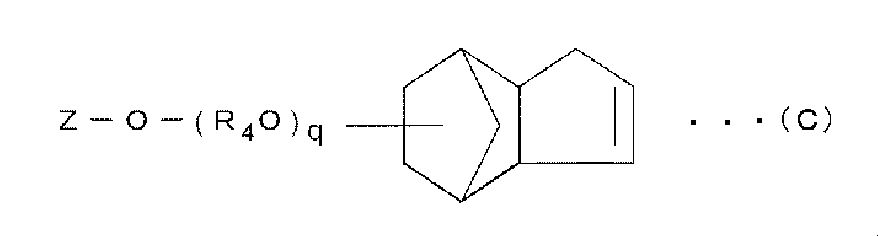
- dicyclopentenyloxyalkyl (meth) acrylate examples include (meth) acrylic monomers represented by the general formula (C).
- Z represents a (meth) acryloyl group
- R 4 represents an alkylene group having 1 to 4 carbon atoms
- q represents an integer of 1 to 20).
- Such (meth) acrylic monomers include dicyclopentenyloxyethyl (meth) acrylate, dicyclopentenyloxydiethylene glycol (meth) acrylate, dicyclopentenyloxytriethylene glycol (meth) acrylate, and dicyclopentenyloxypropylene glycol.
- (Meth) acrylate etc. are mentioned, These 1 type (s) or 2 or more types can be used. Among these, dicyclopentenyloxyethyl (meth) acrylate is preferable because it has good surface curability and can be easily obtained.
- R 4 is preferably an alkylene group having 1 to 4 carbon atoms, more preferably an ethylene group, from the viewpoint of high resin strength.
- q is preferably 1 to 3 and more preferably 1 in terms of the resin strength of the cured product.
- (1-4) (Meth) acrylate having an aromatic group examples include a (meth) acrylic monomer represented by the general formula (D).
- Z—O— (R 5 O) r —R 6 (D) (Wherein Z represents a (meth) acryloyl group, R 5 represents —C 2 H 4 —, —C 3 H 6 —, —CH 2 CH (CH 3 ) —, —C 4 H 8 — or —C 6 H 12 —, R 6 represents a phenyl group or a phenyl group having an alkyl group having 1 to 3 carbon atoms, and r represents an integer of 1 to 10)
- Such (meth) acrylic monomers include phenoxyethyl (meth) acrylate, phenoxydiethylene glycol (meth) acrylate, phenoxypolyethylene glycol (meth) acrylate, phenoxypropyl (meth) acrylate, phenoxydipropylene glycol (meth) acrylate and Phenoxy polypropylene glycol (meth) acrylate etc. are mentioned, These 1 type (s) or 2 or more types can be used. Among these, phenoxyethyl (meth) acrylate is preferable because of its great effect.
- (meth) acrylic monomer having a hydroxyl group examples include a (meth) acrylic monomer represented by the general formula (E).
- Z—O— (R 7 O) s —H (E) (Wherein Z represents a (meth) acryloyl group, R 7 represents —C 2 H 4 —, —C 3 H 6 —, —CH 2 CH (CH 3 ) —, —C 4 H 8 — or —C 6 H 12- represents, and s represents an integer of 1 to 10.)
- Examples of such (meth) acrylic monomers include hydroxyalkyl (meth) acrylates such as 2-hydroxyethyl (meth) acrylate, 2-hydroxypropyl (meth) acrylate, and hydroxybutyl (meth) acrylate. 1 type (s) or 2 or more types can be used. Among these, 2-hydroxyethyl (meth) acrylate and / or 2-hydroxypropyl (meth) acrylate are preferable because they are inexpensive and have good adhesiveness.
- (1-6) (meth) acrylic acid ester of higher alcohol, (1-7) (meth) acrylic acid ester of polyhydric alcohol, or (1-8) urethane having (meth) acryloyloxy group A prepolymer or the like can be used.
- the (meth) acrylic monomers it is preferable to contain (1-5) a (meth) acrylic monomer having a hydroxyl group in terms of great effect.
- the content ratio of the (meth) acrylic monomer having (1-5) hydroxyl group in the (meth) acrylic monomer is preferably 5 to 70 parts by mass in 100 parts by mass of the (meth) acrylic monomer. 60 parts by mass is more preferable.
- the combination of the following (X) or (Y) is preferable and the combination of (Y) is more preferable in terms of a large effect.
- (X) (1-1) Combination of alkyl (meth) acrylate, (1-3) dicyclopentenyloxyalkyl (meth) acrylate and (1-5) hydroxyalkyl (meth) acrylate Component (1-1), Component The content ratio of (1-3) and component (1-5) is 100 parts by mass in total of component (1-1), component (1-3) and component (1-5).
- 1-1): Component (1-3): Component (1-5) 40 to 90: 5 to 35: 5 to 35 is preferable, and 50 to 80:10 to 25:10 to 25 is more preferable.
- (Y) (1-2) Combination of (meth) acrylic acid monomer having bisphenol skeleton, (1-4) (meth) acrylate having aromatic group and (1-5) hydroxyalkyl (meth) acrylate Component (1 -2)
- the content ratio of the component (1-4) and the component (1-5) is the mass in the total of 100 parts by mass of the component (1-2), the component (1-4) and the component (1-5).
- the ratio of component (1-2): component (1-4): component (1-5) 1-20: 20-60: 30-70 is preferable, and 5-15: 30-55: 35-60 is preferable. More preferred.
- Component (2) is preferably used in an amount of 0.5 to 10 parts by weight, preferably 1 to 7 parts by weight per 100 parts by weight of component (1). If it is less than 0.5 parts by mass, the curing rate may be slow, and if it exceeds 10 parts by mass, the storage stability may be slow.
- curing accelerator examples include ⁇ -diketone chelates and / or ⁇ -ketoesters.
- ⁇ -diketone chelates include vanadyl acetylacetonate, cobalt acetylacetonate, and copper acetylacetonate.
- ⁇ -ketoester examples include vanadyl naphthenate, vanadyl stearate, copper naphthenate, cobalt octylate and the like, and one or more of these can be used.
- metal salts having reducibility are preferable, and one or more of the group consisting of vanadium acetylacetonate, copper naphthenate and cobalt octylate are used.
- vanadium acetylacetonate copper naphthenate
- cobalt octylate are used.
- vanadyl acetylacetonate is most preferred.
- Component (3) is preferably used in an amount of 0.05 to 5 parts by weight, more preferably 0.1 to 2 parts by weight, based on 100 parts by weight of component (1). If it is less than 0.05 parts by mass, the curing rate may be slow and the adhesiveness may be small. If it exceeds 5 parts by mass, unreacted components may remain and the adhesiveness may be reduced.
- the adhesive according to the embodiment of the present invention preferably uses an elastomer component in order to improve peel strength and impact strength.
- the elastomer include acrylonitrile-butadiene-methacrylic acid copolymer, acrylonitrile-butadiene-methacrylate copolymer, methyl methacrylate-butadiene-styrene copolymer, acrylonitrile-styrene-butadiene copolymer, acrylonitrile-butadiene rubber, wire
- elastomer components can be used alone or in combination of two or more if the compatibility is good.
- terminal (meth) acryl-modified polybutadiene can also be used.
- methyl methacrylate-butadiene-styrene copolymer and / or acrylonitrile-butadiene rubber are preferable, and their combined use is more preferable from the viewpoint of solubility and adhesion to (meth) acrylic monomers.
- Component (4) is preferably used in an amount of 5 to 35 parts by weight, more preferably 10 to 30 parts by weight, based on 100 parts by weight of component (1).
- the amount is less than 5 parts by mass, the viscosity and the adhesiveness may be lowered.
- the amount exceeds 35 parts by mass, the viscosity is too high and a problem may occur in the work.
- paraffins can be used for the adhesive according to the embodiment of the present invention in order to quickly cure the portion in contact with air.
- paraffins include paraffin wax, microcrystalline wax, carnauba wax, beeswax, lanolin, whale wax, ceresin and candelilla wax. These 1 type (s) or 2 or more types can be used.
- the amount of paraffin used is preferably 0.1 to 5 parts by mass, and more preferably 0.3 to 2.5 parts by mass with respect to 100 parts by mass of component (1). If the amount is less than 0.1 parts by mass, the portion in contact with the air may be hardened. If the amount exceeds 5 parts by mass, the adhesive strength may decrease.
- the adhesive according to the embodiment of the present invention can use various antioxidants including a polymerization inhibitor for the purpose of improving storage stability.
- Antioxidants include hydroquinone, hydroquinone monomethyl ether, 2,6-cytiary butyl-p-cresol, 2,2'-methylenebis (4-methyl-6-tertiary butylphenol), triphenyl phosphate, phenothiazine and N- Examples thereof include isopropyl-N′-phenyl-p-phenylenediamine, and one or more of these can be used.
- the amount of the polymerization inhibitor used is preferably 0.001 to 3 parts by mass, more preferably 0.01 to 1 part by mass with respect to 100 parts by mass of the component (1). If it is less than 0.001 part by mass, there may be no effect, and if it exceeds 3 parts by mass, the adhesive strength may decrease.
- the adhesive which concerns on embodiment of this invention can use a phosphate in order to improve adhesiveness.
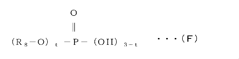
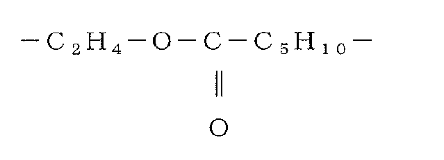
- the phosphate include a compound represented by the general formula (F). Wherein R 8 is CH 2 ⁇ CR 9 CO (OR 10 ) u — group (where R 9 is hydrogen or methyl group, R 10 is —C 2 H 4 —, —C 3 H 6 —, —CH 2 CH (CH 3 ) —, —C 4 H 8 —, —C 6 H 12 — or And u represents an integer of 1 to 10. ) And t represents an integer of 1 or 2)
- Examples of the phosphate include acid phosphooxyethyl (meth) acrylate, acid phosphooxypropyl (meth) acrylate, and bis (2- (meth) acryloyloxyethyl) phosphate. One or more of these may be used. Can be used. Among these, acid phosphooxyethyl (meth) acrylate is preferable because of its great effect.
- the amount of phosphate used is preferably 0.1 to 5 parts by mass, more preferably 0.2 to 1.0 part by mass, relative to 100 parts by mass of component (1). If the amount is less than 0.1 parts by mass, the adhesive strength may decrease. If the amount exceeds 5 parts by mass, the adhesive strength may decrease.
- thermoplastic polymers such as chlorosulfonated polyethylene, polyurethane, styrene-acrylonitrile copolymer and polymethyl methacrylate, fine powder silica, and the like may be used.
- Adhesive 1 Specific examples of the adhesive used in the embodiment of the present invention are shown in Table 1 (Adhesive 1) and Table 2 (Adhesive 2).
- Tables 1 and 2 methyl methacrylate, 2-hydroxyethyl methacrylate, dicyclopentenyloxyethyl methacrylate, cumene hydroperoxide, methyl methacrylate-butadiene-styrene copolymer (MMA-BD-ST copolymer), vanadyl acetyl As acetonate, 2-hydroxypropyl methacrylate, and phenoxyethyl methacrylate, commercially available products were used.
- MMA-BD-ST copolymer methyl methacrylate-butadiene-styrene copolymer
- vanadyl acetyl As acetonate 2-hydroxypropyl methacrylate
- phenoxyethyl methacrylate commercially available products were used.
- AN-BD rubber is a commercial product of high nitrile NBR
- paraffins is a commercial product of paraffin wax
- polymerization inhibitor is a commercial product of hydroquinone monomethyl ether.
- the adhesive used in the embodiment of the present invention is obtained by mixing the first agent containing the component (2) and the second agent containing the component (3).
- a two-component (meth) acrylic adhesive can be used.
- the two-agent type (meth) acrylic adhesive does not mix all the essential components of the adhesive composition of the present invention during storage, and the adhesive composition is divided into a first agent and a second agent.
- At least the component (2) can be stored separately, and at least the component (3) can be stored separately in the second agent. It is preferable to store the phosphate in the second agent.
- both agents can be applied to the semiconductor block 8 simultaneously or separately, and contacted and cured to be used as a two-component adhesive.
- one or both of the first agent and the second agent are preliminarily incorporated with a polymerizable vinyl monomer and other optional components, and both are mixed at the time of use, so that one-component adhesive is used.
- a polymerizable vinyl monomer and other optional components can be mixed at the time of use, so that one-component adhesive is used.
- the adhesive according to the embodiment of the present invention since the curing speed is faster than that of the epoxy adhesive or the like, the bonding time is short, and the working efficiency can be improved. Even when two-part adhesives are used, accurate measurement of the two parts is not required, and even incomplete measurement or mixing, the adhesive can be cured at normal temperature without deteriorating the energy, such as ultraviolet rays. There is no need to use. Furthermore, since the adhesive swells when immersed in warm water, the semiconductor block 8 and the base substrate 7 can be easily peeled off, and it is not necessary to use a liquid that is difficult to handle, such as an organic solvent.
- the temperature of the hot water for swelling the adhesive is preferably 30 to 150 ° C, more preferably 50 to 100 ° C, and further preferably 65 to 80 ° C.
- step S101 in FIG. 10 a semiconductor ingot such as Si is cut into a block shape having a predetermined size (for example, 156 ⁇ 156 ⁇ 200 mm) to obtain a plurality of semiconductor blocks 8.
- the semiconductor block 8 is subjected to surface processing by brush polishing or the like.
- step S103 the base substrate 7 is bonded to the semiconductor block 8 according to the method shown in the flowchart of FIG. 8, and the semiconductor block 10 with the base substrate shown in FIG. 9A is manufactured.
- step S105 as shown in FIG. 9B, the wire is advanced from the surface of the semiconductor block 8 to about half of the adhesive layer 9 by the wire saw device, and the semiconductor block 8 is cut into a plurality of thin plates.
- step S107 the cutting fluid (slurry) used for cutting is washed.
- step S109 the cut semiconductor block 10 with the base substrate is immersed in warm water 100 to swell the adhesive layer 9 and peel off the base substrate 7 and the semiconductor block 8 as shown in FIG. 9C. To do. A plurality of thin plates obtained by peeling are dried, and after a predetermined inspection in step S111, they are shipped as semiconductor wafers in step S113. The obtained semiconductor wafer is used for a semiconductor integrated circuit or a solar cell substrate.
- a semiconductor wafer was manufactured using the semiconductor block bonding apparatus of the present invention.
- Five suction pads 32 and five actuators 33 were suspended from the support 31.
- As the semiconductor block a 156 ⁇ 156 ⁇ 200 mm cubic silicon ingot was used. Two types of adhesives, adhesive 1 and adhesive 2, were used.
- the semiconductor block was cut by a wire saw device so as to obtain a thin plate having a thickness of 200 ⁇ m. Tap water was used as the cutting fluid (slurry).
- the semiconductor block with the base substrate after cutting was immersed in warm water at 70 ° C. to obtain a semiconductor wafer.
- the semiconductor block bonding apparatus according to the present invention can be automated and the manufacturing efficiency of the semiconductor wafer can be improved regardless of which one of the adhesive 1 and the adhesive 2 is used.
- the obtained semiconductor wafer was in a quality state usable for a semiconductor integrated circuit or a solar cell substrate.
- the base substrate 7 is conveyed into the apparatus.
- a removable stage (jig) 13 is further attached to the conveying member 12.
- the transport order of the semiconductor block 8 and the base substrate 7 can be reversed. 1 discloses a method of moving the suction pad 32 up and down using an actuator 33 such as an air cylinder. Instead of the support portion of FIG. It is also possible to suspend the semiconductor block 8 by manually attaching the block adsorbing member to the tip of the wire. Furthermore, a detection instrument that detects the physical state of the adhesive may be provided in the container that stores the adhesive in the application unit 4.
Landscapes
- Adhesives Or Adhesive Processes (AREA)
- Processing Of Stones Or Stones Resemblance Materials (AREA)
- Mechanical Treatment Of Semiconductor (AREA)
Abstract
Description
図1~2に示すように、本発明の実施の形態に係る半導体ブロック接着装置1は、半導体ブロック8及び下地基板7の搬入及び搬出を行う搬入出部2と、半導体ブロック8を支持し、半導体ブロック8を上下に移動させる支持部3と、接着剤を下地基板7上に塗布する塗布部4と、制御装置5と、表示装置6とを備える。
次に、図1~図7の概略図及び図8のフローチャートを用いて、実施の形態に係る半導体ブロック接着方法を説明する。
本発明の実施の形態に用いられる接着剤は、重合性ビニルモノマーを含む接着剤を用いるのが好ましく、特に、(1)(メタ)アクリル系モノマー、(2)重合開始剤、(3)硬化促進剤、及び(4)エラストマーを含む(メタ)アクリル系接着剤を用いることができる。
(メタ)アクリル系モノマーとは、(メタ)アクリル酸及び/又は(メタ)アクリル酸エステルから選ばれるアクリル系化合物という。(メタ)アクリル系モノマーとしては、以下のものが挙げられる。
アルキル(メタ)アクリレートとしては、一般式(A)で示される(メタ)アクリル系モノマー等が挙げられる。
Z-O-R1 ・・・(A)
(式中、Zは(メタ)アクリロイル基を示し、R1は炭素数1~10のアルキル基を表す。)
ビスフェノール骨格を有する(メタ)アクリル酸モノマーとしては、一般式(B)で示される(メタ)アクリル系モノマー等が挙げられる。

ジシクロペンテニルオキシアルキレン(メタ)アクリレートとしては、一般式(C)で示される(メタ)アクリル系モノマー等が挙げられる。
芳香族基を有する(メタ)アクリレートとしては、一般式(D)で示される(メタ)アクリル系モノマー等が挙げられる。
Z-O-(R5O)r-R6 ・・・(D)
(式中、Zは(メタ)アクリロイル基を示し、R5は-C2H4-、-C3H6-、-CH2CH(CH3)-、-C4H8-又は-C6H12-を示し、R6はフェニル基又は炭素数1~3のアルキル基を有するフェニル基を示し、rは1~10の整数を示す。)
ヒドロキシル基を有する(メタ)アクリル系モノマーとしては、一般式(E)で示される(メタ)アクリル系モノマー等が挙げられる。
Z-O-(R7O)s-H ・・・(E)
(式中、Zは(メタ)アクリロイル基を示し、R7は-C2H4-、-C3H6-、-CH2CH(CH3)-、-C4H8-又は-C6H12-を示し、sは1~10の整数を示す。)
成分(1-1)、成分(1-3)及び成分(1-5)の含有割合は、成分(1-1)、成分(1-3)及び成分(1-5)の合計100質量部中、質量比で、成分(1-1):成分(1-3):成分(1-5)=40~90:5~35:5~35が好ましく、50~80:10~25:10~25がより好ましい。
成分(1-2)、成分(1-4)及び成分(1-5)の含有割合は、成分(1-2)、成分(1-4)及び成分(1-5)の合計100質量部中、質量比で、成分(1-2):成分(1-4):成分(1-5)=1~20:20~60:30~70が好ましく、5~15:30~55:35~60がより好ましい。
重合開始剤としては、クメンハイドロパーオキサイド、パラメンタンハイドロパーオキサイド、ターシャリーブチルハイドロパーオキサイド、ジイソプロピルベンゼンジハイドロパーオキサイド、メチルエチルケトンパーオキサイド、ベンゾイルパーオキサイド及びターシャリーブチルパーオキシベンゾエート等の有機過酸化物が好ましく、これらの1種又は2種以上が使用できる。これらの中では成分(3)や成分(4)との反応性の点で、クメンハイドロパーオキサイドが好ましい。
硬化促進剤としては、β-ジケトンキレート及び/又はβ-ケトエステルが挙げられる。β-ジケトンキレートとしては、バナジルアセチルアセトネート、コバルトアセチルアセトネートオ及び銅アセチルアセトネート等が挙げられる。β-ケトエステルとしては、ナフテン酸バナジル、ステアリン酸バナジル、ナフテン酸銅若しくはオクチル酸コバルト等が挙げられ、これらの1種又は2種以上が使用できる。これらの中では、成分(2)との反応性の点で、還元性を有する金属塩が好ましく、バナジウムアセチルアセトネート、ナフテン酸銅及びオクチル酸コバルトからなる群のうちの1種又は2種以上がより好ましく、バナジルアセチルアセトネートが最も好ましい。
本発明の実施の形態に係る接着剤は、剥離強度と衝撃強度を向上させるためにエラストマー成分を使用することが好ましい。エラストマーとしては、アクリロニトリル-ブタジエン-メタクリル酸共重合体、アクリロニトリル-ブタジエン-メタクリレート共重合体、メチルメタクリレート-ブタジエン-スチレン共重合体、アクリロニトリル-スチレン-ブタジエン共重合体、並びに、アクリロニトリル-ブタジエンゴム、線状ポリウレタン、スチレン-ブタジエンゴム、クロロプレンゴム及びブタジエンゴム等の各種合成ゴム、天然ゴム、スチレン-ポリブタジエン-スチレン系合成ゴムといったスチレン系熱可塑性エラストマー、ポリエチレン-EPDM合成ゴムといったオレフィン系熱可塑性エラストマー、並びにカプロラクトン型、アジペート型及びPTMG型といったウレタン系熱可塑性エラストマー、ポリブチレンテレフタレート-ポリテトラメチレングリコールマルチブロックポリマーといったポリエステル系熱可塑性エラストマー、ナイロン-ポリオールブロック共重合体といったポリアミド系熱可塑性エラストマー、1,2-ポリブタジエン系熱可塑性エラストマー、並びに塩ビ系熱可塑性エラストマー等が挙げられる。これらのエラストマー成分は相溶性が良ければ、1種又は2種以上を使用することができる。又、末端(メタ)アクリル変性したポリブタジエンも使用できる。これらの中では、(メタ)アクリル系モノマーに対する溶解性や接着性の点で、メチルメタクリレート-ブタジエン-スチレン共重合体及び/又はアクリロニトリル-ブタジエンゴムが好ましく、その併用がより好ましい。
本発明の実施の形態に係る接着剤は、空気に接している部分の硬化を迅速にするために各種パラフィン類を使用することができる。パラフィン類としては、パラフィンワックス、マイクロクリスタリンワックス、カルナバろう、蜜ろう、ラノリン、鯨ろう、セレシン及びカンデリラろう等が挙げられる。これらの1種又は2種以上を使用することができる。
パラフィン類の使用量は、成分(1)100質量部に対して、0.1~5質量部が好ましく、0.3~2.5質量部がより好ましい。0.1質量部未満では空気に接している部分の硬化が悪くなる場合があり、5質量部を超えると接着強度が低下する場合がある。


本発明の実施の形態に係る半導体ウエハの製造方法について、図9(a)~図9(c)の概略図及び図10のフローチャートを用いて説明する。
本発明は上記の実施の形態によって記載したが、この開示の一部をなす論述及び図面はこの発明を限定するものではない。この開示から当業者には様々な代替実施の形態、実施例及び運用技術が明らかとなろう。
2…搬入出部
3…支持部
4…塗布部
5…制御装置
6…表示装置
7…下地基板
8…半導体ブロック
9…接着剤層
10…下地基板付き半導体ブロック
11…架台
12…搬送部材
13…ステージ
21…ガイド
31…支柱部
32…吸着パッド
33…アクチュエータ
34…エア機器
41…支柱部
42…シリンジ
43…ディスペンサ
51…ステージ制御部
52…ブロック昇降制御部
53…ディスペンサ制御部
Claims (18)
- 半導体ブロック及び下地基板の搬入及び搬出を行う搬入出部と、
前記半導体ブロック表面に吸着する吸着パッド、前記吸着パッドに接続され、前記吸着パッドに吸着された前記半導体ブロックを空気圧により上下に移動させるアクチュエータ、及び前記アクチュエータに接続されたエア機器を備える支持部と、
重合性ビニルモノマーを含む接着剤を前記下地基板上に塗布する塗布部と、
前記半導体ブロック又は前記下地基板を載せ、前記搬入出部、前記支持部及び前記塗布部間を移動するステージと、
前記塗布部において前記下地基板上に前記接着剤を塗布した後に塗布後の下地基板を前記半導体ブロックの下方へ搬送し、前記半導体ブロックを下方に降ろして前記下地基板と接着させる工程を制御する制御装置と、
を備えることを特徴とする半導体ブロック接着装置。 - 前記アクチュエータが、エアシリンダーである請求項1に記載の半導体ブロック接着装置。
- 前記搬入出部が、前記半導体ブロックを前記ステージ上の所定位置に固定するガイドを備える請求項1又は2に記載の半導体ブロック接着装置。
- 前記塗布部が、前記接着剤を混合するスタティックミキサーを備える請求項1~3のいずれか1項に記載の半導体ブロック接着装置。
- 前記接着剤が、(1)(メタ)アクリル系モノマー、(2)重合開始剤、(3)硬化促進剤、及び(4)エラストマーを含む(メタ)アクリル系接着剤である請求項1~4のいずれか1項に記載の半導体ブロック接着装置。
- 前記接着剤が、前記成分(2)を含む第1剤と、前記成分(3)を含む第2剤とを混合して得られる2剤型(メタ)アクリル系接着剤である請求項5に記載の半導体ブロック接着装置。
- 前記成分(1)が、ヒドロキシアクリル(メタ)アクリレートを含む請求項5に記載の半導体ブロック接着装置。
- 前記成分(2)が、クメンハイドロパーオキサイド、パラメンタンハイドロパーオキサイド、ターシャリーブチルハイドロパーオキサイド、ジイソプロピルベンゼンジハイドロパーオキサイド、メチルエチルケトンパーオキサイド、ベンゾイルパーオキサイド及びターシャリーブチルパーオキシベンゾエート及びこれらの組み合わせよりなる群から選択される請求項5~7のいずれか1項に記載の半導体ブロック接着装置。
- 前記成分(3)が、β-ジケトンキレート及び/又はβ―ケトエステルである請求項5~8のいずれか1項に記載の半導体ブロック接着装置。
- 前記接着剤が、(1)(メタ)アクリル系モノマー100質量部に対して、成分(2)を0.5~10質量部、成分(3)を0.05~5質量部、成分(4)を5~35質量部含む請求項5~9のいずれか1項に記載の半導体ブロック接着装置。
- 搬入出部と、支持部と、塗布部と、半導体ブロック又は下地基板を搬送するためのステージとを備える半導体ブロック接着装置を用いた半導体ブロック接着方法であって、
半導体ブロックを前記ステージ上に載せ、前記半導体ブロックを前記搬入出部から前記支持部に搬送するステップと、
前記支持部において前記半導体ブロックを前記ステージの上方へ持ち上げるステップと、
前記ステージを前記支持部から前記搬入出部に戻し、前記ステージ上に下地基板を載せるステップと、
前記下地基板を載せた前記ステージを前記搬入出部から前記塗布部へ搬送するステップと、
前記塗布部において、前記下地基板上に重合性ビニルモノマーを含む接着剤を塗布するステップと、
塗布後の前記下地基板を載せた前記ステージを前記塗布部から前記支持部へ搬送し、接着剤が塗布された前記下地基板上に前記半導体ブロックを載せ、前記下地基板と前記半導体ブロックとを接着するステップと、
接着後の半導体ブロックを、前記支持部から前記搬入出部へ搬送するステップと
を含む半導体ブロック接着方法。 - 前記接着剤が、(1)(メタ)アクリル系モノマー、(2)重合開始剤、(3)硬化促進剤、及び(4)エラストマーを含む(メタ)アクリル系接着剤である請求項11に記載の半導体ブロック接着方法。
- 前記接着剤が、前記成分(2)を含む第1剤と、前記成分(3)を含む第2剤とを混合して得られる2剤型(メタ)アクリル系接着剤である請求項12に記載の半導体ブロック接着方法。
- 前記成分(1)が、ヒドロキシアクリル(メタ)アクリレートを含む請求項12に記載の半導体ブロック接着方法。
- 前記成分(2)が、クメンハイドロパーオキサイド、パラメンタンハイドロパーオキサイド、ターシャリーブチルハイドロパーオキサイド、ジイソプロピルベンゼンジハイドロパーオキサイド、メチルエチルケトンパーオキサイド、ベンゾイルパーオキサイド及びターシャリーブチルパーオキシベンゾエート及びこれらの組み合わせよりなる群から選択される請求項12~14のいずれか1項に記載の半導体ブロック接着方法。
- 前記成分(3)が、β-ジケトンキレート及び/又はβ―ケトエステルである請求項12~15のいずれか1項に記載の半導体ブロック接着方法。
- 前記接着剤が、(1)(メタ)アクリル系モノマー100質量部に対して、成分(2)を0.5~10質量部、成分(3)を0.05~5質量部、成分(4)を5~35質量部含む請求項12~16に記載の半導体ブロック接着方法。
- 請求項11~17のいずれか1項の接着方法により得られる下地基板付き半導体ブロックを複数の薄板状に切断し、
切断後の前記下地基板付き半導体ブロックを温水中に浸漬し、
前記温水中において前記下地基板と前記半導体ブロックとを剥離する
ことを特徴とする半導体ウエハの製造方法。
Priority Applications (3)
| Application Number | Priority Date | Filing Date | Title |
|---|---|---|---|
| JP2012500597A JP5847698B2 (ja) | 2010-02-16 | 2011-02-15 | 半導体ブロック接着装置、半導体ブロック接着方法及び半導体ウエハの製造方法 |
| CN201180009787.2A CN102763195B (zh) | 2010-02-16 | 2011-02-15 | 半导体区块粘接装置、半导体区块粘接方法及半导体晶片的制造方法 |
| KR1020127023943A KR20130007569A (ko) | 2010-02-16 | 2011-02-15 | 반도체 블록 접착장치, 반도체 블록 접착방법 및 반도체 웨이퍼의 제조방법 |
Applications Claiming Priority (2)
| Application Number | Priority Date | Filing Date | Title |
|---|---|---|---|
| JP2010-031598 | 2010-02-16 | ||
| JP2010031598 | 2010-02-16 |
Publications (1)
| Publication Number | Publication Date |
|---|---|
| WO2011102341A1 true WO2011102341A1 (ja) | 2011-08-25 |
Family
ID=44482926
Family Applications (1)
| Application Number | Title | Priority Date | Filing Date |
|---|---|---|---|
| PCT/JP2011/053153 Ceased WO2011102341A1 (ja) | 2010-02-16 | 2011-02-15 | 半導体ブロック接着装置、半導体ブロック接着方法及び半導体ウエハの製造方法 |
Country Status (5)
| Country | Link |
|---|---|
| JP (1) | JP5847698B2 (ja) |
| KR (1) | KR20130007569A (ja) |
| CN (1) | CN102763195B (ja) |
| TW (1) | TWI515781B (ja) |
| WO (1) | WO2011102341A1 (ja) |
Cited By (3)
| Publication number | Priority date | Publication date | Assignee | Title |
|---|---|---|---|---|
| JP2013071225A (ja) * | 2011-09-29 | 2013-04-22 | Fujikoshi Mach Corp | インゴットへの切り代プレートおよび取付プレートの接着方法および接着装置 |
| JP2013138194A (ja) * | 2011-12-01 | 2013-07-11 | Denki Kagaku Kogyo Kk | 被加工部材の仮固定方法 |
| WO2017018486A1 (ja) * | 2015-07-30 | 2017-02-02 | デンカ株式会社 | 組成物 |
Families Citing this family (5)
| Publication number | Priority date | Publication date | Assignee | Title |
|---|---|---|---|---|
| TWI514460B (zh) * | 2014-08-22 | 2015-12-21 | Sino American Silicon Prod Inc | 晶圓製作方法 |
| US10631450B2 (en) * | 2015-07-10 | 2020-04-21 | Yamaha Hatsudoki Kabushiki Kaisha | Component mounting system, component mounter and component mounting method |
| CN105835248A (zh) * | 2016-05-30 | 2016-08-10 | 深圳市创世纪机械有限公司 | 一种玻璃机夹具 |
| CN108039122B (zh) * | 2017-12-29 | 2019-08-30 | 深圳市华星光电半导体显示技术有限公司 | 一种柔性显示器的制备方法及柔性显示器 |
| US10515569B2 (en) | 2017-12-29 | 2019-12-24 | Shenzhen China Star Optoelectronics Semiconductor Display Technology Co., Ltd. | Preparation method of flexible display and flexible display |
Citations (8)
| Publication number | Priority date | Publication date | Assignee | Title |
|---|---|---|---|---|
| JPS5918773A (ja) * | 1982-07-22 | 1984-01-31 | Denki Kagaku Kogyo Kk | 接着剤組成物 |
| JPS5925855A (ja) * | 1982-08-03 | 1984-02-09 | Denki Kagaku Kogyo Kk | 接着剤組成物 |
| JP2000208449A (ja) * | 1999-01-12 | 2000-07-28 | Mitsubishi Materials Corp | ウェ―ハの剥離方法および剥離装置 |
| JP2003205517A (ja) * | 2002-01-15 | 2003-07-22 | Nippei Toyama Corp | シリコンインゴットに対する取付ステー接着装置及び接着方法 |
| JP2006188627A (ja) * | 2005-01-07 | 2006-07-20 | Okura Ind Co Ltd | 二液主剤型アクリル系接着剤用b剤 |
| JP2009018265A (ja) * | 2007-07-12 | 2009-01-29 | Railway Technical Res Inst | 二液接触型非混合塗布ノズル及びそれを用いた二液型接着剤の塗布方法並びにアンカーボルトの固定方法 |
| JP2009114455A (ja) * | 2004-03-11 | 2009-05-28 | Hiroshi Okai | 反応性ホットメルト硬化性組成物の製造方法並びに塗布装置 |
| JP2009295895A (ja) * | 2008-06-09 | 2009-12-17 | Sumitomo Bakelite Co Ltd | 回路板用導電性ペースト |
Family Cites Families (4)
| Publication number | Priority date | Publication date | Assignee | Title |
|---|---|---|---|---|
| JPH11186199A (ja) * | 1997-12-17 | 1999-07-09 | Tokyo Seimitsu Co Ltd | インゴットマウント装置 |
| JP4388362B2 (ja) * | 2003-12-22 | 2009-12-24 | 京セラ株式会社 | 半導体インゴットの切断方法 |
| WO2007148506A1 (ja) * | 2006-06-19 | 2007-12-27 | Denki Kagaku Kogyo Kabushiki Kaisha | 樹脂組成物及びそれを用いる被加工部材の仮固定方法と表面保護方法 |
| KR100917406B1 (ko) * | 2009-07-03 | 2009-09-14 | 다이섹(주) | 태양전지 잉곳용 스퀘어 컷팅장치 |
-
2011
- 2011-02-15 KR KR1020127023943A patent/KR20130007569A/ko not_active Withdrawn
- 2011-02-15 JP JP2012500597A patent/JP5847698B2/ja not_active Expired - Fee Related
- 2011-02-15 WO PCT/JP2011/053153 patent/WO2011102341A1/ja not_active Ceased
- 2011-02-15 CN CN201180009787.2A patent/CN102763195B/zh not_active Expired - Fee Related
- 2011-02-16 TW TW100105113A patent/TWI515781B/zh not_active IP Right Cessation
Patent Citations (8)
| Publication number | Priority date | Publication date | Assignee | Title |
|---|---|---|---|---|
| JPS5918773A (ja) * | 1982-07-22 | 1984-01-31 | Denki Kagaku Kogyo Kk | 接着剤組成物 |
| JPS5925855A (ja) * | 1982-08-03 | 1984-02-09 | Denki Kagaku Kogyo Kk | 接着剤組成物 |
| JP2000208449A (ja) * | 1999-01-12 | 2000-07-28 | Mitsubishi Materials Corp | ウェ―ハの剥離方法および剥離装置 |
| JP2003205517A (ja) * | 2002-01-15 | 2003-07-22 | Nippei Toyama Corp | シリコンインゴットに対する取付ステー接着装置及び接着方法 |
| JP2009114455A (ja) * | 2004-03-11 | 2009-05-28 | Hiroshi Okai | 反応性ホットメルト硬化性組成物の製造方法並びに塗布装置 |
| JP2006188627A (ja) * | 2005-01-07 | 2006-07-20 | Okura Ind Co Ltd | 二液主剤型アクリル系接着剤用b剤 |
| JP2009018265A (ja) * | 2007-07-12 | 2009-01-29 | Railway Technical Res Inst | 二液接触型非混合塗布ノズル及びそれを用いた二液型接着剤の塗布方法並びにアンカーボルトの固定方法 |
| JP2009295895A (ja) * | 2008-06-09 | 2009-12-17 | Sumitomo Bakelite Co Ltd | 回路板用導電性ペースト |
Cited By (6)
| Publication number | Priority date | Publication date | Assignee | Title |
|---|---|---|---|---|
| JP2013071225A (ja) * | 2011-09-29 | 2013-04-22 | Fujikoshi Mach Corp | インゴットへの切り代プレートおよび取付プレートの接着方法および接着装置 |
| JP2013138194A (ja) * | 2011-12-01 | 2013-07-11 | Denki Kagaku Kogyo Kk | 被加工部材の仮固定方法 |
| WO2017018486A1 (ja) * | 2015-07-30 | 2017-02-02 | デンカ株式会社 | 組成物 |
| CN107922520A (zh) * | 2015-07-30 | 2018-04-17 | 电化株式会社 | 组合物 |
| US10647889B2 (en) | 2015-07-30 | 2020-05-12 | Denka Company Limited | Adhesive composition |
| CN107922520B (zh) * | 2015-07-30 | 2020-08-04 | 电化株式会社 | 组合物 |
Also Published As
| Publication number | Publication date |
|---|---|
| KR20130007569A (ko) | 2013-01-18 |
| TW201201262A (en) | 2012-01-01 |
| CN102763195B (zh) | 2015-04-22 |
| JPWO2011102341A1 (ja) | 2013-06-17 |
| JP5847698B2 (ja) | 2016-01-27 |
| TWI515781B (zh) | 2016-01-01 |
| CN102763195A (zh) | 2012-10-31 |
Similar Documents
| Publication | Publication Date | Title |
|---|---|---|
| JP5847698B2 (ja) | 半導体ブロック接着装置、半導体ブロック接着方法及び半導体ウエハの製造方法 | |
| JP5466477B2 (ja) | 仮固定用接着剤組成物 | |
| CN106414635B (zh) | 粘接剂组合物以及使用粘接剂组合物的构件的暂时固定方法 | |
| CN101681823B (zh) | 半导体晶片磨削方法和在其中使用的树脂组合物以及保护片 | |
| CN101213225B (zh) | 固化性组合物以及使用该组合物的构件的暂时固定方法 | |
| JP6016793B2 (ja) | 仮固定用接着剤組成物 | |
| WO2013172353A1 (ja) | 積層体の加工装置及び加工方法 | |
| JP6443337B2 (ja) | 光硬化性組成物 | |
| JP6052869B2 (ja) | 被加工部材の仮固定方法 | |
| TW201317129A (zh) | 硬質基板積層體之加工方法及緊固夾具 | |
| TWI540659B (zh) | A semiconductor block bonding apparatus, a semiconductor block bonding method, and a method of manufacturing a semiconductor wafer | |
| JPWO2013084953A1 (ja) | 透光性硬質基板積層体の製造方法 | |
| JP2007161871A (ja) | 硬化性組成物及びそれを用いる部材の仮固定方法 | |
| JP5164316B2 (ja) | 接着剤及びそれを用いる部材の仮固定方法 | |
| KR102709092B1 (ko) | 연마장치용 정반, 연마장치 및 연마방법 | |
| CN104045240A (zh) | 硬质基板层叠体的加工方法及紧固夹具 | |
| JP2017206398A (ja) | 透光性硬質基板積層体の製造方法 | |
| JP2017214477A (ja) | 組成物 | |
| JP2002158199A (ja) | クリーニング機能付搬送部材の製造方法、及びそれに用いるクリーニングシート | |
| JP2007284620A (ja) | 粘着剤層、その製造方法、粘着シート、クリーニングシート、クリーニング機能付き搬送部材およびクリーニング方法 | |
| JP2003190884A (ja) | クリーニング機能付ラベルシート | |
| JP2005191532A (ja) | 半導体チップの製造方法 |
Legal Events
| Date | Code | Title | Description |
|---|---|---|---|
| WWE | Wipo information: entry into national phase |
Ref document number: 201180009787.2 Country of ref document: CN |
|
| 121 | Ep: the epo has been informed by wipo that ep was designated in this application |
Ref document number: 11744627 Country of ref document: EP Kind code of ref document: A1 |
|
| NENP | Non-entry into the national phase |
Ref country code: DE |
|
| WWE | Wipo information: entry into national phase |
Ref document number: 2012500597 Country of ref document: JP |
|
| ENP | Entry into the national phase |
Ref document number: 20127023943 Country of ref document: KR Kind code of ref document: A |
|
| 122 | Ep: pct application non-entry in european phase |
Ref document number: 11744627 Country of ref document: EP Kind code of ref document: A1 |