WO2011102064A1 - n型半導体層上の電極の形成方法 - Google Patents
n型半導体層上の電極の形成方法 Download PDFInfo
- Publication number
- WO2011102064A1 WO2011102064A1 PCT/JP2010/073768 JP2010073768W WO2011102064A1 WO 2011102064 A1 WO2011102064 A1 WO 2011102064A1 JP 2010073768 W JP2010073768 W JP 2010073768W WO 2011102064 A1 WO2011102064 A1 WO 2011102064A1
- Authority
- WO
- WIPO (PCT)
- Prior art keywords
- semiconductor layer
- type semiconductor
- electrode
- forming
- resist
- Prior art date
- Legal status (The legal status is an assumption and is not a legal conclusion. Google has not performed a legal analysis and makes no representation as to the accuracy of the status listed.)
- Ceased
Links
Images



Classifications
-
- H—ELECTRICITY
- H10—SEMICONDUCTOR DEVICES; ELECTRIC SOLID-STATE DEVICES NOT OTHERWISE PROVIDED FOR
- H10D—INORGANIC ELECTRIC SEMICONDUCTOR DEVICES
- H10D64/00—Electrodes of devices having potential barriers
- H10D64/01—Manufacture or treatment
- H10D64/011—Manufacture or treatment of electrodes ohmically coupled to a semiconductor
- H10D64/0116—Manufacture or treatment of electrodes ohmically coupled to a semiconductor to Group III-V semiconductors
-
- G—PHYSICS
- G03—PHOTOGRAPHY; CINEMATOGRAPHY; ANALOGOUS TECHNIQUES USING WAVES OTHER THAN OPTICAL WAVES; ELECTROGRAPHY; HOLOGRAPHY
- G03F—PHOTOMECHANICAL PRODUCTION OF TEXTURED OR PATTERNED SURFACES, e.g. FOR PRINTING, FOR PROCESSING OF SEMICONDUCTOR DEVICES; MATERIALS THEREFOR; ORIGINALS THEREFOR; APPARATUS SPECIALLY ADAPTED THEREFOR
- G03F7/00—Photomechanical, e.g. photolithographic, production of textured or patterned surfaces, e.g. printing surfaces; Materials therefor, e.g. comprising photoresists; Apparatus specially adapted therefor
- G03F7/004—Photosensitive materials
-
- G—PHYSICS
- G03—PHOTOGRAPHY; CINEMATOGRAPHY; ANALOGOUS TECHNIQUES USING WAVES OTHER THAN OPTICAL WAVES; ELECTROGRAPHY; HOLOGRAPHY
- G03F—PHOTOMECHANICAL PRODUCTION OF TEXTURED OR PATTERNED SURFACES, e.g. FOR PRINTING, FOR PROCESSING OF SEMICONDUCTOR DEVICES; MATERIALS THEREFOR; ORIGINALS THEREFOR; APPARATUS SPECIALLY ADAPTED THEREFOR
- G03F7/00—Photomechanical, e.g. photolithographic, production of textured or patterned surfaces, e.g. printing surfaces; Materials therefor, e.g. comprising photoresists; Apparatus specially adapted therefor
- G03F7/004—Photosensitive materials
- G03F7/0047—Photosensitive materials characterised by additives for obtaining a metallic or ceramic pattern, e.g. by firing
-
- G—PHYSICS
- G03—PHOTOGRAPHY; CINEMATOGRAPHY; ANALOGOUS TECHNIQUES USING WAVES OTHER THAN OPTICAL WAVES; ELECTROGRAPHY; HOLOGRAPHY
- G03F—PHOTOMECHANICAL PRODUCTION OF TEXTURED OR PATTERNED SURFACES, e.g. FOR PRINTING, FOR PROCESSING OF SEMICONDUCTOR DEVICES; MATERIALS THEREFOR; ORIGINALS THEREFOR; APPARATUS SPECIALLY ADAPTED THEREFOR
- G03F7/00—Photomechanical, e.g. photolithographic, production of textured or patterned surfaces, e.g. printing surfaces; Materials therefor, e.g. comprising photoresists; Apparatus specially adapted therefor
- G03F7/20—Exposure; Apparatus therefor
- G03F7/2002—Exposure; Apparatus therefor with visible light or UV light, through an original having an opaque pattern on a transparent support, e.g. film printing, projection printing; by reflection of visible or UV light from an original such as a printed image
-
- H—ELECTRICITY
- H01—ELECTRIC ELEMENTS
- H01S—DEVICES USING THE PROCESS OF LIGHT AMPLIFICATION BY STIMULATED EMISSION OF RADIATION [LASER] TO AMPLIFY OR GENERATE LIGHT; DEVICES USING STIMULATED EMISSION OF ELECTROMAGNETIC RADIATION IN WAVE RANGES OTHER THAN OPTICAL
- H01S5/00—Semiconductor lasers
- H01S5/04—Processes or apparatus for excitation, e.g. pumping, e.g. by electron beams
- H01S5/042—Electrical excitation ; Circuits therefor
- H01S5/0425—Electrodes, e.g. characterised by the structure
- H01S5/04252—Electrodes, e.g. characterised by the structure characterised by the material
-
- H—ELECTRICITY
- H10—SEMICONDUCTOR DEVICES; ELECTRIC SOLID-STATE DEVICES NOT OTHERWISE PROVIDED FOR
- H10D—INORGANIC ELECTRIC SEMICONDUCTOR DEVICES
- H10D62/00—Semiconductor bodies, or regions thereof, of devices having potential barriers
- H10D62/80—Semiconductor bodies, or regions thereof, of devices having potential barriers characterised by the materials
- H10D62/85—Semiconductor bodies, or regions thereof, of devices having potential barriers characterised by the materials being Group III-V materials, e.g. GaAs
- H10D62/8503—Nitride Group III-V materials, e.g. AlN or GaN
-
- H—ELECTRICITY
- H10—SEMICONDUCTOR DEVICES; ELECTRIC SOLID-STATE DEVICES NOT OTHERWISE PROVIDED FOR
- H10D—INORGANIC ELECTRIC SEMICONDUCTOR DEVICES
- H10D64/00—Electrodes of devices having potential barriers
- H10D64/01—Manufacture or treatment
- H10D64/011—Manufacture or treatment of electrodes ohmically coupled to a semiconductor
-
- H—ELECTRICITY
- H10—SEMICONDUCTOR DEVICES; ELECTRIC SOLID-STATE DEVICES NOT OTHERWISE PROVIDED FOR
- H10H—INORGANIC LIGHT-EMITTING SEMICONDUCTOR DEVICES HAVING POTENTIAL BARRIERS
- H10H20/00—Individual inorganic light-emitting semiconductor devices having potential barriers, e.g. light-emitting diodes [LED]
- H10H20/01—Manufacture or treatment
- H10H20/032—Manufacture or treatment of electrodes
-
- H—ELECTRICITY
- H10—SEMICONDUCTOR DEVICES; ELECTRIC SOLID-STATE DEVICES NOT OTHERWISE PROVIDED FOR
- H10H—INORGANIC LIGHT-EMITTING SEMICONDUCTOR DEVICES HAVING POTENTIAL BARRIERS
- H10H20/00—Individual inorganic light-emitting semiconductor devices having potential barriers, e.g. light-emitting diodes [LED]
- H10H20/80—Constructional details
- H10H20/83—Electrodes
- H10H20/832—Electrodes characterised by their material
-
- G—PHYSICS
- G03—PHOTOGRAPHY; CINEMATOGRAPHY; ANALOGOUS TECHNIQUES USING WAVES OTHER THAN OPTICAL WAVES; ELECTROGRAPHY; HOLOGRAPHY
- G03F—PHOTOMECHANICAL PRODUCTION OF TEXTURED OR PATTERNED SURFACES, e.g. FOR PRINTING, FOR PROCESSING OF SEMICONDUCTOR DEVICES; MATERIALS THEREFOR; ORIGINALS THEREFOR; APPARATUS SPECIALLY ADAPTED THEREFOR
- G03F7/00—Photomechanical, e.g. photolithographic, production of textured or patterned surfaces, e.g. printing surfaces; Materials therefor, e.g. comprising photoresists; Apparatus specially adapted therefor
- G03F7/004—Photosensitive materials
- G03F7/0045—Photosensitive materials with organic non-macromolecular light-sensitive compounds not otherwise provided for, e.g. dissolution inhibitors
-
- G—PHYSICS
- G03—PHOTOGRAPHY; CINEMATOGRAPHY; ANALOGOUS TECHNIQUES USING WAVES OTHER THAN OPTICAL WAVES; ELECTROGRAPHY; HOLOGRAPHY
- G03F—PHOTOMECHANICAL PRODUCTION OF TEXTURED OR PATTERNED SURFACES, e.g. FOR PRINTING, FOR PROCESSING OF SEMICONDUCTOR DEVICES; MATERIALS THEREFOR; ORIGINALS THEREFOR; APPARATUS SPECIALLY ADAPTED THEREFOR
- G03F7/00—Photomechanical, e.g. photolithographic, production of textured or patterned surfaces, e.g. printing surfaces; Materials therefor, e.g. comprising photoresists; Apparatus specially adapted therefor
- G03F7/004—Photosensitive materials
- G03F7/038—Macromolecular compounds which are rendered insoluble or differentially wettable
- G03F7/0382—Macromolecular compounds which are rendered insoluble or differentially wettable the macromolecular compound being present in a chemically amplified negative photoresist composition
Definitions
- the present invention relates to a method for forming an electrode on an n-type semiconductor layer. More specifically, the present invention relates to a method for forming an electrode on an n-type semiconductor layer of a semiconductor light emitting device, an electrode obtained by the forming method, and a chemically amplified negative resist used in the forming method.
- an upper electrode and a lower electrode are formed for electrical connection.
- a trench type semiconductor light emitting device in which the upper electrode and the lower electrode are in the same direction, it is necessary to form the lower electrode on the n-type semiconductor layer.
- a method for forming this electrode a method for forming an electrode by a lithography method using a resist, which is called a lift-off method, is known (Patent Documents 1 to 3).
- a positive resist has been used in consideration of the peeling of the resist after the electrode is formed, etc.
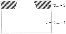
- a positive resist when used, it is generated by exposure. There was a tendency for the diffusion of acid to be inhibited on the side closer to the surface of the n-type semiconductor layer. This tendency is particularly noticeable when a nitride semiconductor is used. Therefore, the resist pattern obtained from the positive resist has a skirting shape (footing shape) as shown in FIG. 1, and the electrode after resist peeling has a burr on the edge portion. There was a problem that was not preferable.
- the present invention is intended to solve the above-mentioned problems of the prior art, and an object of the present invention is to provide a method capable of satisfactorily forming an electrode on an n-type semiconductor layer by a lift-off method.
- the present inventors can form an electrode having a good shape when forming an electrode by MOCVD (metal organic chemical vapor deposition) or the like. It was found that the resist could be peeled off well after electrode formation, and the present invention was completed.
- MOCVD metal organic chemical vapor deposition
- the present invention includes, for example, the following aspects.
- the present invention since a resist having a good reverse taper shape can be formed on the n-type semiconductor layer, an electrode having a good shape can be formed, and the resist can be peeled well after the electrode is formed.
- the present invention has a special effect that a resist having a good reverse taper shape can be formed even on a nitride semiconductor layer that tends to be in a footing shape.
- the method for forming an electrode on an n-type semiconductor layer according to the present invention is performed on the n-type semiconductor layer by a lithography method using a chemically amplified negative resist (hereinafter, also simply referred to as “negative resist” or “resist”).
- a step of forming a resist pattern hereinafter also referred to as “step (1)”
- step (2) a step of forming a metal film between the resist patterns
- step (3) A step of peeling and obtaining an electrode made of the metal film formed on the n-type semiconductor layer.
- the lithography method refers to a pattern formed by selectively irradiating a coating film obtained from a radiation-sensitive composition with radiation (no limitation of wavelength) through a mask as necessary, and then developing. It is a general term for the forming method.
- the n-type semiconductor layer is not particularly limited except that it is made of an n-type semiconductor, but is preferably made of an n-type nitride semiconductor.
- the nitride semiconductor include GaN, AlN, InN, InGaN, AlGaN, Examples include InAlGaN, GaPN, GaNAs, InGaPN, InGaAsN, AlGaPN, AlGaAsN, AlInGaPN, AlInGaAsN, AlGaPAsN, InGaPAsN, and AlInGaPAsN.
- a resist pattern having a good reverse taper shape can be formed even on a nitride semiconductor layer that tends to be a footing shape when a positive resist is used.
- the electrode can be formed.
- the n-type semiconductor layer is an n-type semiconductor layer in a semiconductor light emitting device.
- Examples of the configuration and shape of the electrodes of the semiconductor light emitting device include a normal type in which the upper electrode and the lower electrode face each other and a trench type in which the upper electrode and the lower electrode are in the same direction. Moreover, as a structure and shape of the semiconductor layer of a semiconductor light-emitting device, a double heterojunction type, a quantum well junction type, etc. are mentioned, for example.
- the configuration and shape of the semiconductor light emitting device include, for example, Japanese Patent Application Laid-Open Nos. 2009-170655, 2007-173530, 2007-157778, 2005-294870, and 2004. -29679, JP-A-2004-047662, JP-A-2003-243703, JP-A-2003-88641, JP-A-2002-329885, JP-A-2002-066421, JP-A-2001-274456 JP, 2001-196629, 2001-177147, 2001-068786, 2000-261029, 2000-124502, 10-294531 JP 09-31442 A and JP It includes structural and shape according to the flat 09-237916 JP.
- FIG. 4 shows a cross-sectional view of a current blocking semiconductor light emitting device as a typical example of a semiconductor light emitting device.
- the semiconductor light emitting device of FIG. 4 is provided on a sapphire substrate 100 in the order of a buffer layer 101, a semiconductor layer 110, a current diffusion layer 120, and an upper electrode 131.
- a current blocking layer 140 is provided so as to be located below the upper electrode without being in contact with the upper electrode 131 and to be covered with the current diffusion layer 120.
- the semiconductor layer 110 is a double heterojunction type, and is provided on the buffer layer 101 in the order of an n-type cladding layer 111, an active layer 112, and a p-type cladding layer 113.
- the lower electrode 132 is provided on a part of the n-type cladding layer and is provided in the same direction as the upper electrode 131.
- the buffer layer 101, the semiconductor layer 110, the current diffusion layer 120, and the current blocking layer 140 may be formed by a known method such as a vapor phase epitaxial growth method, a liquid phase epitaxial growth method, a hydride vapor phase growth method, a metal organic vapor phase growth method (MOCVD method). ), Molecular beam epitaxy (MBE), metalorganic molecular beam epitaxy (MOMBE), sputtering, etc., and then, if necessary, can be formed by etching or grinding using a resist as a mask. .
- a known method such as a vapor phase epitaxial growth method, a liquid phase epitaxial growth method, a hydride vapor phase growth method, a metal organic vapor phase growth method (MOCVD method).
- MOCVD method metal organic vapor phase growth method
- MBE Molecular beam epitaxy
- MOMBE metalorganic molecular beam epitaxy
- sputtering etc.
- step (1) of the present invention a resist pattern is formed on the n-type semiconductor layer by a lithography method using a negative resist.
- a negative resist composition is applied directly on the n-type semiconductor layer 11 so as to be in contact with the n-type semiconductor layer 11 and dried.
- a resist film (coating film) 12 is formed by irradiating the resist film 12 with a radiation having a desired pattern if necessary (exposure), and then developing to form a resist pattern 13 To do.
- the resist composition coating method examples include a dipping method, a spray method, a bar coating method, a roll coating method, and a spin coating method.
- the thickness of the coating film can be appropriately controlled by adjusting the solid content concentration and viscosity of the coating means and resist composition.
- the thickness of the coating film can be controlled by changing the rotation speed.
- Examples of radiation used for exposure include ultraviolet rays and electron beams emitted from low-pressure mercury lamps, high-pressure mercury lamps, metal halide lamps, g-line steppers, h-line steppers, i-line steppers, KrF steppers, ArF steppers, EB exposure apparatuses, and the like. And laser beam.
- the exposure amount can be appropriately set depending on the light source used and the film thickness of the coating film. For example, in the case of ultraviolet rays irradiated from a high-pressure mercury lamp, when the coating film thickness is 0.05 to 50 ⁇ m, 100 to It can be about 20,000 J / m 2 .
- PEB heat treatment
- the PEB conditions vary depending on the components and solids concentration of the resist composition used for forming the coating film and the film thickness of the coating film, but are usually 50 to 180 ° C., preferably 60 to 150 ° C., and 1 to 60. It is about a minute.
- a desired pattern can be formed by developing the unexposed portion with an alkaline developer or the like, and dissolving and removing the unexposed portion.
- the development method include a shower development method, a spray development method, an immersion development method, and a paddle development method.
- the development conditions are usually about 20 to 40 ° C. and about 0.5 to 10 minutes.
- the alkaline developer examples include an alkaline aqueous solution in which an alkaline compound such as sodium hydroxide, potassium hydroxide, aqueous ammonia, tetramethylammonium hydroxide, and choline is dissolved in water so as to have a concentration of 1 to 10% by mass. Can be mentioned.
- an appropriate amount of a water-soluble organic solvent such as methanol or ethanol, a surfactant, or the like can be added to the alkaline aqueous solution.
- it is usually washed with water and dried.
- the resist pattern may be further cured by heat treatment.
- Such curing conditions are not particularly limited, but are usually 50 to 600 ° C., more preferably about 1 minute to 10 hours.
- the heat treatment after the development may be performed in two or more steps in order to sufficiently cure the obtained resist pattern or prevent its deformation.
- the resist pattern is cured by heating at a temperature of 100 to 250 ° C. for about 5 minutes to 2 hours in the first stage and heating at a temperature of 250 to 500 ° C. for about 10 minutes to 10 hours in the second stage. Also good.
- the composition containing an alkali-soluble polymer, the compound which has a radically polymerizable unsaturated bond group, and a radiation sensitive radical generator Alkali-soluble polymer A composition containing a compound that undergoes a crosslinking reaction by the action of an acid and a radiation-sensitive acid generator; a polymer that is alkali-soluble and has a radical-polymerizable unsaturated bond group; and a radiation-sensitive radical A composition containing a generator; a composition containing a polymer that is soluble in alkali and has a group that undergoes a crosslinking reaction by the action of an acid, and a radiation-sensitive acid generator, and the like.
- a composition containing is preferred.
- the negative resist further preferably contains a compound (D) that absorbs the wavelength of exposure light used in the lithography method (hereinafter also referred to as “light absorbing compound (D)”).
- the negative resist may contain other components as long as the effects of the present invention are not impaired.
- this invention is not limited to the following aspect.
- the alkali-soluble polymer is a (co) polymer whose solubility in a 2.38% by mass tetraammonium hydroxide aqueous solution (alkaline liquid) of the coating film made of the polymer is 100 kg / sec or more. It is.
- alkali-soluble polymers (A) examples include novolak resins, polyhydroxystyrene and copolymers thereof, phenol-xylylene glycol condensed resins, cresol-xylylene glycol condensed resins, phenol-dicyclopentadiene. Examples thereof include condensed resins and polybenzoxazole precursors. Of these, novolak resins, polyhydroxystyrene and copolymers thereof, and polybenzoxazole precursors are preferred. These resins may be used alone or in combination of two or more.
- the novolak resin is obtained by condensing phenols and aldehydes in the presence of a catalyst.
- the phenols include phenol, o-cresol, m-cresol, p-cresol, o-ethylphenol, m-ethylphenol, p-ethylphenol, o-butylphenol, m-butylphenol, p-butylphenol, 2 , 3-xylenol, 2,4-xylenol, 2,5-xylenol, 2,6-xylenol, 3,4-xylenol, 3,5-xylenol, 2,3,5-trimethylphenol, 3,4,5- Examples include trimethylphenol, catechol, resorcinol, pyrogallol, ⁇ -naphthol, ⁇ -naphthol and the like.
- the aldehydes include formaldehyde, paraformaldehyde, acetaldehy
- novolak resins include phenol / formaldehyde condensed novolak resins, cresol / formaldehyde condensed novolak resins, phenol-naphthol / formaldehyde condensed novolak resins, and the like.
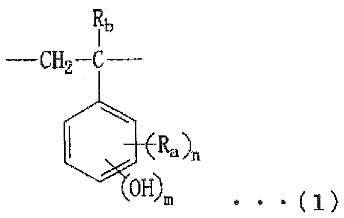
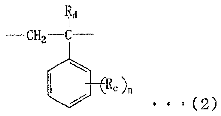
- the polyhydroxystyrene and the copolymer thereof include a copolymer composed of a structural unit (1) represented by the following general formula (1) and a structural unit (2) represented by the following general formula (2).
- Combined (A1) is preferably used.
- the copolymer (A1) is a copolymer of a monomer that can form the structural unit (1) and a monomer that can form the structural unit (2).
- Ra represents an alkyl group having 1 to 4 carbon atoms, an alkoxy group or an allyl group.
- Rb represents a hydrogen atom or a methyl group.
- n is an integer of 0 to 3
- m is an integer of 1 to 3.
- Rc represents an alkyl group having 1 to 4 carbon atoms, an alkoxy group or an allyl group.
- Rd represents a hydrogen atom or a methyl group.
- n is an integer of 0 to 3.
- Examples of the monomer that can form the structural unit (1) include p-hydroxystyrene, m-hydroxystyrene, o-hydroxystyrene, p-isopropenylphenol, m-isopropenylphenol, o-isopropenylphenol, and the like. Can be mentioned. Of these, p-hydroxystyrene and p-isopropenylphenol are preferred.
- the structural unit (1) may be obtained, for example, by polymerizing a monomer having a hydroxyl group protected with a t-butyl group, an acetyl group or the like.
- the obtained polymer or copolymer is converted into a hydroxystyrene-based structural unit by a known method, for example, deprotection under an acid catalyst.
- Examples of the monomer capable of forming the structural unit (2) include styrene, ⁇ -methylstyrene, o-methylstyrene, m-methylstyrene, p-methylstyrene, o-methoxystyrene, m-methoxystyrene, p- Examples include methoxystyrene. Among these, styrene and p-methoxystyrene are preferable, and styrene is more preferable.
- These monomers may be used alone or in combination of two or more.
- the copolymer (A1) is a copolymer of a monomer that can form the structural unit (1) and a monomer that can form the structural unit (2), and is essentially a structural unit (1) and a structural unit. Although it is preferable to consist only of (2), other monomers may be copolymerized.
- Examples of the other monomers include unsaturated carboxylic acids or their anhydrides, esters of the unsaturated carboxylic acids, unsaturated nitriles, unsaturated amides, unsaturated imides, and alicyclic skeletons.
- the amount of structural units formed from other monomers is 100 parts by mass or less with respect to a total of 100 parts by mass of the structural unit (1) and the structural unit (2). Is 50 parts by mass or less, more preferably 25 parts by mass or less.
- the content of the structural unit (1) is 10 to 99 mol%, preferably 20 to 97 mol%, more preferably 30 to 95 mol%, and the structural unit (2)
- the content of is 90 to 1 mol%, preferably 80 to 3 mol%, more preferably 70 to 5 mol% (provided that the total amount of structural units constituting the copolymer (A1) is 100 mol%) And).
- the patterning characteristics may be deteriorated, and physical properties such as thermal shock properties of the cured film may be deteriorated.
- the arrangement of the structural unit (1), the structural unit (2), and the structural unit formed from the other monomers is not particularly limited, and the copolymer (A1) is a random copolymer. Either a polymer or a block copolymer may be used.
- the copolymer (A1) a compound that can form the structural unit (1) or a compound that protects the hydroxyl group thereof, a monomer that can form the structural unit (2), and the above-mentioned other units as necessary.
- the monomer may be polymerized in a solvent in the presence of an initiator.
- the polymerization method is not particularly limited, and may be performed by radical polymerization or anionic polymerization in order to obtain a compound having a desired molecular weight.
- the molecular weight of the polymer (A) is not particularly limited, but the weight average molecular weight (Mw) in terms of polystyrene measured by gel permeation chromatography (GPC) is, for example, 200,000 or less, preferably 2,000 to 100. , 000.
- Mw weight average molecular weight
- GPC gel permeation chromatography
- the acid generator (B) is a component that generates an acid by the exposure. Due to the catalytic action of the acid generated by the acid generator (B), the crosslinking agent (C) can undergo a crosslinking reaction to form a negative pattern.
- the acid generator (B) is not particularly limited as long as it is a compound that generates an acid upon irradiation with radiation or the like.
- onium salt compounds including thiophenium salt compounds
- halogen-containing compounds diazoketone compounds, sulfone compounds , Sulfonic acid compounds, sulfonimide compounds, diazomethane compounds and the like.
- onium salt compounds and halogen-containing compounds are preferable from the viewpoint of resolution and sensitivity of the negative resist, and thiophenium salt compounds and halogen-containing compounds having a triazine structure are more preferable.
- onium salt compound examples include 4,7-di-n-butoxynaphthyltetrahydrothiophenium salt compound, 1- (4-n-butoxynaphthalen-1-yl) tetrahydrothiophenium salt compound, 1- ( Thiophenium salt compounds such as 6-n-butoxynaphthalen-2-yl) tetrahydrothiophenium salt compound, 1- (3,5-dimethyl-4-hydroxyphenyl) tetrahydrothiophenium salt compound; bis (4-t- Iodonium salt compounds such as butylphenyl) iodonium salt compounds and diphenyliodonium salt compounds; triphenylsulfonium salt compounds, 4-tert-butylphenyldiphenylsulfonium salt compounds, 4-cyclohexylphenyldiphenylsulfonium salt compounds, 4-methanesulfonylphenyldi Sulfonium salt compounds such as E sulf
- halogen-containing compound examples include haloalkyl group-containing hydrocarbon compounds and haloalkyl group-containing heterocyclic compounds. Specifically, 1,10-dibromo-n-decane, 1,1-bis (4-chlorophenyl) -2,2,2-trichloroethane, and phenyl-bis (trichloromethyl) -1,3,5- Triazine, 4-methoxyphenyl-bis (trichloromethyl) -1,3,5-triazine, styryl-bis (trichloromethyl) -1,3,5-triazine, naphthyl-bis (trichloromethyl) -1,3,5 -Triazine, 2,4-trichloromethyl (piperonyl) -1,3,5-triazine, 2,4-trichloromethyl- (4-methoxystyryl) -1,3,5-triazine, 2- (1,3- Benzodioxol-5
- the acid generator (B) may be used alone or in combination of two or more.
- the blending amount of the acid generator (B) is preferably 0.1 to 100 parts by mass with respect to 100 parts by mass of the polymer (A) from the viewpoint of ensuring the sensitivity, resolution, pattern shape, etc. of the negative resist. 30 parts by mass, more preferably 0.1 to 20 parts by mass, and still more preferably 0.1 to 15 parts by mass.
- the blending amount is within the above range, the sensitivity and resolution are excellent, the composition is sufficiently cured to improve the heat resistance of the cured film, and has good transparency to radiation, and has a pattern shape. Degradation is less likely to occur.
- the crosslinking agent (C) is a compound that can form a crosslinked structure in the presence of an acid generated from the acid generator (B) by the action of radiation.
- a cross-linking agent (C) is not particularly limited as long as it is a compound exhibiting the above-mentioned action. However, since it can form a pattern that can resist the load on the resist pattern during the formation of the metal film, a methylol group or an alkoxymethylol group can be formed. The compound which has is preferable.
- Examples of the compound having a methylol group or an alkoxymethylol group include melamine compounds, urea compounds, benzoguanamine compounds and glycoluril compounds having a methylol group or an alkoxymethylol group.
- melamine compounds, benzoguanamine compounds, and glycoluril compounds having a methylol group or an alkoxymethylol group are preferred, and in particular, because a pattern with excellent heat resistance that can counter the thermal history applied during metal film formation can be formed.
- a melamine compound having a methylol group or an alkoxymethylol group is preferred.
- Examples of the melamine compound having a methylol group or an alkoxymethylol group include methoxymethylated melamine, ethoxymethylated melamine, n-propoxymethylated melamine, n-butoxymethylated melamine, and more specifically, Examples include hexamethoxymethyl melamine and hexabutoxymethyl melamine.
- benzoguanamine compounds having a methylol group or an alkoxymethylol group include, for example, tetramethylol benzoguanamine, alkylated methylol benzoguanamine (the number of alkylation is 1 to 4.
- Alkyl is an alkyl group having 1 to 6 carbon atoms. Etc.).
- glycoluril-based compound having a methylol group or an alkoxymethylol group examples include methoxymethylated glycoluril, ethoxymethylated glycoluril, n-propoxymethylated glycoluril, n-butoxymethylated glycoluril, and the like. More specifically, tetramethoxymethyl glycoluril, tetrabutoxymethyl glycoluril and the like can be mentioned.
- the crosslinking agent (C) may be used alone or in combination of two or more.
- the amount of the crosslinking agent (C) is preferably 3 to 60 parts by weight, more preferably 3 to 40 parts by weight, and still more preferably 5 to 30 parts by weight with respect to 100 parts by weight of the polymer (A). Part.
- the amount of the crosslinking agent is too small, it is difficult to sufficiently advance the crosslinking reaction, and as a resist, the residual film ratio is decreased, pattern swelling, meandering, etc. are likely to occur.
- the amount is too large, the resolution as a resist tends to be lowered.
- the light-absorbing compound (D) is a compound that absorbs the wavelength of exposure light used in the lithography method, and the negative resist contains the light-absorbing compound (D), so that the light is n-type semiconductor substrate. Therefore, a larger resist pattern having a reverse taper shape can be formed.
- Examples of the light absorbing compound (D) include curcumin and 3-methyl-5-hydroxy-1- (phenyl) -4- (tolylazo) -pyrazole.
- the light absorbing compound (D) may be used alone or in combination of two or more.
- the amount of the light absorbing compound (D) is preferably 0.01 to 20 parts by weight, more preferably 0.05 to 10 parts by weight, and still more preferably 100 parts by weight of the polymer (A). Is 0.1 to 5 parts by mass. When the blending amount is within the above range, the reverse taper shape of the resist pattern can be formed satisfactorily, and the resist pattern can be formed without reducing the sensitivity.
- ⁇ Other ingredients examples include solvents, surfactants, solubility aids, crosslinked polymer particles, adhesion aids, leveling agents, antifoaming agents, crosslinking accelerators, acid diffusion control agents, sensitizers, and sensitizers.
- An auxiliary agent etc. are mentioned.
- the solvent is added to improve the handleability of the resist composition and to adjust the viscosity and storage stability.
- a solvent is not particularly limited. Ethylene glycol monoalkyl ether acetates such as ethylene glycol monomethyl ether acetate and ethylene glycol monoethyl ether acetate; Propylene glycol monoalkyl ethers such as propylene glycol monomethyl ether, propylene glycol monoethyl ether, propylene glycol monopropyl ether, propylene glycol monobutyl ether; Propylene glycol dialkyl ethers such as propylene glycol dimethyl ether, propylene glycol diethyl ether, propylene glycol dipropyl ether, propylene glycol dibutyl ether; Propylene glycol monoalkyl ether acetates such as propylene glycol monomethyl ether acetate, propylene glycol monoethyl ether acetate, propylene glycol monopropy
- the above solvents may be used alone or in combination of two or more.
- the amount of the solvent is not particularly limited as long as the composition can be made uniform, but is preferably 10 to 500 parts by weight, more preferably 100 to 300 parts by weight with respect to 100 parts by weight of the polymer. More preferably, it is 150 to 250 parts by mass.
- the above surfactant is added to improve the flattening of the coating film, the flattening of the outer periphery of the substrate, the striation, and the like.
- surfactants include silicon surfactants, fluorine surfactants, and acrylic surfactants.
- F-top EF301, EF303, EF352 manufactured by Tochem Products
- MegaFuck F171, F172, F173 manufactured by Dainippon Ink and Chemicals
- Florard FC430, FC431 manufactured by Sumitomo 3M
- Surflon Fluorosurfactants such as S-381, S-382, SC101, SC102, SC103, SC104, SC105, SC106 (made by Asahi Glass Co., Ltd.), Footgent 250, 251, 222F, FTX-218 (made by Neos), etc.
- S-381, S-382, SC101, SC102, SC103, SC104, SC105, SC106 made by Asahi Glass Co., Ltd.
- Footgent 250, 251, 222F, FTX-218 made by Neos
- the above surfactants may be used alone or in combination of two or more.
- the surfactant is preferably 0.01 to 1 part by mass, more preferably 0.01 to 0.5 part by mass with respect to 100 parts by mass of the polymer (A).
- solubility aid examples include 4,4′-dihydroxydiphenylmethane, 4,4′-dihydroxydiphenyl ether, tris (4-hydroxyphenyl) methane, and 1,1-bis (4-hydroxyphenyl) -1-phenyl.
- Ethane tris (4-hydroxyphenyl) ethane, 1,3-bis [1- (4-hydroxyphenyl) -1-methylethyl] benzene, 1,4-bis [1- (4-hydroxyphenyl) -1- Methylethyl] benzene, 4,6-bis [1- (4-hydroxyphenyl) -1-methylethyl] -1,3-dihydroxybenzene, 1,1-bis (4-hydroxyphenyl) -1- [4- ⁇ 1- (4-hydroxyphenyl) -1-methylethyl ⁇ phenyl] ethane, 1,1,2,2-tetra (4-hydroxyphenyl) ethane, 4 , 4 '-[1- ⁇ 4- [2- (4-hydroxyphenyl) -2-propyl] phenyl ⁇ ethylidene] bisphenol, 4,4'-[1- ⁇ 4- [1- (4-hydroxyphenyl)] -1-methylethyl] bis
- solubility aids may be used alone or in combination of two or more. Further, the blending amount of the solubility aid is preferably 1 to 50 parts by mass, more preferably 2 to 30 parts by mass, and further preferably 3 to 20 parts by mass with respect to 100 parts by mass of the polymer (A). It is.
- acid diffusion control agent examples include acid diffusion control agents described in JP-A-2008-192774, for example, mono (cyclo) alkylamines such as n-hexylamine, n-heptylamine, n-octylamine, n-nonylamine, n-decylamine, cyclohexylamine; Di-n-butylamine, di-n-pentylamine, di-n-hexylamine, di-n-heptylamine, di-n-octylamine, di-n-nonylamine, di-n-decylamine, cyclohexylmethylamine, Di (cyclo) alkylamines such as dicyclohexylamine; Triethylamine, tri-n-propylamine, tri-n-butylamine, tri-n-pentylamine, tri-n-hexylamine, tri-n-heptylamine, tri-n-o
- an amine having a carbamate structure is preferable because a good reverse taper shape can be easily obtained.
- the above acid diffusion controller may be used alone or in combination of two or more.
- the amount of the acid diffusion control agent is preferably 0.001 to 10 parts by mass, more preferably 0.005 to 5 parts by mass, and still more preferably 0 to 100 parts by mass of the polymer (A). 0.01 to 1 part by mass.
- Step (2) In the step (2) of the present invention, as shown in FIG. 3C, a metal film 14 is formed between the resist patterns 13 formed in the step (1).
- Examples of the method for forming the metal film include a vacuum deposition method and a sputtering method.
- the metal material which comprises an electrode is not specifically limited, For example, gold
- step (3) of the present invention as shown in FIG. 3 (d), after forming the metal film 14 in the step (2), the resist pattern 13 is peeled off to form on the n-type semiconductor layer 1.
- the electrode 14 made of the metal film is obtained.
- the resist pattern peeling method is not particularly limited, and examples thereof include a method of immersing the substrate in a peeling solution at about 20 to 80 ° C. for about 1 to 30 minutes.
- the stripper include dimethyl sulfoxide, N, N-dimethylformamide, N-methylpyrrolidone, ⁇ -butyrolactone, methanolamine, ethanolamine, propanolamine, butanolamine, and mixed solvents thereof.
- the resist pattern can be favorably peeled without impairing the electrode shape.
- the electrode having a good shape can be formed on the n-type semiconductor substrate by the above-described method for forming an electrode on the n-type semiconductor layer of the present invention.
- weight average molecular weight in the following is a weight average molecular weight in terms of standard polystyrene measured by GPC under the following conditions.
- Component A1 A copolymer containing 80 mol% of p-hydroxystyrene units and 20 mol% of styrene units (weight average molecular weight: 10,000).
- a novolak resin (weight average molecular weight: 7,000) obtained by polycondensation of mixed phenols of component A3: m-cresol: p-cresol 50: 50 (molar ratio) with formalin.
- Component A4 A copolymer (weight average molecular weight: 10,000) containing 80 mol% of units composed of p-hydroxystyrene, 10 mol% of units of styrene, and 10 mol% of units composed of hydroxybutyl acrylate.
- RA1 component a copolymer containing 50% by mass of 1-ethylcyclohexyl methacrylate structural unit and 50% by mass of 2-ethoxyethyl acrylate structural unit (weight average molecular weight: 350,000).
- B1 2- [2- (5-methylfuran-2-yl) ethenyl] -4,6-bis- (trichloromethyl) -1,3,5-triazine.
- B2 component 2,4-trichloromethyl (piperonyl) -1,3,5-triazine.
- B3 component 2,4-trichloromethyl- (4-methoxystyryl) -1,3,5-triazine.
- B4 component 1- (4,7-dibutoxy-1-naphthalenyl) tetrahydrothiophenium trifluoromethanesulfonate.
- B5 component a compound represented by the following formula.
- Component B6 4,4 ′-[1- [4- [1- [4-hydroxyphenyl] -1-methylethyl] phenyl] ethylidene] bisphenol (1.0 mol) and 1,2-naphthoquinonediazide-5 A condensate of sulfonic acid chloride (2.0 mol).
- ⁇ C component; cross-linking agent> C1 component: hexamethoxymethyl melamine.
- Component C2 tetramethoxymethyl glycoluril.
- C3 component Tetramethylol benzoguanamine.
- D1 component curcumin.
- Component D2 3-methyl-5-hydroxy-1- (phenyl) -4- (tolylazo) -pyrazole.
- E1 component Fluorosurfactant (trade name “Factent 251”, manufactured by Neos).
- F1 component 4,4 ′-[1- ⁇ 4 [1- (4-hydroxyphenyl) -1-methylethyl] phenyl ⁇ ethylidene] bisphenol.
- G component methyl 3-methoxypropionate.
- G2 component propylene glycol monomethyl ether acetate.
- H1 component N, N-dicyclohexylcarbamic acid-1,1-dimethylethyl ester.
- H2 component Nt-butoxycarbonylpyrrolidine.
- H3 component Nt monobutoxycarbonyl-2 monophenylbenzimidazole.
- the obtained pattern has a good reverse taper shape with no footing.
- Defect The obtained pattern has at least one shape of footing and forward taper shape.
- n-type GaN substrate surface state having protrusions with a height of 1.2 ⁇ m to 0.4 ⁇ m.
- the film thickness of the coating film in the case of an n-type GaN substrate indicates the thickness from a protrusion having a height of 1.2 ⁇ m.
- ITO substrate a substantially flat surface state having a tin-doped indium oxide film on the surface.
Landscapes
- Physics & Mathematics (AREA)
- General Physics & Mathematics (AREA)
- Spectroscopy & Molecular Physics (AREA)
- Chemical & Material Sciences (AREA)
- Engineering & Computer Science (AREA)
- Ceramic Engineering (AREA)
- Condensed Matter Physics & Semiconductors (AREA)
- Electromagnetism (AREA)
- Optics & Photonics (AREA)
- Electrodes Of Semiconductors (AREA)
- Materials For Photolithography (AREA)
- Internal Circuitry In Semiconductor Integrated Circuit Devices (AREA)
Abstract
Description
上記n型半導体層は、n型半導体からなること以外は特に限定されないが、n型窒化物半導体からなることが好ましく、該窒化物半導体としては、例えば、GaN、AlN、InN、InGaN、AlGaN、InAlGaN、GaPN、GaNAs、InGaPN、InGaAsN、AlGaPN、AlGaAsN、AlInGaPN、AlInGaAsN、AlGaPAsN、InGaPAsN、AlInGaPAsNなどが挙げられる。本発明によれば、ポジ型レジストを用いた場合にフッティング形状となる傾向が強い窒化物半導体層上にも良好な逆テーパー形状のレジストパターンを形成することができ、その結果、良好な形状の電極を形成することができる。また、上記n型半導体層が半導体発光素子におけるn型半導体層であることが、本発明の好ましい態様である。
半導体発光素子の電極の構成や形状としては、例えば、上部電極と下部電極が対向するような通常型、および、上部電極と下部電極が同じ向きにあるトレンチ型などが挙げられる。また、半導体発光素子の半導体層の構成や形状としては、例えば、ダブルへテロ接合型および量子井戸接合型などが挙げられる。
本発明の工程(1)では、ネガ型レジストを用いたリソグラフィー法によりn型半導体層上にレジストパターンを形成する。
上記ネガ型レジストとしては、特に限定されないが、例えば、アルカリ可溶性重合体と、ラジカル重合性の不飽和結合基を有する化合物と、感放射線性ラジカル発生剤とを含有する組成物;アルカリ可溶性重合体と、酸の作用により架橋反応を起こす化合物と、感放射線性酸発生剤とを含有する組成物;アルカリ可溶性であり、かつラジカル重合性の不飽和結合基を有する重合体と、感放射線性ラジカル発生剤とを含有する組成物;アルカリ可溶性であり、かつ酸の作用により架橋反応起こす基を有する重合体と、感放射線性酸発生剤とを含有する組成物などが挙げられる。これらの中では、アルカリ可溶性重合体(A)、感放射線性酸発生剤(B)(以下「酸発生剤(B)」ともいう。)および酸の作用により架橋反応を起こす架橋剤(C)を含有する組成物が好ましい。また、上記ネガ型レジストは、上記リソグラフィー法に用いる露光光の波長を光吸収する化合物(D)(以下「光吸収化合物(D)」ともいう。)をさらに含有することが、より好ましい。さらに、上記ネガ型レジストは、本発明の効果を損なわない範囲で、他の成分を含有してもよい。以下、本発明で用いられるネガ型レジストとして好ましい態様を説明するが、本発明は下記態様に限定されるものではない。
上記アルカリ可溶性重合体とは、該重合体からなる塗膜の、2.38質量%のテトラアンモニウムハイドロオキサイド水溶液(アルカリ性の液)に対する溶解度が、100Å/秒以上となる(共)重合体のことである。
上記酸発生剤(B)は、上記露光により酸を発生する成分である。酸発生剤(B)により発生した酸の触媒作用により、架橋剤(C)が架橋反応を起こし、ネガ型のパターンを形成することができる。
上記架橋剤(C)は、放射線の作用により上記酸発生剤(B)より発生する酸の存在下で、架橋構造を形成し得る化合物である。このような架橋剤(C)としては、前記作用を示す化合物であれば特に限定されないが、金属膜形成時におけるレジストパターンへの負荷に対抗できるパターンを形成できることから、メチロール基またはアルコキシメチロール基を有する化合物が好ましい。
上記光吸収化合物(D)は、上記リソグラフィー法に用いる露光光の波長を光吸収する化合物であり、上記ネガ型レジストが該光吸収化合物(D)を含有することにより、光がn型半導体基板まで透過できなくなるため、より大きな逆テーパー形状のレジストパターンを形成することができる。
上記他の成分としては、例えば、溶剤、界面活性剤、溶解性補助剤、架橋ポリマー粒子、密着助剤、レベリング剤、消泡剤、架橋促進剤、酸拡散制御剤、増感剤、増感助剤などが挙げられる。
エチレングリコールモノメチルエーテルアセテート、エチレングリコールモノエチルエーテルアセテート等のエチレングリコールモノアルキルエーテルアセテート類;
プロピレングリコールモノメチルエーテル、プロピレングリコールモノエチルエーテル、プロピレングリコールモノプロピルエーテル、プロピレングリコールモノブチルエーテル等のプロピレングリコールモノアルキルエーテル類;
プロピレングリコールジメチルエーテル、プロピレングリコールジエチルエーテル、プロピレングリコールジプロピルエーテル、プロピレングリコールジブチルエーテル等のプロピレングリコールジアルキルエーテル類;
プロピレングリコールモノメチルエーテルアセテート、プロピレングリコールモノエチルエーテルアセテート、プロピレングリコールモノプロピルエーテルアセテート、プロピレングリコールモノブチルエーテルアセテート等のプロピレングリコールモノアルキルエーテルアセテート類;
エチルセロソルブ、ブチルセロソルブ等のセロソルブ類、ブチルカルビトール等のカルビトール類;
乳酸メチル、乳酸エチル、乳酸n-プロピル、乳酸イソプロピル等の乳酸エステル類;
酢酸エチル、酢酸n-プロピル、酢酸イソプロピル、酢酸n-ブチル、酢酸イソブチル、酢酸n-アミル、酢酸イソアミル、プロピオン酸イソプロピル、プロピオン酸n-ブチル、プロピオン酸イソブチル等の脂肪族カルボン酸エステル類;
3-メトキシプロピオン酸メチル、3-メトキシプロピオン酸エチル、3-エトキシプロピオン酸メチル、3-エトキシプロピオン酸エチル、ピルビン酸メチル、ピルビン酸エチル等の他のエステル類;
トルエン、キシレン等の芳香族炭化水素類;
2-ヘプタノン、3-ヘプタノン、4-ヘプタノン、シクロヘキサノン等のケトン類;
N-ジメチルホルムアミド、N-メチルアセトアミド、N,N-ジメチルアセトアミド、N-メチルピロリドン等のアミド類;
γ-ブチロラクトン等のラクトン類
などの有機溶媒が挙げられる。
n-ヘキシルアミン、n-ヘプチルアミン、n-オクチルアミン、n-ノニルアミン、n-デシルアミン、シクロヘキシルアミン等のモノ(シクロ)アルキルアミン類;
ジ-n-ブチルアミン、ジ-n-ペンチルアミン、ジ-n-ヘキシルアミン、ジ-n-ヘプチルアミン、ジ-n-オクチルアミン、ジ-n-ノニルアミン、ジ-n-デシルアミン、シクロヘキシルメチルアミン、ジシクロヘキシルアミン等のジ(シクロ)アルキルアミン類;
トリエチルアミン、トリ-n-プロピルアミン、トリ-n-ブチルアミン、トリ-n-ペンチルアミン、トリ-n-ヘキシルアミン、トリ-n-ヘプチルアミン、トリ-n-オクチルアミン、トリ-n-ノニルアミン、トリ-n-デシルアミン、シクロヘキシルジメチルアミン、メチルジシクロヘキシルアミン、トリシクロヘキシルアミン等のトリ(シクロ)アルキルアミン類;
尿素、メチルウレア、1,1-ジメチルウレア、1,3-ジメチルウレア、1,1,3,3-テトラメチルウレア、1,3-ジフェニルウレア、トリ-n-ブチルチオウレア等のウレア化合物;
イミダゾール、4-メチルイミダゾール、4-メチル-2-フェニルイミダゾール、ベンズイミダゾール、2-フェニルベンズイミダゾール、1-ベンジル-2-メチルイミダゾール、1-ベンジル-2-メチル-1H-イミダゾール等のイミダゾール類;
ピリジン、2-メチルピリジン、4-メチルピリジン、2-エチルピリジン、4-エチルピリジン、2-フェニルピリジン、4-フェニルピリジン、2-メチル-4-フェニルピリジン、ニコチン、ニコチン酸、ニコチン酸アミド、キノリン、4-ヒドロキシキノリン、8-オキシキノリン、アクリジン、2,2’:6’,2’’-ターピリジン等のピリジン類;
ピペラジン、1-(2-ヒドロキシエチル)ピペラジン等のピペラジン類;
N,N-ジシクロヘキシルカルバミン酸-1,1-ジメチルエチルエステル、N-t-ブトキシカルボニル-1-アダマンチルアミン、N-t-ブトキシカルボニル-2-アダマンチルアミン、(S)-(-)-1-(t-ブトキシカルボニル)-2-ピロリジンメタノール、(R)-(+)-1-(t-ブトキシカルボニル)-2-ピロリジンメタノール、N-t-ブトキシカルボニルピロリジン、N-t-ブトキシカルボニル-4-ヒドロキシピペリジン、N-t-ブトキシカルボニル-2-フェニルベンズイミダゾール、N-t-アミロキシカルボニルジシクロヘキシルアミン、N-t-アミロキシカルボニル-1-アダマンチルアミン、N-t-アミロキシカルボニル-2-アダマンチルアミン、(S)-(-)-1-(t-アミロキシカルボニル)-2-ピロリジンメタノール、(R)-(+)-1-(t-アミロキシカルボニル)-2-ピロリジンメタノール、N-t-アミロキシカルボニルピロリジン、N-t-アミロキシカルボニル-4-ヒドロキシピペリジン、N-t-アミロキシカルボニル-2-フェニルベンズイミダゾール等のカルバミン酸エステル構造を有するアミン;
ピラジン、ピラゾール、ピリダジン、キノザリン、プリン、ピロリジン、ピペリジン、ピペリジンエタノール、3-ピペリジノ-1,2-プロパンジオール、モルホリン、4-メチルモルホリン、1-(4-モルホリニル)エタノール、4-アセチルモルホリン、3-(N-モルホリノ)-1,2-プロパンジオール、1,4-ジメチルピペラジン、1,4-ジアザビシクロ[2.2.2]オクタン、4,4’-ジアミノジフェニルエーテル、4,4’-ジアミノベンゾフェノン、4,4’-ジアミノジフェニルアミン、2,2-ビス(4-アミノフェニル)プロパン、2-(3-アミノフェニル)-2-(4-アミノフェニル)プロパン、2-(4-アミノフェニル)-2-(3-ヒドロキシフェニル)プロパン、2-(4-アミノフェニル)-2-(4-ヒドロキシフェニル)プロパン、1,4-ビス〔1-(4-アミノフェニル)-1-メチルエチル〕ベンゼン、1,3-ビス〔1-(4-アミノフェニル)-1-メチルエチル〕ベンゼン、ビス(2-ジメチルアミノエチル)エーテル、ビス(2-ジエチルアミノエチル)エーテル、1-(2-ヒドロキシエチル)-2-イミダゾリジノン、2-キノキサリノール、N,N,N’,N’-テトラキス(2-ヒドロキシプロピル)エチレンジアミン、N,N,N’,N’’,N’’-ペンタメチルジエチレントリアミン等のその他アミン類などが挙げられる。
本発明の工程(2)では、図3(c)に示すように、上記工程(1)で形成されたレジストパターン13間に金属膜14を形成する。このようにしてレジストパターン間に形成された金属膜が電極となる。金属膜の形成方法としては、例えば、真空蒸着法、スパッタリング法などが挙げられる。電極を構成する金属材料は特に限定されないが、例えば、金、銀、銅、白金、パラジウム、ニッケル、アルミニウムや、これらの2種以上の合金が挙げられる。
本発明の工程(3)では、図3(d)に示すように、上記工程(2)における金属膜14の形成後、レジストパターン13を剥離することにより、前記n型半導体層1上に形成された前記金属膜からなる電極14を得る。レジストパターンの剥離方法としては、特に限定されないが、例えば、20~80℃程度の剥離液に基板を1~30分間程度浸漬する方法などが挙げられる。前記剥離液としては、例えば、ジメチルスルホキシド、N,N-ジメチルホルムアミド、N-メチルピロリドン、γ-ブチロラクトン、メタノールアミン、エタノールアミン、プロパノールアミン、ブタノールアミンおよびそれらの混合溶剤などが挙げられる。本発明では、逆テーパー形状のレジストパターンを形成しているため、電極の形状を損なうことなく、レジストパターンを良好に剥離することができる。
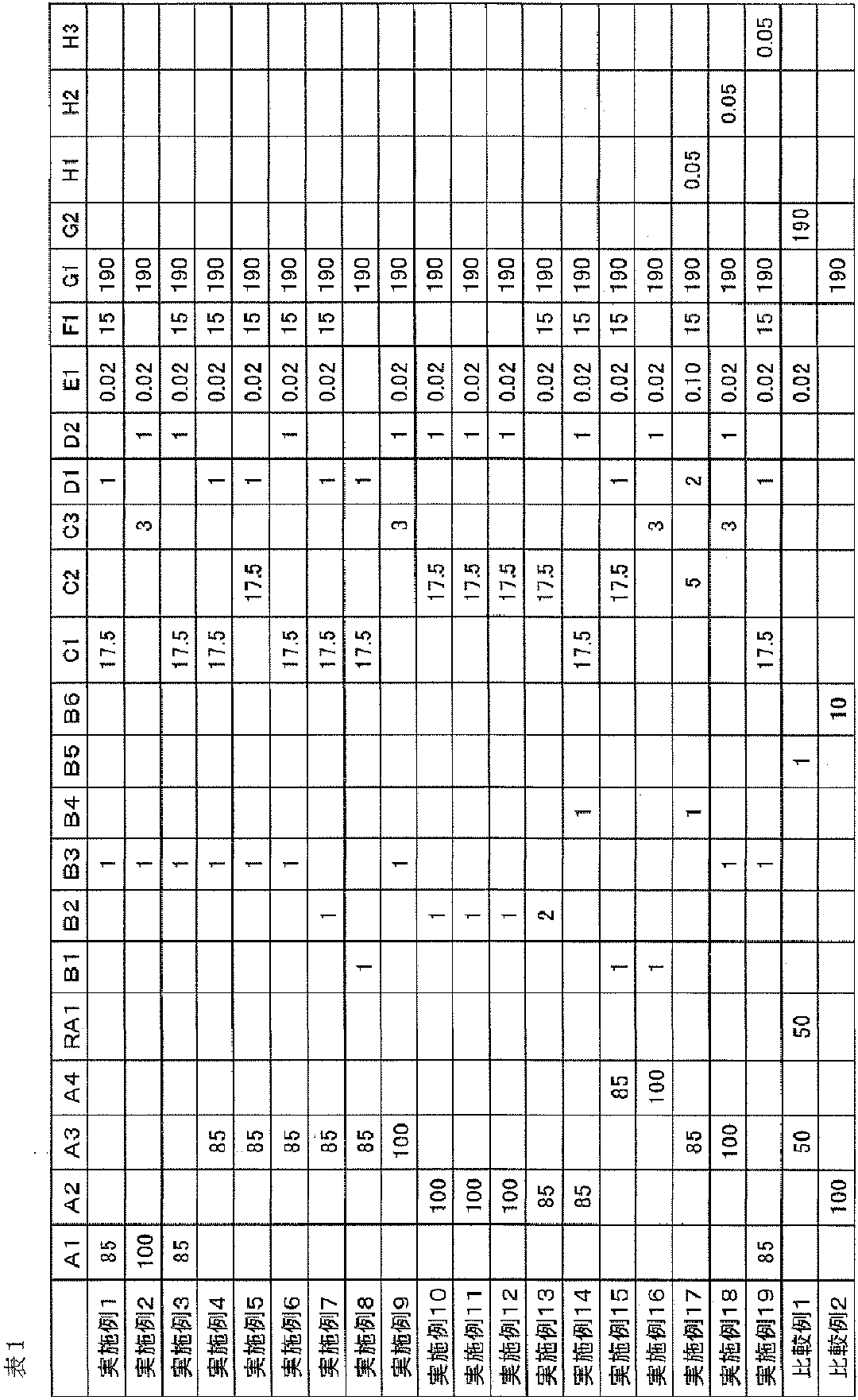
〔1〕レジスト組成物の調製
下記表1に示す量で各成分を配合して溶解することにより、レジスト組成物を調製した。なお、表1における成分量の単位は質量部である。
装置:東ソー(株)製「HLC-8120C」
カラム:東ソー(株)製「TSK-gel MultiporeHXL-M」
溶離液:テトラヒドロフラン、流量0.5mL/min、負荷量5.0%、100μL
カラム温度:40℃。
A1成分:p-ヒドロキシスチレンからなる単位80モル%およびスチレンからなる単位20モル%を含む共重合体(重量平均分子量:10,000)。
A2成分:m-クレゾール:3,5-キシレノール=70:30(モル比)の混合フェノール類をホルマリンと重縮合して得られたノボラック樹脂(重量平均分子量:8,000)。
A3成分:m-クレゾール:p-クレゾール=50:50(モル比)の混合フェノール類をホルマリンと重縮合して得られたノボラック樹脂(重量平均分子量:7,000)。
A4成分:p-ヒドロキシスチレンからなる単位80モル%、スチレンからなる単位10モル%およびヒドロキシブチルアクリレートからなる単位10モル%を含む共重合体(重量平均分子量:10,000)。
RA1成分:1-エチルシクロヘキシルメタクリレート構成単位50質量%および2-エトキシエチルアクリレート構成単位50質量%を含む共重合体(重量平均分子量:350,000)。
B1成分:2-[2-(5-メチルフラン-2-イル)エテニル]-4,6-ビス-(トリクロロメチル)-1,3,5-トリアジン。
B2成分:2,4-トリクロロメチル(ピペロニル)-1,3,5-トリアジン。
B3成分:2,4-トリクロロメチル-(4-メトキシスチリル)-1,3,5-トリアジン。
B4成分:1-(4,7-ジブトキシ-1-ナフタレニル)テトラヒドロチオフェニウムトリフルオロメタンスルホナート。
B5成分:下記式で表される化合物。

C1成分:ヘキサメトキシメチルメラミン。
C2成分:テトラメトキシメチルグリコールウリル。
C3成分:テトラメチロールベンゾグアナミン。
D1成分:クルクミン。
D2成分:3-メチル-5-ヒドロキシ-1-(フェニル)-4-(トリルアゾ)-ピラゾール。
E1成分:フッ素系界面活性剤(商品名「フタージェント251」、ネオス社製)。
F1成分:4,4’-〔1-{4[1-(4-ヒドロキシフェニル)-1-メチルエチル]フェニル}エチリデン〕ビスフェノール。
G1成分:3-メトキシプロピオン酸メチル。
G2成分:プロピレングリコールモノメチルエーテルアセテート。
H1成分:N,N-ジシクロヘキシルカルバミン酸-1,1-ジメチルエチルエステル。
H2成分:N-t一ブトキシカルボニルピロリジン。
H3成分:N-t一ブトキシカルボニルー2一フェニルベンズイミダゾール。
〔2-1〕パターン形状
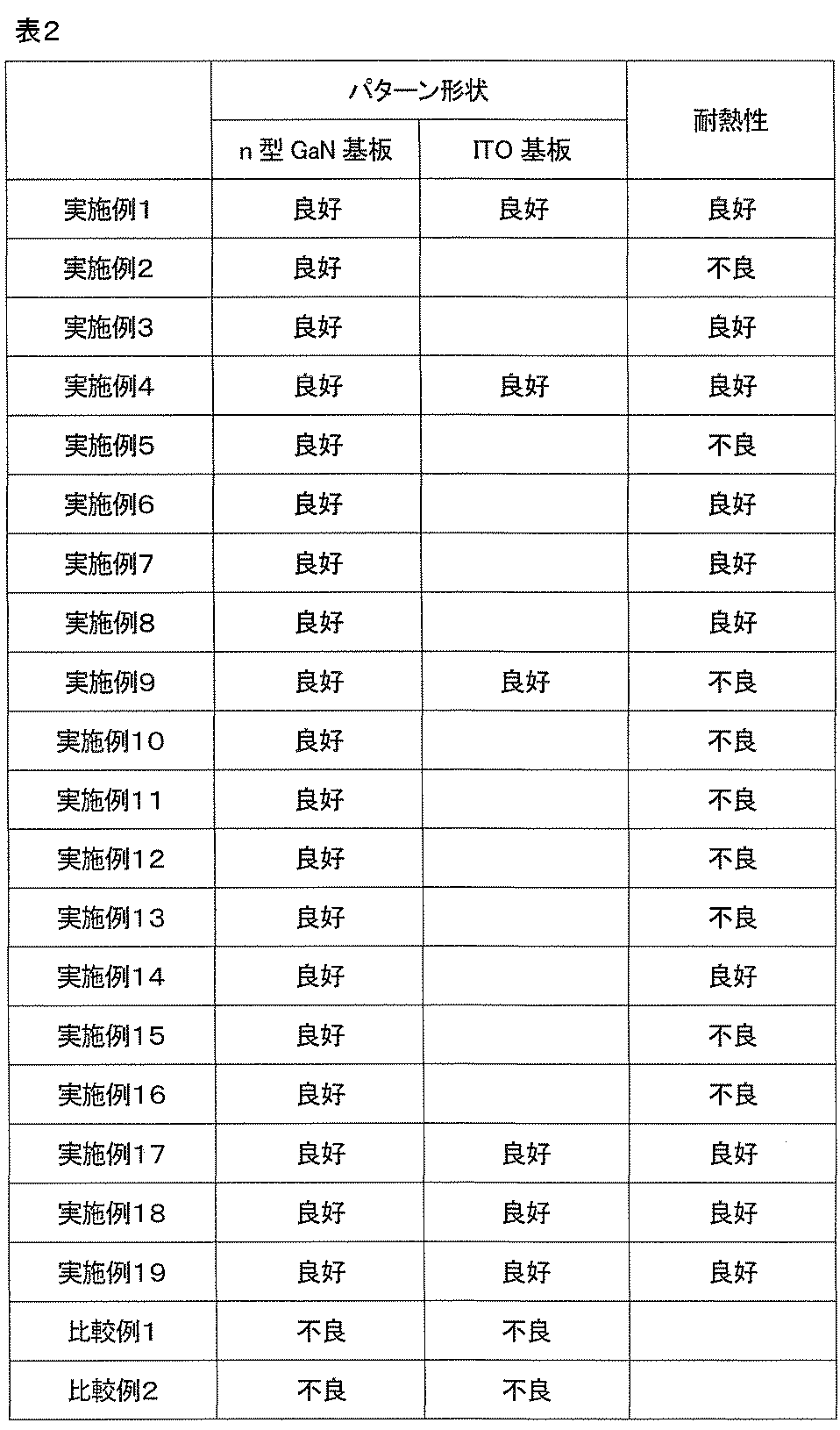
n型GaN基板上もしくはITO基板上に、〔1〕で調製した各レジスト組成物をスピンコートし、その後、ホットプレートを用いて95℃で90秒間加熱し、厚さ5μmの塗膜を作製した。次いで、アライナー(Karl Suss社製、型式「MA-200e」)を使用し、高圧水銀灯から照射される紫外線(波長365nm)を、ホールパターンマスクを介して塗膜に露光した。その後、露光処理した基板を、ホットプレートを用いて95℃で2分間加熱(PEB)した後、2.38質量%濃度のテトラメチルアンモニウムハイドロキサイド水溶液中に、23℃で60秒間浸漬処理することにより現像した。得られたパターンを電子顕微鏡にて観察し、下記基準にて評価した。評価結果を表2に示す。
良好:得られたパターンが、フッティングがない、良好な逆テーパー形状である。
不良:得られたパターンが、フッティング及び順テーパー形状の少なくとも1つ以上の形状である。
n型GaN基板:高さ1.2μm~0.4μmの突起を有する表面状態。n型GaN基板の場合の塗膜の膜厚は、高さ1.2μmの突起からの厚さを示す。
ITO基板:表面にスズドープ酸化インジウム膜を有する略平坦な表面状態である。
前記〔2-1〕で得られたパターンを、ホットプレートを用いて100℃10分間加熱し、加熱後のパターンを電子顕微鏡にて観察し、下記基準にて評価した。評価結果を表2に示す。
良好:加熱前後でパターン形状はほとんど変化なし。
不良:加熱前後でパターン形状が変化し、パターンが埋まるなど、良好な逆テーパーパターンとならない。
実施例1で作製した、レジストパターンが形成された基板上に、スパッタ装置(サンユー電子社製「クイックオートコーターSC-704AT」)を用いて、金からなる金属膜を形成した。次いで、N-メチルピロリドンを用いて23℃でレジストパターンを剥離することにより、基板上に良好な形状の電極を形成することができた。
2 ポジ型レジストパターン
3 ネガ型レジストパターン
11 n型半導体層
12 レジスト膜
13 レジストパターン
14 金属膜(電極)
100 サファイヤ基板
101 バッファ層
110 半導体層
111 n型クラッド層
112 活性層
113 p型クラッド層
120 電流拡散層
131 上部電極
132 下部電極
140 電流阻止層
Claims (10)
- 化学増幅型ネガ型レジストを用いたリソグラフィー法によりn型半導体層上にレジストパターンを形成する工程と、
前記レジストパターン間に金属膜を形成する工程と、
前記レジストパターンを剥離し、前記n型半導体層上に形成された前記金属膜からなる電極を得る工程と
を含むことを特徴とするn型半導体層上の電極の形成方法。 - 前記n型半導体層が、半導体発光素子におけるn型半導体層であることを特徴とする請求項1に記載のn型半導体層上の電極の形成方法。
- 前記化学増幅型ネガ型レジストが、前記リソグラフィー法に用いる露光光の波長を光吸収する化合物を含有することを特徴とする請求項1または2に記載のn型半導体層上の電極の形成方法。
- 前記化学増幅型ネガ型レジストが、酸の作用により架橋反応を起こす架橋剤として、メチロール基又はアルコキシメチロール基を有する化合物を含有することを特徴とする請求項1~3のいずれかに記載のn型半導体層上の電極の形成方法。
- 前記メチロール基またはアルコキシメチロール基を有する化合物がメラミン化合物であることを特徴とする請求項4に記載のn型半導体層上の電極の形成方法。
- 前記n型半導体層がn型窒化物半導体からなることを特徴とする請求項1~5のいずれかに記載のn型半導体層上の電極の形成方法。
- 請求項1~6のいずれかに記載のn型半導体層上の電極の形成方法により得られたことを特徴とするn型半導体層上の電極。
- 請求項1~6のいずれかに記載のn型半導体層上の電極の形成方法に用いられる化学増幅型ネガ型レジスト。
- アルカリ可溶性重合体(A)、感放射線性酸発生剤(B)および酸の作用により架橋反応を起こす架橋剤(C)を含有することを特徴とする請求項8に記載の化学増幅型ネガ型レジスト。
- 前記n型半導体層上の電極の形成方法におけるリソグラフィー法に用いる露光光の波長を光吸収する化合物(D)をさらに含有することを特徴とする請求項9に記載の化学増幅型ネガ型レジスト。
Priority Applications (2)
| Application Number | Priority Date | Filing Date | Title |
|---|---|---|---|
| KR1020127010194A KR20120127386A (ko) | 2010-02-19 | 2010-12-28 | n형 반도체층 상의 전극의 형성 방법, n형 반도체층 상의 전극, 및 화학 증폭형 네거티브형 레지스트 |
| JP2012500477A JPWO2011102064A1 (ja) | 2010-02-19 | 2010-12-28 | n型半導体層上の電極の形成方法 |
Applications Claiming Priority (2)
| Application Number | Priority Date | Filing Date | Title |
|---|---|---|---|
| JP2010034545 | 2010-02-19 | ||
| JP2010-034545 | 2010-02-19 |
Publications (1)
| Publication Number | Publication Date |
|---|---|
| WO2011102064A1 true WO2011102064A1 (ja) | 2011-08-25 |
Family
ID=44482673
Family Applications (1)
| Application Number | Title | Priority Date | Filing Date |
|---|---|---|---|
| PCT/JP2010/073768 Ceased WO2011102064A1 (ja) | 2010-02-19 | 2010-12-28 | n型半導体層上の電極の形成方法 |
Country Status (4)
| Country | Link |
|---|---|
| JP (1) | JPWO2011102064A1 (ja) |
| KR (1) | KR20120127386A (ja) |
| TW (1) | TW201130020A (ja) |
| WO (1) | WO2011102064A1 (ja) |
Cited By (9)
| Publication number | Priority date | Publication date | Assignee | Title |
|---|---|---|---|---|
| JP2016017998A (ja) * | 2014-07-04 | 2016-02-01 | 豊田合成株式会社 | 半導体装置の製造方法、レジストパターンの形成方法 |
| JP2017106955A (ja) * | 2015-12-07 | 2017-06-15 | 豊田合成株式会社 | 半導体装置の製造方法 |
| WO2017169866A1 (ja) * | 2016-03-31 | 2017-10-05 | 日本ゼオン株式会社 | 感放射線性樹脂組成物及びレジスト |
| WO2017169807A1 (ja) * | 2016-03-31 | 2017-10-05 | 日本ゼオン株式会社 | レジストパターン形成方法及びレジスト |
| JP2018087877A (ja) * | 2016-11-28 | 2018-06-07 | 日立化成デュポンマイクロシステムズ株式会社 | ネガ型感光性樹脂組成物、硬化パターンの製造方法、硬化物及び電子デバイス |
| JP2018173472A (ja) * | 2017-03-31 | 2018-11-08 | 住友ベークライト株式会社 | 感光性樹脂組成物、感光性樹脂組成物の硬化膜、当該硬化膜を備えた電気・電子機器および電気・電子機器の製造方法 |
| WO2020193686A1 (en) | 2019-03-28 | 2020-10-01 | Merck Patent Gmbh | Positive type resist composition and method for manufacturing resist pattern using the same |
| US20220328312A1 (en) * | 2021-04-09 | 2022-10-13 | Kingray technology Co., Ltd. | Method for manufacturing semiconductor elements by metal lift-off process and semiconductor element manufactured thereby |
| WO2023140224A1 (ja) * | 2022-01-24 | 2023-07-27 | ヌヴォトンテクノロジージャパン株式会社 | 半導体レーザ装置及び半導体レーザ素子の製造方法 |
Citations (3)
| Publication number | Priority date | Publication date | Assignee | Title |
|---|---|---|---|---|
| JPH10186660A (ja) * | 1996-12-26 | 1998-07-14 | Tokyo Ohka Kogyo Co Ltd | 化学増幅型ネガ型レジスト組成物 |
| WO2001061410A1 (en) * | 2000-02-21 | 2001-08-23 | Zeon Corporation | Resist composition |
| JP2009170655A (ja) * | 2008-01-16 | 2009-07-30 | Sharp Corp | 窒化物半導体発光素子および窒化物半導体発光素子の製造方法 |
-
2010
- 2010-12-28 WO PCT/JP2010/073768 patent/WO2011102064A1/ja not_active Ceased
- 2010-12-28 KR KR1020127010194A patent/KR20120127386A/ko not_active Ceased
- 2010-12-28 JP JP2012500477A patent/JPWO2011102064A1/ja active Pending
-
2011
- 2011-02-14 TW TW100104741A patent/TW201130020A/zh unknown
Patent Citations (3)
| Publication number | Priority date | Publication date | Assignee | Title |
|---|---|---|---|---|
| JPH10186660A (ja) * | 1996-12-26 | 1998-07-14 | Tokyo Ohka Kogyo Co Ltd | 化学増幅型ネガ型レジスト組成物 |
| WO2001061410A1 (en) * | 2000-02-21 | 2001-08-23 | Zeon Corporation | Resist composition |
| JP2009170655A (ja) * | 2008-01-16 | 2009-07-30 | Sharp Corp | 窒化物半導体発光素子および窒化物半導体発光素子の製造方法 |
Cited By (21)
| Publication number | Priority date | Publication date | Assignee | Title |
|---|---|---|---|---|
| JP2016017998A (ja) * | 2014-07-04 | 2016-02-01 | 豊田合成株式会社 | 半導体装置の製造方法、レジストパターンの形成方法 |
| JP2017106955A (ja) * | 2015-12-07 | 2017-06-15 | 豊田合成株式会社 | 半導体装置の製造方法 |
| KR20180123017A (ko) * | 2016-03-31 | 2018-11-14 | 니폰 제온 가부시키가이샤 | 감방사선성 수지 조성물 및 레지스트 |
| WO2017169807A1 (ja) * | 2016-03-31 | 2017-10-05 | 日本ゼオン株式会社 | レジストパターン形成方法及びレジスト |
| WO2017169866A1 (ja) * | 2016-03-31 | 2017-10-05 | 日本ゼオン株式会社 | 感放射線性樹脂組成物及びレジスト |
| JP7044058B2 (ja) | 2016-03-31 | 2022-03-30 | 日本ゼオン株式会社 | レジストパターン形成方法及びレジスト |
| KR20180132042A (ko) * | 2016-03-31 | 2018-12-11 | 니폰 제온 가부시키가이샤 | 레지스트 패턴 형성 방법 및 레지스트 |
| JPWO2017169866A1 (ja) * | 2016-03-31 | 2019-02-14 | 日本ゼオン株式会社 | 感放射線性樹脂組成物及びレジスト |
| JPWO2017169807A1 (ja) * | 2016-03-31 | 2019-02-14 | 日本ゼオン株式会社 | レジストパターン形成方法及びレジスト |
| KR102417026B1 (ko) * | 2016-03-31 | 2022-07-05 | 니폰 제온 가부시키가이샤 | 레지스트 패턴 형성 방법 및 레지스트 |
| KR102417024B1 (ko) | 2016-03-31 | 2022-07-04 | 니폰 제온 가부시키가이샤 | 감방사선성 수지 조성물 및 레지스트 |
| JP7028160B2 (ja) | 2016-03-31 | 2022-03-02 | 日本ゼオン株式会社 | 感放射線性樹脂組成物及びレジスト |
| JP2018087877A (ja) * | 2016-11-28 | 2018-06-07 | 日立化成デュポンマイクロシステムズ株式会社 | ネガ型感光性樹脂組成物、硬化パターンの製造方法、硬化物及び電子デバイス |
| JP2018173472A (ja) * | 2017-03-31 | 2018-11-08 | 住友ベークライト株式会社 | 感光性樹脂組成物、感光性樹脂組成物の硬化膜、当該硬化膜を備えた電気・電子機器および電気・電子機器の製造方法 |
| JP7000696B2 (ja) | 2017-03-31 | 2022-01-19 | 住友ベークライト株式会社 | 感光性樹脂組成物、感光性樹脂組成物の硬化膜、当該硬化膜を備えた電気・電子機器および電気・電子機器の製造方法 |
| WO2020193686A1 (en) | 2019-03-28 | 2020-10-01 | Merck Patent Gmbh | Positive type resist composition and method for manufacturing resist pattern using the same |
| US20220328312A1 (en) * | 2021-04-09 | 2022-10-13 | Kingray technology Co., Ltd. | Method for manufacturing semiconductor elements by metal lift-off process and semiconductor element manufactured thereby |
| JP2022161792A (ja) * | 2021-04-09 | 2022-10-21 | キングレイ テクノロジー カンパニー リミテッド | 金属リフトオフプロセスを用いた半導体素子の製造方法及びこの方法により製造する半導体素子 |
| WO2023140224A1 (ja) * | 2022-01-24 | 2023-07-27 | ヌヴォトンテクノロジージャパン株式会社 | 半導体レーザ装置及び半導体レーザ素子の製造方法 |
| JP2023107471A (ja) * | 2022-01-24 | 2023-08-03 | ヌヴォトンテクノロジージャパン株式会社 | 半導体レーザ装置及び半導体レーザ素子の製造方法 |
| JP7774456B2 (ja) | 2022-01-24 | 2025-11-21 | ヌヴォトンテクノロジージャパン株式会社 | 半導体レーザ装置 |
Also Published As
| Publication number | Publication date |
|---|---|
| JPWO2011102064A1 (ja) | 2013-06-17 |
| KR20120127386A (ko) | 2012-11-21 |
| TW201130020A (en) | 2011-09-01 |
Similar Documents
| Publication | Publication Date | Title |
|---|---|---|
| WO2011102064A1 (ja) | n型半導体層上の電極の形成方法 | |
| US8309295B2 (en) | Photosensitive insulating resin composition, hardening product thereof, and circuit board equipped therewith | |
| US8715918B2 (en) | Thick film resists | |
| JP5077023B2 (ja) | 接着方法およびそれに用いられるポジ型感光性接着剤組成物、並びに電子部品 | |
| TWI505026B (zh) | 感光性組成物、樹脂組成物、硬化膜及其製造方法、圖案化硬化膜的製造方法及電子零件 | |
| US7714033B2 (en) | Photosensitive insulating resin composition, cured product thereof and electronic component comprising the same | |
| JP5035240B2 (ja) | 感放射線性絶縁樹脂組成物 | |
| US20220365432A1 (en) | Chemically amplified photoresist | |
| US12124166B2 (en) | Negative resist formulation for producing undercut pattern profiles | |
| JP3909552B2 (ja) | 感放射線性樹脂組成物および有機el素子の絶縁膜 | |
| JP5381517B2 (ja) | 感放射線性樹脂組成物およびその硬化物 | |
| JPH10133368A (ja) | ポジ型ホトレジスト組成物およびこれを用いた多層レジスト材料 | |
| JP4440600B2 (ja) | 厚膜および超厚膜対応化学増幅型感光性樹脂組成物 | |
| JP5498874B2 (ja) | ポジ型感光性樹脂組成物 | |
| KR102585279B1 (ko) | 포지티브형 감광성 수지 조성물, 패턴 경화막의 제조 방법, 경화물, 층간 절연막, 커버 코트층, 표면 보호막 및 전자 부품 | |
| JP3852460B2 (ja) | 化学増幅型感放射線性樹脂組成物 | |
| TWI761433B (zh) | 感光性樹脂組成物、硬化膜及其製造方法以及電子零件 | |
| JP2000194143A (ja) | 発光体蒸着膜のパタ―ン形成方法 | |
| JPH0695389A (ja) | ポジ型感放射線性樹脂組成物 | |
| JPH09325492A (ja) | ネガ型感放射線性樹脂組成物 | |
| JP2005010487A (ja) | レジストパターン形成方法 | |
| JP2024085295A (ja) | 積層フィルム、積層フィルムの製造方法、及び、パターンレジスト膜付き基板の製造方法 | |
| JP2005010486A (ja) | レジストパターン形成方法 |
Legal Events
| Date | Code | Title | Description |
|---|---|---|---|
| 121 | Ep: the epo has been informed by wipo that ep was designated in this application |
Ref document number: 10846195 Country of ref document: EP Kind code of ref document: A1 |
|
| ENP | Entry into the national phase |
Ref document number: 20127010194 Country of ref document: KR Kind code of ref document: A |
|
| WWE | Wipo information: entry into national phase |
Ref document number: 2012500477 Country of ref document: JP |
|
| NENP | Non-entry into the national phase |
Ref country code: DE |
|
| 122 | Ep: pct application non-entry in european phase |
Ref document number: 10846195 Country of ref document: EP Kind code of ref document: A1 |