WO2011068236A1 - ウェーハの研磨方法 - Google Patents
ウェーハの研磨方法 Download PDFInfo
- Publication number
- WO2011068236A1 WO2011068236A1 PCT/JP2010/071777 JP2010071777W WO2011068236A1 WO 2011068236 A1 WO2011068236 A1 WO 2011068236A1 JP 2010071777 W JP2010071777 W JP 2010071777W WO 2011068236 A1 WO2011068236 A1 WO 2011068236A1
- Authority
- WO
- WIPO (PCT)
- Prior art keywords
- polishing
- wafer
- carrier
- thickness
- signal
- Prior art date
- Legal status (The legal status is an assumption and is not a legal conclusion. Google has not performed a legal analysis and makes no representation as to the accuracy of the status listed.)
- Ceased
Links
Images



Classifications
-
- H—ELECTRICITY
- H10—SEMICONDUCTOR DEVICES; ELECTRIC SOLID-STATE DEVICES NOT OTHERWISE PROVIDED FOR
- H10P—GENERIC PROCESSES OR APPARATUS FOR THE MANUFACTURE OR TREATMENT OF DEVICES COVERED BY CLASS H10
- H10P90/00—Preparation of wafers not covered by a single main group of this subclass, e.g. wafer reinforcement
- H10P90/12—Preparing bulk and homogeneous wafers
- H10P90/129—Preparing bulk and homogeneous wafers by polishing
-
- H—ELECTRICITY
- H10—SEMICONDUCTOR DEVICES; ELECTRIC SOLID-STATE DEVICES NOT OTHERWISE PROVIDED FOR
- H10P—GENERIC PROCESSES OR APPARATUS FOR THE MANUFACTURE OR TREATMENT OF DEVICES COVERED BY CLASS H10
- H10P52/00—Grinding, lapping or polishing of wafers, substrates or parts of devices
-
- B—PERFORMING OPERATIONS; TRANSPORTING
- B24—GRINDING; POLISHING
- B24B—MACHINES, DEVICES, OR PROCESSES FOR GRINDING OR POLISHING; DRESSING OR CONDITIONING OF ABRADING SURFACES; FEEDING OF GRINDING, POLISHING, OR LAPPING AGENTS
- B24B37/00—Lapping machines or devices; Accessories
- B24B37/005—Control means for lapping machines or devices
- B24B37/013—Devices or means for detecting lapping completion
-
- B—PERFORMING OPERATIONS; TRANSPORTING
- B24—GRINDING; POLISHING
- B24B—MACHINES, DEVICES, OR PROCESSES FOR GRINDING OR POLISHING; DRESSING OR CONDITIONING OF ABRADING SURFACES; FEEDING OF GRINDING, POLISHING, OR LAPPING AGENTS
- B24B37/00—Lapping machines or devices; Accessories
- B24B37/04—Lapping machines or devices; Accessories designed for working plane surfaces
- B24B37/042—Lapping machines or devices; Accessories designed for working plane surfaces operating processes therefor
-
- B—PERFORMING OPERATIONS; TRANSPORTING
- B24—GRINDING; POLISHING
- B24B—MACHINES, DEVICES, OR PROCESSES FOR GRINDING OR POLISHING; DRESSING OR CONDITIONING OF ABRADING SURFACES; FEEDING OF GRINDING, POLISHING, OR LAPPING AGENTS
- B24B37/00—Lapping machines or devices; Accessories
- B24B37/04—Lapping machines or devices; Accessories designed for working plane surfaces
- B24B37/07—Lapping machines or devices; Accessories designed for working plane surfaces characterised by the movement of the work or lapping tool
- B24B37/08—Lapping machines or devices; Accessories designed for working plane surfaces characterised by the movement of the work or lapping tool for double side lapping
Definitions
- the present invention relates to a method for polishing a wafer, and in particular, simultaneously polishing both surfaces of a wafer by rotating the carrier between an upper surface plate and a lower surface plate with a polishing pad attached to the surface while the wafer is held on the carrier. It is about the method.
- the front and back surfaces of a plurality of wafers can be polished at the same time, so that the roundness that holds the wafers can be improved for improved productivity and improved flatness of the front and back surfaces of the wafer.
- a polishing method is generally employed in which a wafer is moved between a platen and a lower surface plate to simultaneously polish both surfaces of the wafer.
- a polishing liquid containing abrasive grains is generally used.
- the carrier is worn by the abrasive grains contained in the polishing liquid, resulting in variations in the thickness of the carrier. There was a problem that variation occurred.
- Patent Document 1 discloses a carrier for a double-side polishing apparatus capable of suppressing carrier wear that occurs when both surfaces of a wafer are simultaneously polished.
- the carrier for a double-side polishing apparatus in Patent Document 1 is a carrier in which the surface of a base made of resin is coated with a DLC (Diamond Like Carbon) film, a commonly used metal carrier and a surface of a metal plate are used.
- DLC Diamond Like Carbon
- a polishing liquid that does not contain abrasive grains is used as a polishing liquid for polishing both surfaces of the wafer at the same time, either a metal carrier, a carrier coated with resin on the front and back surfaces of a metal plate, or a resin carrier
- the carrier wear can be suppressed even when the carrier is used, but when the difference between the carrier thickness and the wafer thickness decreases as the polishing progresses, the polishing pad contacts the carrier and vibrates the carrier. As a result, there is a problem that noise is generated from the carrier.
- Polishing while the carrier continues to vibrate not only causes noise from the carrier, but also changes the contact state of the polishing pad on both sides of the wafer, resulting in a wafer thickness that should be reduced by polishing. There is also a problem that the variation in the number increases. Therefore, it is necessary to reliably detect the time point at which the carrier starts to vibrate, and finish polishing at this time point.
- Patent Document 2 in a method of polishing both surfaces of a wafer at the same time by moving the wafer between upper and lower rotating platens while holding the wafer on a carrier, among the vibrations of the platen generated along with the polishing of the wafers
- One or more specific frequencies whose vibration level changes reflecting the degree of progress of polishing are selected in advance, and a change in vibration level at this specific frequency is detected during polishing, and the end point of polishing is estimated from the change in vibration level.
- a method is disclosed.
- a polishing method for finishing polishing using a polishing sound when polishing a wafer for example, as disclosed in Patent Documents 3 and 4, a polishing sound when polishing a wafer is detected and polishing is performed.
- the vibration sensor provided on the upper surface of the upper surface plate is not only the vibration of the surface plate but also all vibrations including the vibrations of the surface plate, the wafer and the carrier. Therefore, noise is mixed in the change in the vibration level of the specific frequency to be detected, and as a result, the change in the vibration level cannot be measured accurately. For this reason, the end point of polishing cannot be reliably detected, and there arises a problem that the variation in the thickness of the wafer after polishing is deteriorated.
- An object of the present invention is to provide a silicon wafer polishing method capable of suppressing noise emitted from a carrier and further reducing variation in the thickness of the wafer after polishing.
- the present inventors supply a polishing liquid to the surface of a pair of polishing pads that have round holes for holding a wafer and are located above and below a carrier having a thickness smaller than that of the wafer, and the polishing pad is attached to the carrier.
- a wafer polishing method for simultaneously polishing both surfaces of the wafer held on the carrier by sliding relatively, the thickness of the carrier and the thickness of the wafer.
- the carrier emits information such as vibration and sound, and by detecting this information, the thickness of the wafer is determined, and polishing is terminated, thereby reducing the polishing amount of the wafer. Because it can be controlled stably, it is possible to effectively suppress the noise emitted from the carrier, and to obtain a wafer with reduced thickness variation after polishing. Heading was.
- the gist of the present invention is as follows.
- a polishing liquid is supplied to the surfaces of a pair of polishing pads that are located above and below a carrier having a round hole that holds the wafer and is thinner than the wafer, and the polishing pad is relative to the carrier.
- a wafer polishing method for simultaneously polishing both surfaces of the wafer held by the carrier because the difference between the thickness of the carrier and the thickness of the wafer reaches a predetermined value.
- a method for polishing a wafer comprising: detecting information generated by the carrier to determine the thickness of the wafer and terminating polishing.
- the first signal and the second signal which are two types of frequency domain signals set, are extracted, and the intensity of the first signal is a predetermined value.
- the signal is extracted from the information by calculating a power spectrum with respect to digital data obtained by A / D converting the detected information, and calculating a power spectrum signal intensity average value or maximum value in a set frequency domain.
- the present invention it is possible to provide a polishing method capable of suppressing noise emitted from a carrier and further reducing variations in the thickness of a wafer after polishing.
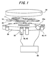
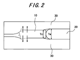
- the wafer polishing method of the present invention has a round hole 11 for holding a wafer 20, and the surface of a pair of polishing pads 30 positioned above and below a carrier 10 that is thinner than the wafer 20.
- a polishing liquid (not shown) is supplied to 30 a, and the polishing pad 30 is slid relative to the carrier 10 to simultaneously polish both surfaces of the wafer 20 held on the carrier 10. Is the method.
- the thickness of the wafer 20 is determined by detecting information generated by the carrier 10 due to the difference between the thickness of the carrier 10 and the thickness of the wafer 20 reaching a predetermined value, and the polishing is completed. It is characterized by making it.
- the carrier 10 due to the difference between the thickness T W of the thickness T C and the wafer 20 reaches a predetermined value of the carrier 10 (in Figure 2, the information generated by the vibration of the arrow direction of the carrier 10) emits information for by detecting the indexing thickness T W of the wafer, it is possible to terminate the polishing, the polishing amount of the wafer 20 As a result, the wafer 20 with reduced thickness variation after polishing can be obtained.
- FIG. 3 is a graph showing the intensity of information (sound and vibration) when the carrier is emitting information (here, it indicates sound and vibration) and when it is not, (A) is data about the sound which a carrier emits, (b) is data about the vibration which a carrier emits.
- the portions surrounded by broken lines in FIGS. 3 (a) and 3 (b) show the situation where sound and vibration are generated from the carrier. It can also be seen that the intensity of vibration is large. Therefore, for example, by grasping in advance the sound and vibration when the wafer 20 has a desired thickness and finishing the polishing when the sound and vibration are reached, the polishing can be controlled accurately. .
- the end of the polishing is set to 2 obtained from information obtained by acquiring information generated by the carrier 10 due to the difference between the thickness of the carrier 10 and the thickness of the wafer 20 reaching a predetermined value.
- the first signal and the second signal which are signals in various frequency domains, and detecting that the intensity of the first signal is equal to or higher than a predetermined value and the intensity of the second signal is equal to or lower than the predetermined value, polishing is performed. It is preferable to determine the end point.
- the first signal and the second signal extracted from the information are information obtained by the carrier 10 and are two kinds of signals having different frequency domains extracted from the acquired information by a predetermined process.
- a signal having a high frequency is a first signal
- a signal having a low frequency is a second signal.
- the frequency of each of the first signal and the second signal is not particularly limited as long as the polishing end point can be controlled by a combination of the first signal and the second signal. Can do.
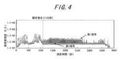
- FIG. 4 shows the intensity of two types of frequency domain signals (first signal and second signal) extracted from the elapsed time (seconds) and information (vibration) generated by the carrier 10 when polishing is performed. It is the graph which showed the relationship with (AU).
- the intensity of both the first signal and the second signal fluctuates before noise is generated from the carrier, but the intensity of the first signal increases when noise is generated.
- the intensity of the second signal remains small. Therefore, if the intensity (predetermined value) that the first signal should exceed and the intensity (predetermined value) that the second signal should decrease are set in advance, the polishing end point can be determined quantitatively.
- FIG. 4 shows the intensity of two types of frequency domain signals (first signal and second signal) extracted from the elapsed time (seconds) and information (vibration) generated by the carrier 10 when polishing is performed. It is the graph which showed the relationship with (AU).
- the intensity of both the first signal and the second signal fluctuates before noise is generated from the carrier, but the intensity of the first signal increases when noise is
- FIG. 5 is a graph showing the relationship between the elapsed time (seconds) and the intensity (m / s 2 ) of the vibration signal emitted from the carrier when polishing is performed. It is impossible to grasp the timing of noise generation from the above-mentioned carrier because many peaks of the same size are seen only by detection (0 to 480 seconds, 700 to 1000 seconds). The end point of polishing cannot be determined.
- the information which the carrier 10 is emitted as long as information that can determine the thickness T W of the wafer not particularly limited, for example, the carrier emits sound, vibration or the heat or the like is conceivable, facilitating It is preferable that the sound and / or vibration generated from the carrier 10 be able to reliably detect the polishing end point of the wafer 20.
- the method for extracting the signal from the information is not particularly limited as long as it can effectively extract the first signal and the second signal described above.
- desired signal data can be obtained relatively easily. Therefore, it is preferable to calculate the power spectrum for the digital data obtained by A / D converting the detected information and calculate the average value or the maximum value of the power spectrum signal intensity in the set frequency region. If necessary, the information can be filtered to A / D convert only a specific frequency, or a peak holding process can be performed after the filtering.
- the difference between the thickness T W of the thickness T C and the wafer 20 of the carrier 10 (T C -T W), the rotational speed of the polishing pad 30 Ya Although it varies depending on the pressure, the type of polishing liquid, etc., it is preferably in the range of 0.1 to 20 ⁇ m from the viewpoint that the polishing amount can be controlled more accurately.
- a detection sensor 40 installed in the vicinity of the carrier 10, for example, as shown in FIG.
- the detection sensor 40 include a sound detection microphone 41 and a vibration detection sensor 42 as shown in FIG.
- the frequency is preferably in the range of 10 to 1000 Hz. This is because it is considered that the sound range is suitable for grasping the end point of polishing, and when a sound outside the above range is detected to end polishing, there is a possibility that a desired wafer thickness cannot be obtained. Because. More preferably, the frequency range of the first signal is in the range of 200 to 1000 Hz, and the frequency range of the second signal is in the range of 10 to 200 Hz. If the first signal and the second signal are in these wavelength ranges, when noise is generated from the carrier 10, the difference in signal intensity differs greatly, so that the polishing end point is reliably determined. Because it can.
- the detected sound and / or vibration generated by the carrier 10 is converted into a signal and sent to the control device 60 as shown in FIG. 1, and the control device 60 extracts the first signal and the second signal. It is possible to determine whether to continue or end the polishing.
- the carrier 10 used in the polishing method of the present invention is a member for holding the wafer 20 to be polished, has a round hole for holding the wafer 20, and has a thickness T. C is thinner than the thickness T W of the wafer 20.
- the shape and material of the carrier 10 are not particularly limited, and a carrier used for normal double-side polishing of the wafer 20 can be used.
- the material of the carrier 10 is preferably a material having high wear resistance, a low coefficient of friction with the polishing pad, and high acid resistance or alkali resistance.
- a fiber reinforced plastic in which a reinforcing fiber such as a glass fiber, a carbon fiber, or an aramid fiber is combined with a resin such as an epoxy resin, a phenol resin, or a polyimide resin can be used.
- the polishing pad 30 is a member for simultaneously polishing both surfaces of the wafer 20 by sliding the wafer 20 from above and below.
- the material of the polishing pad 30 is preferably a material having a small coefficient of friction between the wafer 20 and the carrier 10.
- a urethane material having a hardness (Shore D) of 75 to 85 and a compression rate of 2 to 3% can be employed.
- the polishing pad 30 is preferably a polishing pad having fixed abrasive grains.
- the fixed abrasive means a solid that is fixed to the surface of the polishing pad and has a different material from the base material of the polishing pad.
- ceramics such as silica and alumina, simple substances such as diamond and silicon carbide, etc. Or what consists of high molecular polymers, such as compounds or polyethylene, a polypropylene, etc. can be used.
- the shape is not limited to a particle shape, and may be a solid or a gel.
- any of those prepared by a dry method (combustion method / arc method) or a wet method (precipitation method / sol-gel method) can be used as the kind of the silica.
- the polishing liquid used in the polishing method of the present invention is preferably a polishing liquid that does not contain abrasive grains. This is because, when a polishing liquid containing abrasive grains is used, it is difficult to detect information from the carrier 10 that is necessary for the end of polishing.
- the above-mentioned “polishing liquid not containing abrasive grains” inevitably includes polishing components that are contained in the polishing liquid, but does not actively contain the abrasive grains ingredients. Refers to liquid.
- FIG. 6 shows polishing time (min) and carrier thickness variation rate (%) when the carrier is polished using a polishing liquid containing abrasive grains and a polishing liquid not containing abrasive grains, respectively. It is the graph which showed the relationship.
- FIG. 6 shows that the amount of carrier wear is large when a polishing liquid containing abrasive grains is used.
- the type of the polishing liquid is not particularly limited, but it is preferable to use, for example, an alkaline aqueous solution whose pH is adjusted within the range of 8-14. When the pH is less than 8, the etching action is low and the polishing rate is lowered. On the other hand, when the pH exceeds 14, the handling of the polishing liquid becomes difficult.
- an alkaline aqueous solution an aqueous ammonia solution, an alkaline hydroxide aqueous solution such as potassium hydroxide or sodium hydroxide, or an alkaline carbonate aqueous solution can be employed.
- aqueous solutions of hydrazine and amines can be employed.
- the polishing liquid preferably contains a predetermined polymer component. This is because noise (squeal) generated from the carrier 10 can be further reduced.
- the type of the polymer component is not particularly limited, but it is preferable to use hydroxyethyl cellulose or polyethylene glycol. In particular, since hydroxyethyl cellulose has a relatively large molecular weight, the friction coefficient between the polishing pad 30 and the carrier 10 can be efficiently reduced by the bearing action between the polishing pad 30 and the carrier 10, and as a result. The occurrence of defects on the surface of the polished wafer can be suppressed.
- the concentration of the polymer component added to the polishing liquid is preferably in the range of 0.01 ppm to 1000 ppm. This is because when the concentration of the polymer component is less than 0.01 ppm, the friction coefficient during polishing becomes large, and defects may occur on the surface of the wafer after polishing. This is because the rate is extremely lowered and a great amount of time is required for mirror polishing.
- a chelating agent to the polishing liquid from the viewpoint of removing metal ions contained in the polishing liquid.
- the type of chelating agent is not particularly limited as long as it is a substance having a chelating ability for metal ions.
- phosphonic acid-based chelating agents, aminocarboxylic acid-based chelating agents, and the like can be used, but aminocarboxylic acid-based chelating agents are desirable in consideration of solubility in an alkaline aqueous solution.
- aminocarboxylates such as ethylenediaminetetraacetic acid (EDTA: Ethylene Diatetraacetic Acid) or diethylenetriaminepentaacetic acid (DTPA) are more preferable.
- concentration of the chelating agent is preferably in the range of 0.1 ppm to 1000 ppm, whereby metal ions such as Cu, Zn, Fe, Cr, Ni, and Al can be captured.
- the surface of the silicon wafer 20 is polished by sliding the polishing pad 30 relative to the carrier 10.
- the sliding method is not particularly limited, and the sliding may be performed by moving only the polishing pad 30 or only the carrier 10, or both the polishing pad 30 and the carrier 10 may be relatively moved. You may make it slide by moving to.
- the pressure applied to the polishing pad 30 in the direction perpendicular to the surface of the wafer 20 is preferably in the range of 100 to 300 g / cm 2 . If it is less than 100 g / cm 2, since the pressure is too small, the information is the carrier 10 of the sound or vibration emitted is because there may not be sufficiently obtained, while when it exceeds 300 g / cm 2, the pressure This is because it is too large, and the sound and vibration of the carrier 10 are likely to be generated, and there is a possibility that the polishing end point of the wafer 20 cannot be accurately grasped.
- Example 1 As Example 1, as shown in FIG. 1, a pair of urethane polishing pads 30 having a round hole 11 for holding a wafer 20 and positioned above and below a carrier 10 having a thickness of 750 ⁇ m thinner than that of the wafer 20.
- a polishing liquid not containing abrasive grains is supplied to the surface (potassium hydroxide aqueous solution added with ethylenediaminetetraacetic acid having a concentration of 10 ppm as a chelating agent and hydroxyethylcellulose having a concentration of 1 ppm as a polymer component), and the polishing is performed on the carrier.
- the silicon wafer 20 having a diameter of 300 mm was polished by a wafer polishing method in which both surfaces of the wafer held on the carrier were simultaneously polished by sliding the pad relatively.
- the determination of the polishing end point is obtained by acquiring the vibration generated from each carrier 10 by the vibration detection sensor 42 installed in the outer gear 50, and from the obtained vibration, the first signal (average value of 200 to 1000 Hz) and the second signal ( (Average value of 10 to 100 Hz) is extracted, and the intensity of the first signal is equal to or higher than a predetermined value (0.02 AU) and the intensity of the second signal is equal to or lower than a predetermined value (0.02 AU). It was done by detecting that.
- Table 1 shows each polishing condition (type of polishing liquid, presence / absence of polymer component in polishing liquid, and detection method of polishing end point).
- the silicon wafer was polished a total of 5 times (25 sheets).
- Example 2 In the second embodiment, the sound emitted from each carrier 10 is acquired by the sound detection microphone 41 installed in the vicinity of each carrier 10, and the first signal (480 Hz) and the second signal (100 Hz) are extracted from the obtained sound. Except for the above, the silicon wafer (25 sheets) was polished by the same method as in Example 1. Table 1 shows each polishing condition (type of polishing liquid, presence / absence of polymer in polishing liquid and detection method of polishing end point).
- Comparative Example 1 As Comparative Example 1, a silicon wafer (25 sheets) was formed under the same conditions as in Example 1 except that a polishing liquid containing abrasive grains (potassium hydroxide aqueous solution containing colloidal silica as free abrasive grains) was used. Polishing was performed. Table 1 shows each polishing condition (type of polishing liquid, presence / absence of polymer component in polishing liquid, and detection method of polishing end point).
- Comparative Example 2 As Comparative Example 2, the silicon wafer (25 sheets) was polished under the same conditions as in Example 1 except that the polishing was controlled not by the information (sound or vibration) generated by the carrier but by the set time. .
- Table 1 shows each polishing condition (type of polishing liquid, presence / absence of polymer component in polishing liquid, and detection method of polishing end point).
- the present invention it is possible to provide a silicon wafer polishing method capable of suppressing noise generated from a carrier and further reducing variation in the thickness of the wafer after polishing.
Landscapes
- Engineering & Computer Science (AREA)
- Mechanical Engineering (AREA)
- Mechanical Treatment Of Semiconductor (AREA)
- Finish Polishing, Edge Sharpening, And Grinding By Specific Grinding Devices (AREA)
Abstract
Description
一方、ウェーハの両面を同時に研磨する際の研磨液として、砥粒を含まない研磨液を用いる場合、金属製のキャリア、金属板の表裏面に樹脂をコーティングしたキャリア、または樹脂製のキャリアの何れのキャリアを使用した場合においても、キャリアの磨耗が抑制できるが、研磨が進行するにつれてキャリアの厚さとウェーハの厚さとの差が小さくなったときに、研磨パッドがキャリアに接触してキャリアを振動させる結果、キャリアから騒音が発生するという問題がある。
(1)ウェーハを保持する丸孔を有し、厚さがウェーハよりも薄いキャリアの上下に位置する一対の研磨パッドの表面に、研磨液を供給し、前記キャリアに対し前記研磨パッドを相対的に摺動させることで、前記キャリアに保持したウェーハの両面を同時に研磨するウェーハの研磨方法であって、前記キャリアの厚さと前記ウェーハの厚さとの差が所定値に到達することに起因して前記キャリアが発する情報を検出することで、前記ウェーハの厚さを割り出し、研磨を終了させることを特徴とするウェーハの研磨方法。
本発明のウェーハの研磨方法は、図1に示すように、ウェーハ20を保持する丸孔11を有し、厚さがウェーハ20よりも薄いキャリア10の上下に位置する一対の研磨パッド30の表面30aに、研磨液(図示せず)を供給し、前記キャリア10に対し前記研磨パッド30を相対的に摺動させることで、前記キャリア10に保持したウェーハ20の両面を同時に研磨するウェーハの研磨方法である。
一方、図5は、研磨を行った際の、経過時間(秒)と、キャリアから発せられた振動信号の強度(m/s2)との関係を示したグラフであるが、ただ振動信号を検出しただけでは、同程度の大きさのピークが多数見られる(0~480秒、700~1000秒)ことから、上述のキャリアからの騒音が発生するタイミングを把握することは不可能であり、研磨の終点を判定することはできない。
また、前記第1信号の周波数領域は、200~1000Hzの範囲であること、前記第2信号の周波数領域は、10~200Hzの範囲であることがより好ましい。前記第1信号及び第2信号が、これらの波長範囲であれば、前記キャリア10から騒音が発生した際に、それぞれの信号強度の差が大きく異なるため、確実に研磨の終了点の判定を行うことができるからである。
実施例1として、図1に示すように、ウェーハ20を保持する丸孔11を有し、厚さがウェーハ20よりも薄い750μmであるキャリア10の上下に位置する一対のウレタン製研磨パッド30の表面に、砥粒を含まない研磨液(キレート剤として濃度が10ppmのエチレンジアミン四酢酸、高分子成分として濃度が1ppmのヒドロキシエチルセルロースを添加した水酸化カリウム水溶液)を供給し、前記キャリアに対し前記研磨パッドを相対的に摺動させることで、前記キャリアに保持したウェーハの両面を同時に研磨するウェーハの研磨方法によって、直径300mmのシリコンウェーハ20の研磨を行った。 研磨終点の判定は、各キャリア10から発する振動を、アウターギア50に設置された振動検出センサ42によって取得し、得られた振動から第1信号(200~1000Hzの平均値)及び第2信号(10~100Hzの平均値)を抽出し、第1信号の強度が所定値(0.02A.U.)以上で、かつ第2信号の強度が所定値(0.02A.U.)以下となることを検出することで行った。
研磨の各条件(研磨液の種類、研磨液中の高分子成分の有無及び研磨終点の検出方法)については、表1に示す。また、シリコンウェーハの研磨は、計5回(25枚)行った。
実施例2は、各キャリア10から発する音を、各キャリア10の近傍に設置された音検出マイク41によって取得し、得られた音から第1信号(480Hz)及び第2信号(100Hz)を抽出したこと以外は、実施例1と同様の方法によって、シリコンウェーハ(25枚)の研磨を行った。
研磨の各条件(研磨液の種類、研磨液中の高分子の有無及び研磨終点の検出方法)については、表1に示す。
比較例1として、砥粒を含んだ研磨液(コロイダルシリカを遊離砥粒として含有した水酸化カリウム水溶液)を用いたこと以外は、実施例1と同様の条件によって、シリコンウェーハ(25枚)の研磨を行った。
研磨の各条件(研磨液の種類、研磨液中の高分子成分の有無及び研磨終点の検出方法)については、表1に示す。
比較例2として、キャリアが発する情報(音又は振動)ではなく、設定時間によって研磨の制御を行ったこと以外は、実施例1と同様の条件によって、シリコンウェーハ(25枚)の研磨を行った。
研磨の各条件(研磨液の種類、研磨液中の高分子成分の有無及び研磨終点の検出方法)については、表1に示す。
(1)キャリアの磨耗について
実施例1及び比較例1について、研磨前、研磨開始から所定時間経過後及び研磨終了後のキャリアの厚さTCを測定し、研磨時間とキャリアの厚さTCとの関係をプロットすることによって、キャリアの磨耗度についての評価を行った。その結果を図6及び表1に示す。
実施例及び比較例によって得られた各シリコンウェーハについて、KLA−Tencor社製のWaferSightを用いて、ウェーハの厚さ分布を測定し、各ウェーハの厚さのバラツキを算出した。そして、全ウェーハの平均値を算出することによって、厚さのバラツキの評価を行った。評価の結果は表1に示すとおりで、小さいほど良好な結果である。

11 丸孔
20 ウェーハ、シリコンウェーハ
30 研磨パッド
40 検出センサ
41 音検出マイク
42 振動検出センサ
50 アウターギア
60 制御装置
Claims (12)
- ウェーハを保持する丸孔を有し、厚さがウェーハよりも薄いキャリアの上下に位置する一対の研磨パッドの表面に、研磨液を供給し、前記キャリアに対し前記研磨パッドを相対的に摺動させることで、前記キャリアに保持したウェーハの両面を同時に研磨するウェーハの研磨方法であって、
前記キャリアの厚さと前記ウェーハの厚さとの差が所定値に到達することに起因して前記キャリアが発する情報を検出することで、前記ウェーハの厚さを割り出し、研磨を終了させることを特徴とするウェーハの研磨方法。 - 前記研磨の終了は、前記キャリアから得られた情報を元に、設定した2種の周波数領域の信号である第1信号及び第2信号を抽出し、第1信号の強度が所定値以上で、かつ第2信号の強度が所定値以下となることを検出することで、研磨の終了点の判定を行うことを特徴とする請求項1に記載のウェーハの研磨方法。
- 前記研磨液は、砥粒を含まない研磨液であることを特徴とする請求項1に記載のウェーハの研磨方法。
- 前記キャリアが発する情報は、音及び/又は振動であることを特徴とする請求項1に記載のウェーハの研磨方法。
- 前記情報が発せられるときの、前記キャリアの厚さと前記ウェーハの厚さとの差は、0.1~20μmの範囲であることを特徴とする請求項1に記載のウェーハの研磨方法。
- 前記ウェーハの表面に対して垂直方向の前記研磨パッドに加える圧力は、100~300g/cm2の範囲であることを特徴とする請求項1に記載のウェーハの研磨方法。
- 前記キャリアが発する情報の検出は、キャリアごとに設置された検出センサによって行うことを特徴とする請求項1に記載のウェーハの研磨方法。
- 前記検出センサは、前記キャリアを保持するための機構に設置することを特徴とする請求項7に記載のウェーハの研磨方法。
- 前記検出センサは、前記キャリアを動かすためのアウターギアに設置することを特徴とする請求項8に記載のウェーハの研磨方法。
- 前記キャリアが発する音の検出は、周波数が10~1000Hzの範囲である音を検出することで行うことを特徴とする請求項4に記載のウェーハの研磨方法。
- 前記研磨液は、所定の高分子成分を含有することを特徴とする請求項1に記載のウェーハの研磨方法。
- 前記情報からの信号の抽出は、検出した情報をA/D変換したデジタルデータに対して、パワースペクトルを算出し、設定された周波数領域のパワースペクトル信号強度平均値もしくは最大値の算出であることを特徴とする請求項2に記載のウェーハの研磨方法。
Priority Applications (4)
| Application Number | Priority Date | Filing Date | Title |
|---|---|---|---|
| KR1020127017088A KR101409738B1 (ko) | 2009-12-01 | 2010-11-30 | 웨이퍼의 연마 방법 |
| JP2011544345A JP5533884B2 (ja) | 2009-12-01 | 2010-11-30 | ウェーハの研磨方法 |
| DE112010004635.2T DE112010004635B4 (de) | 2009-12-01 | 2010-11-30 | Wafer-Polierverfahren |
| US13/261,294 US8900033B2 (en) | 2009-12-01 | 2010-11-30 | Wafer polishing method |
Applications Claiming Priority (4)
| Application Number | Priority Date | Filing Date | Title |
|---|---|---|---|
| JP2009273255 | 2009-12-01 | ||
| JP2009-273255 | 2009-12-01 | ||
| JP2009-276517 | 2009-12-04 | ||
| JP2009276517 | 2009-12-04 |
Publications (1)
| Publication Number | Publication Date |
|---|---|
| WO2011068236A1 true WO2011068236A1 (ja) | 2011-06-09 |
Family
ID=44115078
Family Applications (1)
| Application Number | Title | Priority Date | Filing Date |
|---|---|---|---|
| PCT/JP2010/071777 Ceased WO2011068236A1 (ja) | 2009-12-01 | 2010-11-30 | ウェーハの研磨方法 |
Country Status (6)
| Country | Link |
|---|---|
| US (1) | US8900033B2 (ja) |
| JP (1) | JP5533884B2 (ja) |
| KR (1) | KR101409738B1 (ja) |
| DE (1) | DE112010004635B4 (ja) |
| TW (1) | TWI434338B (ja) |
| WO (1) | WO2011068236A1 (ja) |
Cited By (2)
| Publication number | Priority date | Publication date | Assignee | Title |
|---|---|---|---|---|
| JP2017163100A (ja) * | 2016-03-11 | 2017-09-14 | 東芝メモリ株式会社 | 半導体製造装置の制御装置および制御方法 |
| CN112405326A (zh) * | 2020-10-20 | 2021-02-26 | 上海中欣晶圆半导体科技有限公司 | 一种检测研磨载体厚度及保证研磨载体厚度均匀的方法 |
Families Citing this family (4)
| Publication number | Priority date | Publication date | Assignee | Title |
|---|---|---|---|---|
| US8900033B2 (en) * | 2009-12-01 | 2014-12-02 | Sumco Corporation | Wafer polishing method |
| JP6437608B1 (ja) * | 2017-09-08 | 2018-12-12 | 東芝メモリ株式会社 | 研磨装置、研磨方法、および研磨制御装置 |
| US11565365B2 (en) * | 2017-11-13 | 2023-01-31 | Taiwan Semiconductor Manufacturing Co., Ltd. | System and method for monitoring chemical mechanical polishing |
| CN116214360A (zh) * | 2023-02-03 | 2023-06-06 | 中国特种设备检测研究院 | 游星轮、试样的处理方法及装置、存储介质和电子设备 |
Citations (6)
| Publication number | Priority date | Publication date | Assignee | Title |
|---|---|---|---|---|
| JPH09139369A (ja) * | 1995-11-15 | 1997-05-27 | Hitachi Ltd | 半導体装置の製造方法およびそれに使用される研磨装置 |
| JPH09150367A (ja) * | 1995-04-26 | 1997-06-10 | Fujitsu Ltd | 研磨装置及び研磨方法 |
| JP2001007063A (ja) * | 1999-06-22 | 2001-01-12 | Mitsubishi Materials Silicon Corp | シリコンウェーハの研磨方法及びこの方法により研磨されたシリコンウェーハ |
| JP2005501410A (ja) * | 2001-08-21 | 2005-01-13 | キャボット マイクロエレクトロニクス コーポレイション | 周波数解析に基づく監視を含むcmpプロセス |
| JP2005252000A (ja) * | 2004-03-04 | 2005-09-15 | Kashiwara Machine Mfg Co Ltd | ウエーハ研磨方法 |
| WO2009041697A1 (ja) * | 2007-09-28 | 2009-04-02 | Nitta Haas Incorporated | 研磨用組成物 |
Family Cites Families (36)
| Publication number | Priority date | Publication date | Assignee | Title |
|---|---|---|---|---|
| US3097458A (en) * | 1960-05-13 | 1963-07-16 | Method of accurately machining semiconductor bodies | |
| US3093937A (en) * | 1962-11-30 | 1963-06-18 | Cavitron Ultrasonics Inc | Ultrasonic lapping machines |
| DE1215549B (de) * | 1963-03-15 | 1966-04-28 | Sebastian Messerschmidt | Leiteinrichtung fuer eine Vorrichtung zum Laeppen und Schleifen von Kugeln |
| US3579922A (en) * | 1968-10-11 | 1971-05-25 | Western Electric Co | Apparatus for abrading articles |
| US4197676A (en) * | 1978-07-17 | 1980-04-15 | Sauerland Franz L | Apparatus for automatic lapping control |
| JPS55106769A (en) * | 1979-01-31 | 1980-08-15 | Masami Masuko | Lapping method and its apparatus |
| JPS6362673A (ja) * | 1986-09-01 | 1988-03-18 | Speedfam Co Ltd | 定寸機構付き平面研磨装置 |
| JP3198525B2 (ja) | 1991-03-28 | 2001-08-13 | ソニー株式会社 | ポリッシュ装置、ポリッシュ方法、及び半導体装置の製造方法 |
| US5222329A (en) * | 1992-03-26 | 1993-06-29 | Micron Technology, Inc. | Acoustical method and system for detecting and controlling chemical-mechanical polishing (CMP) depths into layers of conductors, semiconductors, and dielectric materials |
| JP3083919B2 (ja) | 1992-07-21 | 2000-09-04 | 日本碍子株式会社 | 電子部品熱処理用冶具 |
| JPH0645299U (ja) | 1992-11-27 | 1994-06-14 | 株式会社カンセイ | 高輝度放電灯点灯回路 |
| US5876265A (en) | 1995-04-26 | 1999-03-02 | Fujitsu Limited | End point polishing apparatus and polishing method |
| JP3894367B2 (ja) * | 1995-04-26 | 2007-03-22 | 富士通株式会社 | 研磨装置 |
| JPH10180624A (ja) * | 1996-12-19 | 1998-07-07 | Shin Etsu Handotai Co Ltd | ラッピング装置及び方法 |
| US5882245A (en) * | 1997-02-28 | 1999-03-16 | Advanced Ceramics Research, Inc. | Polymer carrier gears for polishing of flat objects |
| JPH11114813A (ja) * | 1997-10-07 | 1999-04-27 | Speedfam Co Ltd | 研磨システム及びその制御方法 |
| JPH11277421A (ja) * | 1998-03-31 | 1999-10-12 | Speedfam Co Ltd | ワークの装填方法及びワークの位置ずれ修正機構付き平面研磨装置 |
| JP3292243B2 (ja) | 1999-06-30 | 2002-06-17 | 日本電気株式会社 | 研磨終点検出装置 |
| US6210259B1 (en) * | 1999-11-08 | 2001-04-03 | Vibro Finish Tech Inc. | Method and apparatus for lapping of workpieces |
| US6709981B2 (en) | 2000-08-16 | 2004-03-23 | Memc Electronic Materials, Inc. | Method and apparatus for processing a semiconductor wafer using novel final polishing method |
| US6416392B1 (en) * | 2000-11-30 | 2002-07-09 | Seh America, Inc. | Sound enhanced lapping process |
| US20040248415A1 (en) * | 2002-02-20 | 2004-12-09 | Yutaka Wada | Polishing method and polishing liquid |
| JP2004071833A (ja) * | 2002-08-06 | 2004-03-04 | Sumitomo Mitsubishi Silicon Corp | 半導体ウェーハの両面研磨方法 |
| JP4219718B2 (ja) * | 2003-03-28 | 2009-02-04 | Hoya株式会社 | Euvマスクブランクス用ガラス基板の製造方法及びeuvマスクブランクスの製造方法 |
| JP2006231470A (ja) * | 2005-02-25 | 2006-09-07 | Speedfam Co Ltd | 両面ポリッシュ加工機の定寸方法及び定寸装置 |
| JP2006231471A (ja) * | 2005-02-25 | 2006-09-07 | Speedfam Co Ltd | 両面ポリッシュ加工機とその定寸制御方法 |
| JP2006303136A (ja) | 2005-04-20 | 2006-11-02 | Shin Etsu Handotai Co Ltd | 両面研磨装置用キャリア及びこれを用いた両面研磨装置並びに両面研磨方法 |
| JP4820108B2 (ja) * | 2005-04-25 | 2011-11-24 | コマツNtc株式会社 | 半導体ウエーハの製造方法およびワークのスライス方法ならびにそれらに用いられるワイヤソー |
| DE102007056628B4 (de) * | 2007-03-19 | 2019-03-14 | Siltronic Ag | Verfahren und Vorrichtung zum gleichzeitigen Schleifen mehrerer Halbleiterscheiben |
| JP5245319B2 (ja) * | 2007-08-09 | 2013-07-24 | 富士通株式会社 | 研磨装置及び研磨方法、基板及び電子機器の製造方法 |
| WO2009098951A1 (ja) | 2008-02-07 | 2009-08-13 | Jsr Corporation | 化学機械研磨用水系分散体、および該分散体を調製するためのキット、該キットを用いた化学機械研磨用水系分散体の調製方法、ならびに半導体装置の化学機械研磨方法 |
| JP2011519735A (ja) * | 2008-04-21 | 2011-07-14 | アプライド マテリアルズ インコーポレイテッド | 研磨中に基板縁部の厚さを測定する方法および装置 |
| JP5407693B2 (ja) * | 2009-09-17 | 2014-02-05 | 旭硝子株式会社 | ガラス基板の製造方法、研磨方法及び研磨装置、並びにガラス基板 |
| US8900033B2 (en) * | 2009-12-01 | 2014-12-02 | Sumco Corporation | Wafer polishing method |
| DE112011102297B4 (de) * | 2010-07-08 | 2020-10-08 | Sumco Corporation | Verfahren zum Polieren von Siliziumwafern |
| JP2012205258A (ja) * | 2011-03-28 | 2012-10-22 | Seiko Instruments Inc | 研磨方法、圧電振動片の製造方法、圧電振動子、発振器、電子機器及び電波時計 |
-
2010
- 2010-11-30 US US13/261,294 patent/US8900033B2/en active Active
- 2010-11-30 JP JP2011544345A patent/JP5533884B2/ja active Active
- 2010-11-30 KR KR1020127017088A patent/KR101409738B1/ko active Active
- 2010-11-30 WO PCT/JP2010/071777 patent/WO2011068236A1/ja not_active Ceased
- 2010-11-30 DE DE112010004635.2T patent/DE112010004635B4/de active Active
- 2010-12-01 TW TW099141784A patent/TWI434338B/zh active
Patent Citations (6)
| Publication number | Priority date | Publication date | Assignee | Title |
|---|---|---|---|---|
| JPH09150367A (ja) * | 1995-04-26 | 1997-06-10 | Fujitsu Ltd | 研磨装置及び研磨方法 |
| JPH09139369A (ja) * | 1995-11-15 | 1997-05-27 | Hitachi Ltd | 半導体装置の製造方法およびそれに使用される研磨装置 |
| JP2001007063A (ja) * | 1999-06-22 | 2001-01-12 | Mitsubishi Materials Silicon Corp | シリコンウェーハの研磨方法及びこの方法により研磨されたシリコンウェーハ |
| JP2005501410A (ja) * | 2001-08-21 | 2005-01-13 | キャボット マイクロエレクトロニクス コーポレイション | 周波数解析に基づく監視を含むcmpプロセス |
| JP2005252000A (ja) * | 2004-03-04 | 2005-09-15 | Kashiwara Machine Mfg Co Ltd | ウエーハ研磨方法 |
| WO2009041697A1 (ja) * | 2007-09-28 | 2009-04-02 | Nitta Haas Incorporated | 研磨用組成物 |
Cited By (3)
| Publication number | Priority date | Publication date | Assignee | Title |
|---|---|---|---|---|
| JP2017163100A (ja) * | 2016-03-11 | 2017-09-14 | 東芝メモリ株式会社 | 半導体製造装置の制御装置および制御方法 |
| US10553507B2 (en) | 2016-03-11 | 2020-02-04 | Toshiba Memory Corporation | Control device and control method of semiconductor manufacturing apparatus |
| CN112405326A (zh) * | 2020-10-20 | 2021-02-26 | 上海中欣晶圆半导体科技有限公司 | 一种检测研磨载体厚度及保证研磨载体厚度均匀的方法 |
Also Published As
| Publication number | Publication date |
|---|---|
| DE112010004635T5 (de) | 2012-10-04 |
| TW201126587A (en) | 2011-08-01 |
| KR101409738B1 (ko) | 2014-07-02 |
| JPWO2011068236A1 (ja) | 2013-04-22 |
| JP5533884B2 (ja) | 2014-06-25 |
| US8900033B2 (en) | 2014-12-02 |
| DE112010004635B4 (de) | 2019-03-21 |
| KR20120096061A (ko) | 2012-08-29 |
| US20130017763A1 (en) | 2013-01-17 |
| TWI434338B (zh) | 2014-04-11 |
Similar Documents
| Publication | Publication Date | Title |
|---|---|---|
| JP5533884B2 (ja) | ウェーハの研磨方法 | |
| JP5995825B2 (ja) | 少なくとも1つのウエハを研磨する方法 | |
| CN102049723B (zh) | 抛光半导体晶片的方法 | |
| US8388411B2 (en) | Method for polishing the edge of a semiconductor wafer | |
| CN104064455B (zh) | 半导体材料晶片的抛光方法 | |
| CN1307279C (zh) | 基板的制造方法 | |
| CN102205520B (zh) | 双面抛光半导体晶片的方法 | |
| CN107529477B (zh) | 微晶玻璃化学机械抛光方法及微晶玻璃 | |
| KR20030024879A (ko) | 신규한 최종 연마 방법을 사용하여 반도체 웨이퍼를처리하기 위한 방법 및 장치 | |
| CN111316399B (zh) | 半导体晶片的制造方法 | |
| JP2006080329A (ja) | 化学的機械的研磨装置 | |
| JP6747376B2 (ja) | シリコンウエーハの研磨方法 | |
| KR101767059B1 (ko) | 화학 기계적 기판 연마장치 | |
| JP5982427B2 (ja) | 両面加工装置に用いられるキャリアプレート | |
| JP2015129056A (ja) | ガラス基板の切断方法及び磁気記録媒体用ガラス基板の製造方法 | |
| JP2004055128A (ja) | 磁気記録媒体用ガラスディスク基板の製造方法 | |
| JP5613723B2 (ja) | キャリアプレートおよび円盤状基板の製造方法、円盤状基板の両面加工装置 | |
| JP2010021391A (ja) | シリコンウェーハの研磨方法 | |
| KR101133355B1 (ko) | 반도체 웨이퍼의 연마 방법 | |
| JP7738401B2 (ja) | 研磨パッド及びウェハ研磨方法 | |
| JP5942774B2 (ja) | ガラス基板の研磨方法 | |
| JP4210134B2 (ja) | ウエーハ研磨治具及びその製造方法 | |
| JP2011035321A (ja) | Cmp装置 | |
| JP4598551B2 (ja) | 被加工物保持材および被加工物保持材の製造方法 | |
| CN104325389A (zh) | 磁记录介质用玻璃基板的研磨方法以及制造方法 |
Legal Events
| Date | Code | Title | Description |
|---|---|---|---|
| 121 | Ep: the epo has been informed by wipo that ep was designated in this application |
Ref document number: 10834683 Country of ref document: EP Kind code of ref document: A1 |
|
| WWE | Wipo information: entry into national phase |
Ref document number: 2011544345 Country of ref document: JP |
|
| WWE | Wipo information: entry into national phase |
Ref document number: 13261294 Country of ref document: US |
|
| WWE | Wipo information: entry into national phase |
Ref document number: 112010004635 Country of ref document: DE Ref document number: 1120100046352 Country of ref document: DE |
|
| ENP | Entry into the national phase |
Ref document number: 20127017088 Country of ref document: KR Kind code of ref document: A |
|
| 122 | Ep: pct application non-entry in european phase |
Ref document number: 10834683 Country of ref document: EP Kind code of ref document: A1 |