WO2011058786A1 - 色素増感型太陽電池 - Google Patents
色素増感型太陽電池 Download PDFInfo
- Publication number
- WO2011058786A1 WO2011058786A1 PCT/JP2010/061488 JP2010061488W WO2011058786A1 WO 2011058786 A1 WO2011058786 A1 WO 2011058786A1 JP 2010061488 W JP2010061488 W JP 2010061488W WO 2011058786 A1 WO2011058786 A1 WO 2011058786A1
- Authority
- WO
- WIPO (PCT)
- Prior art keywords
- dye
- solar cell
- sensitized solar
- substrate
- porous layer
- Prior art date
- Legal status (The legal status is an assumption and is not a legal conclusion. Google has not performed a legal analysis and makes no representation as to the accuracy of the status listed.)
- Ceased
Links
Images


Classifications
-
- H—ELECTRICITY
- H01—ELECTRIC ELEMENTS
- H01G—CAPACITORS; CAPACITORS, RECTIFIERS, DETECTORS, SWITCHING DEVICES, LIGHT-SENSITIVE OR TEMPERATURE-SENSITIVE DEVICES OF THE ELECTROLYTIC TYPE
- H01G9/00—Electrolytic capacitors, rectifiers, detectors, switching devices, light-sensitive or temperature-sensitive devices; Processes of their manufacture
- H01G9/20—Light-sensitive devices
- H01G9/2095—Light-sensitive devices comprising a flexible sustrate
-
- H—ELECTRICITY
- H01—ELECTRIC ELEMENTS
- H01G—CAPACITORS; CAPACITORS, RECTIFIERS, DETECTORS, SWITCHING DEVICES, LIGHT-SENSITIVE OR TEMPERATURE-SENSITIVE DEVICES OF THE ELECTROLYTIC TYPE
- H01G9/00—Electrolytic capacitors, rectifiers, detectors, switching devices, light-sensitive or temperature-sensitive devices; Processes of their manufacture
- H01G9/20—Light-sensitive devices
- H01G9/2022—Light-sensitive devices characterized by he counter electrode
-
- H—ELECTRICITY
- H01—ELECTRIC ELEMENTS
- H01G—CAPACITORS; CAPACITORS, RECTIFIERS, DETECTORS, SWITCHING DEVICES, LIGHT-SENSITIVE OR TEMPERATURE-SENSITIVE DEVICES OF THE ELECTROLYTIC TYPE
- H01G9/00—Electrolytic capacitors, rectifiers, detectors, switching devices, light-sensitive or temperature-sensitive devices; Processes of their manufacture
- H01G9/20—Light-sensitive devices
- H01G9/2027—Light-sensitive devices comprising an oxide semiconductor electrode
-
- H—ELECTRICITY
- H01—ELECTRIC ELEMENTS
- H01G—CAPACITORS; CAPACITORS, RECTIFIERS, DETECTORS, SWITCHING DEVICES, LIGHT-SENSITIVE OR TEMPERATURE-SENSITIVE DEVICES OF THE ELECTROLYTIC TYPE
- H01G9/00—Electrolytic capacitors, rectifiers, detectors, switching devices, light-sensitive or temperature-sensitive devices; Processes of their manufacture
- H01G9/20—Light-sensitive devices
- H01G9/2059—Light-sensitive devices comprising an organic dye as the active light absorbing material, e.g. adsorbed on an electrode or dissolved in solution
-
- H—ELECTRICITY
- H01—ELECTRIC ELEMENTS
- H01G—CAPACITORS; CAPACITORS, RECTIFIERS, DETECTORS, SWITCHING DEVICES, LIGHT-SENSITIVE OR TEMPERATURE-SENSITIVE DEVICES OF THE ELECTROLYTIC TYPE
- H01G9/00—Electrolytic capacitors, rectifiers, detectors, switching devices, light-sensitive or temperature-sensitive devices; Processes of their manufacture
- H01G9/20—Light-sensitive devices
- H01G9/2068—Panels or arrays of photoelectrochemical cells, e.g. photovoltaic modules based on photoelectrochemical cells
- H01G9/2077—Sealing arrangements, e.g. to prevent the leakage of the electrolyte
-
- H—ELECTRICITY
- H01—ELECTRIC ELEMENTS
- H01G—CAPACITORS; CAPACITORS, RECTIFIERS, DETECTORS, SWITCHING DEVICES, LIGHT-SENSITIVE OR TEMPERATURE-SENSITIVE DEVICES OF THE ELECTROLYTIC TYPE
- H01G9/00—Electrolytic capacitors, rectifiers, detectors, switching devices, light-sensitive or temperature-sensitive devices; Processes of their manufacture
- H01G9/20—Light-sensitive devices
- H01G9/2004—Light-sensitive devices characterised by the electrolyte, e.g. comprising an organic electrolyte
- H01G9/2009—Solid electrolytes
-
- H—ELECTRICITY
- H01—ELECTRIC ELEMENTS
- H01G—CAPACITORS; CAPACITORS, RECTIFIERS, DETECTORS, SWITCHING DEVICES, LIGHT-SENSITIVE OR TEMPERATURE-SENSITIVE DEVICES OF THE ELECTROLYTIC TYPE
- H01G9/00—Electrolytic capacitors, rectifiers, detectors, switching devices, light-sensitive or temperature-sensitive devices; Processes of their manufacture
- H01G9/20—Light-sensitive devices
- H01G9/2027—Light-sensitive devices comprising an oxide semiconductor electrode
- H01G9/2031—Light-sensitive devices comprising an oxide semiconductor electrode comprising titanium oxide, e.g. TiO2
-
- Y—GENERAL TAGGING OF NEW TECHNOLOGICAL DEVELOPMENTS; GENERAL TAGGING OF CROSS-SECTIONAL TECHNOLOGIES SPANNING OVER SEVERAL SECTIONS OF THE IPC; TECHNICAL SUBJECTS COVERED BY FORMER USPC CROSS-REFERENCE ART COLLECTIONS [XRACs] AND DIGESTS
- Y02—TECHNOLOGIES OR APPLICATIONS FOR MITIGATION OR ADAPTATION AGAINST CLIMATE CHANGE
- Y02E—REDUCTION OF GREENHOUSE GAS [GHG] EMISSIONS, RELATED TO ENERGY GENERATION, TRANSMISSION OR DISTRIBUTION
- Y02E10/00—Energy generation through renewable energy sources
- Y02E10/50—Photovoltaic [PV] energy
- Y02E10/542—Dye sensitized solar cells
Definitions
- the present invention relates to a dye-sensitized solar cell that is flexible and has no short circuit or other defects.
- a general dye-sensitized solar cell 100 includes a dye-sensitized solar cell substrate 110 in which a first electrode layer 112 is laminated on a substrate 111, and an electrode as an electrode.
- a porous layer 102 containing metal oxide semiconductor fine particles carrying a dye sensitizer and an electrolyte layer 101 are formed inside a sealing material 103 between a counter electrode substrate 120 having a function. is there.
- the dye sensitizer adsorbed on the surface of the metal oxide semiconductor fine particles in the porous layer 102 is excited by receiving sunlight from the substrate 111 side, and the excited electrons are conducted to the first electrode layer. And conducted to the counter electrode substrate through an external circuit. Thereafter, electricity is generated by returning the electrons to the ground level of the dye sensitizer through the redox pair.
- a glass substrate has been conventionally used as a base material.
- a substrate has been studied.
- the substrate is curved, whereby the first electrode layer and the counter electrode base material described above are in electrical contact with each other, causing a short circuit inside. .
- Patent Documents 1 and 2 provide a short circuit by disposing a separator such as an insulating porous film between a counter electrode layer and a power generation layer composed of a porous layer and an electrolyte layer. Preventing is disclosed.
- Patent Document 3 discloses that a short circuit is prevented by providing a spacer on the counter electrode layer.
- liquid electrolytes are all used.
- the electrolyte layer is usually sealed using a sealing agent.
- a sealing agent iodine contained in the electrolyte is used. Therefore, there is a problem that the manufacturing cost becomes high because it is necessary to use an expensive sealant having high resistance to the above. Moreover, even if the electrolyte layer is sealed using the sealing agent, there is a problem that liquid leakage from the electrolyte layer may occur. Furthermore, when manufacturing a dye-sensitized solar cell having an electrolyte layer using the above liquid electrolyte, it is necessary to perform sealing with a sealing agent.
- a dye-sensitized solar cell having a solid electrolyte layer using a solid electrolyte instead of the liquid electrolyte described above has been studied. Since the dye-sensitized solar cell having the solid electrolyte layer uses a solid electrolyte that does not have fluidity, it is not necessary to seal the solid electrolyte layer with the above-described expensive sealant. A dye-sensitized solar cell can be manufactured at low cost. In addition, since a solid electrolyte is used, problems such as occurrence of liquid leakage from the electrolyte can be solved.
- the bonding position of the dye-sensitized solar cell substrate and the counter electrode substrate described above, and the formation position of each member of the dye-sensitized solar cell Since high accuracy is not required, the complexity of manufacturing the dye-sensitized solar cell using the liquid electrolyte described above can be eliminated, and the dye-sensitized solar cell can be easily manufactured. Also in a dye-sensitized solar cell using such a solid electrolyte layer, it is desired to use a flexible base material as a base material.
- the substrate for the dye-sensitized solar cell and the counter electrode are formed by a laminate of the solid electrolyte layer and the porous layer. Since it becomes possible to isolate a base material, there exists an advantage that it is not necessary to use members, such as the separator mentioned above or a spacer. However, in the dye-sensitized solar cell using the solid electrolyte layer, an internal short circuit may occur due to contact between the dye-sensitized solar cell substrate and the counter electrode substrate around the porous layer. There was a problem of having sex. In order to solve the above problem, for example, as shown in FIG.
- the present invention provides a dye-sensitized solar cell that does not cause defects such as short circuits even when a flexible substrate is used, and the dye-sensitized solar cell can be easily produced at low cost.
- the main object is to provide a method for producing a dye-sensitized solar cell that can be formed.
- the present invention provides a porous layer having metal oxide semiconductor fine particles having a function as an electrode, having flexibility, and having a dye sensitizer supported on the surface.
- a dye-sensitized solar cell in which at least one of the substrate for a sensitive solar cell or the counter electrode substrate is a transparent substrate, the substrate for the dye-sensitized solar cell or the counter electrode group An insulating layer on at least one surface of the material The insulating layer is around the porous layer forming region where the porous layer is formed, and the dye-sensitized solar cell substrate and the counter electrode substrate are opposed to each other. Further, the present invention provides a dye-sensitized solar cell, characterized in that the insulating layer has an outside portion that passes outside from the porous layer forming region.
- the insulating layer in the region around the porous layer forming region where the dye-sensitized solar cell substrate and the counter electrode substrate face each other, Since the contact of the substrate can be prevented, a short circuit inside the dye-sensitized solar cell can be prevented. Further, since the electrolyte does not have fluidity by having the solid electrolyte layer, it is not necessary to seal the solid electrolyte layer with an expensive sealant having high iodine resistance. A dye-sensitized solar cell can be manufactured at low cost.
- the solid electrolyte layer and the insulating layer are included, when the dye-sensitized solar cell is manufactured, the formation position of each member, the dye-sensitized solar cell substrate, Since high accuracy is not required for the bonding position of the counter electrode substrate, a dye-sensitized solar cell can be easily manufactured.
- the substrate for the dye-sensitized solar cell and the counter electrode substrate for forming the dye-sensitized solar cell when the periphery of the porous layer has the outside portion are provided. In the bonding step, it is possible to discharge the air in the dye-sensitized solar cell from the outside portion and perform the bonding, so that the dye-sensitized solar cell can be easily manufactured. .
- the said base material for dye-sensitized solar cells consists of metal foil
- the said counter electrode base material is a base material which has transparency. Since the dye-sensitized solar cell substrate is made of a metal foil, it is possible to directly form the dye-sensitized solar cell substrate by firing the porous layer. It becomes possible to obtain a dye-sensitized solar cell having good adhesion between the dye-sensitized solar cell substrate and the porous layer.
- the dye-sensitized solar cell base material is made of a metal foil and the counter electrode base material is a transparent base material (hereinafter sometimes referred to as an inverted structure).
- the solid electrolyte layer Since light enters the porous layer through the solid electrolyte layer, there is a concern about light loss in the solid electrolyte layer. Therefore, it is desirable to make the solid electrolyte layer thin. However, if the solid electrolyte layer is made thin, the distance between the two substrates is narrowed, so that the risk of a short circuit between the electrodes increases. Therefore, it is preferable to employ the insulating layer used in the present invention in the dye-sensitized solar cell having an inverse structure.
- the insulating layer preferably has adhesiveness.
- the insulating layer is arranged so that the dye-sensitized solar cell base material and the counter electrode base material have a desired positional relationship. Therefore, it is possible to obtain a high-quality dye-sensitized solar cell.
- the porous layer forming region is a quadrilateral, and the insulating layer is formed on two opposite sides of the porous layer forming region. This is because the dye-sensitized solar cell has a shape suitable for mass production, and can be produced in large quantities by using, for example, the Roll to Roll method.
- the present invention provides a dye-sensitized solar cell module comprising a plurality of the above-described dye-sensitized solar cells connected together.
- a porous layer including metal oxide semiconductor fine particles having a function as an electrode, having flexibility, and having a dye sensitizer supported on the surface is formed on one surface.
- a dye-sensitized solar cell substrate; and a counter electrode substrate that is disposed so as to face the dye-sensitized solar cell substrate, has a function as an electrode, and has flexibility.
- the porous layer is formed Around the region corresponding to the porous layer forming region and when the dye-sensitized solar cell substrate and the counter electrode substrate are bonded together, the dye-sensitized solar cell substrate and the counter Insulating layer forming step for forming an insulating layer in a region where the electrode substrate faces is performed in random order, and then the dye-sensitized solar cell substrate and the counter electrode substrate are combined with the porous layer.
- a method for producing a dye-sensitized solar cell characterized in that it includes a bonding step in which
- the present invention since the solid electrolyte layer and the insulating layer are formed by the solid electrolyte layer forming step and the insulating layer forming step, the substrate is opposed to the dye-sensitized solar cell substrate in the bonding step. Since high accuracy is not required at the bonding position when the electrode substrate is bonded, a dye-sensitized solar cell can be easily manufactured.
- the dye-sensitized solar cell substrate and the counter electrode substrate on which the porous layer is formed are sealed with the sealing agent.
- a dye-sensitized solar cell can be easily manufactured as compared with a conventional method for manufacturing a dye-sensitized solar cell in which an electrolyte is injected to form an electrolyte layer.
- a metal foil is used as the dye-sensitized solar cell substrate, and a transparent substrate is used as the counter electrode substrate.
- the porous forming step the porous material is used.
- the layer is preferably formed by firing. This is because the adhesion between the dye-sensitized solar cell substrate and the porous layer can be improved.
- the effect of the insulating layer formed by the insulating layer forming step can be exhibited highly. Because there is.
- the insulating layer forming composition for forming the insulating layer is applied in a pattern to at least one of the dye-sensitized solar cell substrate or the counter electrode substrate.
- the insulating layer is formed by using an insulating tape. Thereby, it becomes possible to easily form the insulating layer on at least one of the dye-sensitized solar cell substrate or the counter electrode substrate.
- the porous layer forming composition for forming a porous layer is applied to the dye-sensitized solar cell base material in a pattern to form the porous layer.
- the solid electrolyte layer forming step the solid electrolyte layer is formed on the porous layer by applying a solid electrolyte layer forming composition in a pattern to form the solid electrolyte layer.
- the insulating layer is formed by applying the insulating layer forming composition forming the insulating layer in a pattern on at least one of the dye-sensitized solar cell substrate or the counter electrode substrate. It is preferable to do.
- a dye-sensitized solar cell can be formed on one production line by using the coating method as described above in any of the porous layer forming step, the solid electrolyte layer forming step, and the insulating layer forming step. , Manufacturing efficiency can be improved.
- both the dye-sensitized solar cell substrate and the counter electrode substrate used in the present invention have flexibility, a tape or the like is used by performing all the above steps by a coating method. Compared to the case, the load applied to the dye-sensitized solar cell substrate and the counter electrode substrate is small, and it is possible to prevent the processing accuracy from being lowered.
- the dye-sensitized solar cell of the present invention has the insulating layer, even when a substrate having flexibility is used as the substrate for the dye-sensitized solar cell and the counter electrode substrate, Since the contact of both base materials can be prevented, the short circuit inside the dye-sensitized solar cell can be prevented. Further, since the dye-sensitized solar cell of the present invention has the insulating layer and the solid electrolyte layer, the formation position of each member of the dye-sensitized solar cell, the substrate for the dye-sensitized solar cell, Since high accuracy is not required for the bonding position of the counter electrode base material, there is an effect that it can be easily manufactured.
- the dye-sensitized solar cell of the present invention the solar cell module using the dye-sensitized solar cell of the present invention, and the method for manufacturing the dye-sensitized solar cell for manufacturing the dye-sensitized solar cell of the present invention Will be described in detail.
- the dye-sensitized solar cell of the present invention includes metal oxide semiconductor fine particles having a function as an electrode, having flexibility, and having a dye sensitizer supported on the surface.
- the dye-sensitized solar cell is a dye-sensitized solar cell in which at least one of the dye-sensitized solar cell substrate or the counter electrode substrate is a transparent substrate, and the dye-sensitized solar cell group On at least one surface of the material or the counter electrode substrate Is formed around the porous layer forming region where the porous layer is formed, and the dye-sensitized solar cell substrate and the counter electrode
- the insulating layer is formed in a region where the substrates are opposed to each other, and the insulating layer has an outside portion that allows outside to pass from the inside of the porous layer forming region.
- the phrase “the insulating layer has an outer passage that passes outside from the porous layer forming region” means that the insulating layer is formed so that the porous layer forming region is not sealed.
- the dye-sensitized solar cell substrate and the counter electrode substrate are not opposed to each other, and there is a portion where an insulating layer is not formed, When the insulating layer is entirely formed around the material layer, it indicates a state having a void portion at least in part.
- the “void portion of the insulating layer” means a state where the insulating layer is not in contact with either the dye-sensitized solar cell substrate or the counter electrode substrate, It shows a state where it is not formed automatically.
- solid electrolyte layer in the present invention refers to a material that does not exhibit fluidity.
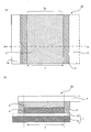
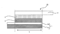
- Fig.1 (a) is a schematic diagram which shows an example of the dye-sensitized solar cell of this invention.
- FIG. 1B is a cross-sectional view taken along the line AA of the dye-sensitized solar cell of the present invention shown in FIG.
- the dye-sensitized solar cell 10 of this invention has the base material 1a and the 1st electrode layer 1b, and a dye-sensitizer is carried on the surface on the 1st electrode layer 1b.
- the dye-sensitized solar cell substrate 1 on which the porous layer 4 containing the held metal oxide semiconductor fine particles is formed and the dye-sensitized solar cell substrate 1 are arranged so as to face the electrode 1
- the insulating layer 5 is a dye. It may be formed on at least one surface of the sensitized solar cell substrate 1 or the counter electrode substrate 2.
- the insulating layer 5 is around the porous layer forming region T where the porous layer 4 is formed, and includes the dye-sensitized solar cell substrate 1 and the above-described substrate. It is formed in a region where the counter electrode substrate 2 is opposed.
- the dye-sensitized solar cell substrate 1 and the counter electrode substrate 2 are not opposed to each other around the porous layer 4 and the insulating layer 5 is formed. It is a part which is not carried out, Comprising: It has the outside part 5a which goes outside from the porous layer formation area
- FIG. 1A the base material 1a and the porous layer 4 are omitted for explanation.
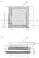
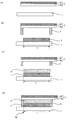
- FIG. 2 is a schematic view showing another example of the dye-sensitized solar cell of the present invention.
- FIG. 2 the case where the insulating layer 5 is formed so as to surround the porous layer forming region T will be described.
- FIG. 2 (b) is a schematic cross-sectional view taken along the line AA of the dye-sensitized solar cell of the present invention shown in FIG. 2 (a).
- the insulating layer 5 is dye-sensitized as shown in FIG.
- FIG. 2B shows an embodiment in which the insulating layer 5 is formed on the dye-sensitized solar cell substrate 1 and is not formed on the counter electrode substrate 2. May be formed on the counter electrode substrate 2 and not formed on the dye-sensitized solar cell substrate 1.
- reference numerals of members that are not described can be the same as those in FIG. 1, and thus description thereof is omitted here.
- the insulating layer in the region around the porous layer forming region where the dye-sensitized solar cell substrate and the counter electrode substrate face each other, Since the contact of the substrate can be prevented, a short circuit inside the dye-sensitized solar cell can be prevented. Further, since the electrolyte does not have fluidity by having the solid electrolyte layer, it is not necessary to seal the solid electrolyte layer with an expensive sealant having high iodine resistance. A dye-sensitized solar cell can be manufactured at low cost.
- the position of each member, the dye-sensitized solar cell substrate, and the counter electrode are used in the production of the dye-sensitized solar cell. Since high accuracy is not required for the bonding position of the base material, a dye-sensitized solar cell can be easily manufactured.
- the insulating layer is provided, when the dye-sensitized solar cell is manufactured, the bonding position of the dye-sensitized solar cell substrate and the counter electrode substrate is highly accurate. Since it is not necessary, a dye-sensitized solar cell can be easily manufactured.
- the substrate for the dye-sensitized solar cell and the counter electrode substrate when forming the dye-sensitized solar cell are provided by having the outside portion around the porous layer.
- the bonding step it is possible to discharge the air in the dye-sensitized solar cell from the outside portion and perform the bonding, so that the dye-sensitized solar cell can be easily manufactured.
- the dye-sensitized solar cell of the present invention uses a solid electrolyte layer, a multi-faced member capable of obtaining a plurality of dye-sensitized solar cells is prepared in advance and is made to a predetermined size. By cutting, a plurality of dye-sensitized solar cells can be obtained. This makes it possible to produce a large amount of dye-sensitized solar cells by manufacturing the multi-faced member by, for example, the Roll to Roll method, and cutting it into a desired size, thereby reducing the cost. Thus, it is possible to form a dye-sensitized solar cell.
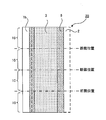
- the multi-faced member formed for mass production described above will be described with reference to the drawings.
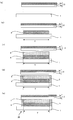
- 3 to 5 are schematic views showing examples of multi-faced members that can obtain the dye-sensitized solar cell of the present invention.
- the multi-faced member 20 used in the present invention has a plurality of dye-sensitized solar cells 10 formed in advance. By cutting this at the cutting position, the dye-sensitized solar cell 10 can be mass-produced.
- FIG. 4 when the multi-sided member shown in FIG. 4 is used, the porous layer forming region is rectangular as shown in FIG.
- Insulating layer used in the present invention is formed on at least one surface of a dye-sensitized solar cell substrate or a counter electrode substrate described later, and a porous layer described later is formed. It is formed around the porous layer forming region and in the region where the dye-sensitized solar cell substrate and the counter electrode substrate face each other.
- the dye-sensitized solar cell of the present invention has an insulating layer formed around the porous layer, which will be described later, outside the dye-sensitized solar cell from the porous layer forming region.
- the outer passage portion has an insulating portion in which the dye-sensitized solar cell substrate and the counter electrode substrate are not opposed to each other around the porous layer as described above. This refers to a portion where no layer is formed or a void portion provided in an insulating layer formed around the porous layer.
- the dye-sensitized solar cell substrate and the counter electrode substrate are not opposed around the porous layer, Since the insulating layer is formed so as to have at least one aspect of the void portion provided in the insulating layer formed around the porous layer or the insulating layer formed around the porous layer. If it exists, it will not specifically limit, The said insulating layer may be formed so that it may have the exterior part of all the aspects.
- the insulating layer used in the present invention is formed so that the dye-sensitized solar cell of the present invention has the above-described outside portion around the porous layer, and the periphery of the porous layer.
- the dye-sensitized solar cell substrate and the counter electrode substrate are formed so as not to be in electrical contact.
- the outside portion is around the porous layer, the dye-sensitized solar cell base material and the counter electrode base material are not opposed, and no insulating layer is formed.
- the insulating layer is formed so that at least one side of the porous layer forming region of the polygon is the outside portion.
- the porous layer forming region is preferably a quadrilateral, and the insulating layer is preferably formed on two opposite sides of the porous layer forming region. This is because the dye-sensitized solar cell on which the insulating layer is formed as described above can easily produce a high-quality dye-sensitized solar cell even by mass production.
- the insulating layer may be formed so as to be in close contact with the dye-sensitized solar cell substrate and the counter electrode substrate.
- the insulating layer is a dye-sensitized solar cell substrate or counter electrode group.
- a void portion not in contact with any one of the materials, or a periphery of the porous layer forming region where the porous layer is formed, and the dye-sensitized solar cell substrate and the counter electrode substrate Is not particularly limited as long as the insulating layer is formed so as to have at least one void portion of the void portion where the insulating layer is not formed in a part of the region facing each other. You may have.
- gap part in which the said insulating layer is not formed it is preferable to form the space
- the external portion as the insulating layer provided with a void portion not in contact with either the dye-sensitized solar cell substrate or the counter electrode substrate, for example, for the dye-sensitized solar cell
- an insulating layer is formed only on either the base material or the counter electrode base material, and the insulating layer is formed so as not to contact the other base material, or for example, for a dye-sensitized solar cell
- an insulating layer is formed on any surface of the base material or the counter electrode base material and the insulating layers formed on each base material are not in contact with each other can be mentioned.
- the insulating layer is formed so as to be in close contact with both sides of the dye-sensitized solar cell substrate and the counter electrode substrate. It may be.
- the dye-sensitized solar cell shown in FIGS. 1 to 5 shows a mode in which the insulating layer 5 is formed in a continuous stripe shape.
- the sensitive solar cell substrate 1 and the counter electrode substrate 2 may be formed in an island shape with an interval so as not to contact each other.
- Reference numerals not described in FIG. 6 are the same as those in FIG.
- the insulating layer is not particularly limited as long as it is formed so that the later-described dye-sensitized solar cell substrate and the counter electrode substrate are not in electrical contact with each other.
- the porous layer 4 and the solid electrolyte layer 3 may be formed on a part of the insulating layer 5, and as shown in FIG. 7B, the insulating layer 5 and the porous layer are formed. 4 and the solid electrolyte layer 3 may be formed so as to have a gap.
- FIG. 7 reference numerals not described are the same as those in FIG.
- the width of the insulating layer is not particularly limited as long as the width is such that the dye-sensitized solar cell substrate and the counter electrode substrate are not in electrical contact. As the width of such an insulating layer is wider, higher accuracy is not required at the bonding position of the dye-sensitized solar cell substrate and the counter electrode substrate, and as the width is narrower, higher accuracy is required at the bonding position. Therefore, it is preferable to determine the power generation area of the dye-sensitized solar cell and the accuracy of the bonding position. Further, specifically, the width of the insulating layer is preferably within a range of 0.5 mm to 50 mm.
- the insulating layer has an insulating property, and it is possible to form the insulating layer on either the dye-sensitized solar cell substrate or the counter electrode substrate.
- the material for the insulating layer may be transparent or may not have transparency.
- Such a material for the insulating layer may be an inorganic material or an organic material.
- the inorganic materials mention may be made of an insulating material such as SiO 2.
- organic materials include elastomers such as natural rubber and nitrile rubber, epoxy resins, acrylic resins, polyester resins, urethane resins, ionomer resins, and ethylene / acrylic acid copolymers.
- the film thickness of the insulating layer used in the present invention is not particularly limited as long as the film thickness is such that the dye-sensitized solar cell substrate and the counter electrode substrate are not in electrical contact, and will be described later. It may be thicker or thinner than the laminate of the porous layer and the solid electrolyte.
- the difference between the thickness of the insulating layer and the thickness of the laminate composed of the porous layer and the solid electrolyte layer is about ⁇ 20 ⁇ m, especially ⁇ 10 ⁇ m. It is preferable that the thickness is about ⁇ 5 ⁇ m.
- the insulating layer has adhesiveness.
- the step of bonding the dye-sensitized solar cell base material and the counter electrode base material when forming the dye-sensitized solar cell due to the adhesiveness of the insulating layer for the dye-sensitized solar cell.
- temporary bonding is performed using the insulating layer, and the dye-sensitized solar cell base material and the counter electrode base material are strengthened. It is because it becomes possible to make it adhere
- the insulating layer is in contact with either the dye-sensitized solar cell substrate or the counter electrode substrate.
- a part of a region not in contact with the other or a region where an insulating layer is not formed is included.
- the thickness of the insulating layer is, for example, Even if it is thinner or thicker than the thickness of the laminate composed of the porous layer and the solid electrolyte layer, by temporarily pressing the dye-sensitized solar cell side substrate and the counter electrode substrate, Can be bonded and firmly bonded. Therefore, even when the insulating layer has adhesiveness, the thickness of the insulating layer may be thicker or thinner than a laminate of a porous layer and a solid electrolyte layer described later. .
- the adhesiveness of the insulating layer when the dye-sensitized solar cell base material and the counter electrode base material are pressed to face each other, temporary bonding is performed using the adhesive insulating layer.
- the adhesive is not particularly limited as long as it can be used. Specifically, the adhesiveness of such an insulating layer is particularly preferably 100 mN / 25 mm or more. Moreover, the adhesiveness of the insulating layer described above is measured by using a measuring instrument such as A & D Tensilon Co., Ltd. for the force (peeling force) for peeling the respective base materials.
- the material of such an insulating layer among the above-described insulating layer materials, it is possible to use a material having adhesive properties such as a solvent type and a polymerization type. Specifically, an ultraviolet curable type, an emulsion type, Various adhesives such as hot melt type, dry lamination, heat seal, etc. can be used.
- the material of the adhesive is natural rubber, nitrile rubber, epoxy resin, vinyl acetate emulsion, acrylic, acrylate copolymer, polyvinyl alcohol, phenol resin, urethane resin, ionomer resin, etc. Various materials are mentioned.
- Solid electrolyte layer used in the present invention is formed between a dye-sensitized solar cell substrate and a counter electrode substrate, which will be described later, and is formed so as to be in contact with the porous layer. is there.
- the charges conducted between the porous layer and the counter electrode substrate, which will be described later, are transferred to the porous layer through the dye-sensitized solar cell substrate and the counter electrode substrate. It will be transported when
- the solid electrolyte layer used in the present invention does not exhibit fluidity when the dye-sensitized solar cell of the present invention is manufactured and used.
- the fluidity can be improved by adding a titanium oxide particle, a silica particle or the like to an electrolyte solution used for a general solar cell, which is obtained by solidifying a redox counter electrolyte with a polymer component.
- the polymer component in the solid electrolyte layer includes polyether, polymethacrylic acid, polyacrylic acid alkyl ester, polymethacrylic acid alkyl ester, polycaprolactone, polyhexamethylene carbonate, polysiloxane, polyethylene oxide, polypropylene oxide, polyacrylonitrile.
- Polymers having a main chain of polyvinylidene fluoride, polyvinyl fluoride, polyhexafluoropropylene, polyfluoroethylene, polyethylene, polypropylene, polyacrylonitrile or copolymers of two or more of these monomer components can be preferably used.
- a cellulose resin can be mentioned as a polymer component used for the said solid electrolyte layer. Since the cellulosic resin has high heat resistance, the electrolyte layer solidified with the cellulosic resin does not leak even at high temperatures and has high thermal stability.
- cellulose acetate such as cellulose, cellulose acetate, cellulose diacetate and cellulose triacetate, cellulose acetate butyrate (CAB), cellulose acetate propionate (CAP), cellulose acetate phthalate, cellulose such as cellulose nitrate
- cellulose ethers such as esters, methylcellulose, ethylcellulose, benzylcellulose, cyanoethylcellulose, hydroxymethylcellulose, hydroxyethylcellulose, hydroxypropylcellulose, hydroxypropylmethylcellulose, and carboxymethylcellulose. Any of these cellulose resins may be used alone, or two or more thereof may be used in combination.
- a cationic cellulose derivative is particularly preferably used from the viewpoint of compatibility with the electrolyte solution.
- the cationic cellulose derivative means a product obtained by cationization by reacting a cellulose or an OH group of the derivative with a cationizing agent.
- a solid electrolyte excellent in the retention of the electrolytic solution, and in particular, having no leakage of the electrolytic solution at a high temperature or under pressure, and excellent in thermal stability.
- the molecular weight of the cellulose resin as described above varies depending on the type of the cellulose resin and is not particularly limited.
- the weight average molecular weight is 10,000 or more ( Polystyrene conversion), and particularly preferably in the range of 100,000 to 200,000.
- a value obtained by dissolving ethyl cellulose at 2% by weight in water and measuring the viscosity at 30 ° C. is 10 mPa ⁇ s to 1000 mPa ⁇ s, particularly 5 mPa ⁇ s to The molecular weight is preferably such that the viscosity is 500 mPa ⁇ s.
- the glass transition temperature of the cellulose resin is preferably within the range of 80 ° C. to 150 ° C. in order to obtain sufficient thermal stability of the electrolyte layer.
- the content of such a polymer component is not particularly limited as long as a solid electrolyte layer can be formed. However, if the concentration of the polymer component in the solid electrolyte layer is too low, the content of the solid electrolyte layer is not limited. If the thermal stability is reduced and conversely too high, the photoelectric conversion efficiency of the solar cell is lowered. Specifically, it is preferable to contain 5 wt% to 60 wt% in the solid electrolyte layer. If the proportion of the polymer component in the solid electrolyte layer is lower than the above range, sufficient adhesion to the porous layer described later may not be obtained, and the mechanical strength of the solid electrolyte layer itself is reduced. It is not preferable because it may lead to. On the other hand, if the ratio is higher than the above range, a large amount of insulating polymer components are present, which is not preferable because the function of transporting charges may be hindered.
- the redox counter electrolyte is not particularly limited as long as it is generally used in the solid electrolyte layer.
- a combination of iodine and iodide and a combination of bromine and bromide are preferable.
- a combination of iodine and iodide a combination of metal iodide such as LiI, NaI, KI, and CaI 2 and I 2 can be mentioned.
- examples of the combination of bromine and bromide include a combination of a metal bromide such as LiBr, NaBr, KBr, and CaBr 2 and Br 2 .
- the content of the redox counter electrolyte is not particularly limited as long as the solid electrolyte layer can be formed.
- the ratio of the redox counter electrolyte to the solid electrolyte layer is 1 It is preferably within the range of 50% by weight to 50% by weight, and more preferably within the range of 5% by weight to 35% by weight. This is because when the content of the redox counter electrolyte is within the above range, a function of transporting charges from the second electrode layer to the oxide semiconductor layer can be sufficiently obtained.
- necessary components can be appropriately added in addition to the above-described polymer component and redox electrolyte.
- examples of such components include ionic liquids.
- An ionic liquid lowers the viscosity of the electrolyte and improves the conductivity of ions to improve the photoelectric conversion efficiency. Since the ionic liquid has an extremely low vapor pressure, it hardly evaporates substantially at room temperature, and there is no fear of volatilization or ignition like a general organic solvent, so that deterioration of cell characteristics due to volatilization can be prevented.
- a cation (cation) is 1-methyl-3-methylimidazolium, 1-ethyl-3-methylimidazolium, 1-propyl-3-methylimidazolium, 1-butyl-3.
- Pyridium system alicyclic amine-based, and may include those aliphatic amine.
- anion anion
- those in which the anion (anion) is an iodine ion, bromine ion, chlorine ion, tetrafluoroborate, hexafluoroborate, trifluoromethanesulfonate, trifluoroacetate, or other fluorine, cyanate, or thiocyanate Can be mentioned. Any one of these substances may be used alone, or a plurality of these substances may be mixed and used.
- an iodide ionic liquid having iodine as an anion is used, it is a supply source of iodine ions and can function as the above-described redox pair.
- the iodide ionic liquid include 1,2-dimethyl-3-n-propylimidazolium iodide, 1-methyl-3-n-propylimidazolium iodide, and 1-propyl-3- Examples thereof include methyl imidazolium iodide, 1-butyl-2,3-dimethylimidazolium iodide, and 1-hexyl-3-methylimidazolium iodide.
- redox rather than ionic liquids are used to determine the concentration of redox couples and ionic liquids in the electrolyte layer. Include as a pair.
- the ratio of the ionic liquid in the solid electrolyte layer used in the present invention varies depending on the kind of the ionic liquid, but the ratio of the redox couple / ionic liquid / resin in the solid electrolyte is 5 wt% to 60 wt%. %,
- the ionic liquid is preferably 0% by weight to 80% by weight, and the redox couple (including PMIm-I) is preferably 3% by weight to 95% by weight.
- the resin is 5% by weight to 40% by weight, and the ionic liquid is 10% by weight.
- the amount of redox couple (including PMIm-I) is preferably 10% to 85% by weight.
- the film thickness of such a solid electrolyte layer is not particularly limited as long as it is a film thickness generally employed in the solid electrolyte layer, but is in the range of 0.5 ⁇ m to 100 ⁇ m, and of these, 2 ⁇ m to 50 ⁇ m. It is preferable to be within the range.
- the porous layer used in the present invention contains metal oxide semiconductor fine particles having a dye sensitizer supported on the surface, is formed on a dye-sensitized solar cell substrate described later, and It is in contact with the solid electrolyte layer.
- the shape of the porous layer used in the present invention is not particularly limited as long as it can be formed on a dye-sensitized solar cell substrate described later, and examples thereof include a polygon. it can. Moreover, as a shape of the porous layer used for this invention, it is preferable that it is a quadrilateral among polygons. This is because the porous layer can be easily formed. Further, since the shape of the porous layer is a quadrilateral, it can be easily formed even when an insulating layer is formed around the porous layer.
- “the shape of the porous layer is a quadrilateral” means that the porous layer has a shape such as a rectangle, a parallelogram, or a rhombus.
- the “quadrangle” includes a shape in which only corners are rounded in a rectangular shape, a parallelogram shape, and a rhombus shape.
- region where the porous layer of this invention is formed it is on the base material for dye-sensitized solar cells mentioned later, Comprising: The inside of a porous layer formation area
- the porous layer may be formed so that the insulating layer described above can be formed all around the porous layer. As shown, the porous layer is formed so that there is a portion where the dye-sensitized solar cell substrate and the counter electrode substrate do not face each other and the insulating layer is not formed around the porous layer. It may be formed.
- the positional relationship between the porous layer used in the present invention and the insulating layer described above is that the porous layer forming region is not sealed by the insulating layer described above, and the insulating layer surrounds the porous layer around the porous layer.
- a porous layer may be formed inside the insulating layer described above, or FIG. As shown to a), the porous layer may be formed on the one part surface of an insulating layer.
- Metal oxide semiconductor fine particles used in the present invention are not particularly limited as long as they are made of a metal oxide having semiconductor characteristics.
- the metal oxide constituting the metal oxide semiconductor fine particles used in the present invention include TiO 2 , ZnO, SnO 2 , ITO, ZrO 2 , MgO, Al 2 O 3 , CeO 2 , Bi 2 O 3 , and Mn. 3 O 4 , Y 2 O 3 , WO 3 , Ta 2 O 5 , Nb 2 O 5 , La 2 O 3 and the like can be mentioned.
- These metal oxide semiconductor fine particles are suitable for forming a porous porous layer, and can be suitably used in the present invention because energy conversion efficiency can be improved and costs can be reduced.
- the metal oxide semiconductor fine particles used in the present invention may be all made of the same metal oxide, or two or more kinds of different metal oxides may be used.
- the metal oxide semiconductor fine particles used in the present invention may be a core-shell structure in which one type is a core fine particle and the other metal oxide semiconductor includes a core fine particle to form a shell.
- the average particle diameter of the metal oxide semiconductor fine particles used in the present invention is not particularly limited as long as the specific surface area of the porous layer is within a desired range, but is usually in the range of 1 nm to 10 ⁇ m. Is preferable, and it is particularly preferable to be within the range of 10 nm to 1000 nm. If the average particle size is smaller than the above range, the respective metal oxide semiconductor fine particles may aggregate to form secondary particles. If the average particle size is larger than the above range, the porous layer becomes thicker. This is because the porosity of the porous layer, that is, the specific surface area may be reduced. Here, when the specific surface area of the porous layer becomes small, for example, it may be difficult to carry a dye sensitizer sufficient for photoelectric conversion on the porous layer.
- the average particle size of the metal oxide semiconductor fine particles means the primary particle size.
- all the metal oxide semiconductor fine particles may have the same average particle diameter, or two or more kinds of metal oxide semiconductor fine particles having different average particle diameters may be used.
- the metal oxide semiconductor fine particles having different average particle diameters By using together the metal oxide semiconductor fine particles having different average particle diameters, the light scattering effect in the porous layer can be enhanced, and the advantage that the dye-sensitized solar cell of the present invention can be made more excellent in power generation efficiency. There is.
- examples of combinations of different average particle diameters include, for example, metal oxide semiconductor fine particles having an average particle diameter in the range of 10 nm to 50 nm.
- a combination with metal oxide semiconductor fine particles having an average particle diameter in the range of 50 nm to 800 nm can be exemplified.
- the dye sensitizer used in the present invention is not particularly limited as long as it can absorb light and generate an electromotive force.
- a dye sensitizer include organic dyes and metal complex dyes.
- the organic dyes include acridine, azo, indigo, quinone, coumarin, merocyanine, phenylxanthene, indoline, and carbazole dyes.
- a coumarin dye is preferably used.
- the metal complex dye it is preferable to use a ruthenium dye, and it is particularly preferable to use a ruthenium bipyridine dye and a ruthenium terpyridine dye which are ruthenium complexes. This is because such a ruthenium complex has a wide wavelength range of light to be absorbed, so that the wavelength range of light that can be photoelectrically converted can be greatly expanded.
- the porous layer used in the present invention may contain an optional component in addition to the metal oxide semiconductor fine particles.
- binder resin can be mentioned, for example. This is because the porous layer used in the present invention can be made less brittle by containing the binder resin in the porous layer.
- the binder resin that can be used for the porous layer is not particularly limited as long as the brittleness of the porous layer can be set to a desired level.
- a binder resin having resistance to the electrolyte layer examples include polyvinyl pyrrolidone, ethyl cellulose, caprolactan, and the like.
- binder resin used in the present invention may be only one type, or two or more types.
- the thickness of the porous layer used in the present invention can be appropriately determined according to the use of the dye-sensitized solar cell of the present invention, and is not particularly limited.
- the thickness of the porous layer in the present invention is usually preferably in the range of 1 ⁇ m to 100 ⁇ m, particularly preferably in the range of 3 ⁇ m to 30 ⁇ m. This is because if the thickness of the porous layer is larger than the above range, the porous layer itself tends to cause cohesive failure, which tends to cause membrane resistance.
- the thickness of the porous layer is thinner than the above range, it becomes difficult to form a porous layer having a uniform thickness, or the amount of the dye sensitizer carried is reduced, so that the sunlight is sufficiently absorbed. This is because there is a possibility of poor performance because it is not possible.
- the porous layer in the present invention may be composed of a single layer or may be composed of a plurality of layers laminated.
- the porous layer having a structure in which a plurality of layers are laminated any structure can be appropriately selected and employed depending on the method for producing the dye-sensitized solar cell substrate used in the present invention.
- a porous layer is formed on the oxide semiconductor layer in contact with the dye-sensitized solar cell substrate, and is formed on the oxide semiconductor layer, and is more empty than the oxide semiconductor layer.
- the aspect which is a 2 layer structure which consists of an intervening layer with a high porosity can be mentioned.
- the porous layer used in the present invention can be easily produced by a so-called transfer method. That is, the porous layer used in the present invention is prepared by a method of forming a porous layer by firing on a heat-resistant substrate and then transferring these layers onto a dye-sensitized solar cell substrate.
- the porous layer in the present invention has a two-layer structure composed of the oxide semiconductor layer and the intervening layer described above, so that the heat resistant substrate and the porous layer can be formed without degrading the performance of the porous layer. As a result, it becomes easy to produce the dye-sensitized solar cell substrate used in the present invention by the transfer method.
- the thickness ratio between the oxide semiconductor layer and the intervening layer is not particularly limited.
- the thickness of the intervening layer is preferably in the range of 10: 0.1 to 10: 5, and more preferably in the range of 10: 0.1 to 10: 3.
- the porosity of the oxide semiconductor layer is preferably in the range of 10% to 60%, and more preferably in the range of 20% to 50%. This is because if the porosity of the oxide semiconductor layer is smaller than the above range, for example, the porous layer may not be able to absorb sunlight effectively. Further, if it is larger than the above range, a desired amount of dye sensitizer may not be supported on the porous layer.
- the porosity of the intervening layer is not particularly limited as long as it is larger than the porosity of the oxide semiconductor layer. However, it is usually preferably in the range of 25% to 65%, and more preferably 30%. It is preferably in the range of ⁇ 60%.
- the porosity in this invention shows the nonoccupancy rate of the metal oxide semiconductor fine particle per unit volume.
- the porosity can be measured by a method in which the pore volume is measured with a gas adsorption amount measuring device (Autosorb-1MP; manufactured by Quantachrome) and calculated from the ratio to the volume per unit area.
- Autosorb-1MP gas adsorption amount measuring device
- Dye-sensitized solar cell substrate used in the present invention has a function as an electrode, has flexibility, and a dye-sensitized agent is carried on the surface.
- a porous layer containing metal oxide semiconductor fine particles is formed on one surface.
- the flexibility of the dye-sensitized solar cell base material is that it bends when a force of 5KN is applied in the bending test method of fine ceramics of JIS R1601 and the bending test method of metal materials of JIS Z 2248. Point to.
- a dye-sensitized solar cell substrate an embodiment having a substrate and a first electrode layer formed on the substrate (hereinafter referred to as a first embodiment), and a metal foil Two modes of the following modes (hereinafter referred to as the second mode) are conceivable. Each will be described below.
- the porous layer described above is formed on the first electrode layer.
- the base material for dye-sensitized solar cells of this aspect has a base material and the 1st electrode layer formed on the base material. Each will be described below.
- the substrate used in this embodiment is particularly limited as long as it has flexibility and has a self-supporting property that can support the first electrode layer and the porous layer used in this embodiment. Is not to be done.
- description here is abbreviate
- the base material is not particularly limited as long as it has flexibility, and specifically, a thin glass base material or resin base material can be used. Among these, a resin base material is preferable because it is lightweight, excellent in workability, and can reduce manufacturing costs.
- the substrate used in this embodiment is not particularly limited as long as the first electrode layer can be formed on the substrate, and may be a substrate having transparency.
- a base material having no transparency may be used, but a base material having transparency is preferable. This is because it is possible to form a transparent dye-sensitized solar cell substrate including a transparent substrate and a first electrode layer having transparency to sunlight.
- the resin base material examples include ethylene / tetrafluoroethylene copolymer film, biaxially stretched polyethylene terephthalate film, polyethersulfone (PES) film, polyetheretherketone (PEEK) film, and polyetherimide (PEI).
- PET polyimide
- PEN polyester naphthalate
- PC polycarbonate
- PET biaxially stretched polyethylene terephthalate film
- PEN polyester naphthalate film
- PC polycarbonate
- the thickness of the substrate used in this embodiment can be appropriately selected according to the use of the dye-sensitized solar cell, but it is usually preferably in the range of 10 ⁇ m to 2000 ⁇ m. In particular, it is preferably in the range of 50 ⁇ m to 1800 ⁇ m, more preferably in the range of 100 ⁇ m to 1500 ⁇ m.
- the base material used for this aspect is excellent in heat resistance, a weather resistance, water vapor
- oxygen permeability is 1 cc / m 2 / day ⁇ atm or less under conditions of a temperature of 23 ° C. and a humidity of 90%, and a water vapor transmission rate of 1 g under conditions of a temperature of 37.8 ° C. and a humidity of 100%.
- a substrate provided with an arbitrary gas barrier layer may be used.
- the material constituting the first electrode layer used in this embodiment is not particularly limited as long as it has a desired conductivity, and a conductive polymer material, a metal oxide, or the like can be used.
- the metal oxide is not particularly limited as long as it has desired conductivity.
- the metal oxide used in this embodiment has transparency to sunlight. Examples of such a metal oxide having transparency to sunlight include SnO 2 , ITO, IZO, and ZnO.
- any of these metal oxides can be suitably used, but among these, fluorine-doped SnO 2 (hereinafter referred to as FTO) and ITO are preferably used. This is because FTO and ITO are excellent in both conductivity and sunlight permeability.
- examples of the conductive polymer material include polythiophene, polyethylene sulfonic acid (PSS), polyaniline (PA), polypyrrole, and polyethylenedioxythiophene (PEDOT). Moreover, these can also be used in mixture of 2 or more types.
- the first electrode layer used in this embodiment may have a single layer structure or a structure in which a plurality of layers are stacked.
- Examples of the configuration in which a plurality of layers are stacked include a mode in which layers made of materials having different work functions are stacked, and a mode in which layers made of different metal oxides are stacked.
- the thickness of the 1st electrode layer used for this aspect will not be specifically limited if it exists in the range which can implement
- the thickness of the first electrode layer in this embodiment is usually preferably in the range of 5 nm to 2000 nm, and particularly preferably in the range of 10 nm to 1000 nm.
- the thickness is thicker than the above range, it may be difficult to form a uniform first electrode layer or the total light transmittance may be lowered, and it may be difficult to obtain good photoelectric conversion efficiency. This is because if the thickness is less than the above range, the conductivity of the first electrode layer may be insufficient.
- the said thickness shall point out the total thickness which totaled the thickness of all the layers, when a 1st electrode layer is comprised from a several layer.
- the method for forming the first electrode layer on the substrate can be the same as the method for forming a general electrode layer, and therefore description thereof is omitted here.
- the substrate for the dye-sensitized solar cell used in the present embodiment may be any one having at least the above-described substrate and the first electrode layer, but any other configuration as necessary. It may have.
- an auxiliary electrode formed to be in contact with the first electrode layer and made of a conductive material can be given. By forming such an auxiliary electrode, if the conductivity of the first electrode layer is insufficient, it can be supplemented. Therefore, the dye-sensitized solar cell of this aspect can be made more efficient in power generation. There is an advantage that it can be made excellent.
- the base material for dye-sensitized solar cells of this aspect consists of metal foil. Since the metal foil itself has a function as an electrode, the dye-sensitized solar cell substrate used in this embodiment does not necessarily have other configurations.
- the metal foil used as the dye-sensitized solar cell substrate is not particularly limited as long as it has flexibility, but the material is copper, aluminum, titanium, chromium, tungsten, molybdenum, platinum, tantalum. , Niobium, zirconium, zinc, various stainless steels and alloys thereof, and preferably titanium, chromium, tungsten, various stainless steels and alloys thereof.
- the thickness of the metal foil has flexibility, and the porous layer described above on the dye-sensitized solar cell substrate
- it is usually preferably within a range of 5 ⁇ m to 1000 ⁇ m, and within a range of 10 ⁇ m to 500 ⁇ m. Is more preferable, and is more preferably in the range of 20 ⁇ m to 200 ⁇ m.
- the counter electrode substrate used in the present invention is disposed so as to face the dye-sensitized solar cell substrate, has a function as an electrode, and has flexibility. Since the flexibility of the counter electrode substrate in the present invention can be equivalent to the flexibility of the dye-sensitized solar cell substrate described above, description thereof is omitted here.
- the counter electrode substrate used in the present invention is not particularly limited as long as it has a function as an electrode.
- Examples of such a counter electrode base material include those made of metal foil and those having a configuration in which a second electrode layer is formed on the counter base material.
- the second electrode layer used in the present invention may be composed of a single layer or may be composed of a plurality of layers laminated. Examples of the configuration in which a plurality of layers are laminated include an aspect in which layers made of materials having different work functions are laminated, and an aspect in which layers made of different metal oxides are laminated.
- the thickness of the second electrode layer used in the present invention is usually preferably in the range of 5 nm to 2000 nm, particularly preferably in the range of 10 nm to 1000 nm. Since the opposing base material used for this invention can use the thing similar to the base material used for the said base material for dye-sensitized solar cells, description here is abbreviate
- omitted is abbreviate
- a catalyst layer may be formed on the counter electrode base material used in the present invention, if necessary.
- the dye-sensitized solar cell of the present invention can be made more excellent in power generation efficiency.
- a catalyst layer include, for example, an embodiment in which Pt is vapor-deposited on the second electrode layer, polyethylene dioxythiophene (PEDOT), polystyrene sulfonic acid (PSS), polyaniline (PA), paratoluenesulfonic acid.
- PDOT polyethylene dioxythiophene
- PSS polystyrene sulfonic acid
- PA polyaniline
- paratoluenesulfonic acid paratoluenesulfonic acid.
- the dye-sensitized solar cell of the present invention is obtained by exciting the dye-sensitizer adsorbed on the porous layer by receiving sunlight. Work. Therefore, at least one of the dye-sensitized solar cell substrate or the counter electrode substrate needs to have transparency. Therefore, in this invention, it selects suitably so that at least one of the base material for dye-sensitized solar cells or a counter electrode base material may become a base material which has transparency.
- both the dye-sensitized solar cell substrate and the counter electrode substrate may be transparent substrates, or the dye-sensitized solar cell substrate or the counter electrode substrate. Either one may be a metal foil and the other may be a transparent substrate.
- the dye-sensitized solar cell substrate is made of a metal foil, and the counter electrode substrate is a transparent substrate. Since the dye-sensitized solar cell substrate is a metal foil, it can be directly formed on the dye-sensitized solar cell substrate by firing the porous layer. This is because the adhesion between the sensitized solar cell substrate and the porous layer can be made high. Moreover, in the dye-sensitized solar cell having the reverse structure, since light enters the porous layer through the solid electrolyte layer, there is a concern about loss of light in the solid electrolyte layer. Therefore, it is desirable to make the solid electrolyte layer thin.
- the dye-sensitized solar cell having an inverse structure is preferable because the effect of the insulating layer used in the present invention is high.
- the dye-sensitized solar cell substrate is a transparent substrate, and the counter electrode substrate is made of a metal foil.
- the dye-sensitized solar cell having such a structure can more effectively prevent a short circuit inside the dye-sensitized solar cell by having the above-described insulating layer.
- the dye-sensitized solar cell of the present invention is particularly limited as long as it has the above-described insulating layer, solid electrolyte layer, porous layer, dye-sensitized solar cell substrate, and counter electrode substrate.
- necessary members can be appropriately added.
- Such a member is disposed outside the dye-sensitized solar cell substrate and the counter electrode substrate when the dye-sensitized solar cell substrate and the counter electrode substrate are bonded to face each other. By doing so, a fixing member or the like for fixing both base materials can be mentioned.
- any member that can be fixed without causing a shift or the like in the bonding position of the bonded dye-sensitized solar cell substrate and the counter electrode substrate is used. It does not specifically limit and the fixing member used in the case of bonding of common base materials can be used.
- the material of such a fixing member low density polyethylene (LDPE), linear (linear) low density polyethylene (polymer polymerized using a multisite catalyst, LLDPE), metallocene catalyst (single site catalyst) is used.
- thermoplastic resins such as polyester resins, thermoplastic polyamide resins, and the like can be used.
- the dye-sensitized solar cell module of the present invention comprises a plurality of dye-sensitized solar cells described in the section “A. Dye-sensitized solar cell”. It is what.
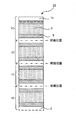
- FIG. 8 is a schematic cross-sectional view showing an example of the dye-sensitized solar cell module of the present invention.
- the dye-sensitized solar cell module 30 of the present invention includes a base material 1a and a first electrode layer 1b, and metal oxide semiconductor fine particles having a dye sensitizer supported on the surface of the first electrode layer 1b.
- a plurality of dye-sensitized solar cells 10 having a base material 1 and an insulating layer 5 formed on the surface of the counter electrode base material 2 are connected in parallel.
- a plurality of dye-sensitized solar cells may be connected in series.
- dye-sensitized solar cell used in the present invention can be the same as that described in the section “A. Dye-sensitized solar cell”, description thereof is omitted here.
- a mode in which a plurality of dye-sensitized solar cells are connected is particularly limited as long as a desired electromotive force can be obtained by the dye-sensitized solar cell module of the present invention. is not.
- Such an embodiment may be an embodiment in which individual dye-sensitized solar cells are connected in series, or may be connected in parallel.
- the manufacturing method of the dye-sensitized solar cell of the present invention is a metal having a function as an electrode, having flexibility, and having a dye-sensitizing agent supported on the surface.
- a porous layer containing oxide semiconductor fine particles is disposed on one surface so as to face the dye-sensitized solar cell substrate and the dye-sensitized solar cell substrate.
- the dye A porous layer forming step for forming the porous layer on a substrate for sensitized solar cells, a solid electrolyte layer forming step for forming a solid electrolyte layer so as to be in contact with the porous layer, and the dye sensitization Type solar cell substrate or the above counter electrode group At least one surface of the material, around the region corresponding to the porous layer forming region where the porous layer is formed, and pasting the dye-sensitized solar cell substrate and the counter electrode substrate
- the steps of forming an insulating layer in the region where the dye-sensitized solar cell substrate and the counter electrode substrate face each other are performed in random order, and then the dye-sensitized And a bonding step in which the substrate for a solar cell and the counter electrode substrate are bonded to each other so as to sandwich the porous layer and the electrolyte
- the porous layer forming step, the solid electrolyte layer forming step, and the insulating layer forming step can be performed in any order. Therefore, it is possible to adjust the order of the above steps according to the shape of the dye-sensitized solar cell to be manufactured.
- the manufacturing method of the dye-sensitized solar cell of this invention is demonstrated using figures.
- FIG. 9 is a process diagram showing an example of the method for producing the dye-sensitized solar cell of the present invention.
- the method for producing a dye-sensitized solar cell of the present invention is opposed to the dye-sensitized solar cell substrate 1 made of a metal foil and the dye-sensitized solar cell substrate 1.
- the counter electrode substrate 2 having the counter substrate 2a and the second electrode layer 2b is prepared (FIG. 9A), and then the surface of the dye-sensitized solar cell substrate 1 is prepared.
- a porous layer forming step (FIG.
- FIG. 10 is a process diagram showing another example of the method for producing the dye-sensitized solar cell of the present invention.
- the method for producing a dye-sensitized solar cell of the present invention faces the dye-sensitized solar cell substrate 1 made of a metal foil and the dye-sensitized solar cell substrate 1.
- the counter electrode substrate 2 having the counter substrate 2a and the second electrode layer 2b prepared (FIG.
- a solid electrolyte layer forming step for forming the solid electrolyte layer 3 on the porous layer 4 (FIG. 10C), the dye-sensitized solar cell substrate 1, and the counter electrode substrate 2
- an insulating layer may be formed on the dye-sensitized solar cell substrate before the porous formation step and the solid electrolyte formation step.
- 9 and 10 exemplify the case where a metal foil is used as the dye-sensitized solar cell base material
- the dye-sensitized solar cell base material includes You may use the base material for dye-sensitized solar cells which has the 1st electrode layer formed in this.
- the counter electrode substrate may be made of a metal foil, or the counter electrode having the counter substrate and the second electrode layer. A substrate may be used.
- the present invention since the solid electrolyte layer and the insulating layer are formed by the solid electrolyte layer forming step and the insulating layer forming step, the substrate is opposed to the dye-sensitized solar cell substrate in the bonding step. Since high accuracy is not required at the bonding position when the electrode substrate is bonded, a dye-sensitized solar cell can be easily manufactured.
- the dye-sensitized solar cell substrate and the counter electrode substrate on which the porous layer is formed are sealed with the sealing agent.
- a dye-sensitized solar cell can be easily manufactured as compared with a conventional method for manufacturing a dye-sensitized solar cell in which an electrolyte is injected to form an electrolyte layer.
- the dye-sensitized solar cell substrate, the counter electrode substrate, and the combination of the dye-sensitized solar cell substrate and the counter electrode substrate used in the present invention are described in “A. Dye-sensitized solar cell”. Since it can be the same as that described in the section of “Battery”, the description is omitted here.
- porous layer forming step the solid electrolyte layer forming step, the insulating layer forming step, and the bonding step in the present invention will be described.
- Porous layer forming step This step is a step of forming the porous layer on the dye-sensitized solar cell substrate.
- the method for forming the porous layer used in this step is not particularly limited as long as it can form a desired porous layer on the dye-sensitized solar cell substrate.
- a metal foil is used as the substrate for the dye-sensitized solar cell, and the porous layer is baked and formed on the metal foil (hereinafter referred to as a third aspect).
- a method for forming a porous layer by applying a porous layer forming composition for forming a porous layer on the dye-sensitized solar cell substrate in a pattern hereinafter referred to as a fourth embodiment).
- the formation method of the porous layer of this aspect uses a metal foil as said base material for dye-sensitized solar cells, forms the said porous layer by baking on the said metal foil. Is the method.
- the metal foil used in this embodiment is not particularly limited as long as it has heat resistance that can withstand the firing temperature when firing the porous layer. Moreover, in this aspect, since a metal foil is used as the base material for the dye-sensitized solar cell, a transparent base material is prepared as the counter electrode base material.
- the metal foil has a high heat-resistant temperature, the metal foil has an advantage that the range of selection of materials used for the porous layer is widened and the adhesion between the metal foil and the porous layer is good.
- porous layer forming method of this embodiment first, a porous layer forming coating solution comprising metal oxide semiconductor fine particles, a binder resin, and a solvent is prepared. Next, the porous layer forming coating solution prepared on the metal foil is applied in a desired thickness to form a porous layer forming coating film, and the porous layer forming coating film is fired. A porous layer forming layer is formed by thermally decomposing the binder resin. Next, a porous layer is formed by attaching a dye sensitizer to the surface of the porous layer forming layer.
- metal oxide semiconductor fine particles used in this embodiment can be the same as those described in the section “A. Dye-sensitized solar cell”, description thereof is omitted here.
- the binder resin used for the porous layer forming coating solution is not particularly limited as long as it is thermally decomposed by firing.
- binder resins include cellulose resins, polyester resins, polyamide resins, polyacrylate resins, polyacryl resins, polycarbonate resins, polyurethane resins, polyolefin resins, polyvinyl acetal resins, fluorine
- polyhydric alcohols such as polyethylene glycol can be used.
- the solvent used in the porous layer forming coating solution is not particularly limited as long as it can dissolve or disperse the binder resin in a desired amount.
- a solvent include water and various solvents such as methanol, ethanol, isopropyl alcohol, propylene glycol monomethyl ether, terpineol, dichloromethane, acetone, acetonitrile, ethyl acetate, and tert-butyl alcohol.
- the method for applying the coating liquid for forming a porous layer is not particularly limited as long as the coating liquid for forming a porous layer can be uniformly applied in a pattern with a desired film thickness on a metal foil.
- it can be the same as a general coating method.
- a general application method for example, die coating, gravure coating, gravure reverse coating, roll coating, reverse roll coating, bar coating, blade coating, knife coating, air knife coating, slot die coating, slide die coating, dip coating, Examples thereof include micro bar coating, micro bar reverse coating, offset coating, and screen printing (rotary method).
- the thickness of the coating film for forming a porous layer formed on the metal foil is not particularly limited as long as it can form a porous layer having a desired thickness. However, it is preferably in the range of 0.5 ⁇ m to 50 ⁇ m, in particular in the range of 2 ⁇ m to 30 ⁇ m, particularly in the range of 5 ⁇ m to 20 ⁇ m. This is because when the thickness of the coating film for forming the porous layer is less than the above range or exceeds the above range, it is difficult to form the porous layer with a desired thickness.
- the porous layer forming coating film may be pressurized before firing the porous layer forming coating film. This is because pressurization of the porous layer-forming coating film can improve the adhesion between the formed porous layer and the dye-sensitized solar cell substrate.
- the method for pressurizing the coating film for forming the porous layer can be the same as that used in the production of a general dye-sensitized solar cell, and thus description thereof is omitted here.
- the method for firing the coating film for forming the porous layer in this embodiment is not particularly limited as long as it can be uniformly fired without heating unevenness, and a known firing method can be used.
- the firing temperature in this embodiment is not particularly limited as long as it is a temperature at which the binder resin contained in the coating film for forming a porous layer can be thermally decomposed, and is appropriately determined according to the thermal decomposition temperature of the binder resin. It is something that can be done. In particular, it is preferably in the range of 250 ° C. to 550 ° C., in particular in the range of 350 ° C. to 550 ° C., particularly in the range of 400 ° C. to 550 ° C.
- the porous layer formed by the porous layer forming method of this embodiment is used for a dye-sensitized solar cell.
- the dye sensitizer is not particularly limited as long as the dye sensitizer can receive sunlight, and a method used in manufacturing a general dye-sensitized solar cell; The same can be said.
- dye sensitizer used in this embodiment can be the same as that described in the section “A. Dye-sensitized solar cell”, description thereof is omitted here.
- the method for forming a porous layer of this aspect is to apply the porous layer forming composition for forming a porous layer in a pattern on the dye-sensitized solar cell substrate.
- This is a method for forming a porous layer.
- heat treatment (hereinafter sometimes simply referred to as heat treatment) may be performed at a temperature lower than the heat resistant temperature of the dye-sensitized solar cell substrate.
- the dye-sensitized solar cell substrate used in this embodiment may be composed of a metal foil, or may be composed of a substrate and a first electrode layer formed on the substrate. .
- the substrate include a thin glass substrate and a resin film.
- the counter electrode substrate may be prepared as a substrate in which at least one of the dye-sensitized solar cell substrate and the counter electrode substrate has transparency.
- a porous layer forming layer is formed by applying and drying a porous layer forming composition containing metal oxide semiconductor fine particles and a solvent, and then forming a porous layer.
- a porous layer is formed by attaching a dye sensitizer to the layer for forming a quality layer.
- the metal oxide semiconductor fine particles used in the porous layer forming composition can be the same as those described in the section of “A. Dye-sensitized solar cell”, and thus description thereof is omitted. To do.
- the solvent is not particularly limited as long as the metal oxide semiconductor fine particles can be dispersed, the resin component can be dissolved or dispersed, and can be removed by natural drying or heat treatment.
- a solvent include, but are not limited to, water, ethanol, isopropyl alcohol, ethyl acetate, methyl ethyl ketone, cyclohexanone, toluene, xylene, and the like. Two or more kinds of solvents may be mixed and used. It is more desirable to use water or an alcohol-based solvent from the viewpoint of the influence of volatile components after film formation on the environment.
- the coating method of the porous layer forming composition and the film thickness of the coating film of the porous layer forming composition it is uniformly formed with a desired film thickness on the dye-sensitized solar cell substrate. It is not particularly limited as long as it is possible, and the coating method for the porous layer forming coating liquid and the film thickness of the porous layer forming coating film described in the section “(1) Third aspect” The description is omitted here.
- the dye sensitizer in this embodiment and the method of attaching the dye sensitizer to the porous layer forming layer can be the same as the method described in the section “(1) Third embodiment”. Therefore, the description here is omitted.
- the method for forming a porous layer of this aspect is that the porous layer is baked and formed on a heat resistant substrate, and then the porous layer is disposed on the dye-sensitized solar cell substrate. Next, the porous layer is formed by peeling the heat-resistant substrate (transfer method).
- the method for forming a porous layer of the present embodiment is particularly limited as long as the porous layer is formed by baking on a heat-resistant substrate and can be disposed on the dye-sensitized solar cell substrate.
- the porous layer is formed by baking on a heat-resistant substrate and can be disposed on the dye-sensitized solar cell substrate.
- the dye-sensitized solar cell base material used in this embodiment is preferably composed of a base material and a first electrode layer formed on the base material.
- a counter electrode base material used for this aspect what is necessary is just to prepare at least one of the said dye-sensitized solar cell base material or a counter electrode base material as a base material which has transparency.
- the heat-resistant substrate used in this embodiment is not particularly limited as long as it has desired heat resistance.
- a porous layer is formed on the heat-resistant substrate, a high-temperature baking process is generally performed. Therefore, as the heat-resistant substrate used in the present invention, the porous layer is formed when the porous layer is formed. What has the heat resistance which can endure the heating temperature at the time of the baking process to be called is preferable. Since such a heat-resistant substrate can be the same as that used in the production of a general dye-sensitized solar cell, description thereof is omitted here.
- the method for forming the porous layer on the heat-resistant substrate can be the same as the method used in forming the porous layer on the metal foil in “(1) Third aspect”. Therefore, the description here is omitted.
- the method for forming the first electrode layer on the porous layer is not particularly limited as long as the first electrode layer can be uniformly formed with a desired film thickness on the porous layer.
- the material and the like of the first electrode layer used in this embodiment can be the same as those described in the section “A. Dye-sensitized solar cell”, and thus description thereof is omitted here.
- the method for adhering the base material on the first electrode layer is not particularly limited as long as it can adhere the base material and the first electrode layer with a desired adhesive force.
- a method of bonding the base material and the first electrode layer through an adhesive layer is used.
- the adhesive layer can be the same as that used in the production of a general dye-sensitized solar cell, description thereof is omitted here.
- the heat-resistant substrate peeling method is not particularly limited as long as the heat-resistant substrate can be peeled without damaging the porous layer, and a general peeling method can be used.
- the heat-resistant substrate can be peeled off by mechanical polishing or chemical removal such as etching.
- a porous layer may be formed in a part of the insulating layer.
- the insulating layer described later is formed so that the dye-sensitized solar cell substrate and the counter electrode substrate are not in electrical contact in the dye-sensitized solar cell manufactured by the manufacturing method of the present invention. If there is no particular limitation. Therefore, since it is not necessary to form the porous layer with high positional accuracy on the porous formation region where the insulating layer is not formed, the porous layer can be easily formed.
- Solid electrolyte layer forming step This step is a step of forming a solid electrolyte layer so as to be in contact with the porous layer.
- the method for forming the solid electrolyte layer is not particularly limited as long as the solid electrolyte layer can be formed on the porous layer so as to be in contact with the porous layer with a desired film thickness.
- a composition for forming a solid electrolyte layer in which additives such as a polymer component, a redox counter electrolyte, a crosslinking agent, and a photopolymerization initiator are dispersed or dissolved in an appropriate solvent is prepared, and the solid electrolyte is prepared.
- Solid electrolyte layer by applying the solid electrolyte layer forming composition in a pattern on the porous layer.
- Solid electrolyte layer can be easily formed by injecting a solid electrolyte layer material after sealing the dye-sensitized solar cell substrate and the counter electrode substrate with a sealant or the like, and then forming a solid electrolyte layer. It is because it becomes possible to form.
- the polymer component and the redox counter electrolyte can be the same as those described in the section “A. Dye-sensitized solar cell”, description thereof is omitted here.
- other components used in the composition for forming a solid electrolyte layer can be the same as those used when forming a general solid electrolyte layer, and thus description thereof is omitted here.
- the solid electrolyte layer can be the same as that described in the above-mentioned section “A. Dye-sensitized solar cell”, and the description thereof is omitted here.
- Insulating layer forming step This step is performed in a region corresponding to the porous layer forming region where the porous layer is formed on at least one surface of the dye-sensitized solar cell substrate or the counter electrode substrate.
- An insulating layer is provided in a region where the dye-sensitized solar cell substrate and the counter electrode substrate face each other when the dye-sensitized solar cell substrate and the counter electrode substrate are bonded to each other. Is a step of forming.
- the insulating layer is formed by forming the insulating layer so that the dye-sensitized solar cell formed by the method for manufacturing a dye-sensitized solar cell of the present invention does not cause an internal short circuit. If it can, it will not specifically limit.
- a method for forming the insulating layer for example, an insulating layer forming composition for forming an insulating layer is applied in a pattern to at least one of the dye-sensitized solar cell substrate or the counter electrode substrate.
- Method for forming insulating layer Method for forming insulating layer, method for forming insulating layer by attaching to at least one of base material for dye-sensitized solar cell or counter electrode base material using insulating tape, porous layer and solid
- the dye-sensitized solar cell substrate on which the electrolyte layer is formed and the counter electrode substrate are opposed to each other so as to sandwich the porous layer and the solid electrolyte layer, and the dye-sensitized solar cell substrate and the counter electrode
- a method of forming an insulating layer by sandwiching and pressing an insulating layer material (polymer film or the like) between substrates, and at least one of the dye-sensitized solar cell substrate and the counter electrode substrate Examples thereof include a method of forming an insulating layer by forming an insulating vapor deposition film such as 2 by vapor deposition, sputtering, CVD, or the like.
- the insulating layer forming composition for forming the insulating layer is applied in a pattern to at least one of the dye-sensitized solar cell substrate or the counter electrode substrate, or has an insulating property.
- the insulating layer is preferably formed by using a tape. This is because the insulating layer can be easily formed.
- the composition for forming an insulating layer contains the material of the insulating layer described in the section “A. Dye-sensitized solar cell”.
- the tape having the above-described insulating property is “A. Dye”. It includes the material of the insulating layer described in the section “sensitized solar cell” and has a desired width and thickness of the insulating layer.
- the insulating material (polymer film) includes the material of the insulating layer described in the section “A. Dye-sensitized solar cell” and has heat sealability, and heat sealability. It does not have, or includes the material of the insulating layer described in the section “A. Dye-sensitized solar cell”, and includes both those having adhesiveness and those having no adhesiveness.
- a method of applying the insulating layer forming composition in a pattern it can be the same as a general pattern application method, and in particular, a printing method, an ink jet method, a dispenser method, a die coat, a gravure coat, a gravure reverse coat, Offset coating and screen printing (rotary method) are preferred.
- any method can be used as long as the tape can be applied to a predetermined position of the dye-sensitized solar cell substrate or the counter electrode substrate. Since it is not limited and can be the same as a general method of attaching a tape, description thereof is omitted here.
- the insulating layer formed in this step is insulated so that the dye-sensitized solar cell to be produced is not in electrical contact with the substrate for the dye-sensitized solar cell and the counter electrode substrate around the porous layer. If it is a layer, it will not specifically limit.
- the insulating layer formed in this step among the dye-sensitized solar cells to be manufactured, the outside is externally connected to the outside of the dye-sensitized solar cell from the porous layer forming region where the porous layer is formed. It is more preferable that it is formed so as to have an outer passage portion.
- the air in the dye-sensitized solar cell can be discharged from the outside portion, and the dye-sensitized solar cell substrate and the counter electrode substrate can be bonded together. This is because a solar cell can be easily formed.
- the above-described outside portion can be the same as that described in the section “A. Dye-sensitized solar cell”, and thus description thereof is omitted here.
- the insulating layer may be formed continuously, or as shown in FIG. 6, the insulating layer is manufactured by the method for manufacturing the dye-sensitized solar cell of the present invention.
- the dye-sensitized solar cell may be formed in an island shape with an interval that does not cause an internal short circuit.
- Bonding Step is a step of bonding the dye-sensitized solar cell base material and the counter electrode base material facing each other so as to sandwich the porous layer and the electrolyte layer.
- the dye-sensitized solar cell substrate and the counter electrode substrate are combined with the porous layer and the solid layer. Since the electrolyte layers are bonded so as to sandwich each other, they can be manufactured in one manufacturing line, and the manufacturing efficiency can be improved.
- the dye-sensitized solar cell substrate and the counter electrode substrate used in this step are combined with the porous layer and the solid.
- the method is not particularly limited as long as the electrolyte layers can be bonded to each other so as to sandwich the electrolyte layer, and can be the same as the method used in a general method for manufacturing a dye-sensitized solar cell.
- the method for producing the dye-sensitized solar cell of the present invention is not particularly limited as long as it is a production method having the bonding step, and necessary steps can be appropriately added.
- Examples of such a process include a process of cutting the dye-sensitized solar cell assembled in the above-described bonding process into a desired size.
- the electrolyte since the electrolyte is solid, the assembled dye-sensitized solar cell can be cut to a desired size.
- the catalyst layer process etc. which form a catalyst layer on the said counter electrode base material are mentioned.
- the formation method of the said catalyst layer since it can be made to be the same as that of the method used in the case of manufacture of a general dye-sensitized solar cell, description here is abbreviate
- the porous layer forming composition for forming a porous layer is applied in a pattern to the dye-sensitized solar cell substrate.
- a solid electrolyte layer is formed by applying a solid electrolyte layer forming composition that forms a solid electrolyte layer on the porous layer in a pattern, and the insulating layer
- the insulating layer is formed by applying the insulating layer forming composition for forming the insulating layer in a pattern on at least one of the dye-sensitized solar cell substrate or the counter electrode substrate. It is preferable.
- the dye-sensitized solar cell of the present invention can be manufactured on one manufacturing line, and the manufacturing efficiency can be improved.
- both the dye-sensitized solar cell substrate and the counter electrode substrate used in the present invention have flexibility, the above-described members can be obtained by performing all the above steps by a coating method. Compared with the case of using a tape or the like, the load applied to the dye-sensitized solar cell substrate and the counter electrode substrate is small, and it is possible to prevent the processing accuracy from being lowered.
- a dye-sensitized solar cell using a multi-faced member formed with a plurality of dye-sensitized solar cells as shown in FIGS. 3 to 5 is used. It is also possible to mass produce batteries.
- a method for producing a dye-sensitized solar cell using such a multifaceted member first, in the above-described porous layer forming step, solid electrolyte layer forming step, and insulating layer forming step, a plurality of dye-sensitized types A plurality of members necessary for the solar cell are formed, and then, in the bonding step described above, the dye-sensitized solar cell base material and the counter electrode base material on which the respective members are formed are bonded to each other.
- An example is a method of forming a multi-sided member on which the dye-sensitized solar cell is formed, and cutting the member at a predetermined cutting position.
- the porous layer forming step, the solid electrolyte layer forming step, and the insulating layer forming step used in the method for producing a plurality of dye-sensitized solar cells when forming the multi-faced member described above a plurality of desired dye sensitizing methods are used.
- a plurality of desired dye sensitizing methods are used.
- the bonding step it is possible to improve the production efficiency from being able to manufacture the multi-faceted member in one production line, compared to the case where each member is formed using a tape or the like, It is possible to prevent a reduction in processing accuracy.
- the multi-sided member can be formed by using a Roll to Roll method or the like, and by cutting the member, a dye-sensitized solar cell can be mass-produced. A battery can be formed.
- the present invention is not limited to the above embodiment.
- the above-described embodiment is an exemplification, and the technical idea described in the claims of the present invention has substantially the same configuration and exhibits the same function and effect regardless of the case. It is included in the technical scope of the invention.
- Example 1 A titanium foil is prepared as a dye-sensitized solar cell substrate, a transparent conductive film having an ITO film formed on a PEN film is prepared as a counter substrate, and platinum is formed on the ITO film with a thickness of 13 mm (transmittance 72). %) To prepare a counter electrode base material.
- a porous layer-forming coating solution was prepared by adding 5% of ethyl cellulose (ST-100, manufactured by Nisshin Kasei Co., Ltd.) as a polymer component to a dispersion obtained by dispersing P25 manufactured by Nippon Aerosil Co., Ltd. in ethanol.
- the porous layer forming coating solution was applied on a titanium foil with a doctor blade in an area of 10 mm ⁇ 10 mm and dried at 120 ° C. to obtain a porous layer forming coating film having a thickness of 6 ⁇ m.
- a pressure of 0.1 t / cm was applied to the coating film for forming the porous layer with a press.
- the reason why the polymer component is added at the time of pressing is to prevent the coating film for forming the porous layer from being taken on the roll. After the pressing, it was fired at 500 ° C. to obtain a porous layer forming layer. Next, the porous layer forming layer described above was dissolved in a dye solution in which a ruthenium complex (RuL 2 (NCS) 2 manufactured by Solaronix) was dissolved in absolute ethanol to a concentration of 3.0 ⁇ 10 ⁇ 4 mol / l. Was immersed for 20 hours. After immersion, the dye solution pulled up from the dye solution and adhered to the porous layer was washed with acetonitrile and air-dried. As a result, a porous layer carrying a dye sensitizer was obtained.
- a ruthenium complex RuL 2 (NCS) 2 manufactured by Solaronix
- Solid electrolyte layer forming process 10.0 g of PMIm-I and 0.24 g of I 2 were added to 3.64 g of EMIm-B (CN) 4, and the resulting mixture was expanded and dissolved. Further, 28 g of a methanolic 5 w% solution of cationic hydroxycellulose (Daicel Chemical Co., Ltd., Gelner QH-200) was added to this solution and stirred to prepare a coating composition for forming a solid electrolyte layer. Next, the above-mentioned composition for forming a solid electrolyte layer is applied with a doctor blade to the same region where the porous layer of the dye-sensitized solar cell substrate is formed, and dried at 100 ° C. Thus, the solid electrolyte layer was provided with a thickness of 4 ⁇ m.
- Example 2 In the insulating layer forming step, a dye-sensitized solar cell was obtained in the same manner as in Example 1 except that a double-sided tape having a thickness of 15 ⁇ m (400P15 manufactured by Kyori Giken Chemical Co., Ltd.) was used.
- Example 3 A dye-sensitized solar cell was obtained in the same manner as in Example 1 except that the area of the dye-sensitized solar cell substrate was 10 mm ⁇ 40 mm and an insulating layer was sandwiched between the insulating layers 5 in FIG. It was. Next, as shown in FIG. 3, a 10 mm ⁇ 10 mm dye-sensitized solar cell was obtained by cutting at a cutting position on the insulating layer.
- Example 4 A porous layer is formed on a 30 mm ⁇ 30 mm titanium foil by pattern coating the porous layer forming coating solution at four locations in an area of 10 mm ⁇ 10 mm, and insulated at the position of the insulating layer 5 in FIG.
- a dye-sensitized solar cell was obtained in the same manner as in Example 1 except that the layer was sandwiched.
- FIG. 5 a 10 mm ⁇ 10 mm dye-sensitized solar cell was obtained by cutting at a cutting position on the insulating layer.
- Example 5 As a dye-sensitized solar cell substrate, a transparent conductive film having an ITO film formed on a PEN film was prepared, and the area was 10 mm ⁇ 40 mm. Moreover, the counter electrode base material was prepared by laminating
- the porous layer forming layer described above was dissolved in a dye solution in which a ruthenium complex (RuL 2 (NCS) 2 manufactured by Solaronix) was dissolved in absolute ethanol to a concentration of 3.0 ⁇ 10 ⁇ 4 mol / l. was immersed for 20 hours. After immersion, the dye solution pulled up from the dye solution and adhered to the porous layer was washed with acetonitrile and air-dried. As a result, a porous layer carrying a dye sensitizer was obtained.
- a ruthenium complex RuL 2 (NCS) 2 manufactured by Solaronix
- the above-mentioned composition for forming a solid electrolyte layer is applied with a doctor blade to the same region where the porous layer of the dye-sensitized solar cell substrate is formed, and dried at 100 ° C.
- the solid electrolyte layer was provided with a thickness of 4 ⁇ m.
- the dye-sensitized solar cell substrate and the counter electrode substrate were stacked and adhered. Then, it aged at 50 degreeC for 7 days. Next, a 10 mm ⁇ 10 mm dye-sensitized solar cell was obtained by cutting at the cutting position shown in FIG.
- SYMBOLS 1 Base material for dye-sensitized solar cells 1a ... Base material 1b ... 1st electrode layer 2 ... Counter electrode base material 2a ... Counter base material 2b ... 2nd electrode layer 3 ... Solid electrolyte layer 4 ... Porous layer 5 ... Insulating layer 10 . Dye-sensitized solar cell 20 ... Multi-sided member 30 ... Dye-sensitized solar cell module
Landscapes
- Engineering & Computer Science (AREA)
- Power Engineering (AREA)
- Microelectronics & Electronic Packaging (AREA)
- Chemical & Material Sciences (AREA)
- Chemical Kinetics & Catalysis (AREA)
- Electrochemistry (AREA)
- Materials Engineering (AREA)
- Photovoltaic Devices (AREA)
- Hybrid Cells (AREA)
Priority Applications (3)
| Application Number | Priority Date | Filing Date | Title |
|---|---|---|---|
| CN201080038646.9A CN102484302B (zh) | 2009-11-16 | 2010-07-06 | 色素敏化型太阳能电池 |
| US13/389,887 US9064637B2 (en) | 2009-11-16 | 2010-07-06 | Dye-sensitized solar cell |
| US14/695,549 US20150235774A1 (en) | 2009-11-16 | 2015-04-24 | Dye-sensitized solar cell |
Applications Claiming Priority (2)
| Application Number | Priority Date | Filing Date | Title |
|---|---|---|---|
| JP2009261158A JP4868058B2 (ja) | 2009-11-16 | 2009-11-16 | 色素増感型太陽電池 |
| JP2009-261158 | 2009-11-16 |
Related Child Applications (2)
| Application Number | Title | Priority Date | Filing Date |
|---|---|---|---|
| US13/389,887 A-371-Of-International US9064637B2 (en) | 2009-11-16 | 2010-07-06 | Dye-sensitized solar cell |
| US14/695,549 Division US20150235774A1 (en) | 2009-11-16 | 2015-04-24 | Dye-sensitized solar cell |
Publications (1)
| Publication Number | Publication Date |
|---|---|
| WO2011058786A1 true WO2011058786A1 (ja) | 2011-05-19 |
Family
ID=43991450
Family Applications (1)
| Application Number | Title | Priority Date | Filing Date |
|---|---|---|---|
| PCT/JP2010/061488 Ceased WO2011058786A1 (ja) | 2009-11-16 | 2010-07-06 | 色素増感型太陽電池 |
Country Status (4)
| Country | Link |
|---|---|
| US (2) | US9064637B2 (enExample) |
| JP (1) | JP4868058B2 (enExample) |
| CN (1) | CN102484302B (enExample) |
| WO (1) | WO2011058786A1 (enExample) |
Cited By (1)
| Publication number | Priority date | Publication date | Assignee | Title |
|---|---|---|---|---|
| JP2014049426A (ja) * | 2012-09-04 | 2014-03-17 | Dainippon Printing Co Ltd | 有機系太陽電池素子モジュールの製造方法 |
Families Citing this family (3)
| Publication number | Priority date | Publication date | Assignee | Title |
|---|---|---|---|---|
| KR20130006561A (ko) * | 2011-07-08 | 2013-01-17 | 현대자동차주식회사 | 다공성 필름형 고체 전해질 및 이를 이용한 염료감응 태양전지와 이의 제조방법 |
| KR20130020184A (ko) * | 2011-08-19 | 2013-02-27 | 한국전자통신연구원 | 염료 감응 태양 전지 및 전해질의 제조 방법 |
| WO2013171520A1 (en) | 2012-05-18 | 2013-11-21 | Isis Innovation Limited | Optoelectronic device comprising perovskites |
Citations (5)
| Publication number | Priority date | Publication date | Assignee | Title |
|---|---|---|---|---|
| JP2006286534A (ja) * | 2005-04-04 | 2006-10-19 | Nippon Oil Corp | フレキシブル色素増感太陽電池 |
| JP2007265776A (ja) * | 2006-03-28 | 2007-10-11 | Nippon Oil Corp | フレキシブル色素増感型太陽電池 |
| JP2008176993A (ja) * | 2007-01-17 | 2008-07-31 | Kyocera Corp | 光電変換装置及びその製造方法並びに光発電装置 |
| WO2009057704A1 (ja) * | 2007-11-02 | 2009-05-07 | Nippon Kayaku Kabushiki Kaisha | 色素増感太陽電池モジュール |
| JP2009238571A (ja) * | 2008-03-27 | 2009-10-15 | Dainippon Printing Co Ltd | 色素増感型太陽電池用電解質 |
Family Cites Families (21)
| Publication number | Priority date | Publication date | Assignee | Title |
|---|---|---|---|---|
| US20050268962A1 (en) * | 2000-04-27 | 2005-12-08 | Russell Gaudiana | Flexible Photovoltaic cells, systems and methods |
| US20050257827A1 (en) * | 2000-04-27 | 2005-11-24 | Russell Gaudiana | Rotational photovoltaic cells, systems and methods |
| US7022910B2 (en) * | 2002-03-29 | 2006-04-04 | Konarka Technologies, Inc. | Photovoltaic cells utilizing mesh electrodes |
| JP2002368233A (ja) * | 2001-06-07 | 2002-12-20 | Nippon Kayaku Co Ltd | 光電変換素子 |
| US7202412B2 (en) * | 2002-01-18 | 2007-04-10 | Sharp Kabushiki Kaisha | Photovoltaic cell including porous semiconductor layer, method of manufacturing the same and solar cell |
| JP4465971B2 (ja) | 2003-03-26 | 2010-05-26 | 株式会社ブリヂストン | 色素増感型太陽電池用対向電極及び色素増感型太陽電池 |
| EP2204875B8 (en) * | 2003-05-30 | 2012-03-14 | Fujikura Ltd. | Electrolyte composition and photoelectric conversion element using same |
| EP1560272B1 (en) * | 2004-01-29 | 2016-04-27 | Panasonic Intellectual Property Management Co., Ltd. | Solar cell module |
| JP2005243388A (ja) | 2004-02-26 | 2005-09-08 | Mitsubishi Paper Mills Ltd | 色素増感型太陽電池 |
| JP2005251605A (ja) | 2004-03-05 | 2005-09-15 | Toppan Printing Co Ltd | 色素増感太陽電池およびモジュールおよび色素増感太陽電池の製造方法 |
| EP1624472A3 (en) * | 2004-07-08 | 2011-03-16 | Sumitomo Chemical Company, Limited | Porous Electrodes, Devices including the Porous Electrodes, and Methods for their Production |
| US8018638B2 (en) * | 2004-07-20 | 2011-09-13 | Ajjer Llc | Fabrication of cell cavities for electrooptic devices |
| JP2006331791A (ja) | 2005-05-25 | 2006-12-07 | Bridgestone Corp | 色素増感型太陽電池用セパレータ及びその利用 |
| DE112006002294T5 (de) * | 2005-09-02 | 2008-10-30 | Kyocera Corp. | Lichtelektrische Umwandlungsvorrichtung und Verfahren zu deren Herstellung sowie lichtelektrische Energieerzeugungsvorrichtung |
| US20090293947A1 (en) * | 2005-10-11 | 2009-12-03 | Kyocera Corporation | Photoelectric Conversion Device and Method of Manufacturing the Same, and Photoelectric Power Generation Device |
| KR100869802B1 (ko) * | 2006-11-17 | 2008-11-21 | 삼성에스디아이 주식회사 | 염료감응 태양전지용 전해질, 이를 포함하는 염료감응태양전지, 및 이의 제조방법 |
| JP5089157B2 (ja) * | 2006-12-15 | 2012-12-05 | 新光電気工業株式会社 | 色素増感型太陽電池モジュールおよびその製造方法 |
| WO2008093126A1 (en) * | 2007-02-02 | 2008-08-07 | G24 Innovations Limited | Web processing |
| JP2008204881A (ja) * | 2007-02-22 | 2008-09-04 | Kyocera Corp | 光電変換モジュール |
| JP5127261B2 (ja) * | 2007-02-22 | 2013-01-23 | 京セラ株式会社 | 光電変換モジュールの製造方法 |
| KR101048044B1 (ko) * | 2009-07-02 | 2011-07-13 | 건국대학교 산학협력단 | 롤투롤 연속공정을 통한 염료감응형 태양전지의 생산장치 및 생산방법 |
-
2009
- 2009-11-16 JP JP2009261158A patent/JP4868058B2/ja not_active Expired - Fee Related
-
2010
- 2010-07-06 CN CN201080038646.9A patent/CN102484302B/zh not_active Expired - Fee Related
- 2010-07-06 US US13/389,887 patent/US9064637B2/en not_active Expired - Fee Related
- 2010-07-06 WO PCT/JP2010/061488 patent/WO2011058786A1/ja not_active Ceased
-
2015
- 2015-04-24 US US14/695,549 patent/US20150235774A1/en not_active Abandoned
Patent Citations (5)
| Publication number | Priority date | Publication date | Assignee | Title |
|---|---|---|---|---|
| JP2006286534A (ja) * | 2005-04-04 | 2006-10-19 | Nippon Oil Corp | フレキシブル色素増感太陽電池 |
| JP2007265776A (ja) * | 2006-03-28 | 2007-10-11 | Nippon Oil Corp | フレキシブル色素増感型太陽電池 |
| JP2008176993A (ja) * | 2007-01-17 | 2008-07-31 | Kyocera Corp | 光電変換装置及びその製造方法並びに光発電装置 |
| WO2009057704A1 (ja) * | 2007-11-02 | 2009-05-07 | Nippon Kayaku Kabushiki Kaisha | 色素増感太陽電池モジュール |
| JP2009238571A (ja) * | 2008-03-27 | 2009-10-15 | Dainippon Printing Co Ltd | 色素増感型太陽電池用電解質 |
Cited By (1)
| Publication number | Priority date | Publication date | Assignee | Title |
|---|---|---|---|---|
| JP2014049426A (ja) * | 2012-09-04 | 2014-03-17 | Dainippon Printing Co Ltd | 有機系太陽電池素子モジュールの製造方法 |
Also Published As
| Publication number | Publication date |
|---|---|
| US9064637B2 (en) | 2015-06-23 |
| US20120138118A1 (en) | 2012-06-07 |
| JP2011108451A (ja) | 2011-06-02 |
| JP4868058B2 (ja) | 2012-02-01 |
| CN102484302A (zh) | 2012-05-30 |
| CN102484302B (zh) | 2015-07-01 |
| US20150235774A1 (en) | 2015-08-20 |
Similar Documents
| Publication | Publication Date | Title |
|---|---|---|
| JP5380851B2 (ja) | 色素増感型太陽電池の製造方法および色素増感型太陽電池モジュールの製造方法 | |
| JP4868058B2 (ja) | 色素増感型太陽電池 | |
| JP5332378B2 (ja) | 対極基材、及びそれを用いた色素増感型太陽電池 | |
| JP5991092B2 (ja) | 有機系太陽電池素子モジュールの製造方法 | |
| JP5699374B2 (ja) | 有機系太陽電池素子モジュールの製造方法 | |
| JP5754071B2 (ja) | 酸化物半導体電極基板の製造方法および色素増感型太陽電池 | |
| JP4858652B2 (ja) | 色素増感型太陽電池 | |
| JP2009217970A (ja) | 酸化物半導体電極用積層体、酸化物半導体電極、色素増感型太陽電池、および色素増感型太陽電池モジュール | |
| JP5083442B2 (ja) | 色素増感型太陽電池 | |
| JP5364999B2 (ja) | 酸化物半導体電極用積層体、酸化物半導体電極、色素増感型太陽電池、および色素増感型太陽電池モジュール | |
| JP5828816B2 (ja) | 色素増感型太陽電池 | |
| JP4888607B2 (ja) | 色素増感型太陽電池 | |
| JP5817783B2 (ja) | 色素増感型太陽電池素子モジュール | |
| JP5267608B2 (ja) | 色素増感型太陽電池素子モジュール | |
| US20120266932A1 (en) | Dye-sensitized solar cell module | |
| JP5267715B2 (ja) | 色素増感型太陽電池素子モジュール | |
| JP5920282B2 (ja) | 色素増感型太陽電池素子モジュール | |
| JP5119624B2 (ja) | 金属酸化物電極製造用転写体 | |
| JP2015018664A (ja) | 色素増感型太陽電池の製造方法および多孔質層形成用塗工液 | |
| JP2011192406A (ja) | 色素増感型太陽電池 | |
| JP5251149B2 (ja) | 酸化物半導体電極用積層体、酸化物半導体電極、および色素増感型太陽電池モジュール | |
| JP5458620B2 (ja) | 色素増感型太陽電池用対極基板、色素増感型太陽電池素子、および色素増感型太陽電池モジュール | |
| JP2012212620A (ja) | 色素増感型太陽電池の製造方法 | |
| JP5256763B2 (ja) | 色素増感型太陽電池および色素増感型太陽電池モジュール | |
| JP2011134639A (ja) | 色素増感型太陽電池、電解質層形成用液、及び太陽電池モジュール |
Legal Events
| Date | Code | Title | Description |
|---|---|---|---|
| WWE | Wipo information: entry into national phase |
Ref document number: 201080038646.9 Country of ref document: CN |
|
| 121 | Ep: the epo has been informed by wipo that ep was designated in this application |
Ref document number: 10829746 Country of ref document: EP Kind code of ref document: A1 |
|
| WWE | Wipo information: entry into national phase |
Ref document number: 13389887 Country of ref document: US |
|
| NENP | Non-entry into the national phase |
Ref country code: DE |
|
| 122 | Ep: pct application non-entry in european phase |
Ref document number: 10829746 Country of ref document: EP Kind code of ref document: A1 |