WO2011042944A1 - 有機elパネル及びその製造方法 - Google Patents
有機elパネル及びその製造方法 Download PDFInfo
- Publication number
- WO2011042944A1 WO2011042944A1 PCT/JP2009/067343 JP2009067343W WO2011042944A1 WO 2011042944 A1 WO2011042944 A1 WO 2011042944A1 JP 2009067343 W JP2009067343 W JP 2009067343W WO 2011042944 A1 WO2011042944 A1 WO 2011042944A1
- Authority
- WO
- WIPO (PCT)
- Prior art keywords
- substrate
- organic
- sealing
- adhesive
- rib portion
- Prior art date
- Legal status (The legal status is an assumption and is not a legal conclusion. Google has not performed a legal analysis and makes no representation as to the accuracy of the status listed.)
- Ceased
Links
Images


Classifications
-
- H—ELECTRICITY
- H05—ELECTRIC TECHNIQUES NOT OTHERWISE PROVIDED FOR
- H05B—ELECTRIC HEATING; ELECTRIC LIGHT SOURCES NOT OTHERWISE PROVIDED FOR; CIRCUIT ARRANGEMENTS FOR ELECTRIC LIGHT SOURCES, IN GENERAL
- H05B33/00—Electroluminescent light sources
- H05B33/12—Light sources with substantially two-dimensional [2D] radiating surfaces
- H05B33/14—Light sources with substantially two-dimensional [2D] radiating surfaces characterised by the chemical or physical composition or the arrangement of the electroluminescent material, or by the simultaneous addition of the electroluminescent material in or onto the light source
-
- H—ELECTRICITY
- H05—ELECTRIC TECHNIQUES NOT OTHERWISE PROVIDED FOR
- H05B—ELECTRIC HEATING; ELECTRIC LIGHT SOURCES NOT OTHERWISE PROVIDED FOR; CIRCUIT ARRANGEMENTS FOR ELECTRIC LIGHT SOURCES, IN GENERAL
- H05B33/00—Electroluminescent light sources
- H05B33/02—Details
- H05B33/04—Sealing arrangements, e.g. against humidity
-
- H—ELECTRICITY
- H10—SEMICONDUCTOR DEVICES; ELECTRIC SOLID-STATE DEVICES NOT OTHERWISE PROVIDED FOR
- H10K—ORGANIC ELECTRIC SOLID-STATE DEVICES
- H10K59/00—Integrated devices, or assemblies of multiple devices, comprising at least one organic light-emitting element covered by group H10K50/00
- H10K59/80—Constructional details
- H10K59/87—Passivation; Containers; Encapsulations
- H10K59/871—Self-supporting sealing arrangements
-
- H—ELECTRICITY
- H10—SEMICONDUCTOR DEVICES; ELECTRIC SOLID-STATE DEVICES NOT OTHERWISE PROVIDED FOR
- H10K—ORGANIC ELECTRIC SOLID-STATE DEVICES
- H10K59/00—Integrated devices, or assemblies of multiple devices, comprising at least one organic light-emitting element covered by group H10K50/00
- H10K59/80—Constructional details
- H10K59/87—Passivation; Containers; Encapsulations
- H10K59/871—Self-supporting sealing arrangements
- H10K59/8722—Peripheral sealing arrangements, e.g. adhesives, sealants
Definitions
- the present invention relates to an organic EL panel and a method for manufacturing the organic EL panel.
- the organic EL panel is a self-luminous panel provided with an organic EL element as a light emitting element.
- an organic EL element as a light emitting element.
- a display screen of a mobile phone, a monitor screen of a vehicle-mounted or household electronic device, an information display screen of a personal computer or a television receiver As various display devices used in advertising lighting panels, etc., as various light sources used in scanners, printers, etc., as illumination devices used in general illumination, backlights of liquid crystal display devices, etc., and light utilizing a photoelectric conversion function As a communication device, it can be used for various purposes and models.
- the organic EL element Since the organic EL element has a property that the light emission characteristic deteriorates when exposed to moisture in the atmosphere, the organic EL element is sealed to block the organic EL element from the atmosphere in order to operate the organic EL panel stably for a long time. Structure is indispensable.
- the sealing structure of the organic EL panel the substrate on which the organic EL element is formed and the sealing substrate are bonded together to form a sealing space surrounding the organic EL element, and a desiccant in the sealing space
- a hollow sealing structure that deploys (see, for example, Patent Document 1 below).
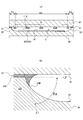
- FIG. 1 is a schematic view showing a configuration example of a conventional organic EL panel having a hollow sealing structure (FIG. 1A is a cross-sectional view, and FIG. 1B is a plan view).
- One or a plurality of organic EL elements J3 for forming the light emitting portion J2 are formed on the substrate J1, and the sealing substrate J5 is bonded to the substrate J1 so as to form a sealing space J4 covering the light emitting portion J2. It is bonded through the layer J6.
- a desiccant J7 is provided on the inner surface of the sealing substrate J5, and the desiccant adsorbs moisture in the sealed space J4 to extend the life of the organic EL element.
- the region where the light emitting part J2 is formed in the surface of the substrate J1 is the light emitting region J20.
- the substrate J1 and the sealing substrate J5 are bonded to the adhesive layer J6.
- it is necessary to form a region (frame region) with a predetermined width JW outside the light emitting region J20 because it is necessary to secure a region (adhesion region) for bonding via the substrate.
- the entire J1 cannot be made the light emitting region J20.
- the frame area outside the light emitting area J20 be as small as possible in order to avoid pressure on the surrounding space.
- the frame region becomes large. There are problems that the number of panels that can be taken out from one large substrate is reduced, the manufacturing yield is poor, and the productivity improvement effect cannot be obtained sufficiently.
- the frame area of each panel is an area that does not emit light and is located within the entire light emitting area of the large area panel. In order to improve the performance of the entire light emitting region, it is required to make the frame region as small as possible.
- the width of the bonding area (see JW1 in FIG. 1) must be reduced. If the width of the bonding area is simply reduced, the bonding strength between the substrate J1 and the sealing substrate J5 is increased. There is a problem that the sufficient sealing performance of the organic EL element J3 cannot be maintained due to insufficient securing.
- the width of the rib portion J10 formed on the sealing substrate J5 to form the sealing space J4 is narrowed. According to this, the strength of the rib portion J10 decreases, and the rib portion J10 cannot withstand the load acting on the sealing substrate J6, and the rib portion J10 is damaged.
- the rib portion J10 is broken, the organic EL element J3 is exposed to the outside air, and there is a problem that the deterioration of the organic EL element J3 proceeds remarkably.
- the strength of the rib portion J10 is reduced, the rib portion J10 may be damaged during the manufacturing process of the organic EL panel, resulting in a decrease in yield.
- the present invention is an example of a problem to deal with such a problem. That is, to increase the occupancy ratio of the light emitting area in the organic EL panel, to improve the performance of the organic EL panel, to narrow the frame area of the organic EL panel, sufficiently ensure the adhesive strength between the substrate and the sealing substrate, It is an object of the present invention to maintain good sealing performance of the organic EL element, to ensure the strength of the rib portion of the sealing substrate, and to prevent problems due to damage of the rib portion.
- the organic EL panel and the manufacturing method thereof according to the present invention include at least the following components.
- the angle formed between the steep tangent line that contacts the side surface of the rib part and the line along the bonding surface in the cross section of the adhesive layer forming portion of the portion is 65 ° to 85 °, and An organic EL panel, wherein the adhesive layer is formed over the side surface of the rib portion.
- the angle formed between the steep tangent line in contact with the side surface of the rib portion and the line along the bonding surface is 65 ° to 85 ° in the cross section of the rib portion at the adhesive layer forming portion.
- the method for manufacturing an organic EL panel is characterized in that the sealing substrate is processed and the adhesive layer is formed from the adhesive surface to the side surface of the rib portion in the sealing step.
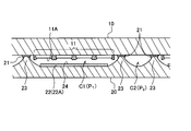
- FIG. 2 is a conceptual diagram showing a basic configuration of an organic EL panel according to an embodiment of the present invention (FIG. 2A shows an overall cross section, and FIG. 2B shows formation of an adhesive layer. Partial enlarged cross section is shown.)
- the organic EL panel 1 includes a substrate 10, a light emitting unit 11 formed on a substrate made of a light-transmitting material, and a sealing substrate 20.
- the light emitting unit 11 includes one or a plurality of organic EL elements 11A in which an anode, an organic layer, and a cathode are stacked.
- the organic EL elements 11A serving as pixels are arranged in a dot matrix to form an image display surface. is doing.
- the organic EL element 11A formed on a substrate formed of a light-transmitting material as in this example can emit light to the outside through the substrate 10 (bottom emission type).
- the organic EL panel 1 according to the embodiment of the present invention may be one that emits light to the outside from the sealing substrate 20 side described later (top emission type). It may be one that emits light from both sides of the sealing substrate 20 to the outside (dual emission type).
- the sealing substrate 20 is bonded to the substrate 10 via an adhesive layer 21 in order to hollow-seal the light emitting unit 11 in the sealing space C.
- the sealing substrate 20 includes a concave portion 22 that accommodates the light emitting portion 11 and a rib portion 23 that is formed along the outer periphery of the concave portion 22 and has an adhesive surface 23 ⁇ / b> A that faces the substrate 10.
- a desiccant 24 is provided on the bottom surface 22A of the recess 22 of the sealing substrate 20 as necessary.
- the organic EL panel 1 according to the embodiment of the present invention having such a panel structure expands the light emitting area EA of the light emitting section 11 to further enlarge the frame area FA (from the outer peripheral edge of the light emitting section 11 to the outer peripheral edge of the substrate 10.
- the adhesive strength between the substrate 10 and the sealing substrate 20 can be secured, and the structural strength of the sealing space of the sealing substrate 20 can be secured.
- the rib part 23 extends from the top part to the root part. Therefore, the structural strength of the rib portion 23 can be ensured. Further, the adhesive applied to the adhesive surface 23A is spread in the sealing space C when the substrate 10 and the sealing substrate 20 are bonded together, but the inclined surface of the angle ⁇ a formed on the side surface of the rib portion 23, The adhesive layer 21 is gradually formed wider from the top of the side surface 23 ⁇ / b> B of the rib portion 23 toward the substrate 10. Thereby, even when the adhesive surface 23A is narrowed, the adhesive force of the adhesive layer 21 can be secured, and the adhesive strength between the substrate 10 and the sealing substrate 20 can be maintained at a sufficient strength.
- the range of the angle ⁇ a is preferably in the range of 65 ° to 85 °.
- the angle ⁇ a is greater than 85 °, so that the rise of the entire rib portion 23 becomes steep, so that the width of the entire rib portion 23 is narrowed by narrowing the bonding surface 23A of the rib portion 23, and the structure of the rib portion 23 is reduced. Strength cannot be obtained.
- the rib portion 23 is damaged, the organic EL element 11 ⁇ / b> A is exposed to the outside air, and the organic EL element 11 ⁇ / b> A deteriorates significantly.
- the organic EL panel 1 is intended to improve the display performance by enlarging the light emitting area EA (narrowing the area of the frame area FA) and improving the effective display area ratio of the panel. Can do. At that time, the sealing performance of the organic EL element 11A can be maintained satisfactorily, and the above-described display performance can be improved while effectively suppressing the deterioration of the light emission characteristics.
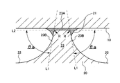
- FIG. 3 is an explanatory view showing an example of formation of the organic EL panel 1 according to the embodiment of the present invention (the same parts as those described above are denoted by the same reference numerals and description thereof is partially omitted).
- an example in which a plurality of sealing spaces are formed by bonding the substrate 10 and the sealing substrate 20 is shown.
- the sealing spaces C1 and C2 are formed on both sides straddling the rib portion 23, in the organic EL panel 1 according to the embodiment of the present invention, from the adhesive surface 23A of the rib portion 23 to both side surfaces 23B.
- An adhesive layer 21 is formed across.
- the volumes of the sealing spaces C1 and C2 adjacent to both sides of the rib portion 23 may be different.
- the substrate 10 and the sealing substrate 20 are bonded to each other in the sealing spaces C1 and C2.
- a difference occurs between the generated internal pressures P1 and P2, and the internal pressure P2 of the sealing space C2 having a small volume becomes higher than the internal pressure P2 of the sealing space C1 having a large volume (P1 ⁇ P2).
- the phenomenon that the adhesive is pulled toward the lower internal pressure due to the internal pressure difference (adhesion of the adhesive) occurs, and this facilitates the movement of the adhesive along the adhesive surface 23A.
- the adhesive layer 21 When such adhesive shrinkage occurs, the adhesive layer 21 is formed to be biased to one side of the rib portion 23, and good adhesive strength cannot be obtained. In addition, the amount of adhesive in the adhesive surface 23A may be reduced or lost due to the shrinkage of the adhesive layer 21, and in this case, the sealing performance is deteriorated or the organic EL element 11A is significantly deteriorated. A problem that progresses occurs.
- the angle ⁇ a By setting the angle ⁇ a to 65 ° or more, the difference between the internal pressures P1 and P2 generated in the sealed spaces C1 and C2 becomes small.
- the adhesive layer 21 spreading in a well-balanced manner on both the left and right sides can be formed, and good adhesive strength and sealing performance between the substrate 10 and the sealing substrate 20 can be ensured.
- FIG. 4 is an explanatory view showing another example of forming the organic EL panel 1 according to the embodiment of the present invention (the same parts as those described above are denoted by the same reference numerals, and a part of the description is omitted).
- the corners of the bonding surface 23 ⁇ / b> A and the side surface 23 ⁇ / b> B are chamfered at the top of the rib portion 23.
- the chamfer R as shown in the figure, the spread of the adhesive layer 21 in the vicinity of the adhesive surface 23A can be more sufficiently secured. Thereby, even when the width of the adhesive surface 23A is narrowed, the adhesive strength of the adhesive layer 21 can be further increased.
- FIG. 5 is an explanatory view showing another example of formation of the organic EL panel 1 according to the embodiment of the present invention (the same parts as those described above are denoted by the same reference numerals and description thereof is partially omitted).
- the recess 22 of the sealing substrate 20 has a stepped shape. That is, a recess 22 ⁇ / b> B is further formed on the bottom surface 22 ⁇ / b> A of the recess 22.
- the concave portion 22 in a multi-step shape like this, the volume of the sealed space can be secured regardless of the prescribed range of the angle ⁇ a, and the space for disposing the desiccant 24 disposed in the sealed space. Can be secured.
- the processing depth is deep and it may be difficult to form the angle ⁇ a at a predetermined value.
- the concave portion 22 is formed in a multi-step moat shape to eliminate the restriction on the formation of the angle ⁇ a.
- the manufacturing method of the organic EL panel 1 according to the embodiment of the present invention includes a light emitting unit forming process as a process on the substrate 10 side, a sealing substrate processing process as a process on the sealing substrate 20 side, and the substrate 10 and the sealing substrate 20. It has a sealing step of bonding.
- the light emitting portion forming step is a step of forming the light emitting portion 11 including at least one organic EL element 11A on the substrate 10.
- the organic EL element 11A has a structure in which an anode, an organic layer, and a cathode are laminated, and an electrode pattern of one of the anode and the cathode is formed on the substrate 10 directly or via another layer, and is insulated and partitioned.
- An organic layer including a light emitting layer is laminated on the electrode pattern, and the other electrode pattern of the anode or the cathode is formed on the organic layer.
- a stripe-shaped transparent electrode is formed on the substrate 10 and an insulating film pattern is formed so as to partition the single organic EL element 11A. Then, a stripe-shaped partition is formed on the insulating film in a direction intersecting with the transparent electrode described above. Then, an organic layer including a light emitting layer is formed on a transparent electrode that is insulated and partitioned, and a metal electrode (cathode) patterned by a partition is formed on the organic layer.
- a pixel electrode (anode) made of a transparent electrode is formed on a substrate 10 on which a driving element such as a TFT is formed via a planarizing film, and insulated.
- An organic layer including a light emitting layer is formed on the partitioned pixel electrode, and a metal electrode (cathode) is further formed on the organic layer.
- the sealing substrate processing step is a step of forming the concave portion 22 that accommodates the light emitting portion 11 in the sealing substrate 20 and the rib portion 23 having the adhesive surface 23A along the outer periphery of the concave portion 22.
- the concave portion 22 and the rib portion 23 can be simultaneously formed by performing a digging process on the surface of the flat sealing substrate 22 while leaving the adhesive surface 23A.
- a processing method such as wet etching, dry etching, or sand blasting can be employed.
- wet etching a resist pattern corresponding to the adhesive surface 23A is formed on the sealing substrate 22, and the exposed surface of the sealing substrate 22 is immersed in an etching solution.
- a resist film having an opening pattern along the outer edge of the concave portion 22 is formed on the surface of the sealing substrate 20, and a first etching process is performed on the pattern. Thereafter, a resist film having an opening pattern is formed inside the recess 22 and a second etching process is performed on the pattern.
- the setting range of the angle ⁇ a described above is realized by appropriately setting the processing conditions at the time of the digging processing for forming the recess 22.
- the sealing step is a step of sealing the light emitting unit 11 in a hollow state by bonding the substrate 10 and the sealing substrate 20 through the adhesive layer 21.
- An appropriate amount of adhesive is applied on the adhesive surface 23A of the sealing substrate 20.
- the amount of adhesive to be applied is set so that the adhesive layer 21 is formed from the adhesive surface 23A to the side surface 23B of the rib portion 23 after bonding.
- the substrate 10 and the sealing substrate 20 are bonded to each other and pressed at a predetermined pressure, whereby the adhesive layer 21 that gradually becomes wider from the top of the side surface of the rib portion 23 toward the substrate 10 is formed.
- an ultraviolet curable resin or a thermosetting resin can be used as the adhesive.
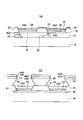
- FIG. 6 is an explanatory view showing an example of forming an organic EL element formed by the light emitting part forming step described above.
- FIG. 4A shows an example of an active drive element having independent pixel electrodes
- FIG. 4B shows an example of a passive drive element in which elements are formed at the intersections of stripe-shaped electrodes. ing.
- a planarizing film 31 is formed on the substrate 10 on which the driving element (TFT or the like) 30 is formed so as to cover the driving element 30, and becomes a pixel electrode on the planarizing film 31.
- a lower electrode 32 is formed.
- the lower electrode 32 can be formed by forming an electrode material on the planarizing film 31 and then patterning it by a photolithography process.
- a connection line 30A for connecting the lower electrode 32 and the drive element 30 is formed, and an insulating film 33 is formed in the peripheral portion thereof.
- An organic layer 34 including a light emitting layer 34A is formed so as to cover the opening pattern of the insulating film 33 on the lower electrode 32.
- the organic layer 34 can be obtained by mask vapor deposition in which the mask opening is combined with the opening of the insulating film 33. Thereafter, the upper electrode 34 is formed so as to cover the entire organic layer 34.
- the lower electrode 40 is formed in a stripe shape on the substrate 10, the insulating film 41 is formed thereon, and a stripe pattern is formed so as to intersect the lower electrode 40.
- stripe-shaped partition walls 42 are formed on the insulating film 41 as necessary. More preferably, the partition wall 42 has a side wall with a reverse taper inclined downward. Then, the organic layer 43 including the light emitting layer 43A is formed along the stripe-shaped opening portions of the insulating film 41 and the partition wall 42, and the stripe-shaped upper electrode 44 is formed thereon.
- the partition wall 42 becomes a mask pattern when the upper electrode 44 is formed.
- the organic material deposition layer 43R and the upper electrode material deposition layer 44R are deposited on the upper surface of the partition wall 42.
- the lower electrodes 32 and 40 can be formed of a transparent electrode such as ITO.
- a hole injection layer such as copper phthalocyanine (CuPc) is formed on the lower electrodes 32 and 40, and, for example, NPB (N, N-di (naphtalence) -N, N-dipheneyl-benzidene) is deposited as a hole transport layer.
- the hole transport layer has a function of transporting holes injected from the lower electrodes 32 and 40 to the light emitting layers 34A and 43A.
- the hole transport layer may be a single layer or a stack of two or more layers.
- the hole transport layer is not formed by a single material, but a single layer may be formed by a plurality of materials, and a guest material having a high charge donating (accepting) property may be formed on a host material having a high charge transport capability. Doping may be performed.
- red (R), green (G), and blue (B) light emitting layers 34A and 43A are formed in respective film forming regions by using a resistance heating vapor deposition method using a coating mask.
- red (R) an organic material that emits red light such as a styryl dye such as DCM1 (4- (dicyanomethylene) -2-methyl-6- (4′-dimethylaminostyryl) -4H-pyran) is used.
- An organic material that emits green light such as an aluminum quinolinol complex (Alq 3 ) is used as green (G).
- an organic material emitting blue light such as a distyryl derivative or a triazole derivative is used.
- a distyryl derivative or a triazole derivative is used.
- other materials or a host-guest layer structure may be used, and the light emission form may be a fluorescent light emitting material or a phosphorescent light emitting material.
- the electron transport layer formed on the light emitting layers 34A and 43A is formed using various materials such as an aluminum quinolinol complex (Alq 3 ) by various film forming methods such as resistance heating vapor deposition.
- the electron transport layer has a function of transporting electrons injected from the upper electrodes 35 and 44 to the light emitting layers 34A and 43A.
- This electron transport layer may have a multilayer structure in which only one layer is stacked or two or more layers are stacked.
- the electron transport layer may be formed of a plurality of materials instead of a single material, and a guest material having a high charge donating (accepting) property may be formed on a host material having a high charge transport capability. It may be formed by doping.
- the insulating films 33 and 41 and the partition wall 42 are made of polyimide or a resist material.
- a material having a work function lower than that of the anode is used so as to have an electron injection function.
- ITO indium gallium
- Al aluminum
- Mg—Ag magnesium alloy
- Al since Al has a low electron injection capability, it is preferable to provide an electron injection layer such as LiF between Al and the electron transport layer.
- the organic EL element 11A Good sealing performance could be obtained. Accordingly, when the organic EL panel according to the embodiment of the present invention is incorporated in a display device in an electronic device or the like, an installation space required for the incorporation can be reduced with respect to a desired display area, and thus the electronic device can be easily downsized. An effect is obtained. Even when it is arranged indoors or in a vehicle as a single display device, desired display performance can be obtained without pressing the surrounding space. Further, when a large number of panels are simultaneously formed on a large substrate, the number of panels can be increased by reducing the area of the frame area FA, the product yield can be improved, and the productivity can be improved.
- a large panel tilting panel
- the area of the non-light emitting area existing in the entire light emitting area of the large panel can be reduced, and the display performance in the large panel can be reduced. Can be improved.
Landscapes
- Electroluminescent Light Sources (AREA)
Abstract
Description
10:基板,11:発光部,11A:有機EL素子,
20:封止基板,21:接着剤層,22:凹部,
23:リブ部,23A:接着面,23B:側面,
24:乾燥剤,
EA:発光領域,FA:額縁領域,C:封止空間,
θa:接線L1と線L2とのなす角度,
Claims (9)
- 基板と、該基板上に形成され、陽極と有機層と陰極が積層された有機EL素子を少なくとも一つ備える発光部と、該発光部を中空封止するために前記基板に接着剤層を介して貼り合わせられる封止基板とを備え、
前記封止基板は、前記発光部を収容する凹部と該凹部の外周に沿って形成され前記基板に対面する接着面を有するリブ部を備え、
前記リブ部の接着剤層形成部分における横断面で、前記リブ部の側面に接する最も急峻な接線と前記接着面に沿った線とのなす角度が65°~85°になり、且つ前記接着面から前記リブ部の側面に渡って前記接着剤層が形成されていることを特徴とする有機ELパネル。 - 前記リブ部の頂部において前記接着面と前記側面との角部を面取したことを特徴とする請求項1記載の有機ELパネル。
- 前記封止基板の凹部を段堀状にしたことを特徴とする請求項1又は2に記載の有機ELパネル。
- 前記接着剤層は、前記リブ部の側面頂部から前記基板に向かって徐々に幅広状に形成されることを特徴とする請求項1~3のいずれかに記載の有機ELパネル。
- 前記封止基板における前記凹部の底面には乾燥剤が配備されることを特徴とする請求項1~4のいずれかに記載の有機ELパネル。
- 基板上に少なくとも一つの有機EL素子を備えた発光部を形成する発光部形成工程と、
封止基板に前記発光部を収容する凹部と該凹部の外周に沿って前記基板に対面する接着面を有するリブ部を形成する封止基板加工工程と、
前記基板と前記封止基板とを接着剤層を介して貼り合わせて前記発光部を中空封止する封止工程とを有し、
前記封止基板加工工程では、前記リブ部の接着剤層形成部分における横断面で、前記リブ部の側面に接する最も急峻な接線と前記接着面に沿った線とのなす角度が65°~85°になるように前記封止基板を加工し、
前記封止工程では、前記接着面から前記リブ部の側面に渡って前記接着剤層を形成することを特徴とする有機ELパネルの製造方法。 - 前記封止基板加工工程では、前記リブ部の頂部において前記接着面と前記側面の角部を面取加工することを特徴とする請求項6記載の有機ELパネルの製造方法。
- 前記封止基板加工工程では、前記凹部をエッチング処理によって形成することを特徴とする請求項6又は7に記載の有機ELパネルの製造方法。
- 前記封止工程では、前記接着面上に接着剤を塗布し、接着剤が塗布された前記封止基板と前記基板とを貼り合わせることを特徴とする請求項6~8のいずれかに記載された有機ELパネルの製造方法。
Priority Applications (3)
| Application Number | Priority Date | Filing Date | Title |
|---|---|---|---|
| JP2011535221A JP5265018B2 (ja) | 2009-10-05 | 2009-10-05 | 有機elパネル及びその製造方法 |
| CN200980161816XA CN102577603A (zh) | 2009-10-05 | 2009-10-05 | 有机el面板及其制造方法 |
| PCT/JP2009/067343 WO2011042944A1 (ja) | 2009-10-05 | 2009-10-05 | 有機elパネル及びその製造方法 |
Applications Claiming Priority (1)
| Application Number | Priority Date | Filing Date | Title |
|---|---|---|---|
| PCT/JP2009/067343 WO2011042944A1 (ja) | 2009-10-05 | 2009-10-05 | 有機elパネル及びその製造方法 |
Publications (1)
| Publication Number | Publication Date |
|---|---|
| WO2011042944A1 true WO2011042944A1 (ja) | 2011-04-14 |
Family
ID=43856445
Family Applications (1)
| Application Number | Title | Priority Date | Filing Date |
|---|---|---|---|
| PCT/JP2009/067343 Ceased WO2011042944A1 (ja) | 2009-10-05 | 2009-10-05 | 有機elパネル及びその製造方法 |
Country Status (3)
| Country | Link |
|---|---|
| JP (1) | JP5265018B2 (ja) |
| CN (1) | CN102577603A (ja) |
| WO (1) | WO2011042944A1 (ja) |
Cited By (2)
| Publication number | Priority date | Publication date | Assignee | Title |
|---|---|---|---|---|
| JP2020021558A (ja) * | 2018-07-30 | 2020-02-06 | 双葉電子工業株式会社 | 有機el素子及びその製造方法 |
| JP2021521473A (ja) * | 2018-04-13 | 2021-08-26 | サムソン ディスプレイ カンパニー リミテッド | 表示装置及びその製造方法 |
Citations (13)
| Publication number | Priority date | Publication date | Assignee | Title |
|---|---|---|---|---|
| JPH11185956A (ja) * | 1997-12-18 | 1999-07-09 | Tdk Corp | 有機el素子の製造方法および有機el素子 |
| JP2000068046A (ja) * | 1998-08-17 | 2000-03-03 | Matsushita Electric Ind Co Ltd | 電場発光デバイス |
| JP2000123968A (ja) * | 1998-10-19 | 2000-04-28 | Toyota Motor Corp | 有機el表示装置およびその製造方法 |
| JP2004079467A (ja) * | 2002-08-22 | 2004-03-11 | Nippon Sheet Glass Co Ltd | El素子用封止板、及び該封止板多面取り用マザーガラス基板 |
| JP2004085769A (ja) * | 2002-08-26 | 2004-03-18 | Hitachi Displays Ltd | 画像表示装置およびその製造方法 |
| JP2005063701A (ja) * | 2003-08-20 | 2005-03-10 | Tohoku Pioneer Corp | フラットパネル表示装置及びその製造方法 |
| JP2006351299A (ja) * | 2005-06-14 | 2006-12-28 | Tohoku Pioneer Corp | 自発光パネル、自発光パネル用の封止部材、および自発光パネルの製造方法 |
| JP2007005060A (ja) * | 2005-06-22 | 2007-01-11 | Fuji Electric Holdings Co Ltd | 有機elディスプレイの製造方法 |
| JP2007095430A (ja) * | 2005-09-28 | 2007-04-12 | Optrex Corp | 有機el表示パネルおよびその製造方法 |
| JP2008066126A (ja) * | 2006-09-07 | 2008-03-21 | Pentax Corp | 封止部材、及び有機エレクトロルミネセンス素子 |
| JP2008077855A (ja) * | 2006-09-19 | 2008-04-03 | Konica Minolta Holdings Inc | 有機エレクトロルミネッセンスパネル、有機エレクトロルミネッセンスパネルの製造方法 |
| JP2008140615A (ja) * | 2006-11-30 | 2008-06-19 | Optrex Corp | 光学パネルの製造方法 |
| JP2009134984A (ja) * | 2007-11-30 | 2009-06-18 | Seiko Epson Corp | 有機エレクトロルミネッセンス装置およびその製造方法 |
Family Cites Families (3)
| Publication number | Priority date | Publication date | Assignee | Title |
|---|---|---|---|---|
| JP3682860B2 (ja) * | 2001-05-16 | 2005-08-17 | 日本精機株式会社 | 有機elパネル及びその製造方法 |
| JP2005351299A (ja) * | 2004-06-08 | 2005-12-22 | Komatsu Gas Kk | 燃料ガス供給設備 |
| JP2006331905A (ja) * | 2005-05-27 | 2006-12-07 | Optrex Corp | 光学パネルの製造方法 |
-
2009
- 2009-10-05 CN CN200980161816XA patent/CN102577603A/zh active Pending
- 2009-10-05 WO PCT/JP2009/067343 patent/WO2011042944A1/ja not_active Ceased
- 2009-10-05 JP JP2011535221A patent/JP5265018B2/ja not_active Expired - Fee Related
Patent Citations (13)
| Publication number | Priority date | Publication date | Assignee | Title |
|---|---|---|---|---|
| JPH11185956A (ja) * | 1997-12-18 | 1999-07-09 | Tdk Corp | 有機el素子の製造方法および有機el素子 |
| JP2000068046A (ja) * | 1998-08-17 | 2000-03-03 | Matsushita Electric Ind Co Ltd | 電場発光デバイス |
| JP2000123968A (ja) * | 1998-10-19 | 2000-04-28 | Toyota Motor Corp | 有機el表示装置およびその製造方法 |
| JP2004079467A (ja) * | 2002-08-22 | 2004-03-11 | Nippon Sheet Glass Co Ltd | El素子用封止板、及び該封止板多面取り用マザーガラス基板 |
| JP2004085769A (ja) * | 2002-08-26 | 2004-03-18 | Hitachi Displays Ltd | 画像表示装置およびその製造方法 |
| JP2005063701A (ja) * | 2003-08-20 | 2005-03-10 | Tohoku Pioneer Corp | フラットパネル表示装置及びその製造方法 |
| JP2006351299A (ja) * | 2005-06-14 | 2006-12-28 | Tohoku Pioneer Corp | 自発光パネル、自発光パネル用の封止部材、および自発光パネルの製造方法 |
| JP2007005060A (ja) * | 2005-06-22 | 2007-01-11 | Fuji Electric Holdings Co Ltd | 有機elディスプレイの製造方法 |
| JP2007095430A (ja) * | 2005-09-28 | 2007-04-12 | Optrex Corp | 有機el表示パネルおよびその製造方法 |
| JP2008066126A (ja) * | 2006-09-07 | 2008-03-21 | Pentax Corp | 封止部材、及び有機エレクトロルミネセンス素子 |
| JP2008077855A (ja) * | 2006-09-19 | 2008-04-03 | Konica Minolta Holdings Inc | 有機エレクトロルミネッセンスパネル、有機エレクトロルミネッセンスパネルの製造方法 |
| JP2008140615A (ja) * | 2006-11-30 | 2008-06-19 | Optrex Corp | 光学パネルの製造方法 |
| JP2009134984A (ja) * | 2007-11-30 | 2009-06-18 | Seiko Epson Corp | 有機エレクトロルミネッセンス装置およびその製造方法 |
Cited By (3)
| Publication number | Priority date | Publication date | Assignee | Title |
|---|---|---|---|---|
| JP2021521473A (ja) * | 2018-04-13 | 2021-08-26 | サムソン ディスプレイ カンパニー リミテッド | 表示装置及びその製造方法 |
| JP7350008B2 (ja) | 2018-04-13 | 2023-09-25 | サムソン ディスプレイ カンパニー リミテッド | 表示装置及びその製造方法 |
| JP2020021558A (ja) * | 2018-07-30 | 2020-02-06 | 双葉電子工業株式会社 | 有機el素子及びその製造方法 |
Also Published As
| Publication number | Publication date |
|---|---|
| JPWO2011042944A1 (ja) | 2013-02-28 |
| CN102577603A (zh) | 2012-07-11 |
| JP5265018B2 (ja) | 2013-08-14 |
Similar Documents
| Publication | Publication Date | Title |
|---|---|---|
| JP5650388B2 (ja) | 有機elパネル、パネル接合型発光装置、有機elパネルの製造方法 | |
| KR100670543B1 (ko) | 유기전계발광 소자 | |
| JP4427054B2 (ja) | 有機電界発光素子及びその製造方法 | |
| CN100471354C (zh) | 有机电致发光显示装置及其制造方法 | |
| US7645176B2 (en) | Organic electro-luminescence display and fabricating method thereof | |
| CN100423318C (zh) | 双面板型有机电致发光显示器件及其制造方法 | |
| US7948160B2 (en) | Optical device and manufacturing method of the optical device | |
| US20060279209A1 (en) | Self-emission panel, self-emission panel sealing member, and self-emission panel manufacturing method | |
| JP5265018B2 (ja) | 有機elパネル及びその製造方法 | |
| KR101752318B1 (ko) | 유기전계 발광소자 제조 방법 | |
| JP2013168381A (ja) | 有機elパネル及びその製造方法 | |
| JP5000128B2 (ja) | 自発光パネル及びその製造方法 | |
| JP2007265859A (ja) | 有機el表示装置 | |
| JP3652136B2 (ja) | 有機elディスプレイパネル及びその製造方法 | |
| KR100749490B1 (ko) | 유기 전계 발광 표시장치 및 이의 제조 방법 | |
| JP5622854B2 (ja) | 有機elパネル及びパネル接合型発光装置 | |
| JP2008300332A (ja) | 有機el表示パネル及びその製造方法 | |
| JP2008108680A (ja) | 有機el素子の製造方法 | |
| JP2008288031A (ja) | El表示装置 | |
| JP2006147192A (ja) | 表示装置 | |
| JP2007335590A (ja) | 有機el素子 | |
| WO2010023746A1 (ja) | 有機elパネル | |
| JP2009059532A (ja) | 有機el表示装置 | |
| JP2005259573A (ja) | 有機elパネルとその製造方法 | |
| WO2010097917A1 (ja) | El表示パネル |
Legal Events
| Date | Code | Title | Description |
|---|---|---|---|
| WWE | Wipo information: entry into national phase |
Ref document number: 200980161816.X Country of ref document: CN |
|
| 121 | Ep: the epo has been informed by wipo that ep was designated in this application |
Ref document number: 09850217 Country of ref document: EP Kind code of ref document: A1 |
|
| WWE | Wipo information: entry into national phase |
Ref document number: 2011535221 Country of ref document: JP |
|
| NENP | Non-entry into the national phase |
Ref country code: DE |
|
| 122 | Ep: pct application non-entry in european phase |
Ref document number: 09850217 Country of ref document: EP Kind code of ref document: A1 |