WO2011040458A1 - 異方性導電フィルム及びその製造方法 - Google Patents
異方性導電フィルム及びその製造方法 Download PDFInfo
- Publication number
- WO2011040458A1 WO2011040458A1 PCT/JP2010/066938 JP2010066938W WO2011040458A1 WO 2011040458 A1 WO2011040458 A1 WO 2011040458A1 JP 2010066938 W JP2010066938 W JP 2010066938W WO 2011040458 A1 WO2011040458 A1 WO 2011040458A1
- Authority
- WO
- WIPO (PCT)
- Prior art keywords
- resin
- anisotropic conductive
- conductive film
- film
- resin layer
- Prior art date
- Legal status (The legal status is an assumption and is not a legal conclusion. Google has not performed a legal analysis and makes no representation as to the accuracy of the status listed.)
- Ceased
Links
- XDTMQSROBMDMFD-UHFFFAOYSA-N C1CCCCC1 Chemical compound C1CCCCC1 XDTMQSROBMDMFD-UHFFFAOYSA-N 0.000 description 1
Images




Classifications
-
- H—ELECTRICITY
- H01—ELECTRIC ELEMENTS
- H01B—CABLES; CONDUCTORS; INSULATORS; SELECTION OF MATERIALS FOR THEIR CONDUCTIVE, INSULATING OR DIELECTRIC PROPERTIES
- H01B5/00—Non-insulated conductors or conductive bodies characterised by their form
- H01B5/16—Non-insulated conductors or conductive bodies characterised by their form comprising conductive material in insulating or poorly conductive material, e.g. conductive rubber
-
- C—CHEMISTRY; METALLURGY
- C09—DYES; PAINTS; POLISHES; NATURAL RESINS; ADHESIVES; COMPOSITIONS NOT OTHERWISE PROVIDED FOR; APPLICATIONS OF MATERIALS NOT OTHERWISE PROVIDED FOR
- C09J—ADHESIVES; NON-MECHANICAL ASPECTS OF ADHESIVE PROCESSES IN GENERAL; ADHESIVE PROCESSES NOT PROVIDED FOR ELSEWHERE; USE OF MATERIALS AS ADHESIVES
- C09J7/00—Adhesives in the form of films or foils
- C09J7/10—Adhesives in the form of films or foils without carriers
-
- C—CHEMISTRY; METALLURGY
- C09—DYES; PAINTS; POLISHES; NATURAL RESINS; ADHESIVES; COMPOSITIONS NOT OTHERWISE PROVIDED FOR; APPLICATIONS OF MATERIALS NOT OTHERWISE PROVIDED FOR
- C09J—ADHESIVES; NON-MECHANICAL ASPECTS OF ADHESIVE PROCESSES IN GENERAL; ADHESIVE PROCESSES NOT PROVIDED FOR ELSEWHERE; USE OF MATERIALS AS ADHESIVES
- C09J9/00—Adhesives characterised by their physical nature or the effects produced, e.g. glue sticks
- C09J9/02—Electrically-conducting adhesives
-
- H—ELECTRICITY
- H01—ELECTRIC ELEMENTS
- H01B—CABLES; CONDUCTORS; INSULATORS; SELECTION OF MATERIALS FOR THEIR CONDUCTIVE, INSULATING OR DIELECTRIC PROPERTIES
- H01B13/00—Apparatus or processes specially adapted for manufacturing conductors or cables
-
- H—ELECTRICITY
- H01—ELECTRIC ELEMENTS
- H01R—ELECTRICALLY-CONDUCTIVE CONNECTIONS; STRUCTURAL ASSOCIATIONS OF A PLURALITY OF MUTUALLY-INSULATED ELECTRICAL CONNECTING ELEMENTS; COUPLING DEVICES; CURRENT COLLECTORS
- H01R11/00—Individual connecting elements providing two or more spaced connecting locations for conductive members which are, or may be, thereby interconnected, e.g. end pieces for wires or cables supported by the wire or cable and having means for facilitating electrical connection to some other wire, terminal, or conductive member, blocks of binding posts
- H01R11/01—Individual connecting elements providing two or more spaced connecting locations for conductive members which are, or may be, thereby interconnected, e.g. end pieces for wires or cables supported by the wire or cable and having means for facilitating electrical connection to some other wire, terminal, or conductive member, blocks of binding posts characterised by the form or arrangement of the conductive interconnection between the connecting locations
-
- H—ELECTRICITY
- H01—ELECTRIC ELEMENTS
- H01R—ELECTRICALLY-CONDUCTIVE CONNECTIONS; STRUCTURAL ASSOCIATIONS OF A PLURALITY OF MUTUALLY-INSULATED ELECTRICAL CONNECTING ELEMENTS; COUPLING DEVICES; CURRENT COLLECTORS
- H01R12/00—Structural associations of a plurality of mutually-insulated electrical connecting elements, specially adapted for printed circuits, e.g. printed circuit boards [PCB], flat or ribbon cables, or like generally planar structures, e.g. terminal strips, terminal blocks; Coupling devices specially adapted for printed circuits, flat or ribbon cables, or like generally planar structures; Terminals specially adapted for contact with, or insertion into, printed circuits, flat or ribbon cables, or like generally planar structures
- H01R12/50—Fixed connections
- H01R12/59—Fixed connections for flexible printed circuits, flat or ribbon cables or like structures
- H01R12/62—Fixed connections for flexible printed circuits, flat or ribbon cables or like structures connecting to rigid printed circuits or like structures
-
- H—ELECTRICITY
- H01—ELECTRIC ELEMENTS
- H01R—ELECTRICALLY-CONDUCTIVE CONNECTIONS; STRUCTURAL ASSOCIATIONS OF A PLURALITY OF MUTUALLY-INSULATED ELECTRICAL CONNECTING ELEMENTS; COUPLING DEVICES; CURRENT COLLECTORS
- H01R12/00—Structural associations of a plurality of mutually-insulated electrical connecting elements, specially adapted for printed circuits, e.g. printed circuit boards [PCB], flat or ribbon cables, or like generally planar structures, e.g. terminal strips, terminal blocks; Coupling devices specially adapted for printed circuits, flat or ribbon cables, or like generally planar structures; Terminals specially adapted for contact with, or insertion into, printed circuits, flat or ribbon cables, or like generally planar structures
- H01R12/70—Coupling devices
- H01R12/7076—Coupling devices for connection between PCB and component, e.g. display
-
- H—ELECTRICITY
- H01—ELECTRIC ELEMENTS
- H01R—ELECTRICALLY-CONDUCTIVE CONNECTIONS; STRUCTURAL ASSOCIATIONS OF A PLURALITY OF MUTUALLY-INSULATED ELECTRICAL CONNECTING ELEMENTS; COUPLING DEVICES; CURRENT COLLECTORS
- H01R4/00—Electrically-conductive connections between two or more conductive members in direct contact, i.e. touching one another; Means for effecting or maintaining such contact; Electrically-conductive connections having two or more spaced connecting locations for conductors and using contact members penetrating insulation
- H01R4/04—Electrically-conductive connections between two or more conductive members in direct contact, i.e. touching one another; Means for effecting or maintaining such contact; Electrically-conductive connections having two or more spaced connecting locations for conductors and using contact members penetrating insulation using electrically conductive adhesives
-
- H—ELECTRICITY
- H05—ELECTRIC TECHNIQUES NOT OTHERWISE PROVIDED FOR
- H05K—PRINTED CIRCUITS; CASINGS OR CONSTRUCTIONAL DETAILS OF ELECTRIC APPARATUS; MANUFACTURE OF ASSEMBLAGES OF ELECTRICAL COMPONENTS
- H05K3/00—Apparatus or processes for manufacturing printed circuits
- H05K3/30—Assembling printed circuits with electric components, e.g. with resistors
- H05K3/32—Assembling printed circuits with electric components, e.g. with resistors electrically connecting electric components or wires to printed circuits
- H05K3/321—Assembling printed circuits with electric components, e.g. with resistors electrically connecting electric components or wires to printed circuits by conductive adhesives
- H05K3/323—Assembling printed circuits with electric components, e.g. with resistors electrically connecting electric components or wires to printed circuits by conductive adhesives by applying an anisotropic conductive adhesive layer over an array of pads
-
- H—ELECTRICITY
- H10—SEMICONDUCTOR DEVICES; ELECTRIC SOLID-STATE DEVICES NOT OTHERWISE PROVIDED FOR
- H10W—GENERIC PACKAGES, INTERCONNECTIONS, CONNECTORS OR OTHER CONSTRUCTIONAL DETAILS OF DEVICES COVERED BY CLASS H10
- H10W72/00—Interconnections or connectors in packages
- H10W72/071—Connecting or disconnecting
- H10W72/073—Connecting or disconnecting of die-attach connectors
-
- C—CHEMISTRY; METALLURGY
- C08—ORGANIC MACROMOLECULAR COMPOUNDS; THEIR PREPARATION OR CHEMICAL WORKING-UP; COMPOSITIONS BASED THEREON
- C08K—Use of inorganic or non-macromolecular organic substances as compounding ingredients
- C08K9/00—Use of pretreated ingredients
- C08K9/02—Ingredients treated with inorganic substances
-
- C—CHEMISTRY; METALLURGY
- C09—DYES; PAINTS; POLISHES; NATURAL RESINS; ADHESIVES; COMPOSITIONS NOT OTHERWISE PROVIDED FOR; APPLICATIONS OF MATERIALS NOT OTHERWISE PROVIDED FOR
- C09J—ADHESIVES; NON-MECHANICAL ASPECTS OF ADHESIVE PROCESSES IN GENERAL; ADHESIVE PROCESSES NOT PROVIDED FOR ELSEWHERE; USE OF MATERIALS AS ADHESIVES
- C09J2203/00—Applications of adhesives in processes or use of adhesives in the form of films or foils
- C09J2203/326—Applications of adhesives in processes or use of adhesives in the form of films or foils for bonding electronic components such as wafers, chips or semiconductors
-
- C—CHEMISTRY; METALLURGY
- C09—DYES; PAINTS; POLISHES; NATURAL RESINS; ADHESIVES; COMPOSITIONS NOT OTHERWISE PROVIDED FOR; APPLICATIONS OF MATERIALS NOT OTHERWISE PROVIDED FOR
- C09J—ADHESIVES; NON-MECHANICAL ASPECTS OF ADHESIVE PROCESSES IN GENERAL; ADHESIVE PROCESSES NOT PROVIDED FOR ELSEWHERE; USE OF MATERIALS AS ADHESIVES
- C09J2301/00—Additional features of adhesives in the form of films or foils
- C09J2301/20—Additional features of adhesives in the form of films or foils characterized by the structural features of the adhesive itself
- C09J2301/208—Additional features of adhesives in the form of films or foils characterized by the structural features of the adhesive itself the adhesive layer being constituted by at least two or more adjacent or superposed adhesive layers, e.g. multilayer adhesive
-
- C—CHEMISTRY; METALLURGY
- C09—DYES; PAINTS; POLISHES; NATURAL RESINS; ADHESIVES; COMPOSITIONS NOT OTHERWISE PROVIDED FOR; APPLICATIONS OF MATERIALS NOT OTHERWISE PROVIDED FOR
- C09J—ADHESIVES; NON-MECHANICAL ASPECTS OF ADHESIVE PROCESSES IN GENERAL; ADHESIVE PROCESSES NOT PROVIDED FOR ELSEWHERE; USE OF MATERIALS AS ADHESIVES
- C09J2301/00—Additional features of adhesives in the form of films or foils
- C09J2301/40—Additional features of adhesives in the form of films or foils characterized by the presence of essential components
- C09J2301/408—Additional features of adhesives in the form of films or foils characterized by the presence of essential components additives as essential feature of the adhesive layer
-
- H—ELECTRICITY
- H05—ELECTRIC TECHNIQUES NOT OTHERWISE PROVIDED FOR
- H05K—PRINTED CIRCUITS; CASINGS OR CONSTRUCTIONAL DETAILS OF ELECTRIC APPARATUS; MANUFACTURE OF ASSEMBLAGES OF ELECTRICAL COMPONENTS
- H05K2203/00—Indexing scheme relating to apparatus or processes for manufacturing printed circuits covered by H05K3/00
- H05K2203/11—Treatments characterised by their effect, e.g. heating, cooling, roughening
- H05K2203/1189—Pressing leads, bumps or a die through an insulating layer
-
- H—ELECTRICITY
- H05—ELECTRIC TECHNIQUES NOT OTHERWISE PROVIDED FOR
- H05K—PRINTED CIRCUITS; CASINGS OR CONSTRUCTIONAL DETAILS OF ELECTRIC APPARATUS; MANUFACTURE OF ASSEMBLAGES OF ELECTRICAL COMPONENTS
- H05K3/00—Apparatus or processes for manufacturing printed circuits
- H05K3/36—Assembling printed circuits with other printed circuits
- H05K3/361—Assembling flexible printed circuits with other printed circuits
-
- H—ELECTRICITY
- H10—SEMICONDUCTOR DEVICES; ELECTRIC SOLID-STATE DEVICES NOT OTHERWISE PROVIDED FOR
- H10W—GENERIC PACKAGES, INTERCONNECTIONS, CONNECTORS OR OTHER CONSTRUCTIONAL DETAILS OF DEVICES COVERED BY CLASS H10
- H10W72/00—Interconnections or connectors in packages
- H10W72/071—Connecting or disconnecting
- H10W72/073—Connecting or disconnecting of die-attach connectors
- H10W72/07331—Connecting techniques
-
- H—ELECTRICITY
- H10—SEMICONDUCTOR DEVICES; ELECTRIC SOLID-STATE DEVICES NOT OTHERWISE PROVIDED FOR
- H10W—GENERIC PACKAGES, INTERCONNECTIONS, CONNECTORS OR OTHER CONSTRUCTIONAL DETAILS OF DEVICES COVERED BY CLASS H10
- H10W72/00—Interconnections or connectors in packages
- H10W72/30—Die-attach connectors
- H10W72/321—Structures or relative sizes of die-attach connectors
- H10W72/322—Multilayered die-attach connectors, e.g. a coating on a top surface of a core
-
- H—ELECTRICITY
- H10—SEMICONDUCTOR DEVICES; ELECTRIC SOLID-STATE DEVICES NOT OTHERWISE PROVIDED FOR
- H10W—GENERIC PACKAGES, INTERCONNECTIONS, CONNECTORS OR OTHER CONSTRUCTIONAL DETAILS OF DEVICES COVERED BY CLASS H10
- H10W72/00—Interconnections or connectors in packages
- H10W72/30—Die-attach connectors
- H10W72/321—Structures or relative sizes of die-attach connectors
- H10W72/325—Die-attach connectors having a filler embedded in a matrix
-
- H—ELECTRICITY
- H10—SEMICONDUCTOR DEVICES; ELECTRIC SOLID-STATE DEVICES NOT OTHERWISE PROVIDED FOR
- H10W—GENERIC PACKAGES, INTERCONNECTIONS, CONNECTORS OR OTHER CONSTRUCTIONAL DETAILS OF DEVICES COVERED BY CLASS H10
- H10W72/00—Interconnections or connectors in packages
- H10W72/30—Die-attach connectors
- H10W72/351—Materials of die-attach connectors
-
- H—ELECTRICITY
- H10—SEMICONDUCTOR DEVICES; ELECTRIC SOLID-STATE DEVICES NOT OTHERWISE PROVIDED FOR
- H10W—GENERIC PACKAGES, INTERCONNECTIONS, CONNECTORS OR OTHER CONSTRUCTIONAL DETAILS OF DEVICES COVERED BY CLASS H10
- H10W72/00—Interconnections or connectors in packages
- H10W72/30—Die-attach connectors
- H10W72/351—Materials of die-attach connectors
- H10W72/352—Materials of die-attach connectors comprising metals or metalloids, e.g. solders
-
- H—ELECTRICITY
- H10—SEMICONDUCTOR DEVICES; ELECTRIC SOLID-STATE DEVICES NOT OTHERWISE PROVIDED FOR
- H10W—GENERIC PACKAGES, INTERCONNECTIONS, CONNECTORS OR OTHER CONSTRUCTIONAL DETAILS OF DEVICES COVERED BY CLASS H10
- H10W72/00—Interconnections or connectors in packages
- H10W72/30—Die-attach connectors
- H10W72/351—Materials of die-attach connectors
- H10W72/353—Materials of die-attach connectors not comprising solid metals or solid metalloids, e.g. ceramics
- H10W72/354—Materials of die-attach connectors not comprising solid metals or solid metalloids, e.g. ceramics comprising polymers
Definitions
- the present invention relates to an anisotropic conductive film in which conductive particles are dispersed and a method for producing the same.
- an SMD (Surface Mount Device) 101 such as a capacitor is mounted on the FPC 102, and the IC 103 is mounted on the glass substrate 104.
- the FPC 102 and the glass substrate 104 are connected by an ACF (Anisotropic Conductive Film) 105 for FOG (Film ⁇ on Glass), and the IC 103 and the glass substrate 104 are connected by an ACF 106 for COG.
- the soldering method is used for the mounting method of the SMD 101 and the reflow process is essential, the SMD 101 is heated at a high temperature.
- a double-sided FPC 102 is required for joining the SMD 101, which increases the cost.
- the number of SMDs 101 required has increased with the recent increase in detail of liquid crystal devices, and the liquid crystal devices have become larger due to the increase in the FPC 102 area.
- the present invention has been proposed in view of such a conventional situation, and provides an anisotropic conductive film in which electronic parts having different sizes are simultaneously mounted with high accuracy and a method for manufacturing the same.
- tack force which is one of the ability to hold a surface-mounted component, and by using an ACF having a two-layer structure, on the glass substrate. It was found that SMD can be temporarily mounted at high speed, and SMD and IC can be mounted simultaneously.
- the anisotropic conductive film according to the present invention is characterized in that a first resin layer having a tack force of 200 kPa or more and a second resin layer containing conductive particles are laminated.
- a first resin layer having a tack force of 200 kPa or more and a second resin layer containing conductive particles are laminated, and a surface mounter is used.
- a plurality of electronic components are temporarily mounted on the first resin layer, and an anisotropic conductive film used for simultaneously mounting the electronic component and another electronic component by thermocompression bonding is manufactured.
- a small SMD can be temporarily mounted at a high speed by a high tack force, and the particle capturing property in COG, for example, can be improved by a two-layer structure. Different electronic components can be simultaneously mounted with high accuracy.
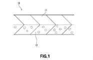
- FIG. 1 is a cross-sectional view showing an anisotropic conductive film according to an embodiment of the present invention.
- FIG. 2 is a diagram schematically illustrating an example of a product form of the anisotropic conductive film.
- FIG. 3 is a view for explaining a mounting method of an electronic component using the anisotropic conductive film according to the present embodiment.
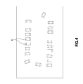
- FIG. 4 is a schematic diagram of a photograph when a small SMD is temporarily mounted using the anisotropic conductive film of Sample 4.
- FIG. 5 is a schematic diagram of a photograph when a small SMD is temporarily mounted using the anisotropic conductive film of Sample 7.
- FIG. 6 is a diagram for explaining a conventional electronic component mounting method.
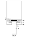
- FIG. 7 is a diagram for explaining a conventional electronic component mounting method.
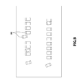
- FIG. 8 is a schematic view of a photograph when a small SMD is temporarily mounted using a conventional anisotropic conductive film.
- FIG. 1 is a cross-sectional view showing an anisotropic conductive film according to an embodiment of the present invention.
- the anisotropic conductive film 10 includes a first resin layer 11 having a tack force of 200 kPa or more and a second resin layer 12 containing conductive particles.
- the anisotropic conductive film 10 has a plurality of electronic components temporarily mounted on the first resin layer 11 by a surface mounter, and the electronic components and other electronic components are simultaneously mounted by thermocompression bonding. Used to do.
- the surface mounter for example, a device that can be temporarily mounted at a high speed of about 1.0 to 0.1 seconds / chip can be used.
- the electronic component temporarily mounted using the surface mounter is not particularly limited as long as it is an SMD (Surface Mount Device) applicable to the surface mounter.
- SMD Surface Mount Device
- a capacitor can be mentioned.
- the tack force of the first resin layer 11 of the anisotropic conductive film according to the present embodiment is 200 kPa or more, thereby preventing misalignment when temporarily mounting a small SMD such as a capacitor at a high speed. It can be mounted with high accuracy.
- the range of tack force is preferably 200 to 600 kPa, and more preferably 200 to 250 kPa. Within this range, sufficient holding force for high-speed temporary mounting of electronic components can be obtained, and the film shape can be maintained.
- the tack force means the maximum value of the adhesive force in the process of pressing the measuring probe controlled by the tacking tester (TACKINESS TESTER) against the object to be measured and pulling it away.
- the first resin layer 11 is an insulating layer not containing conductive particles
- the second resin layer 12 is a conductive layer containing conductive particles
- the anisotropic conductive film according to the present embodiment is It is preferable to have a two-layer structure in which the first resin layer 11 and the second resin layer are laminated.
- the first resin layer 11 flows due to the pressing force of the bumps of the IC, and the electrode on the glass substrate is electrically conductive. It will be in the state which does not prevent contact with particle
- the second resin layer 12 contains conductive particles at a high density, the flow due to the pressing force of the bumps of the IC is limited, and the conductive particles are captured at a high capture rate.
- the capture rate of conductive particles means the ratio of the number of conductive particles per unit area of terminals (bumps) before and after joining the electronic component and the substrate.
- the minimum melt viscosity of the second resin layer 12 is preferably higher than the minimum melt viscosity of the first resin layer 11.
- the minimum melt viscosity of the resin constituting the second resin layer 12 is preferably 100 to 100,000 Pa ⁇ s, and the minimum melt viscosity of the resin constituting the first resin layer 11 is 10 to 100 It is preferably 10,000 Pa ⁇ s.
- the minimum melt viscosity can be measured by loading a sample in a predetermined amount on a rotary viscometer and increasing the sample at a predetermined temperature increase rate.
- the conductive particles used in the anisotropic conductive film 10 are not particularly limited, and examples thereof include metal particles such as nickel, gold, and copper, resin particles that are plated with gold, and resin particles that are plated with gold.
- the outermost layer of the particles may be an insulating coating.
- the anisotropic conductive film 10 preferably has a viscosity at room temperature of 10 to 1000 kPa ⁇ s, more preferably 10 to 500 kPa.
- a viscosity at room temperature 10 to 1000 kPa ⁇ s, more preferably 10 to 500 kPa.
- the composition of the first resin layer 11 and the second resin layer 12 is not particularly limited as long as the above-described characteristics are not impaired, but more preferably, a film-forming resin, a liquid epoxy resin, and a latent curing agent. And a silane coupling agent.
- the film-forming resin corresponds to a high molecular weight resin having an average molecular weight of 10,000 or more, and preferably has an average molecular weight of about 10,000 to 80,000 from the viewpoint of film formation.
- various resins such as epoxy resin, modified epoxy resin, modified epoxy resin, urethane resin, phenoxy resin and the like can be used. Among them, phenoxy resin is used from the viewpoint of film formation state, connection reliability, etc. Preferably used.
- the liquid epoxy resin is not particularly limited as long as it has fluidity at room temperature, and all commercially available epoxy resins can be used.
- Specific examples of such epoxy resins include naphthalene type epoxy resins, biphenyl type epoxy resins, phenol novolac type epoxy resins, bisphenol type epoxy resins, stilbene type epoxy resins, triphenolmethane type epoxy resins, phenol aralkyl type epoxy resins.
- Resins, naphthol type epoxy resins, dicyclopentadiene type epoxy resins, triphenylmethane type epoxy resins, and the like can be used. These may be used alone or in combination of two or more.
- the latent curing agent various curing agents such as a heat curing type and a UV curing type can be used.
- the latent curing agent does not normally react but is activated by some trigger and starts the reaction.
- the trigger includes heat, light, pressurization, etc., and can be selected and used depending on the application.
- the activation method of the thermally activated latent curing agent includes a method of generating active species (cations and anions) by a dissociation reaction by heating, and the like.
- Thermally active latent curing agents include imidazole, hydrazide, boron trifluoride-amine complexes, sulfonium salts, amine imides, polyamine salts, dicyandiamide, etc., and modified products thereof. These may be used alone or in combination of two or more. Can be used as a mixture. Among these, in this Embodiment, a microcapsule type imidazole-type latent hardening
- curing agent is used preferably.
- silane coupling agent epoxy, amino, mercapto sulfide, ureido, etc. can be used.
- an epoxy-type silane coupling agent is used preferably. Thereby, the adhesiveness in the interface of an organic material and an inorganic material can be improved.
- an inorganic filler as another additive composition.
- silica, talc, titanium oxide, calcium carbonate, magnesium oxide and the like can be used, and the kind of the inorganic filler is not particularly limited.
- FIG. 2 is a diagram schematically illustrating an example of a product form of the anisotropic conductive film 10.
- anisotropic conductive film 10 a first resin layer 11 and a second resin layer 12 are laminated on a release substrate 13 in this order, and are molded into a tape shape.
- This tape-like anisotropic conductive film is wound and laminated on the winding portion 22 sandwiched between the first and second flanges 21 so that the peeling substrate 13 is on the outer peripheral side.
- the peeling base material 13 PET (Poly Ethylene Terephthalate), OPP (Oriented Polypropylene), PMP (Poly-4-methlpentene-1), PTFE (Polytetrafluoroethylene) etc. can be used. Moreover, it is good also as a structure which has a transparent cover film on the 2nd resin layer 12.
- the anisotropic conductive film 10 is not limited to a reel shape, and may be a strip shape.
- the anisotropic conductive film 10 when the anisotropic conductive film 10 is provided as a reel product, the anisotropic conductive film 10 has a viscosity in the range of 10 to 1000 kPa ⁇ s. Deformation of the film 10 can be prevented and a predetermined dimension can be maintained. Similarly, when two or more anisotropic conductive films 10 are stacked in a strip shape, deformation can be prevented and a predetermined dimension can be maintained.
- the tack force of the first resin layer 11 is made larger than the tack force of the second resin layer 12, whereby the second resin layer 12. Is peeled from the peeling substrate 13 first, and blocking can be prevented.
- a first resin film having a tack force of 200 kPa or more is formed on a second resin film containing conductive particles.
- the first resin film and the second resin film may be attached, or after forming one resin film, the other resin may be applied and dried (overcoated).
- the 1st resin film and the 2nd resin film comprise the 1st resin layer 11 and the 2nd resin layer 12, respectively.
- the manufacturing method of attaching the first resin film and the second resin film includes a step of generating a first resin film having a tack force of 200 kPa or more, and a second resin film containing conductive particles. And a step of attaching the first resin film and the second resin film.
- the film-forming resin, the liquid epoxy resin, the latent curing agent, and the silane coupling agent are dissolved in a solvent.
- the solvent toluene, ethyl acetate or the like, or a mixed solvent thereof can be used.
- the 1st resin film is obtained by apply
- the conductive particles, the film-forming resin, the liquid epoxy resin, the latent curing agent, and the silane coupling agent are dissolved in a solvent.
- a solvent toluene, ethyl acetate or the like, or a mixed solvent thereof can be used.
- the 2nd resin film is obtained by apply
- the release sheet of the second resin film is peeled off and attached onto the first resin film.
- the first resin layer 11 and the second resin layer 12 are laminated in this order on the peeling substrate 13.
- the conductive film 10 can be obtained.
- the second resin film generating solution is added to the first resin film. What is necessary is just to apply
- FIG. 3 is a view for explaining a method of mounting an electronic component using the anisotropic conductive film according to the present embodiment.
- the SMD 31, the FPC 32, and the IC 33 are each connected to the electrode of the glass substrate by the anisotropic conductive film 10.
- the SMD 31 is a capacitor, and is temporarily mounted on the first resin layer side of the anisotropic conductive film 10 using a surface mounter at the time of mounting, and the FPC 32 and the IC 33 are other than the first resin layer. Placed in the mounting area. Then, for example, these electronic components are collectively thermocompression bonded using a thermocompression bonding head, whereby the SMD 31, the FPC 32, and the IC 33 are electrically connected to the electrodes of the glass substrate.
- the anisotropic conductive film 10 is disposed over the entire surface of the mounting region including the electrodes on the glass substrate, and different mounting-type electronic components (SMD31, FPC32, and IC33) are disposed at the electrode positions on the anisotropic conductive film 10.
- SMD31, FPC32, and IC33 different mounting-type electronic components
- the tact time can be greatly improved as compared with the case of using the conventional solder joint, by arranging the electronic components and collectively thermocompressing these electronic components using, for example, a thermocompression bonding head.
- the SMD bonding is changed from the conventionally used solder to the ACF, thereby enabling high-speed mounting.
- phenoxy resin, liquid epoxy resin, latent curing agent, silane coupling agent, silica particles, and conductive particles are dissolved in toluene so that the mixing ratio shown in Table 1 is obtained.
- the liquid was coated on the release film so as to have a predetermined dry thickness, and dried in an oven to prepare resins A to G.
- PKHH is a phenoxy resin manufactured by Phenoxy Associates.
- EP828 is a bisphenol A liquid epoxy resin manufactured by Japan Epoxy Range Co., Ltd.
- HX3941 is a microcapsule type imidazole-based latent curing agent manufactured by Asahi Kasei Chemical Co., Ltd.
- A-187 is an epoxy silane coupling agent manufactured by Momentive Performance Materials Japan GK.
- RY200 is a hydrophobic silica particle manufactured by Nippon Aerosil Co., Ltd.
- the “Ni / Au plated acrylic resin particles” are conductive particles manufactured by Sekisui Chemical Co., Ltd.
- each compounding ratio in Table 1 shows a mass part.
- anisotropic conductive film samples 1 to 7 were prepared using the resins A to G shown in Table 1.
- Example 1 An anisotropic conductive film having a one-layer structure made of resin F having a thickness of 25 ⁇ m was produced.
- Example 2 An anisotropic conductive film having a single-layer structure made of resin G having a thickness of 25 ⁇ m was produced.
- Example 3 A first resin film made of a resin A having a film thickness of 15 ⁇ m and a second resin film made of a resin G having a film thickness of 10 ⁇ m were attached to produce an anisotropic conductive film having a two-layer structure.
- anisotropic conductive film having a two-layer structure.
- Example 4 A first resin film made of a resin B having a film thickness of 15 ⁇ m and a second resin film made of a resin G having a film thickness of 10 ⁇ m were attached to produce a two-layer anisotropic conductive film.
- the electronic component is mounted on the glass substrate using this anisotropic conductive film, it is fixed so that the electronic component side is the first resin film and the glass substrate side is the second resin film, as in Sample 3.
- Example 5 A first resin film made of a resin C having a film thickness of 15 ⁇ m and a second resin film made of a resin G having a film thickness of 10 ⁇ m were pasted to produce a two-layer anisotropic conductive film.
- the electronic component is mounted on the glass substrate using this anisotropic conductive film, it is fixed so that the electronic component side is the first resin film and the glass substrate side is the second resin film, as in Sample 3.
- Example 6 A first resin film made of a resin D having a film thickness of 15 ⁇ m and a second resin film made of a resin G having a film thickness of 10 ⁇ m were pasted to produce a two-layer anisotropic conductive film.
- the electronic component is mounted on the glass substrate using this anisotropic conductive film, it is fixed so that the electronic component side is the first resin film and the glass substrate side is the second resin film, as in Sample 3.
- Example 7 A first resin film made of a resin E having a film thickness of 15 ⁇ m and a second resin film made of a resin G having a film thickness of 10 ⁇ m were pasted to produce a two-layer anisotropic conductive film.
- the electronic component is mounted on the glass substrate using this anisotropic conductive film, it is fixed so that the electronic component side is the first resin film and the glass substrate side is the second resin film, as in Sample 3.
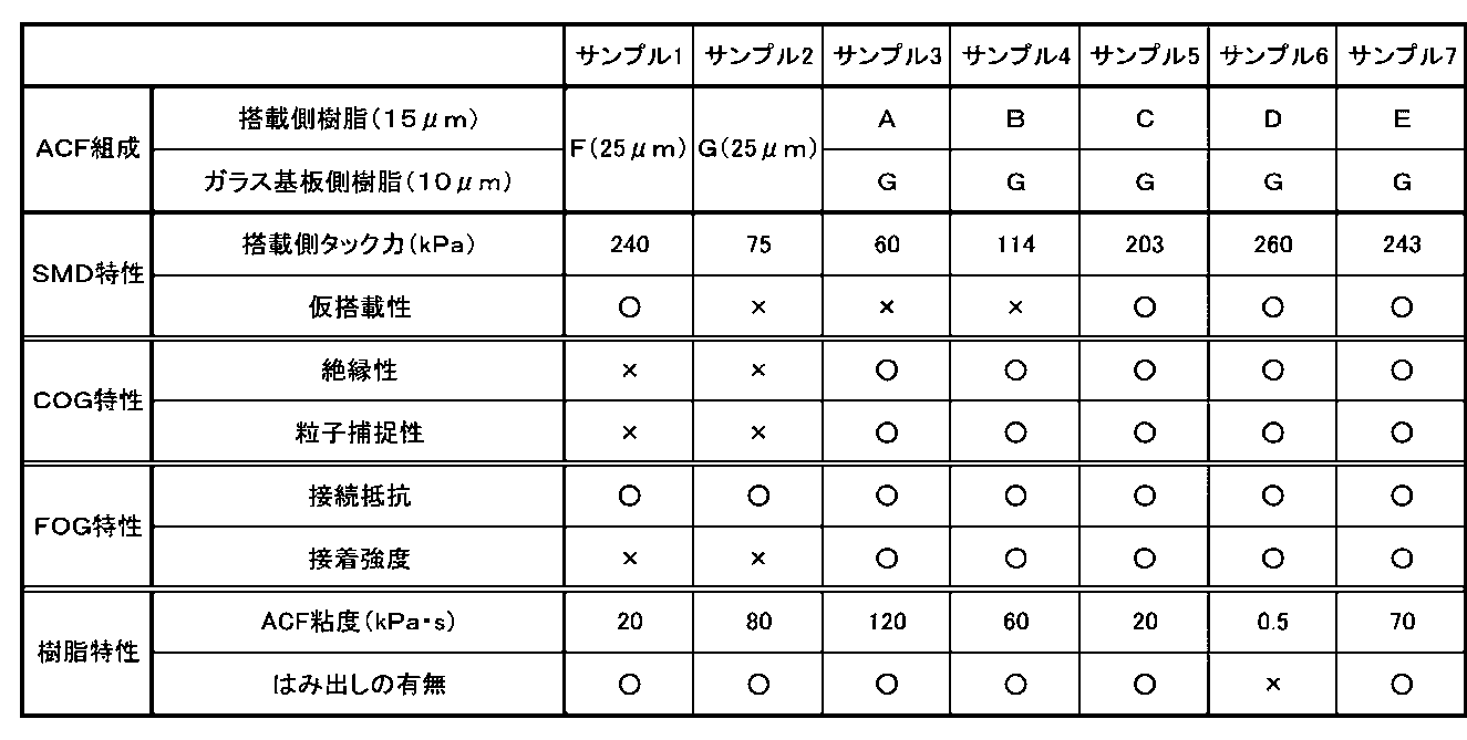
- Table 2 shows the test results of Samples 1-7.
- Each test of tack force, temporary mounting property, insulating property, particle trapping property, connection resistance, adhesive strength, viscosity, and winding property was performed as follows. Samples 1 to 4 correspond to comparative examples or reference examples, and samples 5 to 7 correspond to examples.
- tacking power Using a tack tester (TACII manufactured by Resuka Co., Ltd.), measurement at a probe diameter of 5 mm (stainless steel mirror surface, cylindrical shape), pressing load of 196 kgf, pressing speed of 30 mm / min, peeling speed of 5 mm / min in an atmosphere at 22 ° C. It carried out on condition, and made the peak intensity
- the tack force of each sample represents the tack force of the film on the electronic component mounting side.
- [Insulation] IC space between bumps: 12.5 ⁇ m was thermocompression bonded to each sample on a 0.7 mm thick glass substrate (Corning Corp., 1737F) to obtain a connection body.
- a voltage of 30 V was applied between adjacent pads of the glass substrate to measure the insulation resistance, and the insulation resistance of 1.0 ⁇ 10 ⁇ 6 ⁇ or less was shorted.
- the case of short was set as x, and the case of not short was set as O.
- connection resistance [Connection resistance] IC (space between bumps: 12.5 ⁇ m) was thermocompression bonded to each sample on a 0.7 mm thick glass substrate (Corning Corp., 1737F) to obtain a connection body. Then, the initial connection resistance ( ⁇ ) between the IC bump and the glass substrate pad was measured. The case where the connection resistance was less than 5 ⁇ was O, and the case where the connection resistance was 5 ⁇ or more was rated as x.
- connection strength (space between bumps: 12.5 ⁇ m) was thermocompression bonded to each sample on a 0.7 mm thick glass substrate (Corning Corp., 1737F) to obtain a connection body. And the peeling strength when peeling this connection body in 90 degreeC direction with the tensile strength of 50 cm / min was made into initial stage adhesive strength (N / cm). The case where the adhesive strength was less than 3 N / cm was evaluated as x, and the case where the adhesive strength was 3 N / cm or higher was defined as O.
- the minimum viscosity (kPa ⁇ s) of each sample was measured using a stress-controlled rheometer (Haake RS150). A cone having a diameter of 8 mm and an angle of 2 degrees was used, and the measurement range was 30 ° C. to 250 ° C. Moreover, it measured similarly about the resin film by the side of an electronic component mounting, and the resin film by the side of a glass substrate.
- FIG. 4 is a diagram showing a state in which a small SMD is temporarily mounted using the anisotropic conductive film of Sample 4.
- FIG. 5 is a diagram showing a state in which a small SMD is temporarily mounted using the anisotropic conductive film of Sample 7.
- FIG. 10 SMDs (1005 capacitors manufactured by Murata Manufacturing Co., Ltd.) are arranged on the sample in two rows with a gap of 0.3 mm between elements. Temporary loading.
- the use of sample 7 can maintain the position of the capacitor at high-speed temporary mounting with higher accuracy than the use of sample 4. This is because the resin film E on the mounting side of the sample 7 contains more liquid epoxy resin than the resin film B on the mounting side of the sample 4 and has a high tack force.
- the first resin layer on the electronic component mounting side has a tacking force of 200 kPa or more
- the second resin layer on the glass substrate side contains conductive particles.
- sample 5 to sample 7 have a two-layer structure and have a tacking force of 200 kPa or more, so that capacitors can be temporarily mounted at a high speed and can be mounted simultaneously with electronic components such as IC and FPC. Is possible.
- sample 1 has a tack force of 200 kPa or more, since it is a single layer only of resin film F, good insulation and particle trapping properties cannot be obtained.
- Sample 2 does not have a tack force sufficient for high-speed temporary mounting, and since it is a single layer made of only the resin film G, good insulating properties, particle trapping properties, and adhesive strength can be obtained. It is not suitable for mounting any of IC, FPC and SMD.
- Samples 3 and 4 have a two-layer structure, but the tack force is the same level as that of the conventional ACF, and is not only suitable for high-speed temporary mounting, and is not suitable for SMD mounting. .
- the anisotropic conductive film has a viscosity of 10 to 1000 kPa ⁇ s, it is possible to maintain the film shape and to prevent protrusion when the film is wound on a reel.
- sample 6 and sample 7 have the same blending ratio of the liquid epoxy resin to the phenoxy resin, but sample 6 has a viscosity that is too low, so that protrusion occurs when it is wound on a reel.
- the sample 7 since the sample 7 has an appropriate viscosity, it is possible to prevent the sample 7 from protruding when wound on the reel.
- the blending ratio of the liquid epoxy resin in the first resin layer on the electronic component mounting side is 100 to 150 parts by mass with respect to 100 parts by mass of the phenoxy resin.
- an excellent tack force can be maintained.
- the resin films C to F used on the mounting side of the samples 1 and 5 to 7 are within the above blending ratio range, a tack force of 200 kPa or more can be obtained.
- the resin film E containing silica particles has a liquid epoxy resin content while maintaining the tack force. It is possible to prevent a decrease in viscosity due to an increase in.
Landscapes
- Chemical & Material Sciences (AREA)
- Organic Chemistry (AREA)
- Engineering & Computer Science (AREA)
- Manufacturing & Machinery (AREA)
- Microelectronics & Electronic Packaging (AREA)
- Wire Bonding (AREA)
- Non-Insulated Conductors (AREA)
- Electric Connection Of Electric Components To Printed Circuits (AREA)
- Manufacturing Of Electrical Connectors (AREA)
- Laminated Bodies (AREA)
Abstract
Description
本出願は、日本国において2009年9月30日に出願された日本特許出願番号特願2009-225771を基礎として優先権を主張するものであり、この出願を参照することにより、本出願に援用される。
図1は、本発明の一実施の形態に係る異方性導電フィルムを示す断面図である。この異方性導電フィルム10は、200kPa以上のタック力を有する第1の樹脂層11と、導電性粒子を含有する第2の樹脂層12とが積層されている。この異方性導電フィルム10を用いて電子部品をガラス基板に実装させる場合、電子部品側が第1の樹脂層11、ガラス基板側が第2の樹脂層12となるように固着される。特に、本実施の形態に係る異方性導電フィルム10は、表面実装機によって第1の樹脂層11上に電子部品が複数仮搭載され、熱圧着により電子部品と他の電子部品とを同時実装するのに用いられる。表面実装機としては、例えば1.0~0.1秒/チップ程度に高速仮搭載可能なものを用いることができる。また、表面実装機を用いて仮搭載する電子部品としては、表面実装機に適用可能なSMD(Surface Mount Device)であれば、特に制限されないが、例えば液晶表示装置を製造する際のSMDとしてはコンデンサを挙げることができる。
の観点から、第2の樹脂層12の最低溶融粘度は、第1の樹脂層11の最低溶融粘度よりも高いことが好ましい。具体的には、第2の樹脂層12を構成する樹脂の最低溶融粘度は、100~100000Pa・sであることが好ましく、第1の樹脂層11を構成する樹脂の最低溶融粘度は、10~10000Pa・sであることが好ましい。最低溶融粘度については、サンプルを所定量回転式粘度計に装填し、所定の昇温速度で上昇させながら測定することができる。
12上に透明なカバーフィルムを有する構成としてもよい。また、異方性導電フィルム10は、リール形状に限らず、短冊形状であってもよい。
次に、上述した異方性導電フィルムの製造方法について説明する。本実施の形態における異方性導電フィルムの製造方法は、200kPa以上のタック力を有する第1の樹脂膜を、導電性粒子を含有する第2の樹脂膜上に形成する。ここで、第1の樹脂膜と第2の樹脂膜とを貼り付けてもよいし、一方の樹脂膜を形成後、他方の樹脂を塗布乾燥(重ね塗り)させてもよい。なお、第1の樹脂膜及び第2の樹脂膜は、それぞれ第1の樹脂層11及び第2の樹脂層12を構成する。
次に、異方性導電フィルムを用いた電子部品の実装方法について説明する。本実施の形態に係る異方性導電フィルムは、タック力が高いため小型SMDを高速仮搭載しても位置ずれが生じにくい。また、2層構造であるため、粒子捕捉性が良く、ファインピッチのICを実装することができる。すなわち、本実施の形態に係る異方性導電フィルムによれば、大きさ、種類などの異なる電子部品を一括実装することができる。

膜厚25μmの樹脂Fからなる1層構造の異方性導電フィルムを作製した。
膜厚25μmの樹脂Gからなる1層構造の異方性導電フィルムを作製した。
膜厚15μmの樹脂Aからなる第1の樹脂膜と、膜厚10μmの樹脂Gからなる第2の樹脂膜とを貼り付け、2層構造の異方性導電フィルムを作製した。なお、この異方性導電フィルムを用いて電子部品をガラス基板に実装させる場合は、電子部品側が第1の樹脂膜、ガラス基板側が第2の樹脂膜となるように固着される。
膜厚15μmの樹脂Bからなる第1の樹脂膜と、膜厚10μmの樹脂Gからなる第2の樹脂膜とを貼り付け、2層構造の異方性導電フィルムを作製した。なお、この異方性導電フィルムを用いて電子部品をガラス基板に実装させる場合は、サンプル3と同様に電子部品側が第1の樹脂膜、ガラス基板側が第2の樹脂膜となるように固着される。
膜厚15μmの樹脂Cからなる第1の樹脂膜と、膜厚10μmの樹脂Gからなる第2の樹脂膜とを貼り付け、2層構造の異方性導電フィルムを作製した。なお、この異方性導電フィルムを用いて電子部品をガラス基板に実装させる場合は、サンプル3と同様に電子部品側が第1の樹脂膜、ガラス基板側が第2の樹脂膜となるように固着される。
膜厚15μmの樹脂Dからなる第1の樹脂膜と、膜厚10μmの樹脂Gからなる第2の樹脂膜とを貼り付け、2層構造の異方性導電フィルムを作製した。なお、この異方性導電フィルムを用いて電子部品をガラス基板に実装させる場合は、サンプル3と同様に電子部品側が第1の樹脂膜、ガラス基板側が第2の樹脂膜となるように固着される。
膜厚15μmの樹脂Eからなる第1の樹脂膜と、膜厚10μmの樹脂Gからなる第2の樹脂膜とを貼り付け、2層構造の異方性導電フィルムを作製した。なお、この異方性導電フィルムを用いて電子部品をガラス基板に実装させる場合は、サンプル3と同様に電子部品側が第1の樹脂膜、ガラス基板側が第2の樹脂膜となるように固着される。
タック試験機((株)レスカ製TACII)を用い、22℃の雰囲気下において、プローブ直径5mm(ステンレス製鏡面、円柱状)、押し付け荷重196kgf、押し付け速度30mm/min、剥離速度5mm/minの測定条件で行い、ピーク強度を各サンプルのタック力(kPa)とした。ここで、各サンプルのタック力は、電子部品搭載側のフィルムのタック力を表す。
表面実装機(ヤマハ発動機(株)社製YV100II)を用いて、0.7mm厚のガラス基板(コーニング(株)製1737F)上の各サンプルに10個のSMD((株)村田製作所製1005コンデンサ、外形寸法:L1.0mm×W0.5mm×H0.4mm)を0.3mmの素子間ギャップで仮搭載した。SMDの位置ずれがある場合を×、位置ずれがない場合をOとした。
0.7mm厚のガラス基板(コーニング(株)製1737F)上の各サンプルにIC(バンプ間スペース:12.5μm)を熱圧着し、接続体を得た。ガラス基板の隣接するパッド間に30Vの電圧を加え絶縁抵抗を測定し、絶縁抵抗が1.0×10⁻⁶Ω以下をショートとした。ショートの場合を×とし、ショートでない場合をOとした。
ICを仮固定した際の各バンプ下に存在する導電性粒子の数(平均)と、熱圧着後の粒子捕捉数(平均)とをカウントし、下記式により捕捉効率を求めた。捕捉効率が20%以上の場合をOとし、20%未満の場合を×とした。
捕捉効率(%)=(熱圧着後に捕捉した粒子数)/(仮固定時バンプ下に存在する粒子数)×100
0.7mm厚のガラス基板(コーニング(株)製1737F)上の各サンプルにIC(バンプ間スペース:12.5μm)を熱圧着し、接続体を得た。そして、ICのバンプとガラス基板のパッド間の初期接続抵抗(Ω)を測定した。接続抵抗が5Ωより小さい場合をO、5Ω以上の場合を×とした。
0.7mm厚のガラス基板(コーニング(株)製1737F)上の各サンプルにIC(バンプ間スペース:12.5μm)を熱圧着し、接続体を得た。そして、この接続体を引張強度50cm/minで90℃方向に剥離したときの剥離強度を初期接着強度(N/cm)とした。接着強度が3N/cmより小さい場合を×とし、3N/cm以上の場合をOとした。
応力制御型レオメータ(Haake社製RS150)を用い、各サンプルの最低粘度(kPa・s)を測定した。コーンとしては直径8mm、角度2度のものを使用し、測定範囲は30℃~250℃とした。また、電子部品搭載側の樹脂フィルム及びガラス基板側の樹脂フィルムについても同様にして測定した。
各サンプルを2.0mmにスリットし、コア直径を2.54mm、外形110mmのリールに0.2N/mm2のテンションで巻き取り、室温で1日放置した。外観観察により、はみ出しが無い場合をOとし、はみ出しが有る場合を×とした。
Claims (7)
- 200kPa以上のタック力を有する第1の樹脂層と、
導電性粒子を含有する第2の樹脂層と
が積層された異方性導電フィルム。 - 常温での粘度が、10~1000kPa・sである請求項1記載の異方性導電フィルム。
- 上記第1の樹脂層及び上記第2の樹脂層が、膜形成樹脂と、液状エポキシ樹脂と、潜在性硬化剤とを含有する請求項2記載の異方性導電フィルム。
- 上記第2の樹脂層が、無機フィラーを含有する請求項3記載の異方性導電フィルム。
- 上記第1の樹脂層が、無機フィラーを含有する請求項4記載の異方性導電フィルム。
- 表面実装機によって上記第1の樹脂層上に電子部品が複数仮搭載され、熱圧着により上記電子部品と他の電子部品とを同時実装するのに用いられる請求項1乃至請求項5のいずれか1項記載の異方性導電フィルム。
- 上記請求項6記載の異方性導電フィルムを製造する製造方法。
Priority Applications (2)
| Application Number | Priority Date | Filing Date | Title |
|---|---|---|---|
| HK13100221.6A HK1174153B (en) | 2009-09-30 | 2010-09-29 | Anisotropic conducting film and method for producing same |
| CN201080054185.4A CN102668250B (zh) | 2009-09-30 | 2010-09-29 | 各向异性导电膜及其制造方法 |
Applications Claiming Priority (2)
| Application Number | Priority Date | Filing Date | Title |
|---|---|---|---|
| JP2009-225771 | 2009-09-30 | ||
| JP2009225771A JP5398455B2 (ja) | 2009-09-30 | 2009-09-30 | 異方性導電フィルム及びその製造方法 |
Publications (1)
| Publication Number | Publication Date |
|---|---|
| WO2011040458A1 true WO2011040458A1 (ja) | 2011-04-07 |
Family
ID=43826274
Family Applications (1)
| Application Number | Title | Priority Date | Filing Date |
|---|---|---|---|
| PCT/JP2010/066938 Ceased WO2011040458A1 (ja) | 2009-09-30 | 2010-09-29 | 異方性導電フィルム及びその製造方法 |
Country Status (5)
| Country | Link |
|---|---|
| JP (1) | JP5398455B2 (ja) |
| KR (1) | KR20120098646A (ja) |
| CN (1) | CN102668250B (ja) |
| TW (1) | TWI456595B (ja) |
| WO (1) | WO2011040458A1 (ja) |
Cited By (1)
| Publication number | Priority date | Publication date | Assignee | Title |
|---|---|---|---|---|
| WO2014034741A1 (ja) * | 2012-08-29 | 2014-03-06 | デクセリアルズ株式会社 | 異方性導電フィルム及びその製造方法 |
Families Citing this family (8)
| Publication number | Priority date | Publication date | Assignee | Title |
|---|---|---|---|---|
| JP5956362B2 (ja) * | 2013-02-19 | 2016-07-27 | デクセリアルズ株式会社 | 異方性導電フィルム、接続方法、及び接合体 |
| KR101665160B1 (ko) * | 2013-05-31 | 2016-10-11 | 제일모직주식회사 | 이방성 도전 필름, 이의 조성물 및 이를 이용한 디스플레이 장치 |
| JP6428325B2 (ja) * | 2014-02-04 | 2018-11-28 | デクセリアルズ株式会社 | 異方性導電フィルム及びその製造方法 |
| JP2015149126A (ja) * | 2014-02-04 | 2015-08-20 | デクセリアルズ株式会社 | 異方性導電フィルム及びその製造方法 |
| TWI711052B (zh) * | 2014-02-04 | 2020-11-21 | 日商迪睿合股份有限公司 | 異向性導電膜及其製造方法 |
| JP6661888B2 (ja) * | 2014-03-31 | 2020-03-11 | デクセリアルズ株式会社 | 異方性導電フィルムの製造方法 |
| TWI755470B (zh) * | 2018-01-16 | 2022-02-21 | 優顯科技股份有限公司 | 導電薄膜、光電半導體裝置及其製造方法 |
| DE102019126859A1 (de) * | 2019-10-07 | 2021-04-08 | OSRAM Opto Semiconductors Gesellschaft mit beschränkter Haftung | Anzeigevorrichtung und Anzeigeeinheit |
Citations (4)
| Publication number | Priority date | Publication date | Assignee | Title |
|---|---|---|---|---|
| JP2006236759A (ja) * | 2005-02-24 | 2006-09-07 | Sony Chemical & Information Device Corp | 絶縁被覆導電粒子 |
| JP2007131649A (ja) * | 2003-09-12 | 2007-05-31 | Sony Chemical & Information Device Corp | 多層異方性導電性接着剤及びこれを用いた接続構造体 |
| JP2007169469A (ja) * | 2005-12-22 | 2007-07-05 | Toray Ind Inc | 電子機器用接着剤組成物、その製造方法、およびそれを用いた電子機器用接着剤シート |
| JP2009013416A (ja) * | 2003-01-07 | 2009-01-22 | Sekisui Chem Co Ltd | 硬化性樹脂組成物、接着性エポキシ樹脂ペースト、接着性エポキシ樹脂シート、導電接続ペースト、導電接続シート及び電子部品接合体 |
Family Cites Families (1)
| Publication number | Priority date | Publication date | Assignee | Title |
|---|---|---|---|---|
| JP5013067B2 (ja) * | 2007-01-22 | 2012-08-29 | ソニーケミカル&インフォメーションデバイス株式会社 | 異方性導電フィルム |
-
2009
- 2009-09-30 JP JP2009225771A patent/JP5398455B2/ja not_active Expired - Fee Related
-
2010
- 2010-09-29 WO PCT/JP2010/066938 patent/WO2011040458A1/ja not_active Ceased
- 2010-09-29 KR KR1020127010312A patent/KR20120098646A/ko not_active Ceased
- 2010-09-29 TW TW099133204A patent/TWI456595B/zh not_active IP Right Cessation
- 2010-09-29 CN CN201080054185.4A patent/CN102668250B/zh not_active Expired - Fee Related
Patent Citations (4)
| Publication number | Priority date | Publication date | Assignee | Title |
|---|---|---|---|---|
| JP2009013416A (ja) * | 2003-01-07 | 2009-01-22 | Sekisui Chem Co Ltd | 硬化性樹脂組成物、接着性エポキシ樹脂ペースト、接着性エポキシ樹脂シート、導電接続ペースト、導電接続シート及び電子部品接合体 |
| JP2007131649A (ja) * | 2003-09-12 | 2007-05-31 | Sony Chemical & Information Device Corp | 多層異方性導電性接着剤及びこれを用いた接続構造体 |
| JP2006236759A (ja) * | 2005-02-24 | 2006-09-07 | Sony Chemical & Information Device Corp | 絶縁被覆導電粒子 |
| JP2007169469A (ja) * | 2005-12-22 | 2007-07-05 | Toray Ind Inc | 電子機器用接着剤組成物、その製造方法、およびそれを用いた電子機器用接着剤シート |
Cited By (2)
| Publication number | Priority date | Publication date | Assignee | Title |
|---|---|---|---|---|
| WO2014034741A1 (ja) * | 2012-08-29 | 2014-03-06 | デクセリアルズ株式会社 | 異方性導電フィルム及びその製造方法 |
| US10412837B2 (en) | 2012-08-29 | 2019-09-10 | Dexerials Corporation | Anisotropic conductive film and method of producing the same |
Also Published As
| Publication number | Publication date |
|---|---|
| JP5398455B2 (ja) | 2014-01-29 |
| CN102668250B (zh) | 2015-06-17 |
| KR20120098646A (ko) | 2012-09-05 |
| TWI456595B (zh) | 2014-10-11 |
| TW201129994A (en) | 2011-09-01 |
| JP2011076808A (ja) | 2011-04-14 |
| CN102668250A (zh) | 2012-09-12 |
| HK1174153A1 (en) | 2013-05-31 |
Similar Documents
| Publication | Publication Date | Title |
|---|---|---|
| JP5398455B2 (ja) | 異方性導電フィルム及びその製造方法 | |
| JP5388572B2 (ja) | 導電粒子配置シート及び異方導電性フィルム | |
| CN101755022B (zh) | 粘合薄膜、连接方法及接合体 | |
| JP5192194B2 (ja) | 接着フィルム | |
| JP6245792B2 (ja) | 導電性粒子、回路接続材料、実装体、及び実装体の製造方法 | |
| JP2009013416A (ja) | 硬化性樹脂組成物、接着性エポキシ樹脂ペースト、接着性エポキシ樹脂シート、導電接続ペースト、導電接続シート及び電子部品接合体 | |
| JP3441412B2 (ja) | 樹脂封止型半導体装置およびこれを用いた液晶表示モジュール | |
| CN102844936B (zh) | 电子部件的连接方法及连接结构体 | |
| EP1657725B1 (en) | Insulation-coated electroconductive particles | |
| JP2000080341A (ja) | 異方性導電接着剤および基板搭載デバイス | |
| CN113728402B (zh) | 连接结构体、连接结构体的制造方法、连接材料和被覆导电颗粒 | |
| JP5543267B2 (ja) | 異方性導電フィルム及びその製造方法、並びに実装体及びその製造方法 | |
| JP2005197032A (ja) | 異方導電性フィルム | |
| JP3981341B2 (ja) | 異方導電性接着剤 | |
| JPH02288019A (ja) | 異方性導電フィルム | |
| JP4993877B2 (ja) | 異方導電性接着シート及び微細接続構造体 | |
| JPH09115335A (ja) | 異方性導電接着フィルム | |
| JP4684087B2 (ja) | 連結構造体 | |
| Matsuda et al. | Interconnection technologies of anisotropic conductive films and their application to flexible electronics | |
| WO2016163226A1 (ja) | 異方性導電フィルム、及び接続方法 | |
| HK1174153B (en) | Anisotropic conducting film and method for producing same | |
| HK1177331A (en) | Method for connecting electronic part and connecting structure |
Legal Events
| Date | Code | Title | Description |
|---|---|---|---|
| WWE | Wipo information: entry into national phase |
Ref document number: 201080054185.4 Country of ref document: CN |
|
| 121 | Ep: the epo has been informed by wipo that ep was designated in this application |
Ref document number: 10820573 Country of ref document: EP Kind code of ref document: A1 |
|
| DPE1 | Request for preliminary examination filed after expiration of 19th month from priority date (pct application filed from 20040101) | ||
| NENP | Non-entry into the national phase |
Ref country code: DE |
|
| ENP | Entry into the national phase |
Ref document number: 20127010312 Country of ref document: KR Kind code of ref document: A |
|
| 122 | Ep: pct application non-entry in european phase |
Ref document number: 10820573 Country of ref document: EP Kind code of ref document: A1 |