WO2011039907A1 - 半導体装置及びその製造方法 - Google Patents
半導体装置及びその製造方法 Download PDFInfo
- Publication number
- WO2011039907A1 WO2011039907A1 PCT/JP2010/003814 JP2010003814W WO2011039907A1 WO 2011039907 A1 WO2011039907 A1 WO 2011039907A1 JP 2010003814 W JP2010003814 W JP 2010003814W WO 2011039907 A1 WO2011039907 A1 WO 2011039907A1
- Authority
- WO
- WIPO (PCT)
- Prior art keywords
- insulating film
- light shielding
- gate electrode
- back gate
- semiconductor device
- Prior art date
- Legal status (The legal status is an assumption and is not a legal conclusion. Google has not performed a legal analysis and makes no representation as to the accuracy of the status listed.)
- Ceased
Links
Images













Classifications
-
- G—PHYSICS
- G02—OPTICS
- G02F—OPTICAL DEVICES OR ARRANGEMENTS FOR THE CONTROL OF LIGHT BY MODIFICATION OF THE OPTICAL PROPERTIES OF THE MEDIA OF THE ELEMENTS INVOLVED THEREIN; NON-LINEAR OPTICS; FREQUENCY-CHANGING OF LIGHT; OPTICAL LOGIC ELEMENTS; OPTICAL ANALOGUE/DIGITAL CONVERTERS
- G02F1/00—Devices or arrangements for the control of the intensity, colour, phase, polarisation or direction of light arriving from an independent light source, e.g. switching, gating or modulating; Non-linear optics
- G02F1/01—Devices or arrangements for the control of the intensity, colour, phase, polarisation or direction of light arriving from an independent light source, e.g. switching, gating or modulating; Non-linear optics for the control of the intensity, phase, polarisation or colour
- G02F1/13—Devices or arrangements for the control of the intensity, colour, phase, polarisation or direction of light arriving from an independent light source, e.g. switching, gating or modulating; Non-linear optics for the control of the intensity, phase, polarisation or colour based on liquid crystals, e.g. single liquid crystal display cells
- G02F1/133—Constructional arrangements; Operation of liquid crystal cells; Circuit arrangements
- G02F1/136—Liquid crystal cells structurally associated with a semi-conducting layer or substrate, e.g. cells forming part of an integrated circuit
- G02F1/1362—Active matrix addressed cells
- G02F1/136213—Storage capacitors associated with the pixel electrode
-
- G—PHYSICS
- G02—OPTICS
- G02F—OPTICAL DEVICES OR ARRANGEMENTS FOR THE CONTROL OF LIGHT BY MODIFICATION OF THE OPTICAL PROPERTIES OF THE MEDIA OF THE ELEMENTS INVOLVED THEREIN; NON-LINEAR OPTICS; FREQUENCY-CHANGING OF LIGHT; OPTICAL LOGIC ELEMENTS; OPTICAL ANALOGUE/DIGITAL CONVERTERS
- G02F1/00—Devices or arrangements for the control of the intensity, colour, phase, polarisation or direction of light arriving from an independent light source, e.g. switching, gating or modulating; Non-linear optics
- G02F1/01—Devices or arrangements for the control of the intensity, colour, phase, polarisation or direction of light arriving from an independent light source, e.g. switching, gating or modulating; Non-linear optics for the control of the intensity, phase, polarisation or colour
- G02F1/13—Devices or arrangements for the control of the intensity, colour, phase, polarisation or direction of light arriving from an independent light source, e.g. switching, gating or modulating; Non-linear optics for the control of the intensity, phase, polarisation or colour based on liquid crystals, e.g. single liquid crystal display cells
- G02F1/133—Constructional arrangements; Operation of liquid crystal cells; Circuit arrangements
- G02F1/136—Liquid crystal cells structurally associated with a semi-conducting layer or substrate, e.g. cells forming part of an integrated circuit
- G02F1/1362—Active matrix addressed cells
- G02F1/136209—Light shielding layers, e.g. black matrix, incorporated in the active matrix substrate, e.g. structurally associated with the switching element
-
- H—ELECTRICITY
- H10—SEMICONDUCTOR DEVICES; ELECTRIC SOLID-STATE DEVICES NOT OTHERWISE PROVIDED FOR
- H10D—INORGANIC ELECTRIC SEMICONDUCTOR DEVICES
- H10D86/00—Integrated devices formed in or on insulating or conducting substrates, e.g. formed in silicon-on-insulator [SOI] substrates or on stainless steel or glass substrates
- H10D86/40—Integrated devices formed in or on insulating or conducting substrates, e.g. formed in silicon-on-insulator [SOI] substrates or on stainless steel or glass substrates characterised by multiple TFTs
- H10D86/411—Integrated devices formed in or on insulating or conducting substrates, e.g. formed in silicon-on-insulator [SOI] substrates or on stainless steel or glass substrates characterised by multiple TFTs characterised by materials, geometry or structure of the substrates
-
- H—ELECTRICITY
- H10—SEMICONDUCTOR DEVICES; ELECTRIC SOLID-STATE DEVICES NOT OTHERWISE PROVIDED FOR
- H10D—INORGANIC ELECTRIC SEMICONDUCTOR DEVICES
- H10D86/00—Integrated devices formed in or on insulating or conducting substrates, e.g. formed in silicon-on-insulator [SOI] substrates or on stainless steel or glass substrates
- H10D86/40—Integrated devices formed in or on insulating or conducting substrates, e.g. formed in silicon-on-insulator [SOI] substrates or on stainless steel or glass substrates characterised by multiple TFTs
- H10D86/60—Integrated devices formed in or on insulating or conducting substrates, e.g. formed in silicon-on-insulator [SOI] substrates or on stainless steel or glass substrates characterised by multiple TFTs wherein the TFTs are in active matrices
-
- G—PHYSICS
- G02—OPTICS
- G02F—OPTICAL DEVICES OR ARRANGEMENTS FOR THE CONTROL OF LIGHT BY MODIFICATION OF THE OPTICAL PROPERTIES OF THE MEDIA OF THE ELEMENTS INVOLVED THEREIN; NON-LINEAR OPTICS; FREQUENCY-CHANGING OF LIGHT; OPTICAL LOGIC ELEMENTS; OPTICAL ANALOGUE/DIGITAL CONVERTERS
- G02F1/00—Devices or arrangements for the control of the intensity, colour, phase, polarisation or direction of light arriving from an independent light source, e.g. switching, gating or modulating; Non-linear optics
- G02F1/01—Devices or arrangements for the control of the intensity, colour, phase, polarisation or direction of light arriving from an independent light source, e.g. switching, gating or modulating; Non-linear optics for the control of the intensity, phase, polarisation or colour
- G02F1/13—Devices or arrangements for the control of the intensity, colour, phase, polarisation or direction of light arriving from an independent light source, e.g. switching, gating or modulating; Non-linear optics for the control of the intensity, phase, polarisation or colour based on liquid crystals, e.g. single liquid crystal display cells
- G02F1/133—Constructional arrangements; Operation of liquid crystal cells; Circuit arrangements
- G02F1/1333—Constructional arrangements; Manufacturing methods
- G02F1/133357—Planarisation layers
-
- H—ELECTRICITY
- H10—SEMICONDUCTOR DEVICES; ELECTRIC SOLID-STATE DEVICES NOT OTHERWISE PROVIDED FOR
- H10D—INORGANIC ELECTRIC SEMICONDUCTOR DEVICES
- H10D30/00—Field-effect transistors [FET]
- H10D30/60—Insulated-gate field-effect transistors [IGFET]
- H10D30/67—Thin-film transistors [TFT]
- H10D30/6704—Thin-film transistors [TFT] having supplementary regions or layers in the thin films or in the insulated bulk substrates for controlling properties of the device
- H10D30/6723—Thin-film transistors [TFT] having supplementary regions or layers in the thin films or in the insulated bulk substrates for controlling properties of the device having light shields
Definitions
- the present invention relates to a semiconductor device used in, for example, a liquid crystal display device and a manufacturing method thereof.
- a liquid crystal display device includes a TFT substrate in which a plurality of TFTs (Thin-FilmTransistors) and pixel electrodes connected to the TFT are arranged in a matrix, a TFT substrate, a color filter, a common electrode, etc. And a liquid crystal layer provided between the counter substrate and the TFT substrate.
- TFTs Thin-FilmTransistors
- a backlight unit as a light source is provided on the opposite side of the liquid crystal layer of the TFT substrate.
- a glass substrate is generally used as the TFT substrate.
- a light-shielding film that shields light from a backlight unit that attempts to enter the TFT, or a so-called back gate electrode, is formed on the TFT substrate.
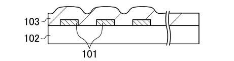
- FIG. 22 which is a sectional view of a conventional semiconductor device
- a light shielding film 101 made of a so-called refractory metal is formed on a glass substrate 102.
- the light shielding film 101 is covered with an insulating film 103.
- a silicon layer 104 is formed in an island shape on the surface of the insulating film 103 so as to overlap the light shielding film 101.
- a gate insulating film 105 is formed on the insulating film 103 so as to cover the silicon layer 104, and a gate electrode 106 is formed on the surface thereof.
- the step shape of the light shielding film 101 is reflected in the silicon layer 104. It is difficult to crystallize with high precision by a laser.
- the flatness of the surface of the silicon layer 104 is impaired by the steps of the light shielding film 101 and the projections of the crystal grain boundaries, it is difficult to make the gate insulating film 105 thin. Therefore, the threshold voltage of the TFT cannot be controlled with high accuracy, and as a result of increasing the power supply voltage, it becomes difficult to reduce the power consumption of the semiconductor device.
- an increase in leakage current due to crystal defects in the semiconductor layer 104 causes an increase in power consumption.
- FIG. 23 to FIG. 25 are cross-sectional views showing manufacturing steps
- a plurality of light shielding films 101 and an insulating film covering the transparent supporting substrate 102 are covered. 103.
- the surface of the insulating film 103 is planarized by a CMP (Chemical-Mechanical-Polishing) method.
- the buried oxide film 107 formed on the surface of the single crystal silicon 108 is bonded to the surface of the planarized insulating film 103.
- the single crystal silicon on the support substrate 102 is thinned to manufacture the TFT.
- FIGS. 26 and 27 are cross-sectional views showing the manufacturing process
- the surface of the silicon substrate 108 is formed in an uneven shape, and the surface is covered with an insulating film 109. .
- an opening 110 is formed in the insulating film 109 in the convex region of the silicon substrate 108.
- the conductive material 112 is polished.
- the back gate electrode 113 is formed by the conductive material layer 112 remaining in the opening 110.
- an interlayer insulating film 114 is formed so as to cover the back gate electrode 113 and the back gate insulating film 111, and the surface of the interlayer insulating film 114 is bonded to a support substrate (not shown).
- the support substrate which is the glass substrate 102 constitutes a display panel of a liquid crystal display device
- the support substrate is a large-sized substrate. Therefore, as in Patent Document 1, it is extremely difficult to polish the insulating film 103 formed on the large support substrate with high accuracy by the CMP method. In recent years, since the glass substrate has been increased in size in order to form many display panels from one surface of the glass substrate, this problem is remarkable.
- the present invention has been made in view of the above points, and the main object of the present invention is to provide a light-shielding film or a back gate electrode for a semiconductor device regardless of the shape of the light-shielding film or the like.
- An object of the present invention is to flatten an insulating layer covering a film or the like with high accuracy.
- the present invention is directed to a method for manufacturing a semiconductor device.
- a step of forming a plurality of light shielding films or back gate electrodes, and a second insulating film that covers the light shielding films or back gate electrodes and has an uneven surface reflecting the step shape of the light shielding films or back gate electrodes The step of forming on the surface of the first insulating film and the surface of the second insulating film between the adjacent light shielding films or between the adjacent back gate electrodes from the surface of the first insulating film Forming a dummy pattern having a height equal to the surface height of the second insulating film on the light-shielding film or the back gate electrode; covering the dummy pattern on the surface of the second insulating film; surface A step of forming a third insulating film, a step of attaching the base layer provided with the third insulating film to a support substrate on a flat surface of the third insulating film, and a step of attaching the base layer to the support substrate.
- a step of separating and removing a part of the base layer along the release layer and a base layer remaining on the support substrate are used to form a semiconductor layer constituting a semiconductor element, and at least a part of the semiconductor layer is the light shielding film.
- a plurality of steps are formed so as to overlap with the back gate electrode.
- the present invention is also directed to a semiconductor device.
- a third insulating film formed on the flat surface of the support substrate; a plurality of first and second concave portions formed alternately on the surface of the third insulating film; and the first concave portion provided in the first concave portion.
- a dummy pattern formed on the surface of the third insulating film so as to cover the dummy pattern, a part of which is provided in the second recess, and the second insulating film in the second insulating film. 2 on the surface of the second insulating film so as to cover the third concave portion formed in the region overlapping the concave portion, the light shielding film or the back gate electrode provided in the third concave portion, and the light shielding film or the back gate electrode.
- the total thickness of the second insulating film to have is the same as the total thickness of the second insulating film which overlaps with the shielding film or the back gate electrode and the light-shielding film or the back gate electrode.
- a first insulating film having a flat surface is formed on the surface of the base layer.
- the convex region may be formed by etching the surface of the base layer before forming the first insulating film. By doing so, it is possible to form a semiconductor layer constituting the semiconductor element by the convex region.
- a release material is ion-implanted into the base layer to form a release layer.
- the step of forming the release layer is preferably performed before the step of forming the light shielding film or the back gate electrode. As a result, since the ion-implanted surface is flat, the peeling layer can be formed at a uniform depth position.
- a plurality of light shielding films or back gate electrodes are formed on the surface of the first insulating film.
- a second insulating film that covers the light shielding film or the back gate electrode and has an uneven surface reflecting the step shape of the light shielding film or the back gate electrode is formed on the surface of the first insulating film.
- the second insulating film can be formed of a protective insulating film that suppresses transmission of metal ions.
- a silicon nitride film is suitable as the protective insulating film.
- the height from the surface of the first insulating film between the adjacent light shielding films or between the adjacent back gate electrodes is a second height on the light shielding film or the back gate electrode.
- a dummy pattern having the same surface height as the insulating film is formed.
- the dummy pattern can be easily and accurately formed by using the second insulating film as an etch stopper.
- a third insulating film that covers the dummy pattern and has a flat surface is formed on the surface of the second insulating film.
- the third insulating film can be formed by planarizing the surface of the insulating material layer after forming the insulating material layer on the surface of the second insulating film. Further, at this time, the distance between the light shielding film or the back gate electrode and the dummy pattern may be larger than the thickness of the second insulating film and smaller than the thickness of the insulating material layer on the light shielding film or the back gate electrode. preferable.
- the dummy pattern can be formed without riding on the inclined second insulating film covering the light shielding film or the like.
- the gap between the light shielding film and the dummy pattern smaller than the thickness of the insulating material layer, a large depression is formed on the surface of the insulating material layer in the region between the dummy pattern and the light shielding film. It becomes difficult to be done. Therefore, the surface of the insulating material layer can be easily flattened.
- the base layer provided with the third insulating film is attached to the support substrate on the flat surface of the third insulating film.
- a part of the base layer attached to the support substrate is separated and removed along the release layer.
- a plurality of semiconductor layers constituting the semiconductor element are formed by the base layer remaining on the supporting substrate so that at least a part of the semiconductor layer overlaps the light shielding film or the back gate electrode.
- the base layer is etched before forming the first insulating film as described above and the convex region is not formed in advance, in this step, the base layer remaining on the support substrate is etched. A convex region may be formed. As a result, a semiconductor layer can be formed by the convex region.
- a dummy pattern is formed on the surface of the second insulating film so that the height from the surface of the first insulating film is the same as the surface height of the second insulating film on the light shielding film or the back gate electrode. Therefore, regardless of the shape of the light shielding film or the like, the insulating layer covering the light shielding film or the like can be planarized with high accuracy.
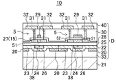
- FIG. 1 is a cross-sectional view showing the main part of the semiconductor device according to the first embodiment.
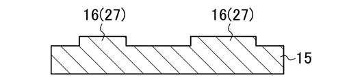
- FIG. 2 is a cross-sectional view showing a base layer on which a convex region is formed in the first embodiment.
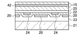
- FIG. 3 is a cross-sectional view showing a state where hydrogen ions are implanted into the base layer on which the first insulating film is formed in the first embodiment.
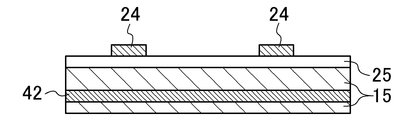
- FIG. 4 is a cross-sectional view showing a base layer on which a release layer and a light-shielding film are formed according to Embodiment 1.
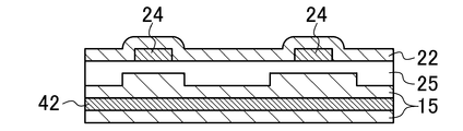
- FIG. 5 is a cross-sectional view showing the base layer on which the second insulating film covering the light shielding film in Embodiment 1 is formed.
- FIG. 1 is a cross-sectional view showing the main part of the semiconductor device according to the first embodiment.
- FIG. 2 is a cross-sectional view showing a base layer on which a convex region is formed in the first embodiment.
- FIG. 3 is a cross
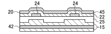
- FIG. 6 is a cross-sectional view showing the silicon oxide film formed on the second insulating film in the first embodiment.
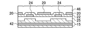
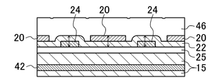
- FIG. 7 is a cross-sectional view showing an insulating material layer covering the dummy pattern in the first embodiment.
- FIG. 8 is a cross-sectional view showing the base layer on which the third insulating film is formed in the first embodiment.
- FIG. 9 is a cross-sectional view showing the base layer attached to the glass substrate in the first embodiment.
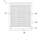
- FIG. 10 is a plan view schematically showing the main part of the liquid crystal display device.
- FIG. 11 is a cross-sectional view showing the main part of the semiconductor device according to the second embodiment.
- FIG. 12 is a cross-sectional view showing a base layer on which a release layer is formed in the second embodiment.
- FIG. 13 is a cross-sectional view showing a base layer on which a light-shielding film in Embodiment 2 is formed.
- FIG. 14 is a cross-sectional view showing a base layer on which a second insulating film covering the light shielding film in the second embodiment is formed.
- FIG. 15 is a cross-sectional view showing a silicon oxide film formed on the second insulating film in the second embodiment.
- FIG. 16 is a cross-sectional view showing an insulating material layer covering the dummy pattern in the second embodiment.
- FIG. 17 is a cross-sectional view showing the base layer on which the third insulating film is formed in the second embodiment.
- FIG. 18 is a cross-sectional view showing a base layer bonded to a glass substrate.
- FIG. 19 is a cross-sectional view showing a base layer on which a semiconductor layer is formed in the second embodiment.
- FIG. 20 is a cross-sectional view showing the main part of the semiconductor device according to the third embodiment.
- FIG. 21 is a graph showing the relationship between the voltage and the capacitance in the first capacitive element and the second capacitive element in the third embodiment.
- FIG. 22 is a cross-sectional view showing a main part of a conventional semiconductor device.
- FIG. 23 is a cross-sectional view showing an insulating layer covering a light shielding film formed on a conventional support substrate.
- FIG. 24 is a cross-sectional view showing a conventional support substrate on which a light shielding film is formed and a silicon substrate facing the support substrate.
- FIG. 25 is a cross-sectional view showing a silicon layer thinned on a conventional support substrate.
- FIG. 26 is a cross-sectional view showing a back gate insulating film and a conductive material layer formed in an opening of a conventional insulating film.
- FIG. 27 is a cross-sectional view showing a conventional interlayer insulating film covering a recessed back gate electrode.
- Embodiment 1 of the Invention 1 to 10 show Embodiment 1 of the present invention.
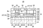
- FIG. 1 is a cross-sectional view showing a main part of the semiconductor device 10 according to the first embodiment.
- FIG. 10 is a plan view schematically showing the main part of the liquid crystal display device 1.
- the liquid crystal display device 1 includes a TFT substrate 11, a counter substrate 12 disposed to face the TFT substrate 11, and a liquid crystal layer provided between the TFT substrate 11 and the counter substrate 12. (Not shown).
- the liquid crystal display device 1 has a display region 17 in a region where the TFT substrate 11 and the counter substrate 12 overlap each other.
- a plurality of pixels 19 are arranged in a matrix in the display area 17.
- the TFT substrate 11 is composed of a glass substrate 21 as a transparent support substrate, and has a circuit region 18 in a region not overlapping the counter substrate 12.
- a circuit such as a driver for driving and controlling each pixel 19 is directly formed on the glass substrate 21 constituting the TFT substrate 11.
- the driver in the circuit area 18 has a TFT 5 described later.
- the TFT substrate 11 is provided with a TFT as a switching element and a pixel electrode connected thereto for each pixel 19. Furthermore, a gate wiring and a source wiring are connected to the TFT. The ends of the gate wiring and source wiring are drawn out to the circuit region 18 and connected to the driver or the like.
- the counter substrate 12 is made of a glass substrate as a transparent support substrate, and a color filter, a common electrode, and the like are formed on the surface on the TFT substrate 11 side.
- a backlight (not shown) as a light source is provided on the opposite side of the TFT substrate 11 from the counter substrate 12.
- the semiconductor device 10 is applied as various functional circuits such as a driver directly formed on the glass substrate 21 constituting the TFT substrate 11.
- the semiconductor device 10 includes a glass substrate 21 that is a support substrate, and a device portion D that is formed on the glass substrate 21 with high density and high accuracy.
- the support substrate 21 is preferably a transparent substrate such as a glass substrate 21, but when applied to other display devices or the like, a single crystal is used.
- Other substrates such as a silicon semiconductor substrate can be applied to the support substrate.
- the device portion D includes a third insulating film 33 attached to the flat surface of the glass substrate 21 by self-bonding, a TFT 5 that is a semiconductor element formed on the third insulating film 33, and the TFT 5 and the glass substrate 21. And a light shielding film 24 disposed between the two.
- the TFT 5 is composed of, for example, a PMOS transistor.
- a light shielding film 24 or a back gate electrode can be formed between the TFT 5 and the glass substrate 21.
- the light shielding film 24 is formed in FIG. 1, two TFTs 5 are shown, but the device to be formed is not limited to this.
- the present invention can be similarly applied not only to the NMOS transistor but also to other elements such as a bipolar transistor, a capacitor element described later, or a diode. Further, the number is not particularly limited.
- a plurality of first recesses 23 and second recesses 26 are alternately formed on the surface of the third insulating film 33 opposite to the glass substrate 21.
- dummy patterns 20 made of, for example, a silicon oxide film are provided in the first recess 23.
- a second insulating film 22 is formed on the surface of the third insulating film 33 so as to cover each dummy pattern 20. That is, a part of the second insulating film 22 is provided in the second recess 26.
- the second insulating film 22 has a substantially constant thickness. Therefore, when the second insulating film 22 is formed along the second concave portion 26, a third concave portion 38 is formed in a region of the second insulating film 22 that overlaps the second concave portion 26.
- the second insulating film 22 is composed of a protective insulating film that suppresses transmission of metal ions. That is, the second insulating film 22 is constituted by a dense insulating film such as a silicon nitride film.
- the total thickness of the dummy pattern 20 and the second insulating film 22 overlapping the dummy pattern 20 is the same as the total thickness of the light shielding film 24 and the second insulating film 22 overlapping the light shielding film 24. It has become.
- the third insulating film 33 has a thickness from the flat surface of the glass substrate 21 such that the dummy pattern 20 in the first recess 23 is provided and the second insulating film 22 in the second recess 26. Are the same in the region in which is provided.
- the light shielding film 24 is provided in the third recess 38.
- the surface of the light shielding film 24 forms the same plane as the surface of the second insulating film 22.
- the light shielding film 24 is made of a refractory metal such as Mo, TiN, or W, for example.
- the light shielding film 24 may be configured to function also as a back gate electrode. In this case, the characteristics of the TFT 5 can be dynamically changed by adjusting the potential of the back gate electrode.
- the first insulating film 25 is formed on the surface of the second insulating film 22 so as to cover the light shielding film 24.
- a fourth recess 39 is formed in a region overlapping with at least a part of the light shielding film 24.
- the semiconductor layer 27 is formed in the fourth recess 39, and the surface of the semiconductor layer 27 constitutes the same plane as the surface of the first insulating film 25 opposite to the second insulating film 22. As a result, the semiconductor layer 27 is formed in an island shape on the surface of the first insulating film 25. Further, at least a part of the semiconductor layer 27 overlaps the light shielding film 24. It is preferable that at least the channel region 51 in the semiconductor layer 27 overlaps the light shielding film 24.
- the semiconductor layer 27 has a channel region 51 and high-concentration impurity regions 52 formed on both the left and right sides thereof.
- the semiconductor layer 27 is also referred to as a base layer.
- the base layer 15 is made of, for example, a single crystal silicon semiconductor layer.
- the base layer 15 includes a group IV semiconductor, a group II-VI compound semiconductor, a group III-V compound semiconductor, a group IV-IV compound semiconductor, and a mixed crystal containing these homologous elements, In addition, at least one selected from the group consisting of oxide semiconductors can be included.
- a part of the base layer 15 is separated and removed along a peeling layer 42 formed by ion implantation of a peeling material such as hydrogen.
- a part of the base layer 15 is thinned by being removed by heat treatment.
- the surfaces of the semiconductor layer 27 and the first insulating film 25 are directly covered with the gate insulating film 28.
- a gate electrode 29 is formed on the surface of the gate insulating film 28 so as to overlap the channel region 51 of the semiconductor layer 27.
- An interlayer insulating film 30 is formed on the gate insulating film 28 so as to cover the gate electrode 29.
- a contact hole 31 is formed through the interlayer insulating film 30 above the high concentration impurity region 52 of the semiconductor layer 27.
- wiring portions (that is, source wirings and drain wirings) 32 are formed on the surface of the interlayer insulating film 30 and inside the contact holes 31.
- a protective film 40 is formed on the surface of the interlayer insulating film 30 so as to cover each wiring part 32.
- FIG. 2 is a cross-sectional view showing the base layer 15 on which the convex regions 16 are formed.
- FIG. 3 is a cross-sectional view showing a state where hydrogen ions are implanted into the base layer 15 on which the first insulating film 25 is formed.
- FIG. 4 is a cross-sectional view showing the base layer 15 on which the release layer 42 and the light shielding film 24 are formed.
- FIG. 5 is a cross-sectional view showing the base layer 15 on which the second insulating film 22 covering the light shielding film 24 is formed.
- FIG. 6 is a cross-sectional view showing the silicon oxide film 45 formed on the second insulating film 22.
- FIG. 7 is a cross-sectional view showing an insulating material layer 46 covering the dummy pattern 20.
- FIG. 8 is a cross-sectional view showing the base layer 15 on which the third insulating film 33 is formed.
- FIG. 9 is a cross-sectional view showing the base layer 15 attached to the glass substrate 21.
- the convex region 16 to be the semiconductor layer 27 is formed by etching the surface of the silicon wafer 15 that is the base layer 15.
- the base layer 15 is a single crystal silicon layer.
- a first insulating film 25 having a flat surface is formed on the surface of the base layer 15. That is, after forming an insulating film so as to cover the convex region 16, the surface of the insulating film is planarized by CMP or the like.
- a release material 41 is ion-implanted into the base layer 15 on which the first insulating film 25 is formed to form a release layer 42.
- hydrogen is applied to the peeling material 41.
- an inert element such as He or Ne can be used instead of hydrogen. It is also possible to apply hydrogen and inert elements.
- the peeling layer 42 can be formed at a substantially constant depth inside the base layer 15.
- a plurality of light shielding films 24 are formed on the surface of the first insulating film 25. That is, after a refractory metal layer such as Mo, TiN or W is formed on the surface of the first insulating film 25, the light shielding film 24 is formed by etching the metal layer by photolithography. In this step, the light shielding film 24 is formed so as to overlap at least a part of the convex region 16. If a back gate electrode is formed instead of the light shielding film 24, it is formed in the same manner in this step.
- a second insulating film 22 that covers the light shielding film 24 and has an uneven surface reflecting the step shape of the light shielding film 24 is formed on the surface of the first insulating film 25.
- the second insulating film 22 is a dense protective insulating film such as a silicon nitride film. The second insulating film 22 suppresses transmission of metal ions.
- the dummy pattern 20 is formed on the surface of the second insulating film 22 between the adjacent light shielding films 24. That is, as shown in FIG. 6, a silicon oxide film 45 as an insulating film is formed on the entire surface of the second insulating film 22. The thickness of the silicon oxide film 45 is approximately the same as that of the light shielding film 24.
- the dummy pattern 20 is formed as shown in FIG. 7 by etching the silicon oxide film 45 formed on the surface of the second insulating film 22 using the second insulating film 22 as an etch stopper. Accordingly, the height of the dummy pattern 20 is the same as the surface height of the second insulating film 22 on the light shielding film 24 with reference to the surface of the first insulating film 25 on the second insulating film 22 side.
- a third insulating film 33 that covers the dummy pattern 20 and has a flat surface is formed on the surface of the second insulating film 22.
- an insulating material layer 46 is formed on the surface of the second insulating film 22.
- the distance between the light shielding film 24 and the dummy pattern 20 (the distance in the direction parallel to the surface of the glass substrate 21) is larger than the thickness of the second insulating film 22, and the insulating material layer 46 on the light shielding film 24. It is smaller than the thickness. This makes it difficult to form a large depression on the surface of the insulating material layer 46 on the region between the dummy pattern 20 and the light shielding film 24.
- the surface of the insulating material layer 46 is polished and planarized by a CMP method or the like, thereby forming a third insulating film 33.
- the base layer 15 provided with the third insulating film 33 and a part of the device portion D is formed on the glass substrate as a supporting substrate on the flat surface of the third insulating film 33.
- the surface of the second insulating film 22 is attached to the surface of the glass substrate 21 by self-bonding by van der Waals force.
- a gate insulating film 28 is formed so as to cover the semiconductor layer 27.
- the surface of the gate insulating film 28 is formed flat along the surfaces of the semiconductor layer 27 and the first insulating film 25.
- the gate electrode 29 is formed on the surface of the gate insulating film 28 so as to overlap the channel region 51 of the semiconductor layer 27.
- an impurity element is introduced into at least a part of the semiconductor layer 27 to form a high concentration impurity region 52.
- the impurity element is introduced into the semiconductor layer 27 using the gate electrode 29 as a mask.
- a high concentration impurity region 52 is formed in a region that does not overlap with the gate electrode 29, while a channel region 51 is formed in a region that overlaps with the gate electrode 29.
- contact holes 31 are formed in the interlayer insulating film 30 and the like.
- the metal layer formed on the interlayer insulating film 30 is patterned by photolithography to form a plurality of wiring portions 32.
- the semiconductor device 10 is manufactured by performing the above steps.
- 20 is formed, on the flat surface of the first insulating film, the total thickness of the dummy pattern 20 and the second insulating film 22 overlapping the dummy pattern 20, the light shielding film 24 and the light shielding film
- the total thickness of the second insulating film 22 overlapping the film 24 can be made the same.
- the third insulating film 33 covering the light shielding film 24 can be planarized on the base layer 15 with high accuracy by the CMP method. Therefore, the subsequent bonding process to the glass substrate 21 can be easily performed. Further, it is not necessary to perform the CMP process on the large glass substrate 21.
- the light shielding film 24 is covered by making the distance between the light shielding film 24 and the dummy pattern 20 larger than the thickness of the second insulating film 22 and smaller than the thickness of the insulating material layer 46 on the light shielding film 24.
- the dummy pattern 20 can be formed so as not to run over the inclined second insulating film 22, and a large depression is formed on the surface of the insulating material layer 46 on the region between the dummy pattern 20 and the light shielding film 24. It becomes difficult to be done. Therefore, the surface of the insulating material layer 46 can be easily and accurately planarized.
- the dummy pattern 20 is formed after the second insulating film 22 composed of a dense protective insulating film such as a silicon nitride film is formed, even when the supporting substrate is the glass substrate 21, the glass substrate By suppressing the transmission of metal ions (movable ions) from the 21 side, fluctuations in the characteristics of the TFT 5 that is a semiconductor element can be prevented.
- the second insulating film 22 can be used as an etch stopper, the dummy pattern 20 can be formed more easily and accurately while preventing the lower layer of the light shielding film 24 and the like from being eroded.
- the dummy pattern 20 is formed of a silicon oxide film, an unnecessary increase in load capacity can be prevented and a decrease in the aperture ratio of the liquid crystal display device 1 can be suppressed as compared with the case where the dummy pattern 20 is formed of a metal film. .
- the peeling material 41 can be ion-implanted into the base layer 15 before the light shielding film 24 is formed, the ion implantation depth in the base layer 15 is made uniform, and the peeling layer 42 is formed at a certain depth position. be able to.
- the light-shielding film 24 is formed in advance on the base layer 15 before the base layer 15 is attached to the glass substrate 21, the light-shielding film and the semiconductor layer in the pasting process to the glass substrate as in the prior art.
- the desired region of the semiconductor layer 27 can be more easily covered with the light-shielding film 24 while eliminating the need for highly accurate alignment.
- the semiconductor layer 27 can be easily formed flat by being bonded to the glass substrate 21. Further, since the semiconductor layer 27 is not formed in a step shape, the gate insulating film 28 can be easily thinned. As a result, the threshold voltage in the semiconductor layer 27 can be controlled with high accuracy, and the power consumption of the semiconductor device 10 can be reduced.
- the semiconductor layer 27 is made of single crystal silicon, it is possible to prevent the occurrence of leakage current due to crystal defects. As a result, the characteristics of the TFT 5 having the semiconductor layer 27 can be greatly improved.
- Embodiment 2 of the Invention >> 11 to 19 show Embodiment 2 of the present invention.
- FIG. 11 is a cross-sectional view showing a main part of the semiconductor device 10 according to the second embodiment.
- the same parts as those in FIGS. 1 to 10 are denoted by the same reference numerals, and detailed description thereof will be omitted.
- the semiconductor layer 27 is formed in the fourth recess 39 formed in the first insulating film 25, whereas in the second embodiment, the semiconductor layer 27 is formed on the flat first insulating film 25. It is to be formed.
- the total thickness of the dummy pattern 20 and the second insulating film 22 overlapping the dummy pattern 20 is the second overlapping the light shielding film 24 and the light shielding film 24.
- the total thickness with the insulating film 22 is the same.
- the surfaces of the first insulating film 25 provided on the surfaces of the light shielding film 24 and the second insulating film 22 are formed flat.
- a semiconductor layer 27 is formed in an island shape on the surface of the flat first insulating film 25.
- the surface of the gate insulating film 28 covering the semiconductor layer 27 is formed in a convex shape in the region covering the semiconductor layer 27.
- FIG. 12 is a cross-sectional view showing the base layer 15 on which the release layer 42 is formed.
- FIG. 13 is a cross-sectional view showing the base layer 15 on which the light shielding film 24 is formed.
- FIG. 14 is a cross-sectional view showing the base layer 15 on which the second insulating film 22 covering the light shielding film 24 is formed.
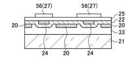
- FIG. 15 is a cross-sectional view showing the silicon oxide film 45 formed on the second insulating film 22.
- FIG. 16 is a cross-sectional view showing an insulating material layer 46 covering the dummy pattern 20.
- FIG. 17 is a cross-sectional view showing the base layer 15 on which the third insulating film 33 is formed.
- FIG. 18 is a cross-sectional view showing the base layer 15 attached to the glass substrate 21.
- FIG. 19 is a cross-sectional view showing the base layer 15 on which the semiconductor layer 27 is formed.
- the first insulating film 25 is formed on the surface of the silicon wafer 15 that is the base layer 15. Since the surface of the base layer 15 is flat, the surface of the first insulating film 25 is also formed flat.
- a release material 41 is ion-implanted into the base layer 15 on which the first insulating film 25 is formed to form a release layer 42.
- hydrogen or an inert element He, Ne, or the like
- the peeling layer 42 can be formed at a substantially constant depth inside the base layer 15.
- a light shielding film 24 is formed on the surface of the first insulating film 25. That is, after a refractory metal layer such as Mo, TiN or W is formed on the surface of the first insulating film 25, the light shielding film 24 is formed by etching the metal layer by photolithography.
- a refractory metal layer such as Mo, TiN or W
- a second insulating film 22 that covers the light shielding film 24 and has an uneven surface reflecting the step shape of the light shielding film 24 is formed on the surface of the first insulating film 25.
- the second insulating film 22 is a dense protective insulating film such as a silicon nitride film.
- the dummy pattern 20 is formed on the surface of the second insulating film 22 between the adjacent light shielding films 24. That is, as shown in FIG. 15, a silicon oxide film 45 as an insulating film is formed on the entire surface of the second insulating film 22. The thickness of the silicon oxide film 45 is approximately the same as that of the light shielding film 24.
- the silicon oxide film 45 formed on the surface of the second insulating film 22 is etched to form a dummy pattern 20 as shown in FIG.
- an insulating material layer 46 is formed on the surface of the second insulating film 22. Thereafter, as shown in FIG. 17, the surface of the insulating material layer 46 is polished and planarized by a CMP method or the like, thereby forming the third insulating film 33.
- the base layer 15 provided with the light shielding film 24 is attached to the glass substrate 21 on the flat surface of the third insulating film 33.
- the surface of the third insulating film 33 is attached to the surface of the glass substrate 21 by self-bonding by van der Waals force.
- the base layer 15 remaining on the glass substrate 21 is etched to form a convex region 56 to be the semiconductor layer 27 so as to overlap at least a part of the light shielding film 24.
- the convex region 56 is formed in an island shape as shown in FIG.
- a gate insulating film 28 is formed so as to cover the semiconductor layer 27.
- the surface of the gate insulating film 28 is formed in a convex shape along the surface of the semiconductor layer 27.
- a gate electrode 29 is formed on the surface of the gate insulating film 28 so as to overlap the channel region 51 of the semiconductor layer 27.
- contact holes 31 are formed in the interlayer insulating film 30 and the like, and a plurality of wiring portions 32 are formed.
- the semiconductor device 10 is manufactured by performing the above steps.
- Embodiment 2- Therefore, according to the second embodiment, as in the first embodiment, it is not necessary to perform the CMP process on the large-sized glass substrate 21, and the third insulation covering the light shielding film 24 regardless of the shape of the light shielding film 24.
- the film 33 can be planarized on the base layer 15 with high accuracy by the CMP method.
- the base layer 15 is formed through the base layer 15 and the first insulating film 25 having a flat surface. Hydrogen can be ion implanted. As a result, the release layer 42 can be formed at a more uniform depth position.
- the planarization process of the first insulating film 25 becomes unnecessary, the planarization process by the CMP method can be reduced, and the planarization process can be performed only once when the third insulating film 33 is formed. can do.
- FIG. 20 shows Embodiment 3 of the present invention.
- FIG. 20 is a cross-sectional view showing a main part of the semiconductor device 10 according to the third embodiment.
- FIG. 21 is a graph showing the relationship between the voltage and the capacitance in the first capacitive element 6a and the second capacitive element 6b.
- the semiconductor device 10 has the TFT 5 as a semiconductor element, whereas at least one of the semiconductor elements included in the semiconductor device 10 in the third embodiment is the capacitive elements 6a and 6b. is there.
- the semiconductor device 10 in this embodiment includes a glass substrate 21 as a support substrate and a device portion D formed on the glass substrate 21 with high density and high accuracy.
- the device portion D includes a first capacitor element 6a and a second capacitor element 6b.
- the first capacitive element 6a is a semiconductor into which a back gate electrode 54 serving as one capacitive electrode and an N + type impurity element serving as the other capacitive electrode disposed so as to be opposed thereto are introduced.
- a layer 27 high-concentration impurity region 52).
- the second capacitive element 6b has a semiconductor layer 27 (channel region 51 and high-concentration impurity region 52) as one capacitive electrode, and an electrode layer 55 as the other capacitive electrode arranged opposite to the semiconductor layer 27. ing.
- first recesses 23 and second recesses 26 are alternately formed on the flat surface of the glass substrate 21.
- first recess 23 dummy patterns 20 made of, for example, a silicon oxide film are provided.
- a second insulating film 22 is formed on the surface of the third insulating film 33 so as to cover each dummy pattern 20. That is, a part of the second insulating film 22 is provided in the second recess 26.
- the second insulating film 22 has a substantially constant thickness. Therefore, when the second insulating film 22 is formed along the second concave portion 26, a third concave portion 38 is formed in a region of the second insulating film 22 that overlaps the second concave portion 26.
- the second insulating film 22 is composed of a dense insulating film such as a silicon nitride film.
- the total thickness of the dummy pattern 20 and the second insulating film 22 overlapping the dummy pattern 20 is the light shielding film 24 and the light shielding film 24. This is the same as the total thickness of the second insulating film 22 that overlaps with the second insulating film 22.
- the back gate electrode 54 or the light shielding film 24 is provided in the third recess 38.
- the surfaces of the back gate electrode 54 and the light shielding film 24 constitute the same plane as the surface of the second insulating film 22.
- the back gate electrode 54 and the light shielding film 24 are made of a refractory metal such as Mo, TiN, or W, for example.
- the first insulating film 25 is formed on the surface of the second insulating film 22 so as to cover the back gate electrode 54 and the light shielding film 24.
- a fourth recess 39 is formed in a region overlapping with at least part of the back gate electrode 54 and the light shielding film 24. Further, at least a part of the semiconductor layer 27 overlaps the back gate electrode 54 or the light shielding film 24.
- the semiconductor layer 27 is formed in the fourth recess 39, and the surface of the semiconductor layer 27 constitutes the same plane as the surface of the first insulating film 25 opposite to the second insulating film 22. As a result, the semiconductor layer 27 is formed in an island shape on the surface of the first insulating film 25.
- a high concentration impurity region 52 constituting the first capacitor element 6a is provided in the fourth recess 39 facing the back gate electrode 54.
- a channel region 51 and a high-concentration impurity region 52 constituting the second capacitor element 6b are provided in the fourth recess 39 facing the light shielding film 24 in the fourth recess 39 facing the light shielding film 24 in the fourth recess 39 facing the light shielding film 24 in the fourth recess 39 facing the light shielding film 24, a channel region 51 and a high-concentration impurity region 52 constituting the second capacitor element 6b are provided.
- a part of the base layer 15 is separated and removed along a release layer 42 formed by ion implantation of a release material such as hydrogen.
- a part of the base layer 15 is thinned by being removed by heat treatment.
- the surfaces of the semiconductor layers 27 and the first insulating film 25 are directly covered with the gate insulating film 28.
- An electrode layer 55 is formed on the surface of the gate insulating film 28 so as to overlap the channel region 51 of the semiconductor layer 27 constituting the second capacitive element 6b.
- An interlayer insulating film 30 is formed on the gate insulating film 28 so as to cover the electrode layer 55.
- a contact hole 31 is formed through the interlayer insulating film 30 above the electrode layer 55, the back gate electrode 54, and the high-concentration impurity regions 52. Further, a wiring portion 32 is formed on the surface of the interlayer insulating film 30 and inside the contact hole 31.
- a protective film 40 is formed on the surface of the interlayer insulating film 30 so as to cover each wiring part 32.
- the semiconductor device 10 of this embodiment can be manufactured in the same manner as in the first embodiment. Then, as at least one of the semiconductor elements, a semiconductor layer (high-concentration impurity region 52) into which an impurity element is introduced and the back gate electrode 54 are formed so as to face each other. A capacitive element 6a having the back gate electrode 54 as a pair of capacitive electrodes is formed.
- the convex region forming step, the first insulating film forming step, and the release layer forming step are sequentially performed.
- the light shielding film forming step the light shielding film 24 and the back gate electrode 54 are formed simultaneously.
- the back gate electrode 54 is formed by patterning a refractory metal layer by photolithography and etching.
- a second insulating film forming process, a dummy pattern forming process, a third insulating film forming process, an attaching process, a separating process, a semiconductor layer forming process, and a gate insulating film forming process are sequentially performed.
- the semiconductor layer forming step the semiconductor layer 27 that forms the capacitor electrodes of the first capacitor element 6a and the second capacitor element 6b is formed.
- the electrode layer 55 is formed at a position overlapping the channel region 51 as in the gate electrode forming step.
- a contact hole 31 is formed in the interlayer insulating film 30 or the like.
- the metal layer formed on the interlayer insulating film 30 is patterned by photolithography to form a plurality of wiring portions 32.
- the semiconductor device 10 is manufactured by performing the above steps.
- the back gate electrode 54 and the light shielding film 24 can be used regardless of the shapes of the back gate electrode 54 and the light shielding film 24.
- 54 and the third insulating film 33 covering the light shielding film 24 can be planarized on the base layer 15 with high accuracy by the CMP method.
- the light shielding film 24 that overlaps the channel region 51 of the semiconductor layer 27 is provided for the second capacitor element 6b, it is possible to prevent light from entering the channel region 51 and prevent malfunction.
- the second capacitor element 6b since one of the capacitor electrodes is the channel region 51 of the semiconductor layer 27, a capacitor C is generated by an applied voltage equal to or higher than the threshold voltage.
- the first capacitor element 6a one of the capacitor electrodes is entirely constituted by the high-concentration impurity region 52 of the semiconductor layer 27. Therefore, the capacitor C is constant regardless of the applied voltage. That is, the first capacitive element 6a can be used as a stable capacitive element in a wide applied voltage region.
- each pixel 19 The present invention can also be applied to a semiconductor device having a TFT for forming a TFT and driving a pixel electrode.
- the present invention can be similarly applied to semiconductor devices used for other display devices such as an organic EL display device.
- the present invention is useful for a semiconductor device used in, for example, a liquid crystal display device and a manufacturing method thereof.
- Liquid crystal display device 5 TFT (semiconductor element) 6a First capacitor element 6b Second capacitor element 10 Semiconductor devices 15 Base layer 16 Convex area 20 dummy pattern 21 Glass substrate, support substrate 22 Second insulating film (protective insulating film) 23 First recess 24 Shading film 25 First insulating film 26 Second recess 27 Semiconductor layer 33 Third insulating film 38 Third recess 41 Release material 42 Release layer 46 Insulation layer 51 channel region 52 High concentration impurity region 54 Back gate electrode 56 Convex area
Landscapes
- Physics & Mathematics (AREA)
- Nonlinear Science (AREA)
- Engineering & Computer Science (AREA)
- Microelectronics & Electronic Packaging (AREA)
- Mathematical Physics (AREA)
- Chemical & Material Sciences (AREA)
- Crystallography & Structural Chemistry (AREA)
- General Physics & Mathematics (AREA)
- Optics & Photonics (AREA)
- Power Engineering (AREA)
- Thin Film Transistor (AREA)
- Liquid Crystal (AREA)
Abstract
Description
次に、本発明の作用について説明する。
図1~図10は、本発明の実施形態1を示している。
液晶表示装置1は、図10に示すように、TFT基板11と、このTFT基板11に対向して配置された対向基板12と、これらTFT基板11及び対向基板12の間に設けられた液晶層(図示省略)とを備えている。
本実施形態における半導体装置10は、上記TFT基板11を構成するガラス基板21に直接に形成されたドライバ等の各種機能回路として適用されている。図1に示すように、半導体装置10は、支持基板であるガラス基板21と、ガラス基板21上に高密度且つ高精度に形成されたデバイス部Dとを備えている。
次に、上記半導体装置10の製造方法について、図1~図9を参照して説明する。
まず、図2に示すように、基体層15であるシリコンウェハ15の表面をエッチングすることにより、半導体層27となる凸状領域16を形成する。ここで、基体層15は、単結晶シリコン層である。
次に、図3に示すように、基体層15の表面に平坦な表面を有する第1絶縁膜25を形成する。すなわち、凸状領域16を覆うように絶縁膜を形成した後に、当該絶縁膜の表面をCMP等によって平坦化する。
次に、図3及び図4に示すように、第1絶縁膜25を形成した基体層15に剥離用物質41をイオン注入して剥離層42を形成する。剥離用物質41には、例えば水素を適用する。尚、水素の代わりに、HeやNe等の不活性元素を適用することが可能である。また、水素及び不活性元素を適用することも可能である。本実施形態では、第1絶縁膜25の表面が平坦化されているので、剥離層42を基体層15の内部で略一定の深さに形成することができる。
次に、図4に示すように、第1絶縁膜25の表面に複数の遮光膜24を形成する。すなわち、第1絶縁膜25の表面に、例えばMo、TiN又はW等の高融点金属層を形成した後に、当該金属層をフォトリソグラフィによりエッチングして遮光膜24を形成する。この工程では、上記凸状領域16の少なくとも一部に重なるように、遮光膜24を形成する。尚、遮光膜24の代わりにバックゲート電極を形成する場合には、この工程で同様にして形成する。
次に、図5に示すように、遮光膜24を覆うと共に、当該遮光膜24の段差形状を反映した凹凸状の表面を有する第2絶縁膜22を、第1絶縁膜25の表面に形成する。第2絶縁膜22は、例えばシリコン窒化膜等の緻密な保護絶縁膜である。この第2絶縁膜22は、金属イオンの透過を抑制する。
次に、図7に示すように、隣り合う遮光膜24同士の間における第2絶縁膜22の表面にダミーパターン20を形成する。すなわち、図6に示すように、第2絶縁膜22の表面全体に絶縁膜としてのシリコン酸化膜45を形成する。このシリコン酸化膜45の厚みは、遮光膜24と同程度とする。
次に、図8に示すように、第2絶縁膜22の表面に、ダミーパターン20を覆うと共に平坦な表面を有する第3絶縁膜33を形成する。まず、図7に示すように、第2絶縁膜22の表面に絶縁材層46を形成する。
次に、図9に示すように、第3絶縁膜33が設けられてデバイス部Dの一部が形成された基体層15を、第3絶縁膜33の平坦な表面において支持基板としてのガラス基板21に貼り付ける。このとき、第2絶縁膜22の表面は、ファンデルワールス力による自己接合によって、ガラス基板21の表面に貼り付けられる。
次に、ガラス基板21に貼り付けられた基体層15の一部を、剥離層42に沿って分離除去する。すなわち、ガラス基板21に貼り付けられた基体層15を400~600℃程度に加熱することによって、基体層15における剥離層42を介してガラス基板21とは反対側の一部分を、剥離層42に沿って分離除去する。
次に、凸状領域16の周囲の第1絶縁膜25をエッチストッパとして、ガラス基板21上に残った基体層15をエッチングし、半導体素子としてのTFT5を構成する半導体層27を形成する。このとき、半導体層27の少なくとも一部が遮光膜24に重なるように形成される。その結果、基体層15の凸状領域16であった部分のみがアイランド状に残って半導体層27となる。
次に、図1に示すように、半導体層27を覆うように、ゲート絶縁膜28を形成する。ゲート絶縁膜28の表面は、半導体層27及び第1絶縁膜25の表面に沿って平坦に形成される。
次に、図1に示すように、ゲート絶縁膜28の表面に、半導体層27のチャネル領域51に重なるようにゲート電極29を形成する。
次に、図1に示すように、半導体層27の少なくとも一部に不純物元素を導入して高濃度不純物領域52を形成する。不純物元素は、ゲート電極29をマスクとして半導体層27に導入する。その結果、ゲート電極29に重ならない領域に高濃度不純物領域52が形成される一方、ゲート電極29に重なっている領域にチャネル領域51が形成される。
したがって、この実施形態1によると、第2絶縁膜22の表面に、第1絶縁膜25の表面からの高さが、遮光膜24上の第2絶縁膜22の表面高さと同じであるダミーパターン20を形成するようにしたので、第1絶縁膜の平坦な表面上において、ダミーパターン20と当該ダミーパターン20に重なっている第2絶縁膜22との厚みの合計と、遮光膜24と当該遮光膜24に重なっている第2絶縁膜22との厚みの合計とを、互いに同じにすることができる。その結果、遮光膜24の形状にかかわらず、当該遮光膜24を覆う第3絶縁膜33を基体層15上で高精度にCMP法によって平坦化することができる。したがって、後のガラス基板21への貼り合わせ工程も容易に行うことができる。また、大判のガラス基板21上でCMP処理を行う必要もない。
図11~図19は、本発明の実施形態2を示している。
半導体装置10は、上記実施形態1と同様に、ダミーパターン20と、ダミーパターン20に重なっている第2絶縁膜22との厚みの合計は、遮光膜24と遮光膜24に重なっている第2絶縁膜22との厚みの合計と、同じになっている。
次に、上記半導体装置10の製造方法について、図12~図19を参照して説明する。
まず、図12に示すように、基体層15であるシリコンウェハ15の表面に第1絶縁膜25を形成する。基体層15の表面は平坦であるので、第1絶縁膜25の表面も平坦に形成される。
次に、図12に示すように、第1絶縁膜25を形成した基体層15に剥離用物質41をイオン注入して剥離層42を形成する。剥離用物質41には、上記実施形態1と同様に、水素又は不活性元素(HeやNe等)を適用する。第1絶縁膜25の表面が平坦であるため、剥離層42を基体層15の内部で略一定の深さに形成することができる。
次に、図13に示すように、第1絶縁膜25の表面に遮光膜24を形成する。すなわち、第1絶縁膜25の表面に、例えばMo、TiN又はW等の高融点金属層を形成した後に、当該金属層をフォトリソグラフィによりエッチングして遮光膜24を形成する。
次に、図14に示すように、遮光膜24を覆うと共に、当該遮光膜24の段差形状を反映した凹凸状の表面を有する第2絶縁膜22を、第1絶縁膜25の表面に形成する。第2絶縁膜22は、例えばシリコン窒化膜等の緻密な保護絶縁膜である。
次に、図16に示すように、隣り合う遮光膜24同士の間における第2絶縁膜22の表面にダミーパターン20を形成する。すなわち、図15に示すように、第2絶縁膜22の表面全体に絶縁膜としてのシリコン酸化膜45を形成する。このシリコン酸化膜45の厚みは、遮光膜24と同程度とする。
次に、図16に示すように、第2絶縁膜22の表面に絶縁材層46を形成する。その後、図17に示すように、絶縁材層46の表面をCMP法等により研磨して平坦化することにより、第3絶縁膜33を形成する。
次に、図18に示すように、遮光膜24が設けられている基体層15を、第3絶縁膜33の平坦な表面においてガラス基板21に貼り付ける。このとき、第3絶縁膜33の表面は、ファンデルワールス力による自己接合によって、ガラス基板21の表面に貼り付けられる。
次に、ガラス基板21に貼り付けられた基体層15の一部を、400~600℃程度に加熱することにより、剥離層42に沿って分離除去する。
次に、図19に示すように、ガラス基板21上に残った基体層15をエッチングすることにより、半導体層27となる凸状領域56を、遮光膜24の少なくとも一部に重なるように形成する。この凸状領域56は、図19に示すように、アイランド状に形成される。
次に、図11に示すように、半導体層27を覆うように、ゲート絶縁膜28を形成する。ゲート絶縁膜28の表面は、半導体層27の表面に沿って凸面状に形成される。
次に、図11に示すように、ゲート絶縁膜28の表面に、半導体層27のチャネル領域51に重なるようにゲート電極29を形成する。
次に、図11に示すように、ゲート電極29をマスクとして、不純物元素を半導体層27に導入する。そのことにより、ゲート電極29に重ならない領域に高濃度不純物領域52を形成する一方、ゲート電極29に重なっている領域にチャネル領域51を形成する。
したがって、この実施形態2によると、上記実施形態1と同様に、大判のガラス基板21上でCMP処理を行う必要がなく、遮光膜24の形状にかかわらず、当該遮光膜24を覆う第3絶縁膜33を、基体層15上で高精度にCMP法により平坦化することができる。
図20は、本発明の実施形態3を示している。
上記実施形態1及び2では、半導体装置10が半導体素子としてのTFT5を有していたのに対し、本実施形態3における半導体装置10が有する半導体素子の少なくとも1つは、容量素子6a,6bである。
本実施形態の半導体装置10は、上記実施形態1と同様にして製造することができる。そして、半導体素子の少なくとも1つとして、不純物元素が導入された半導体層(高濃度不純物領域52)と、バックゲート電極54とを互いに対向するように形成することによって、その高濃度不純物領域52及びバックゲート電極54を一対の容量電極とする容量素子6aを形成する。
上記実施形態1~3では、半導体装置10を、ガラス基板21に直接に形成されたドライバ等の各種機能回路として適用した例について説明したが、本発明はこれに限らず、例えば、各画素19に形成されて画素電極を駆動するためのTFTを有する半導体装置としても、同様に適用することができる。
5 TFT(半導体素子)
6a 第1容量素子
6b 第2容量素子
10 半導体装置
15 基体層
16 凸状領域
20 ダミーパターン
21 ガラス基板、支持基板
22 第2絶縁膜(保護絶縁膜)
23 第1凹部
24 遮光膜
25 第1絶縁膜
26 第2凹部
27 半導体層
33 第3絶縁膜
38 第3凹部
41 剥離用物質
42 剥離層
46 絶縁材層
51 チャネル領域
52 高濃度不純物領域
54 バックゲート電極
56 凸状領域
Claims (13)
- 基体層の表面に平坦な表面を有する第1絶縁膜を形成する工程と、
上記基体層に剥離用物質をイオン注入して剥離層を形成する工程と、
上記第1絶縁膜の表面に遮光膜又はバックゲート電極を複数形成する工程と、
上記遮光膜又はバックゲート電極を覆うと共に、当該遮光膜又はバックゲート電極の段差形状を反映した凹凸状の表面を有する第2絶縁膜を、上記第1絶縁膜の表面に形成する工程と、
隣り合う上記遮光膜同士の間、又は隣り合う上記バックゲート電極同士の間における上記第2絶縁膜の表面に、上記第1絶縁膜の表面からの高さが、上記遮光膜又はバックゲート電極上の上記第2絶縁膜の表面高さと同じであるダミーパターンを形成する工程と、
上記第2絶縁膜の表面に、上記ダミーパターンを覆うと共に平坦な表面を有する第3絶縁膜を形成する工程と、
上記第3絶縁膜が設けられた基体層を、当該第3絶縁膜の平坦な表面において支持基板に貼り付ける工程と、
上記支持基板に貼り付けられた基体層の一部を、上記剥離層に沿って分離除去する工程と、
上記支持基板上に残った基体層により、半導体素子を構成する半導体層を、該半導体層の少なくとも一部が上記遮光膜又はバックゲート電極に重なるように複数形成する工程とを有する
ことを特徴とする半導体装置の製造方法。 - 請求項1に記載された半導体装置の製造方法において、
上記第2絶縁膜は、金属イオンの透過を抑制する保護絶縁膜によって構成されている
ことを特徴とする半導体装置の製造方法。 - 請求項2に記載された半導体装置の製造方法において、
上記保護絶縁膜は、シリコン窒化膜である
ことを特徴とする半導体装置の製造方法。 - 請求項1乃至3の何れか1つに記載された半導体装置の製造方法において、
上記第3絶縁膜を形成する工程では、上記第2絶縁膜の表面に絶縁材層を形成した後に、該絶縁材層の表面を平坦化することにより上記第3絶縁膜を形成し、
上記遮光膜又はバックゲート電極と、上記ダミーパターンとの間隔は、上記第2絶縁膜の厚みよりも大きく、且つ、上記遮光膜又はバックゲート電極上における上記絶縁材層の厚みよりも小さい
ことを特徴とする半導体装置の製造方法。 - 請求項1乃至4の何れか1つに記載された半導体装置の製造方法において、
上記第1絶縁膜を形成する工程の前に行われ、上記基体層の表面をエッチングすることにより、上記半導体層となる凸状領域を形成する工程を有し、
上記遮光膜又はバックゲート電極を形成する工程では、上記凸状領域の少なくとも一部に重なるように、上記遮光膜又はバックゲート電極を形成する
ことを特徴とする半導体装置の製造方法。 - 請求項1乃至4の何れか1つに記載された半導体装置の製造方法において、
上記基体層の一部を分離除去する工程の後に行われ、上記支持基板上に残った基体層をエッチングすることにより、上記半導体層となる凸状領域を、上記遮光膜又はバックゲート電極の少なくとも一部に重なるように形成する工程を有する
ことを特徴とする半導体装置の製造方法。 - 請求項1乃至6の何れか1つに記載された半導体装置の製造方法において、
上記剥離層を形成する工程は、上記遮光膜又はバックゲート電極を形成する工程よりも前に行う
ことを特徴とする半導体装置の製造方法。 - 請求項1乃至7の何れか1つに記載された半導体装置の製造方法において、
上記ダミーパターンを形成する工程では、上記第2絶縁膜をエッチストッパーとして、第2絶縁膜の表面に形成した絶縁膜をエッチングすることにより、上記ダミーパターンを形成する
ことを特徴とする半導体装置の製造方法。 - 請求項1乃至8の何れか1つに記載された半導体装置の製造方法において、
上記遮光膜又はバックゲート電極を形成する工程では、バックゲート電極を形成し、
上記半導体層に不純物元素を導入する工程を有し、
上記半導体素子の少なくとも1つとして、上記不純物元素が導入された半導体層と、上記バックゲート電極とを互いに対向するように形成することにより、当該半導体層及びバックゲート電極を一対の容量電極とする容量素子を形成する
ことを特徴とする半導体装置の製造方法。 - 支持基板の平坦な表面に形成された第3絶縁膜と、
上記第3絶縁膜の表面に交互に並んで複数形成された第1凹部及び第2凹部と、
上記第1凹部内に設けられたダミーパターンと、
上記ダミーパターンを覆うように上記第3絶縁膜の表面に形成され、一部が上記第2凹部内に設けられた第2絶縁膜と、
上記第2絶縁膜における上記第2凹部に重なる領域に形成された第3凹部と、
上記第3凹部内に設けられた遮光膜又はバックゲート電極と、
上記遮光膜又はバックゲート電極を覆うように上記第2絶縁膜の表面に形成された第1絶縁膜と、
上記遮光膜又はバックゲート電極の少なくとも一部に重なるように上記第1絶縁膜の表面に形成され、半導体素子を構成する半導体層とを備え、
上記ダミーパターンと該ダミーパターンに重なっている第2絶縁膜との厚みの合計は、上記遮光膜又はバックゲート電極と該遮光膜又はバックゲート電極に重なっている第2絶縁膜との厚みの合計と同じである
ことを特徴とする半導体装置。 - 請求項10に記載された半導体装置において、
上記第2絶縁膜は、金属イオンの透過を抑制する保護絶縁膜によって構成されている
ことを特徴とする半導体装置。 - 請求項11に記載された半導体装置において、
上記保護絶縁膜は、シリコン窒化膜である
ことを特徴とする半導体装置。 - 請求項10乃至12の何れか1つに記載された半導体装置において、
上記第3凹部内には、上記バックゲート電極が設けられ、
上記半導体素子の少なくとも1つは、上記バックゲート電極と、該バックゲート電極に対向して配置され、不純物元素が導入された上記半導体層とをそれぞれ容量電極として備える容量素子である
ことを特徴とする半導体装置。
Priority Applications (2)
| Application Number | Priority Date | Filing Date | Title |
|---|---|---|---|
| CN201080029882.4A CN102473643B (zh) | 2009-10-02 | 2010-06-08 | 半导体装置及其制造方法 |
| US13/386,085 US8569147B2 (en) | 2009-10-02 | 2010-06-08 | Semiconductor device and manufacturing method thereof |
Applications Claiming Priority (2)
| Application Number | Priority Date | Filing Date | Title |
|---|---|---|---|
| JP2009230768 | 2009-10-02 | ||
| JP2009-230768 | 2009-10-02 |
Publications (1)
| Publication Number | Publication Date |
|---|---|
| WO2011039907A1 true WO2011039907A1 (ja) | 2011-04-07 |
Family
ID=43825761
Family Applications (1)
| Application Number | Title | Priority Date | Filing Date |
|---|---|---|---|
| PCT/JP2010/003814 Ceased WO2011039907A1 (ja) | 2009-10-02 | 2010-06-08 | 半導体装置及びその製造方法 |
Country Status (3)
| Country | Link |
|---|---|
| US (1) | US8569147B2 (ja) |
| CN (1) | CN102473643B (ja) |
| WO (1) | WO2011039907A1 (ja) |
Families Citing this family (9)
| Publication number | Priority date | Publication date | Assignee | Title |
|---|---|---|---|---|
| US9818765B2 (en) | 2013-08-26 | 2017-11-14 | Apple Inc. | Displays with silicon and semiconducting oxide thin-film transistors |
| US10684500B2 (en) * | 2015-05-27 | 2020-06-16 | Semiconductor Energy Laboratory Co., Ltd. | Touch panel |
| KR102521897B1 (ko) * | 2017-12-26 | 2023-04-18 | 삼성디스플레이 주식회사 | 표시 패널, 표시 장치 및 표시 패널 제조 방법 |
| JP2020144252A (ja) * | 2019-03-07 | 2020-09-10 | セイコーエプソン株式会社 | 電気光学装置、電子機器、および電気光学装置の製造方法 |
| KR102760409B1 (ko) * | 2019-04-12 | 2025-02-04 | 삼성디스플레이 주식회사 | 표시 장치 |
| KR102651064B1 (ko) * | 2019-07-30 | 2024-03-25 | 삼성디스플레이 주식회사 | 표시 장치 |
| KR102950322B1 (ko) | 2020-12-11 | 2026-04-08 | 엘지디스플레이 주식회사 | 멀티 타입의 박막 트랜지스터를 포함하는 유기 발광 표시 장치 |
| KR20220088596A (ko) * | 2020-12-18 | 2022-06-28 | 삼성디스플레이 주식회사 | 표시 장치 |
| US12469639B2 (en) * | 2021-03-09 | 2025-11-11 | Tdk Corporation | Method for manufacturing multilayer coil component |
Citations (6)
| Publication number | Priority date | Publication date | Assignee | Title |
|---|---|---|---|---|
| JPH02177435A (ja) * | 1988-12-28 | 1990-07-10 | Sony Corp | 半導体基板の製法 |
| JPH04307972A (ja) * | 1991-04-05 | 1992-10-30 | Fujitsu Ltd | 半導体装置の製造方法 |
| JPH1197654A (ja) * | 1997-09-17 | 1999-04-09 | Denso Corp | 半導体基板の製造方法 |
| JPH11112000A (ja) * | 1997-10-06 | 1999-04-23 | Denso Corp | 半導体装置 |
| JP2000236095A (ja) * | 1999-02-17 | 2000-08-29 | Fujitsu Ltd | 半導体装置の製造方法 |
| JP2000340795A (ja) * | 1999-05-26 | 2000-12-08 | Sony Corp | 半導体論理素子およびそれを用いた論理回路 |
Family Cites Families (6)
| Publication number | Priority date | Publication date | Assignee | Title |
|---|---|---|---|---|
| JP3531415B2 (ja) | 1997-04-22 | 2004-05-31 | セイコーエプソン株式会社 | Soi基板とその製造方法及びこれを用いた半導体装置及び液晶パネル |
| US6191007B1 (en) | 1997-04-28 | 2001-02-20 | Denso Corporation | Method for manufacturing a semiconductor substrate |
| US5882987A (en) * | 1997-08-26 | 1999-03-16 | International Business Machines Corporation | Smart-cut process for the production of thin semiconductor material films |
| JP2001028354A (ja) | 1999-05-12 | 2001-01-30 | Sony Corp | 半導体装置の製造方法 |
| JP3974319B2 (ja) * | 2000-03-30 | 2007-09-12 | 株式会社東芝 | エッチング方法 |
| JP2003167534A (ja) * | 2001-09-21 | 2003-06-13 | Seiko Epson Corp | 電気光学装置及びその製造方法並びに電子機器 |
-
2010
- 2010-06-08 WO PCT/JP2010/003814 patent/WO2011039907A1/ja not_active Ceased
- 2010-06-08 CN CN201080029882.4A patent/CN102473643B/zh not_active Expired - Fee Related
- 2010-06-08 US US13/386,085 patent/US8569147B2/en not_active Expired - Fee Related
Patent Citations (6)
| Publication number | Priority date | Publication date | Assignee | Title |
|---|---|---|---|---|
| JPH02177435A (ja) * | 1988-12-28 | 1990-07-10 | Sony Corp | 半導体基板の製法 |
| JPH04307972A (ja) * | 1991-04-05 | 1992-10-30 | Fujitsu Ltd | 半導体装置の製造方法 |
| JPH1197654A (ja) * | 1997-09-17 | 1999-04-09 | Denso Corp | 半導体基板の製造方法 |
| JPH11112000A (ja) * | 1997-10-06 | 1999-04-23 | Denso Corp | 半導体装置 |
| JP2000236095A (ja) * | 1999-02-17 | 2000-08-29 | Fujitsu Ltd | 半導体装置の製造方法 |
| JP2000340795A (ja) * | 1999-05-26 | 2000-12-08 | Sony Corp | 半導体論理素子およびそれを用いた論理回路 |
Also Published As
| Publication number | Publication date |
|---|---|
| CN102473643A (zh) | 2012-05-23 |
| US20120119322A1 (en) | 2012-05-17 |
| CN102473643B (zh) | 2015-04-01 |
| US8569147B2 (en) | 2013-10-29 |
Similar Documents
| Publication | Publication Date | Title |
|---|---|---|
| WO2011039907A1 (ja) | 半導体装置及びその製造方法 | |
| US6927809B2 (en) | Active matrix substrate and display device | |
| TWI418038B (zh) | 顯示裝置 | |
| CN102859702B (zh) | 半导体元件及其制造方法、有源矩阵基板及显示装置 | |
| JP5150555B2 (ja) | キャパシタ及び薄膜トランジスタを有する基板、これを具備した平板ディスプレイ装置及び該キャパシタ及び薄膜トランジスタを有する基板の製造方法 | |
| US8686480B2 (en) | Semiconductor device and method for manufacturing same | |
| TW201022814A (en) | Display device | |
| JP2008042218A (ja) | 薄膜トランジスタパネルの製造方法 | |
| JP2008305860A (ja) | 薄膜トランジスタ、表示装置、およびその製造方法 | |
| US7838936B2 (en) | Semiconductor device and manufacturing method thereof, and liquid crystal display device | |
| JPH04133035A (ja) | 光弁基板用単結晶薄膜半導体装置 | |
| JP4366953B2 (ja) | 複合半導体基板の製造方法 | |
| JP4529170B2 (ja) | 薄膜トランジスタ、tft基板、及び、液晶表示装置 | |
| JP2008218626A (ja) | Tftアレイ基板及びその製造方法 | |
| JP4366954B2 (ja) | 複合半導体基板の製造方法 | |
| JP4102788B2 (ja) | 液晶表示装置の製造方法 | |
| US8481375B2 (en) | Semiconductor device and method for producing the same | |
| JP4792694B2 (ja) | 電気光学装置用基板の製造方法、電気光学装置用基板、電気光学装置、電子機器 | |
| JP2008205104A (ja) | 半導体装置の製造方法 | |
| KR101343497B1 (ko) | 액정표시장치의 제조방법 | |
| JP2006259241A (ja) | 電気光学装置の製造方法 | |
| JP2007242723A (ja) | 電気光学装置の製造方法 | |
| JP2009094336A (ja) | 積層構造体及びその製造方法 | |
| JP2007248890A (ja) | 液晶表示装置及び液晶表示装置製造方法 | |
| JP2010117499A (ja) | アレイ基板及びアレイ基板の製造方法 |
Legal Events
| Date | Code | Title | Description |
|---|---|---|---|
| WWE | Wipo information: entry into national phase |
Ref document number: 201080029882.4 Country of ref document: CN |
|
| 121 | Ep: the epo has been informed by wipo that ep was designated in this application |
Ref document number: 10820034 Country of ref document: EP Kind code of ref document: A1 |
|
| WWE | Wipo information: entry into national phase |
Ref document number: 13386085 Country of ref document: US |
|
| NENP | Non-entry into the national phase |
Ref country code: DE |
|
| 122 | Ep: pct application non-entry in european phase |
Ref document number: 10820034 Country of ref document: EP Kind code of ref document: A1 |
|
| NENP | Non-entry into the national phase |
Ref country code: JP |