US8569147B2 - Semiconductor device and manufacturing method thereof - Google Patents
Semiconductor device and manufacturing method thereof Download PDFInfo
- Publication number
- US8569147B2 US8569147B2 US13/386,085 US201013386085A US8569147B2 US 8569147 B2 US8569147 B2 US 8569147B2 US 201013386085 A US201013386085 A US 201013386085A US 8569147 B2 US8569147 B2 US 8569147B2
- Authority
- US
- United States
- Prior art keywords
- insulating film
- light
- back gate
- forming
- layer
- Prior art date
- Legal status (The legal status is an assumption and is not a legal conclusion. Google has not performed a legal analysis and makes no representation as to the accuracy of the status listed.)
- Expired - Fee Related, expires
Links
- 239000004065 semiconductor Substances 0.000 title claims abstract description 148
- 238000004519 manufacturing process Methods 0.000 title claims description 16
- 239000000758 substrate Substances 0.000 claims abstract description 121
- 230000032798 delamination Effects 0.000 claims description 38
- 239000003990 capacitor Substances 0.000 claims description 33
- 239000012535 impurity Substances 0.000 claims description 26
- 238000000034 method Methods 0.000 claims description 24
- 239000011810 insulating material Substances 0.000 claims description 23
- 239000000463 material Substances 0.000 claims description 11
- 230000001681 protective effect Effects 0.000 claims description 11
- 229910052581 Si3N4 Inorganic materials 0.000 claims description 7
- 150000002500 ions Chemical class 0.000 claims description 7
- HQVNEWCFYHHQES-UHFFFAOYSA-N silicon nitride Chemical compound N12[Si]34N5[Si]62N3[Si]51N64 HQVNEWCFYHHQES-UHFFFAOYSA-N 0.000 claims description 7
- 238000005530 etching Methods 0.000 claims description 6
- 229910021645 metal ion Inorganic materials 0.000 claims description 6
- 239000010408 film Substances 0.000 description 391
- 239000010410 layer Substances 0.000 description 236
- 239000011521 glass Substances 0.000 description 50
- 230000015572 biosynthetic process Effects 0.000 description 35
- 239000011229 interlayer Substances 0.000 description 17
- VYPSYNLAJGMNEJ-UHFFFAOYSA-N Silicium dioxide Chemical compound O=[Si]=O VYPSYNLAJGMNEJ-UHFFFAOYSA-N 0.000 description 13
- 229910052814 silicon oxide Inorganic materials 0.000 description 13
- XUIMIQQOPSSXEZ-UHFFFAOYSA-N Silicon Chemical compound [Si] XUIMIQQOPSSXEZ-UHFFFAOYSA-N 0.000 description 12
- 229910052710 silicon Inorganic materials 0.000 description 12
- 239000010703 silicon Substances 0.000 description 12
- 239000001257 hydrogen Substances 0.000 description 9
- 229910052739 hydrogen Inorganic materials 0.000 description 9
- 229910021421 monocrystalline silicon Inorganic materials 0.000 description 8
- 239000003870 refractory metal Substances 0.000 description 8
- UFHFLCQGNIYNRP-UHFFFAOYSA-N Hydrogen Chemical compound [H][H] UFHFLCQGNIYNRP-UHFFFAOYSA-N 0.000 description 7
- 239000004020 conductor Substances 0.000 description 6
- 238000000206 photolithography Methods 0.000 description 5
- NRTOMJZYCJJWKI-UHFFFAOYSA-N Titanium nitride Chemical compound [Ti]#N NRTOMJZYCJJWKI-UHFFFAOYSA-N 0.000 description 4
- 239000004973 liquid crystal related substance Substances 0.000 description 4
- 150000001875 compounds Chemical class 0.000 description 3
- 238000010438 heat treatment Methods 0.000 description 3
- 238000005468 ion implantation Methods 0.000 description 3
- 229910052751 metal Inorganic materials 0.000 description 3
- 239000002184 metal Substances 0.000 description 3
- 230000007261 regionalization Effects 0.000 description 3
- 238000005411 Van der Waals force Methods 0.000 description 2
- 229910001423 beryllium ion Inorganic materials 0.000 description 2
- 239000013078 crystal Substances 0.000 description 2
- 230000007547 defect Effects 0.000 description 2
- 229910052734 helium Inorganic materials 0.000 description 2
- -1 hydrogen ions Chemical class 0.000 description 2
- 239000011159 matrix material Substances 0.000 description 2
- 229910044991 metal oxide Inorganic materials 0.000 description 2
- 150000004706 metal oxides Chemical class 0.000 description 2
- 229910052754 neon Inorganic materials 0.000 description 2
- ZOKXTWBITQBERF-UHFFFAOYSA-N Molybdenum Chemical compound [Mo] ZOKXTWBITQBERF-UHFFFAOYSA-N 0.000 description 1
- 230000002411 adverse Effects 0.000 description 1
- 229910045601 alloy Inorganic materials 0.000 description 1
- 239000000956 alloy Substances 0.000 description 1
- 230000007797 corrosion Effects 0.000 description 1
- 238000005260 corrosion Methods 0.000 description 1
- 239000001307 helium Substances 0.000 description 1
- SWQJXJOGLNCZEY-UHFFFAOYSA-N helium atom Chemical compound [He] SWQJXJOGLNCZEY-UHFFFAOYSA-N 0.000 description 1
- 230000007257 malfunction Effects 0.000 description 1
- 229910052750 molybdenum Inorganic materials 0.000 description 1
- 239000011733 molybdenum Substances 0.000 description 1
- GKAOGPIIYCISHV-UHFFFAOYSA-N neon atom Chemical compound [Ne] GKAOGPIIYCISHV-UHFFFAOYSA-N 0.000 description 1
- 238000000059 patterning Methods 0.000 description 1
- 238000005498 polishing Methods 0.000 description 1
- 239000000126 substance Substances 0.000 description 1
- 239000010409 thin film Substances 0.000 description 1
- WFKWXMTUELFFGS-UHFFFAOYSA-N tungsten Chemical compound [W] WFKWXMTUELFFGS-UHFFFAOYSA-N 0.000 description 1
- 229910052721 tungsten Inorganic materials 0.000 description 1
- 239000010937 tungsten Substances 0.000 description 1
Images


Classifications
-
- G—PHYSICS
- G02—OPTICS
- G02F—OPTICAL DEVICES OR ARRANGEMENTS FOR THE CONTROL OF LIGHT BY MODIFICATION OF THE OPTICAL PROPERTIES OF THE MEDIA OF THE ELEMENTS INVOLVED THEREIN; NON-LINEAR OPTICS; FREQUENCY-CHANGING OF LIGHT; OPTICAL LOGIC ELEMENTS; OPTICAL ANALOGUE/DIGITAL CONVERTERS
- G02F1/00—Devices or arrangements for the control of the intensity, colour, phase, polarisation or direction of light arriving from an independent light source, e.g. switching, gating or modulating; Non-linear optics
- G02F1/01—Devices or arrangements for the control of the intensity, colour, phase, polarisation or direction of light arriving from an independent light source, e.g. switching, gating or modulating; Non-linear optics for the control of the intensity, phase, polarisation or colour
- G02F1/13—Devices or arrangements for the control of the intensity, colour, phase, polarisation or direction of light arriving from an independent light source, e.g. switching, gating or modulating; Non-linear optics for the control of the intensity, phase, polarisation or colour based on liquid crystals, e.g. single liquid crystal display cells
- G02F1/133—Constructional arrangements; Operation of liquid crystal cells; Circuit arrangements
- G02F1/136—Liquid crystal cells structurally associated with a semi-conducting layer or substrate, e.g. cells forming part of an integrated circuit
- G02F1/1362—Active matrix addressed cells
- G02F1/136213—Storage capacitors associated with the pixel electrode
-
- G—PHYSICS
- G02—OPTICS
- G02F—OPTICAL DEVICES OR ARRANGEMENTS FOR THE CONTROL OF LIGHT BY MODIFICATION OF THE OPTICAL PROPERTIES OF THE MEDIA OF THE ELEMENTS INVOLVED THEREIN; NON-LINEAR OPTICS; FREQUENCY-CHANGING OF LIGHT; OPTICAL LOGIC ELEMENTS; OPTICAL ANALOGUE/DIGITAL CONVERTERS
- G02F1/00—Devices or arrangements for the control of the intensity, colour, phase, polarisation or direction of light arriving from an independent light source, e.g. switching, gating or modulating; Non-linear optics
- G02F1/01—Devices or arrangements for the control of the intensity, colour, phase, polarisation or direction of light arriving from an independent light source, e.g. switching, gating or modulating; Non-linear optics for the control of the intensity, phase, polarisation or colour
- G02F1/13—Devices or arrangements for the control of the intensity, colour, phase, polarisation or direction of light arriving from an independent light source, e.g. switching, gating or modulating; Non-linear optics for the control of the intensity, phase, polarisation or colour based on liquid crystals, e.g. single liquid crystal display cells
- G02F1/133—Constructional arrangements; Operation of liquid crystal cells; Circuit arrangements
- G02F1/136—Liquid crystal cells structurally associated with a semi-conducting layer or substrate, e.g. cells forming part of an integrated circuit
- G02F1/1362—Active matrix addressed cells
- G02F1/136209—Light shielding layers, e.g. black matrix, incorporated in the active matrix substrate, e.g. structurally associated with the switching element
-
- H—ELECTRICITY
- H10—SEMICONDUCTOR DEVICES; ELECTRIC SOLID-STATE DEVICES NOT OTHERWISE PROVIDED FOR
- H10D—INORGANIC ELECTRIC SEMICONDUCTOR DEVICES
- H10D86/00—Integrated devices formed in or on insulating or conducting substrates, e.g. formed in silicon-on-insulator [SOI] substrates or on stainless steel or glass substrates
- H10D86/40—Integrated devices formed in or on insulating or conducting substrates, e.g. formed in silicon-on-insulator [SOI] substrates or on stainless steel or glass substrates characterised by multiple TFTs
- H10D86/411—Integrated devices formed in or on insulating or conducting substrates, e.g. formed in silicon-on-insulator [SOI] substrates or on stainless steel or glass substrates characterised by multiple TFTs characterised by materials, geometry or structure of the substrates
-
- H—ELECTRICITY
- H10—SEMICONDUCTOR DEVICES; ELECTRIC SOLID-STATE DEVICES NOT OTHERWISE PROVIDED FOR
- H10D—INORGANIC ELECTRIC SEMICONDUCTOR DEVICES
- H10D86/00—Integrated devices formed in or on insulating or conducting substrates, e.g. formed in silicon-on-insulator [SOI] substrates or on stainless steel or glass substrates
- H10D86/40—Integrated devices formed in or on insulating or conducting substrates, e.g. formed in silicon-on-insulator [SOI] substrates or on stainless steel or glass substrates characterised by multiple TFTs
- H10D86/60—Integrated devices formed in or on insulating or conducting substrates, e.g. formed in silicon-on-insulator [SOI] substrates or on stainless steel or glass substrates characterised by multiple TFTs wherein the TFTs are in active matrices
-
- G—PHYSICS
- G02—OPTICS
- G02F—OPTICAL DEVICES OR ARRANGEMENTS FOR THE CONTROL OF LIGHT BY MODIFICATION OF THE OPTICAL PROPERTIES OF THE MEDIA OF THE ELEMENTS INVOLVED THEREIN; NON-LINEAR OPTICS; FREQUENCY-CHANGING OF LIGHT; OPTICAL LOGIC ELEMENTS; OPTICAL ANALOGUE/DIGITAL CONVERTERS
- G02F1/00—Devices or arrangements for the control of the intensity, colour, phase, polarisation or direction of light arriving from an independent light source, e.g. switching, gating or modulating; Non-linear optics
- G02F1/01—Devices or arrangements for the control of the intensity, colour, phase, polarisation or direction of light arriving from an independent light source, e.g. switching, gating or modulating; Non-linear optics for the control of the intensity, phase, polarisation or colour
- G02F1/13—Devices or arrangements for the control of the intensity, colour, phase, polarisation or direction of light arriving from an independent light source, e.g. switching, gating or modulating; Non-linear optics for the control of the intensity, phase, polarisation or colour based on liquid crystals, e.g. single liquid crystal display cells
- G02F1/133—Constructional arrangements; Operation of liquid crystal cells; Circuit arrangements
- G02F1/1333—Constructional arrangements; Manufacturing methods
- G02F1/133357—Planarisation layers
-
- H—ELECTRICITY
- H10—SEMICONDUCTOR DEVICES; ELECTRIC SOLID-STATE DEVICES NOT OTHERWISE PROVIDED FOR
- H10D—INORGANIC ELECTRIC SEMICONDUCTOR DEVICES
- H10D30/00—Field-effect transistors [FET]
- H10D30/60—Insulated-gate field-effect transistors [IGFET]
- H10D30/67—Thin-film transistors [TFT]
- H10D30/6704—Thin-film transistors [TFT] having supplementary regions or layers in the thin films or in the insulated bulk substrates for controlling properties of the device
- H10D30/6723—Thin-film transistors [TFT] having supplementary regions or layers in the thin films or in the insulated bulk substrates for controlling properties of the device having light shields
Definitions
- the present invention relates to semiconductor devices for use in, e.g., liquid crystal display (LCD) devices, and manufacturing methods thereof.
- LCD liquid crystal display
- a LCD device includes: a TFT substrate having thin film transistors (TFTs) and pixel electrodes connected thereto are arranged in a matrix pattern; a counter substrate placed so as to face the TFT substrate and having a color filter, a common electrode, etc. formed thereon; and a liquid crystal layer interposed between the TFT substrate and the counter substrate.
- TFTs thin film transistors
- pixel electrodes connected thereto are arranged in a matrix pattern
- a counter substrate placed so as to face the TFT substrate and having a color filter, a common electrode, etc. formed thereon
- a liquid crystal layer interposed between the TFT substrate and the counter substrate.
- a backlight unit as a light source is provided on the opposite side of the TFT substrate from the liquid crystal layer.
- a glass substrate is typically used as the TFT substrate. It is known to form over the TFT substrate a light-shielding film, which blocks incidence of light of the backlight unit on the TFTs, and a so-called back gate electrode.
- a light-shielding film 101 comprised of a so-called refractory metal is formed on a glass substrate 102 .
- the light-shielding film 101 is covered by an insulating film 103 .
- An island-shaped silicon layer 104 is formed on the surface of the insulating film 103 so as to overlap the light-shielding film 101 .
- a gate insulating film 105 is formed over the insulating film 103 so as to cover the silicon layer 104 , and a gate electrode 106 is formed on the surface of the gate insulting film 105 .
- the stepped shape of the light-shielding film 101 is reflected in the silicon layer 104 . Accordingly, it is difficult to crystallize the silicon layer 104 with high accuracy by laser. Moreover, since the stepped portions of the light-shielding film 101 , grain boundary ridges, etc. adversely affect the flatness of the surface of the silicon layer 104 , it is difficult to form a thin gate insulating film 105 . Thus, the threshold voltage of TFTs cannot be controlled with high accuracy, which increases the power supply voltage. Accordingly, it is difficult to reduce power consumption of the semiconductor device. Moreover, an increase in leakage current due to crystal defects in the semiconductor layer 104 results in increased power consumption.
- FIGS. 23-25 are cross-sectional views illustrating a manufacturing process
- a plurality of light-shielding films 101 and an insulating film 103 covering the light-shielding films 101 are first formed on a transparent support substrate 102 .
- the surface of the insulating film 103 is planarized by a chemical mechanical polishing (CMP) method.
- CMP chemical mechanical polishing
- a buried oxide film 107 formed at the surface of monocrystalline silicon 108 is bonded to the planarized surface of the insulating film 103 .
- the monocrystalline silicon over the support substrate 102 is reduced in thickness, whereby TFTs are manufactured.
- FIGS. 26-27 are cross-sectional views illustrating a manufacturing process
- a silicon substrate 108 is formed so as to have an uneven surface, and the uneven surface is covered by an insulating film 109 .
- an opening 110 is formed in the insulating film 109 in a protruding region of the silicon substrate 108 .
- a back gate insulating film 111 and a conductive material layer 112 are formed on the entire surface of the insulating film 109 including the opening 110 , and then the conductive material layer 112 is polished.
- a back gate electrode 113 is formed by the conductive material layer 112 remaining in the opening 110 .
- an interlayer insulating film 114 is formed so as to cover the back gate electrode 113 and the back gate insulating film 111 , and the surface of the interlayer insulating film 114 is bonded to a support substrate (not shown).
- PATENT DOCUMENT 2 Japanese Patent Publication No. 2001-28354
- the support substrate namely the glass substrate 102
- the support substrate is a large-size substrate. It is therefore very difficult to polish with high accuracy the insulating film 103 formed on the large-size support substrate by a CMP method as in Patent Document 1. This problem is significant because in recent years, the size of glass substrates has been increased in order to increase the number of display panels that can be fabricated from a single glass substrate.
- the present invention was developed in view of the above problems, and it is a primary object of the present invention to enable an insulating layer covering light-shielding films etc. to be planarized with high accuracy regardless of the shape of the light-shielding films etc. in a semiconductor device in which the light-shielding films or back gate electrodes are formed.
- the present invention is directed to a method for manufacturing a semiconductor device.
- the method includes the steps of: forming on a surface of a base layer a first insulating film having a flat surface; ion implanting a delamination material into the base layer to form a delamination layer; forming a plurality of light-shielding films or back gate electrodes on the surface of the first insulating film; forming over the surface of the first insulating film a second insulating film that covers the light-shielding films or the back gate electrodes and that has an uneven surface reflecting a stepped shape of the light-shielding films or the back gate electrodes; forming a dummy pattern on the surface of the second insulating film between adjoining ones of the light-shielding films or between adjoining ones of the back gate electrodes, so that a height of the dummy pattern is equal to that of the second insulating film on the light-shielding films or the back gate electrodes, as measured
- the present invention is also directed to a semiconductor device.
- This semiconductor device includes: a third insulating film formed over a flat surface of a support substrate; a plurality of first recesses and a plurality of second recesses, which are alternately formed in a surface of the third insulating film; a dummy pattern provided in the first recess; a second insulating film formed over the surface of the third insulating film so as to cover the dummy pattern, so that a part of the second insulating film is provided in the second recesses; a plurality of third recesses formed in those regions of the second insulating film which overlap the second recesses; light-shielding layers or back gate electrodes provided in the third recesses; a first insulating film formed over a surface of the second insulating film so as to cover the light-shielding films or the back gate electrodes; a plurality of semiconductor layers forming semiconductor elements, and formed on a surface of the first insulating film so that the semiconductor layer
- a first insulating film having a flat surface is first formed on a surface of a base layer.
- the surface of the base layer may be etched to form protruding regions. This allows semiconductor layers forming semiconductor elements to be formed from the protruding regions.
- a delamination material is ion implanted into the base layer to form a delamination layer.
- the step of forming the delamination layer is preferably performed before the step of forming light-shielding films or back gate electrodes. This allows the delamination layer to be formed at a uniform depth position because ion implantation is performed on a flat surface.
- a plurality of light-shielding films or back gate electrodes are formed on the surface of the first insulating film.
- a second insulating film which covers the light-shielding films or the back gate electrodes and has an uneven surface reflecting a stepped shape of the light-shielding films or the back gate electrodes, is formed over the surface of the first insulating film.
- the second insulating film may be comprised of a protective insulating film that suppresses passage of metal ions therethrough.
- a silicon nitride film is preferable as the protective insulating film. This can hinder entrance of the metal ions from the side of a support substrate, and can reduce the possibility of variation in characteristics of the semiconductor elements.
- a dummy pattern is formed on the surface of the second insulating film between adjoining ones of the light-shielding films or between adjoining ones of the back gate electrodes, so that a height of the dummy pattern is equal to that of the second insulating film on the light-shielding films or the back gate electrodes, as measured from the surface of the first insulating film.
- a third insulating film which covers the dummy pattern and has a flat surface, is formed over the surface of the second insulating film.
- the third insulating film may be formed by forming an insulating material layer over the surface of the second insulating film, and then planarizing a surface of the insulating material layer. At this time, it is preferable that an interval between the light-shielding film or the back gate electrode and the dummy pattern be larger than a thickness of the second insulating film, and be smaller than a thickness of the insulating material layer over the light-shielding film or the back gate electrode.
- Making the interval between the light-shielding film etc. and the dummy pattern larger than the thickness of the second insulating film allows the dummy pattern to be formed without extending on the tilted second insulating film covering the light-shielding film etc. Moreover, making the interval between the light-shielding film etc. and the dummy pattern smaller than the thickness of the insulating material layer reduces the possibility of formation of large recesses in the surface of the insulating material layer in a region between the dummy pattern and the light-shielding film etc. Thus, the surface of the insulating material layer can be easily planarized.
- the base layer provided with the third insulating film is bonded to the support substrate so that the flat surface of the third insulating film faces the support substrate. Thereafter, a part of the base layer bonded to the support substrate is separated and removed along the delamination layer.
- a plurality of semiconductor layers forming semiconductor elements are formed from the base layer remaining over the support substrate, so that at least a part of the semiconductor layer overlaps the light-shielding film or the back gate electrode.
- the protruding regions may be formed in the above step by etching the base layer remaining over the support substrate. This allows the semiconductor layers to be formed from the protruding regions.
- the dummy pattern is formed on the surface of the second insulating film so that the height of the dummy pattern is equal to that of the second insulating film on the light-shielding films or the back gate electrodes, as measured from the surface of the first insulating film.
- FIG. 1 is a cross-sectional view showing a main part of a semiconductor device according to a first embodiment.
- FIG. 2 is a cross-sectional view showing a base layer having protruding regions according to the first embodiment.
- FIG. 3 is a cross-sectional view showing a state in which hydrogen ions are implanted into the base layer having a first insulating film according to the first embodiment.
- FIG. 4 is a cross-sectional view showing the base layer having a delamination layer and light-shielding films according to the first embodiment.
- FIG. 5 is a cross-sectional view showing the base layer having a second insulating film covering the light-shielding films according to the first embodiment.
- FIG. 6 is a cross-sectional view showing a silicon oxide film formed on the second insulating film according to the first embodiment.
- FIG. 7 is a cross-sectional view showing an insulating material layer covering dummy patterns according to the first embodiment.
- FIG. 8 is a cross-sectional view showing the base layer having a third insulating film according to the first embodiment.
- FIG. 9 is a cross-sectional view showing the base layer bonded to a glass substrate according to the first embodiment.
- FIG. 10 is a plan view schematically showing a main part of an LCD device.
- FIG. 11 is a cross-sectional view showing a main part of a semiconductor device according to a second embodiment.
- FIG. 12 is a cross-sectional view showing a base layer having a delamination film according to the second embodiment.
- FIG. 13 is a cross-sectional view showing the base layer having light-shielding films according to the second embodiment.
- FIG. 14 is a cross-sectional view showing the base layer having a second insulating film covering the light-shielding films according to the second embodiment.
- FIG. 15 is a cross-sectional view showing a silicon oxide film formed on the second insulating film according to the second embodiment.
- FIG. 16 is a cross-sectional view showing an insulating material layer covering dummy patterns according to the second embodiment.
- FIG. 17 is a cross-sectional view showing the base layer having a third insulating film according to the second embodiment.
- FIG. 18 is a cross-sectional view showing the base layer bonded to a glass substrate.
- FIG. 19 is a cross-sectional view showing the base layer having semiconductor layers according to the second embodiment.
- FIG. 20 is a cross-sectional view showing a main part of a semiconductor device according to a third embodiment.
- FIG. 21 is a graph showing the voltage-capacitance relation in a first capacitor element and a second capacitor element according to the third embodiment.
- FIG. 22 is a cross-sectional view showing a main part of a conventional semiconductor device.
- FIG. 23 is a cross-sectional view showing an insulating layer formed over a support substrate so as to cover light-shielding films in a conventional example.
- FIG. 24 is a cross-sectional view showing the support substrate having light-shielding films, and a silicon substrate facing the support substrate in the conventional example.
- FIG. 25 is a cross-sectional vie showing a silicon layer reduced in thickness over the support substrate in the conventional example.
- FIG. 26 is a cross-sectional view showing a back gate insulating film and a conductive material layer, both formed in an opening in an insulating film, in a conventional example.
- FIG. 27 is a cross-sectional view showing an interlayer insulating film covering a recessed back gate electrode in the conventional example.
- FIGS. 1-10 show a first embodiment of the present invention.
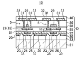
- FIG. 1 is a cross-sectional view showing a main part of a semiconductor device 10 according to the first embodiment.
- FIG. 10 is a plan view schematically showing a main part of an LCD device 1 .
- the LCD device 1 includes a TFT substrate 11 , a counter substrate 12 placed so as to face the TFT substrate 11 , and a liquid crystal layer (not shown) interposed between the TFT substrate 11 and the counter substrate 12 .
- the LCD device 1 has a display area 17 in a region where the TFT substrate 11 overlaps the counter substrate 12 .
- a plurality of pixels 19 are arranged in a matrix pattern in the display area 17 .
- the TFT substrate 11 is comprised of a glass substrate 21 as a transparent support substrate, and has a circuit area 18 in a region that does not overlap the counter substrate 12 .
- a circuit such as a driver for driving and controlling the pixels 19 is directly formed on the glass substrate 21 forming the TFT substrate 11 .
- the drive in this circuit area 18 has TFTs 5 described below.
- a TFT serving as a switching element and a pixel electrode connected thereto are provided for each pixel 19 in the TFT substrate 11 .
- Gate lines and source lines are connected to the TFTs.
- the gate lines and the source lines are extended to the circuit area 18 so as to be connected to the driver etc. at their ends.
- the counter substrate 12 is comprised of a glass substrate as a transparent support substrate, and a color filter, a common electrode, etc. are formed on the surface of the counter substrate 12 , which is located on the side of the TFT substrate 11 .
- a backlight (not shown) as a light source is provided on the opposite side of the TFT substrate 11 from the counter substrate 12 .
- the semiconductor device in the present embodiment is applied as various functional circuits such as the driver directly formed on the glass substrate 21 forming the TFT substrate 11 .
- the semiconductor device 10 includes the glass substrate 21 as a support substrate, and a high-density element portion D formed with high accuracy on the glass substrate 21 .
- a transparent substrate such as the glass substrate 21 is preferable as the support substrate 21 .
- other substrates such as a monocrystalline silicon semiconductor substrate can be used as the support substrate.
- the element portion D has a third insulating film 33 bonded to a flat surface of the glass substrate 21 by self-bonding, the TFTs 5 as semiconductor elements formed over the third insulating film 33 , and light-shielding films 24 provided between the glass substrate 21 and the TFTs 5 .
- the TFTs 5 are, e.g., P-channel metal oxide semiconductor (PMOS) transistors.
- the light-shielding films 24 or back gate electrodes may be formed between the glass substrate 21 and the TFTs 5 .
- An example in which the light-shielding films 24 are formed is described in the present embodiment.
- two TFTs 5 are shown in FIG. 1 , the type of devices that are formed is not limited to the TFTs.
- NMOS N-channel metal oxide semiconductor
- other elements such as bipolar transistors, capacitor elements described later, or diodes can be similarly used as the devices.
- the number of devices is not particularly limited.
- the structure of the semiconductor device 10 will be described in detail below with reference to FIG. 1 .
- a plurality of first recesses 23 and a plurality of second recesses 26 are alternately formed in the opposite surface of the third insulating film 33 from the glass substrate 21 .
- a dummy pattern 20 which is comprised of, e.g., a silicon oxide film etc., is provided in each of the first recesses 23 .
- a second insulating film 22 is formed over the surface of the third insulating film 33 so as to cover the dummy patterns 20 . That is, a part of the second insulating film 22 is provided in the second recesses 26 .
- the second insulating film 22 has a substantially constant thickness. Since the second insulating film 22 is formed along the second recesses 26 , third recesses 38 are formed in those regions of the second insulating film 22 which overlap the second recesses 26 , respectively.
- the second insulating film 22 is comprised of a protective insulating film that suppresses passage of metal ions therethrough. That is, the second insulating film 22 is comprised of, e.g., a dense insulating film such as a silicon nitride film.
- the total thickness of the dummy pattern 20 and the second insulating film 22 overlapping the dummy pattern 20 is equal to that of the light-shielding film 24 and the second insulating film 22 overlapping the light-shielding film 24 .
- the thickness of the third insulating film 33 from the flat surface of the glass substrate 21 is the same both in the regions below the first recesses 23 having the dummy pattern 20 therein, and in the regions below the second recesses 26 having the second insulating film 22 therein.
- the light-shielding films 24 are provided in the third recesses 38 .
- the surfaces of the light-shielding films 24 are flush with the surface of the second insulating film 22 .
- the light-shielding films 24 are comprised of, e.g., a refractory metal such as molybdenum (Mo), titanium nitride (TiN), or tungsten (W).
- the light-shielding films 24 may be configured to function also as back gate electrodes. In this case, characteristics of the TFTs 5 can be dynamically changed by adjusting the potential of the back gate electrodes.
- a first insulating film 25 is formed over the surface of the second insulating film 22 so as to cover the light-shielding films 24 .
- Fourth recesses 39 are formed in the opposite surface of the first insulating film 25 from the second insulating film 22 in those regions which overlap at least a part of the light-shielding film 24 .
- Semiconductor layers 27 are formed in the fourth recesses 39 , and the surfaces of the semiconductor layers 27 are flush with the opposite surface of the first insulating film 25 from the second insulating film 22 . Thus, the semiconductor layers 27 are formed in an island shape in the surface of the first insulating film 25 . At least a part of each semiconductor layer 27 overlaps a corresponding one of the light-shielding films 24 . It is preferable that at least a channel region 51 in each semiconductor layer 27 overlap a corresponding one of the light-shielding films 24 .
- Each semiconductor layer 27 includes the channel region 51 and heavily doped impurity regions 52 formed on both sides (the left and right sides in the figure) of the channel region 51 .
- the semiconductor layers 27 are also referred to as the “base layer.”
- the base layer 15 is comprised of, e.g., a monocrystalline silicon semiconductor layer etc.
- the base layer 1 may be configured to include at least one selected from the group consisting of Group IV semiconductors, Group II-VI compound semiconductors, Group III-V compound semiconductors, Group IV-IV compound semiconductors, alloys containing homologous elements thereof, and oxide semiconductors, instead of the monocrystalline silicon semiconductor layer.
- a part of the base layer 15 is separated and removed along a delamination layer 42 , which is formed by ion implantation of a delamination material such as hydrogen.
- the thickness of the base layer 15 is reduced by separating and removing the part of the base layer 15 in this manner by a heat treatment.
- Gate electrodes 29 are formed on the surface of the gate insulating film 28 so as to overlap the channel regions 51 of the semiconductor layers 27 .
- An interlayer insulating film 30 is formed on the gate insulating film 28 so as to cover the gate electrodes 29 .
- Contact holes 31 are formed so as to extend through the interlayer insulating film 30 at positions on the heavily doped impurity regions 52 of the semiconductor layers 27 .
- interconnect portions (that is, source lines and drain lines) 32 are formed on the surface of the interlayer insulating film 30 and inside the contact holes 31 .
- a protective film 40 is formed over the surface of the interlayer insulating film 30 so as to cover the interconnect portions 32 .
- a method for manufacturing the semiconductor device 10 will be described below with reference to FIGS. 1-9 .
- FIG. 2 is a cross-sectional view showing a base layer 15 having protruding regions 16 .
- FIG. 3 is a cross-sectional view showing a state in which hydrogen ions are implanted into the base layer 15 having a first insulating film 25 .
- FIG. 4 is a cross-sectional view showing the base layer 15 having a delamination layer 42 and light-shielding films 24 .
- FIG. 5 is a cross-sectional view showing the base layer 15 having a second insulating film 22 covering the light-shielding films 24 .
- FIG. 6 is a cross-sectional view showing a silicon oxide film 45 formed on the second insulating film 22 .
- FIG. 7 is a cross-sectional view showing an insulating material layer 46 covering dummy patterns 20 .
- FIG. 8 is a cross-sectional view showing the base layer 15 having a third insulating film 33 .
- FIG. 9 is a cross-sectional view showing the base layer 15 bonded to a glass substrate 21 .
- the surface of a silicon wafer 15 as a base layer 15 is etched to form protruding regions 16 that will serve as semiconductor layers 27 .
- the base layer 15 is a monocrystalline silicon layer.
- a first insulating film 25 having a flat surface is formed on the surface of the base layer 15 . That is, an insulating film is formed so as to cover the protruding regions 16 , and then the surface of the insulting film is planarized by a CMP method etc.
- a delamination material 41 is ion implanted into the base layer 15 having the first insulating film 25 thereon, thereby forming a delaminating layer 42 .
- hydrogen is used as the delamination material 41 .
- An inert element such as helium (He) or neon (Ne) may be used instead of hydrogen. Alternatively, both hydrogen and the inert element may be used.
- the delamination layer 42 can be formed at substantially a constant depth inside the base layer 15 .
- a plurality of light-shielding films 24 are formed on the surface of the first insulating film 25 .
- a refractory metal layer such as Mo, TiN, or W is formed on the surface of the first insulating film 25 , and then the refractory metal layer is etched by photolithography to form the light-shielding films 24 .
- the light-shielding films 24 are formed so that each light-shielding film 24 overlaps at least a part of a corresponding one of the protruding regions 16 .
- back gate electrodes are formed instead of the light-shielding films 24 , the back gate electrodes are formed in a similar manner in this step.
- a second insulating film 22 having an uneven surface reflecting the stepped shape of the light-shielding films 24 is formed over the surface of the first insulating film 25 so as to cover the light-shielding films 24 .
- the second insulating film 22 is, e.g., a dense protective insulating film such as a silicon nitride film. The second insulating film 22 suppresses passage of metal ions therethrough.
- a dummy pattern 20 is formed on the surface of the second insulating film 22 between adjoining ones of the light-shielding films 24 .
- a silicon oxide film 45 as an insulating film is first formed on the entire surface of the second insulating film 22 .
- the thickness of the silicon oxide film 45 is about the same as that of the light-shielding films 45 .
- the silicon oxide film 45 formed on the surface of the second insulating film 22 is etched by using the second insulating film 22 as an etch stopper, thereby forming the dummy patterns 20 as shown in FIG. 7 .
- the height of the dummy patterns 20 is the same as the surface height of the second insulating film 22 on the light-shielding films 24 , based on the surface of the first insulating film 25 , which is located on the side of the second insulating film 22 .
- a third insulating film 33 having a flat surface is formed over the surface of the second insulating film 22 so as to cover the dummy patterns 20 .
- an insulating material layer 46 is first formed over the surface of the second insulating film 22 .
- the interval between the light-shielding film 24 and the dummy pattern 20 (the interval in the direction parallel to the surface of the glass substrate 21 ) is larger than the thickness of the second insulating film 22 , and is smaller than the thickness of the insulating material layer 46 over the light-shielding film 24 . This reduces the possibility of formation of large recesses in the surface of the insulating material layer 46 in each region between the dummy pattern 20 and the light-shielding film 24 .
- the surface of the insulating material layer 46 is polished and planarized by a CMP method etc. to form the third insulating film 33 .
- the base layer 15 provided with the third insulating film 33 and having a part of the element portion D formed thereon is bonded to the glass substrate 21 as a support substrate so that the flat surface of the third insulating film 33 faces the glass substrate 21 .
- the surface of the third insulating film 33 is bonded to the surface of the glass substrate 21 by self-bonding due to the van der Waals force.
- the base layer 15 bonded to the glass substrate 21 is separated and removed along the delamination layer 42 .
- the base layer 15 bonded to the glass substrate 21 is heated to about 400-600° C. to separate and remove along the delamination layer 42 a part of the base layer 15 , which is located on the opposite side of the delamination layer 42 from the glass substrate 21 .
- the base layer 15 remaining over the glass substrate 21 is etched by using the first insulating film 25 around each protruding region 16 as an etch stopper, thereby forming semiconductor layers 27 forming TFTs as semiconductor elements.
- the semiconductor layers 27 are formed so that at least a part of each semiconductor layer 27 overlaps a corresponding one of the light-shielding films 24 .
- the protruding regions 16 of the base layer 15 are left in an island shape as the semiconductor layers 27 .
- a gate insulating film 28 is formed so as to cover the semiconductor layers 27 .
- the gate insulating film 28 is formed to have a flat surface along the surfaces of the semiconductor layers 27 and the first insulating film 25 .
- gate electrodes 29 are formed on the surface of the gate insulating film 28 so as to overlap channel regions 51 of the semiconductor layers 27 .
- each semiconductor layer 27 is doped with an impurity element to form a heavily doped impurity region 52 .
- the semiconductor layers 27 are doped with the impurity element by using the gate electrodes 29 as a mask.
- the heavily doped impurity region 52 is formed in a region of each semiconductor layer 27 , which does not overlap a corresponding one of the gate electrodes 29
- the channel region 51 is formed in a region of each semiconductor layer 27 , which overlaps a corresponding one of the gate electrodes 29 .
- contact holes 31 are formed in the interlayer insulating film 30 etc.
- a metal layer formed on the interlayer insulating film 30 is patterned by photolithography to form a plurality of interconnect portions 32 .
- the semiconductor device 1 is manufactured by the steps described above.
- the dummy patterns 20 are formed on the surface of the second insulating film 22 so that the height of the dummy patterns 20 is equal to that of the second insulating film 22 on the light-shielding films 24 , as measured from the surface of the first insulating film 25 .
- This allows the total thickness of the dummy pattern 20 and the second insulating film 22 overlapping the dummy pattern 20 to be equal to that of the light-shielding film 24 and the second insulating film 22 overlapping the light-shielding film 24 , on the flat surface of the first insulating film 25 .
- the third insulating film 33 covering the light-shielding films 24 can be planarized with high accuracy on the base layer 15 by a CMP method regardless of the shape of the light-shielding films 24 . This makes it easier to perform the subsequent step of bonding the base layer 15 to the glass substrate 21 , and also eliminates the need to perform the CMP treatment on the large-size glass substrate 21 .
- the interval between the light-shielding film 24 and the dummy pattern 20 is larger than the thickness of the second insulating film 22 , and is smaller than the thickness of the insulating material layer 46 over the light-shielding film 24 .
- the surface of the insulating material layer 46 can be easily planarized with high accuracy.
- the dummy patterns 20 are formed after forming the second insulating film 22 comprised of a dense protective insulating film such as a silicon nitride film. Accordingly, even if the glass substrate 21 is used as the support substrate, the second insulating film 22 suppresses passage of metal ions (mobile ions) therethrough from the side of the glass substrate 21 , and the possibility of variation in characteristics of the TFTs 5 as semiconductor elements can be reduced. Moreover, since the second insulating film 22 can be used as an etch stopper, the dummy patterns 20 can be more easily formed with higher accuracy while reducing the possibility of corrosion of a lower layer such as the light-shielding films 24 .
- the dummy patterns 20 are comprised of a silicon oxide film, the possibility of an unnecessary increase in load capacitance can be reduced and reduction in aperture ratio of the LCD device 1 can be suppressed, as compared to the case where the dummy patterns 20 are comprised of a metal film.
- the delamination material 41 can be ion implanted into the base layer 15 before forming the light-shielding films 24 , ions can be implanted to a uniform depth in the base layer 15 , which allows the delamination layer 42 to be formed at a uniform depth position in the base layer 15 .
- the light-shielding films 24 are formed in advance in the base layer 15 before bonding the base layer 15 to the glass substrate 21 . This eliminates the need to align the light-shielding films with the semiconductor layers with high accuracy in the step of bonding the base layer to the glass substrate as in conventional examples, and also allows the desired regions of the semiconductor layers 27 to be more easily covered by the light-shielding films 24 .
- Forming new interconnect layers from the light-shielding films 24 can reduce the size of the circuit configuration that is formed in the glass substrate 21 .
- bonding the base layer 15 to the glass substrate 21 can facilitate formation of flat semiconductor layers 27 . Since the semiconductor layers 27 do not have a stepped shape, the thickness of the gate insulating film 28 can be easily reduced. This allows the threshold voltage in the semiconductor layers 27 to be controlled with high accuracy, and thus can reduce power consumption of the semiconductor device 10 .
- the semiconductor layers 27 are comprised of monocrystalline silicon, the possibility of a leakage current due to crystal defects can be reduced. This can significantly improve characteristics of the TFTs 5 having the semiconductor layers 27 .
- FIGS. 11-19 show a second embodiment of the present invention.
- FIG. 11 is a cross-sectional view showing a main part of a semiconductor device 10 according to the second embodiment. Note that in the following embodiments, the same portions as those in FIGS. 1-10 are denoted with the same reference characters, and detailed description thereof will be omitted.
- the semiconductor layers 27 are formed in the fourth recesses 39 in the first insulating film 25 . In the second embodiment, however, semiconductor layers 27 are formed on a flat surface of a first insulating film 25 .
- the total thickness of the dummy pattern 20 and the second insulating film 22 overlapping the dummy pattern 20 is equal to that of the light-shielding film 24 and the second insulating film 22 overlapping the light-shielding film 24 .
- the first insulating film 25 provided on the surfaces of the light-shielding films 24 and the surface of the second insulating film 22 has a flat surface.
- the semiconductor layers 27 are formed in an island shape on the flat surface of the first insulating film 25 .
- the gate insulating film 28 covers the semiconductor layers 27 , and has a convex surface in those regions where the gate insulating film 28 covers the semiconductor layers 27 .
- a method for manufacturing the semiconductor device 10 will be described below with reference to FIGS. 12-19 .
- FIG. 12 is a cross-sectional view showing a base layer 15 having a delamination layer 42 .
- FIG. 13 is a cross-sectional view showing the base layer 15 having light-shielding films 24 .
- FIG. 14 is a cross-sectional view showing the base layer 15 having a second insulating film 22 covering the light-shielding films 24 .
- FIG. 15 is a cross-sectional view showing a silicon oxide film 45 formed on the second insulating film 22 .
- FIG. 16 is a cross-sectional view showing an insulating material layer 46 covering dummy patterns 20 .
- FIG. 17 is a cross-sectional view showing the base layer 15 having a third insulating film 33 .
- FIG. 18 is a cross-sectional view showing the base layer 15 bonded to a glass substrate 21 .
- FIG. 19 is a cross-sectional view showing the base layer 15 having semiconductor layers 27 .
- a first insulating film 25 is formed on the surface of a silicon wafer 15 as a base layer 15 . Since the base layer 15 has a flat surface, the first insulating film 25 is also formed with a flat surface.
- a delamination material 41 is ion implanted into the base layer 15 having the first insulating film 25 thereon, thereby forming a delaminating layer 42 .
- hydrogen or an inert element He, Ne, etc.
- the delamination layer 42 can be formed at a substantially constant depth inside the base layer 15 .
- light-shielding films 24 are formed on the surface of the first insulating film 25 .
- a refractory metal layer such as Mo, TiN, or W is formed on the surface of the first insulating film 25 , and then the refractory metal layer is etched by photolithography to form the light-shielding films 24 .
- a second insulating film 22 having an uneven surface reflecting the stepped shape of the light-shielding films 24 is formed over the surface of the first insulating film 25 so as to cover the light-shielding films 24 .
- the second insulating film 22 is, e.g., a dense protective insulating film such as a silicon nitride film.
- a dummy pattern 20 is formed on the surface of the second insulating film 22 between adjoining ones of the light-shielding films 24 .
- a silicon oxide film 45 as an insulating film is first formed on the entire surface of the second insulating film 22 .
- the thickness of the silicon oxide film 45 is about the same as that of the light-shielding films 45 .
- the silicon oxide film 45 formed on the surface of the second insulating film 22 is etched by using the second insulating film 22 as an etch stopper, thereby forming the dummy patterns 20 as shown in FIG. 16 .
- an insulating material layer 46 is first formed over the surface of the second insulating film 22 . Then, as shown in FIG. 17 , the surface of the insulating material layer 46 is polished and planarized by a CMP method etc. to form a third insulating film 33 .
- the base layer 15 provided with the light-shielding films 24 is bonded to a glass substrate 21 so that the flat surface of the third insulating film 33 faces the glass substrate 21 .
- the surface of the third insulating film 33 is bonded to the surface of the glass substrate 21 by self-bonding due to the van der Waals force.
- the base layer 15 remaining over the glass substrate 21 is etched to form protruding regions 56 as semiconductor layers 27 .
- the protruding regions 56 are formed so that each protruding region 56 overlaps at least a part of a corresponding one of the light-shielding films 24 .
- the protruding regions 56 are formed in an island shape as shown in FIG. 19 .
- a gate insulating film 28 is formed so as to cover the semiconductor layers 27 .
- the gate insulating film 28 is formed to have a convex surface along the surfaces of the semiconductor layers 27 .
- gate electrodes 29 are formed on the surface of the gate insulating film 28 so as to overlap channel regions 51 of the semiconductor layers 27 .
- the semiconductor layers 27 are doped with an impurity element by using the gate electrodes 29 as a mask.
- a heavily doped impurity region 52 is formed in a region of each semiconductor layer 27 , which does not overlap a corresponding one of the gate electrodes 29
- the channel region 51 is formed in a region of each semiconductor layer 27 , which overlaps a corresponding one of the gate electrodes 29 .
- contact holes 31 are formed in an interlayer insulating film 30 etc., and a plurality of interconnect portions 32 are formed.
- the semiconductor device 1 is manufactured by the steps described above.
- the third insulating film 33 covering the light-shielding films 24 can be planarized with high accuracy over the base layer 15 by a CMP method regardless of the shape of the light-shielding films 24 .
- the protruding regions 56 are not formed in advance in the base layer 15 before forming the first insulating film 25 , hydrogen can be ion implanted into the base layer 15 via the base layer 15 and the first insulating film 25 both having a flat surface. This allows the delamination layer 42 to be formed at a more uniform depth position in the base layer 15 .
- the total number of times the planarizing step is performed by using a CMP method can be reduced to one, which is performed when forming the third insulating film 33 .
- FIG. 20 shows a third embodiment of the present invention.
- FIG. 20 is a cross-sectional view showing a main part of a semiconductor device 10 according to the third embodiment.
- FIG. 21 is a graph showing the voltage-capacitance relation in a first capacitor element 6 a and a second capacitor element 6 b.
- the semiconductor elements included in the semiconductor devices 10 of the first and second embodiments are the TFTs 5
- at least one of semiconductor elements included in the semiconductor device 10 of the third embodiment is a capacitor element 6 a , 6 b.
- the semiconductor device 10 of the present embodiment includes a glass substrate 21 as a support substrate, and a high-density element portion D formed with high accuracy on the glass substrate 21 .
- the element portion D includes a first capacitor element 6 a and a second capacitor element 6 b.
- the first capacitor element 6 a has a back gate electrode 54 as one capacitor electrode, and a semiconductor layer 27 (a heavily doped impurity region 52 ) doped with an N+ type impurity element and placed as the other capacitor electrode so as to face the back gate electrode 54 .
- the second capacitor element 6 b has a semiconductor layer 27 (a channel region 51 and a heavily doped impurity region 52 ) as one capacitor electrode, and an electrode layer 55 placed as the other capacitor electrode so as to face the semiconductor layer 27 .
- a plurality of first recesses 23 and a plurality of second recesses 26 are alternately formed in a flat substrate of the glass substrate 21 .
- a dummy pattern 20 which is comprised of, e.g., a silicon oxide film etc., is provided in each of the first recesses 23 .
- a second insulating film 22 is formed over the surface of a third insulating film 33 so as to cover the dummy patterns 20 . That is, a part of the second insulating film 22 is provided in the second recesses 26 .
- the second insulating film 22 has a substantially constant thickness. Since the second insulating film 22 is formed along the second recesses 26 , third recesses 38 are formed in those regions of the second insulating film 22 which overlap the second recesses 26 , respectively.
- the second insulating film 22 is comprised of, e.g., a dense insulating film such as a silicon nitride film.
- the total thickness of the dummy pattern 20 and the second insulating film 22 overlapping the dummy pattern 20 is equal to that of a light-shielding film 24 and the second insulating film 22 overlapping the light-shielding film 24 , as in the first and second embodiments.
- the back gate electrode 54 or the light-shielding film 24 is provided in each of the third recesses 38 .
- the respective surfaces of the back gate electrode 54 and the light-shielding film 24 are flush with the surface of the second insulating film 22 .
- the back gate electrode 54 and the light-shielding film 24 are comprised of, e.g., a refractory metal such as Mo, TiN, or W.
- a first insulating film 25 is formed over the surface of the second insulating film 22 so as to cover the back gate electrode 54 and the light-shielding film 24 .
- Fourth recesses 39 are formed in the opposite surface of the first insulating film 25 from the second insulating film 22 in those regions which overlap either at least a part of the back gate electrode 54 or at least a part of the light-shielding film 24 .
- At least a part of each semiconductor layer 27 overlaps the back gate electrode 54 or the light-shielding film 24 .
- the semiconductor layers 27 are formed in the fourth recesses 39 , and the surfaces of the semiconductor layers 27 are flush with the opposite surface of the first insulating film 25 from the second insulating film 22 . Thus, the semiconductor layers 27 are formed in an island shape in the surface of the first insulating film 25 .
- the heavily doped impurity region 52 forming the first capacitor element 6 a is provided in the fourth recess 39 facing the back gate electrode 54 .
- the channel region 51 and the heavily doped impurity region 52 , which form the second capacitor element 6 b are provided in the fourth recess 39 facing the light-shielding film 24 .
- a part of the base layer 15 has been separated and removed along a delamination layer 42 formed by ion implantation of a delamination material such as hydrogen.
- the base layer 15 has been reduced in thickness by separating and removing the part of the base layer 15 by a heat treatment.
- the surfaces of the semiconductor layers 27 and the surface of the first insulating film 25 are directly covered by a gate insulating film 28 .
- the electrode layer 55 is formed on the surface of the gate insulating film 28 so as to overlap the channel region 51 of the semiconductor layer 27 that forms the second capacitor element 6 b.
- An interlayer insulating film 30 is formed over the gate insulating film 28 so as to cover the electrode layer 55 .
- Contact holes 31 are formed so as to extend through the interlayer insulating film 30 at positions on the electrode layer 55 , the back gate electrode 54 , and the heavily doped impurity regions 52 .
- interconnect portions 32 are formed on the surface of the interlayer insulating film 30 and inside the contact holes 31 .
- a protective film 40 is formed over the surface of the interlayer insulating film 30 so as to cover the interconnect portions 32 .
- the semiconductor device 10 of the present embodiment can be manufactured in a manner similar to that of the first embodiment. At least one of the semiconductor elements, a semiconductor layer (a heavily doped impurity region 52 ) doped with an impurity element and a back gate element 54 are formed so as to face each other, thereby forming a capacitor element 6 a having the heavily doped impurity region 52 and the back gate electrode 54 as a pair of capacitor electrodes.
- the protruding region formation step, the first insulating film formation step, and the delamination layer formation step are sequentially performed as in the first embodiment. Then, in the light-shielding film formation step, the light-shielding film 24 and the back gate electrode 54 are formed at the same time. Like the light-shielding film 24 , the back gate electrode 54 is also formed by patterning a refractory metal layer by photolithography and etching.
- the second insulating film formation step the dummy pattern formation step, the third insulating film formation step, the bonding step, the separating step, the semiconductor layer formation step, and the gate insulating film formation step are sequentially performed.
- semiconductor layers 27 are formed which serve as capacitor electrodes of a first capacitor element 6 and a second capacitor element 6 b.
- an electrode layer 55 is formed so as to overlap the channel region 51 , as in the gate electrode formation step.
- the heavily doped impurity region formation step is performed, in which at least a part of each semiconductor layer 27 is doped with an impurity element to form heavily doped impurity regions 52 .
- contact holes 31 are formed in the interlayer insulating film 30 etc.
- a metal layer formed on the interlayer insulating film 30 is patterned by photolithography to form a plurality of interconnect portions 32 .
- the semiconductor device 10 is manufactured by the steps described above.
- the third insulating film 33 covering both the back gate electrode 54 and the light-shielding film 24 can be planarized with high accuracy over the base layer 15 by a CMP method regardless of the shapes of the back gate electrode 54 and the light-shielding film 24 .
- the light-shielding film 24 overlapping the channel region 51 of the semiconductor layer 27 is provided for the second capacitor element 6 b , light incidence on the channel region 51 can be blocked, and the possibility of malfunctions can be reduced.
- one of the capacitor electrodes is comprised of the channel region 51 of the semiconductor layer 27 .
- capacitance C is produced by an applied voltage higher than the threshold voltage.
- one of the capacitor electrodes is comprised of the heavily doped impurity region 52 as the entire semiconductor layer 27 .
- capacitance C is constant regardless of the applied voltage. That is, the first capacitor element 6 a can be used as a capacitor element that is stable in a wide applied-voltage range.
- the semiconductor device 10 is used as various functional circuits such as a driver formed directly on the glass substrate 21 .
- the present invention is not limited to this.
- the semiconductor device 10 can be similarly used as a semiconductor device having TFTs that are formed at each pixel to drive pixel electrodes.
- the present invention is similarly applicable to semiconductor devices for use in, e.g., display devices other than LCD devices, such as organic electroluminescent (EL) display devices.
- display devices other than LCD devices, such as organic electroluminescent (EL) display devices.
- EL organic electroluminescent
- the present invention is useful for semiconductor devices for use in, e.g., LCD devices, and manufacturing methods thereof.
Landscapes
- Physics & Mathematics (AREA)
- Nonlinear Science (AREA)
- Engineering & Computer Science (AREA)
- Microelectronics & Electronic Packaging (AREA)
- Mathematical Physics (AREA)
- Chemical & Material Sciences (AREA)
- Crystallography & Structural Chemistry (AREA)
- General Physics & Mathematics (AREA)
- Optics & Photonics (AREA)
- Power Engineering (AREA)
- Thin Film Transistor (AREA)
- Liquid Crystal (AREA)
Applications Claiming Priority (3)
| Application Number | Priority Date | Filing Date | Title |
|---|---|---|---|
| JP2009230768 | 2009-10-02 | ||
| JP2009-230768 | 2009-10-02 | ||
| PCT/JP2010/003814 WO2011039907A1 (ja) | 2009-10-02 | 2010-06-08 | 半導体装置及びその製造方法 |
Publications (2)
| Publication Number | Publication Date |
|---|---|
| US20120119322A1 US20120119322A1 (en) | 2012-05-17 |
| US8569147B2 true US8569147B2 (en) | 2013-10-29 |
Family
ID=43825761
Family Applications (1)
| Application Number | Title | Priority Date | Filing Date |
|---|---|---|---|
| US13/386,085 Expired - Fee Related US8569147B2 (en) | 2009-10-02 | 2010-06-08 | Semiconductor device and manufacturing method thereof |
Country Status (3)
| Country | Link |
|---|---|
| US (1) | US8569147B2 (ja) |
| CN (1) | CN102473643B (ja) |
| WO (1) | WO2011039907A1 (ja) |
Cited By (2)
| Publication number | Priority date | Publication date | Assignee | Title |
|---|---|---|---|---|
| US20220190079A1 (en) * | 2020-12-11 | 2022-06-16 | Lg Display Co., Ltd. | Organic Light Emitting Display Device |
| US12238971B2 (en) * | 2020-12-18 | 2025-02-25 | Samsung Display Co., Ltd. | Display apparatus |
Families Citing this family (7)
| Publication number | Priority date | Publication date | Assignee | Title |
|---|---|---|---|---|
| US9818765B2 (en) | 2013-08-26 | 2017-11-14 | Apple Inc. | Displays with silicon and semiconducting oxide thin-film transistors |
| US10684500B2 (en) * | 2015-05-27 | 2020-06-16 | Semiconductor Energy Laboratory Co., Ltd. | Touch panel |
| KR102521897B1 (ko) * | 2017-12-26 | 2023-04-18 | 삼성디스플레이 주식회사 | 표시 패널, 표시 장치 및 표시 패널 제조 방법 |
| JP2020144252A (ja) * | 2019-03-07 | 2020-09-10 | セイコーエプソン株式会社 | 電気光学装置、電子機器、および電気光学装置の製造方法 |
| KR102760409B1 (ko) * | 2019-04-12 | 2025-02-04 | 삼성디스플레이 주식회사 | 표시 장치 |
| KR102651064B1 (ko) * | 2019-07-30 | 2024-03-25 | 삼성디스플레이 주식회사 | 표시 장치 |
| US12469639B2 (en) * | 2021-03-09 | 2025-11-11 | Tdk Corporation | Method for manufacturing multilayer coil component |
Citations (11)
| Publication number | Priority date | Publication date | Assignee | Title |
|---|---|---|---|---|
| JPH02177435A (ja) | 1988-12-28 | 1990-07-10 | Sony Corp | 半導体基板の製法 |
| JPH04307972A (ja) | 1991-04-05 | 1992-10-30 | Fujitsu Ltd | 半導体装置の製造方法 |
| JPH10293320A (ja) | 1997-04-22 | 1998-11-04 | Seiko Epson Corp | Soi基板とその製造方法及びこれを用いた半導体装置及び液晶パネル |
| US5882987A (en) * | 1997-08-26 | 1999-03-16 | International Business Machines Corporation | Smart-cut process for the production of thin semiconductor material films |
| JPH1197654A (ja) | 1997-09-17 | 1999-04-09 | Denso Corp | 半導体基板の製造方法 |
| JPH11112000A (ja) | 1997-10-06 | 1999-04-23 | Denso Corp | 半導体装置 |
| JP2000236095A (ja) | 1999-02-17 | 2000-08-29 | Fujitsu Ltd | 半導体装置の製造方法 |
| JP2000340795A (ja) | 1999-05-26 | 2000-12-08 | Sony Corp | 半導体論理素子およびそれを用いた論理回路 |
| JP2001028354A (ja) | 1999-05-12 | 2001-01-30 | Sony Corp | 半導体装置の製造方法 |
| US6191007B1 (en) | 1997-04-28 | 2001-02-20 | Denso Corporation | Method for manufacturing a semiconductor substrate |
| US6531403B2 (en) * | 2000-03-30 | 2003-03-11 | Kabushiki Kaisha Toshiba | Method of etching an object, method of repairing pattern, nitride pattern and semiconductor device |
Family Cites Families (1)
| Publication number | Priority date | Publication date | Assignee | Title |
|---|---|---|---|---|
| JP2003167534A (ja) * | 2001-09-21 | 2003-06-13 | Seiko Epson Corp | 電気光学装置及びその製造方法並びに電子機器 |
-
2010
- 2010-06-08 WO PCT/JP2010/003814 patent/WO2011039907A1/ja not_active Ceased
- 2010-06-08 CN CN201080029882.4A patent/CN102473643B/zh not_active Expired - Fee Related
- 2010-06-08 US US13/386,085 patent/US8569147B2/en not_active Expired - Fee Related
Patent Citations (11)
| Publication number | Priority date | Publication date | Assignee | Title |
|---|---|---|---|---|
| JPH02177435A (ja) | 1988-12-28 | 1990-07-10 | Sony Corp | 半導体基板の製法 |
| JPH04307972A (ja) | 1991-04-05 | 1992-10-30 | Fujitsu Ltd | 半導体装置の製造方法 |
| JPH10293320A (ja) | 1997-04-22 | 1998-11-04 | Seiko Epson Corp | Soi基板とその製造方法及びこれを用いた半導体装置及び液晶パネル |
| US6191007B1 (en) | 1997-04-28 | 2001-02-20 | Denso Corporation | Method for manufacturing a semiconductor substrate |
| US5882987A (en) * | 1997-08-26 | 1999-03-16 | International Business Machines Corporation | Smart-cut process for the production of thin semiconductor material films |
| JPH1197654A (ja) | 1997-09-17 | 1999-04-09 | Denso Corp | 半導体基板の製造方法 |
| JPH11112000A (ja) | 1997-10-06 | 1999-04-23 | Denso Corp | 半導体装置 |
| JP2000236095A (ja) | 1999-02-17 | 2000-08-29 | Fujitsu Ltd | 半導体装置の製造方法 |
| JP2001028354A (ja) | 1999-05-12 | 2001-01-30 | Sony Corp | 半導体装置の製造方法 |
| JP2000340795A (ja) | 1999-05-26 | 2000-12-08 | Sony Corp | 半導体論理素子およびそれを用いた論理回路 |
| US6531403B2 (en) * | 2000-03-30 | 2003-03-11 | Kabushiki Kaisha Toshiba | Method of etching an object, method of repairing pattern, nitride pattern and semiconductor device |
Non-Patent Citations (1)
| Title |
|---|
| Official Communication issued in International Patent Application No. PCT/JP2010/003814, mailed on Sep. 7, 2010. |
Cited By (4)
| Publication number | Priority date | Publication date | Assignee | Title |
|---|---|---|---|---|
| US20220190079A1 (en) * | 2020-12-11 | 2022-06-16 | Lg Display Co., Ltd. | Organic Light Emitting Display Device |
| US11871616B2 (en) * | 2020-12-11 | 2024-01-09 | Lg Display Co., Ltd. | Organic light emitting display device |
| US12250850B2 (en) | 2020-12-11 | 2025-03-11 | Lg Display Co., Ltd. | Organic light emitting display device comprising multi type thin film transistor |
| US12238971B2 (en) * | 2020-12-18 | 2025-02-25 | Samsung Display Co., Ltd. | Display apparatus |
Also Published As
| Publication number | Publication date |
|---|---|
| WO2011039907A1 (ja) | 2011-04-07 |
| CN102473643A (zh) | 2012-05-23 |
| US20120119322A1 (en) | 2012-05-17 |
| CN102473643B (zh) | 2015-04-01 |
Similar Documents
| Publication | Publication Date | Title |
|---|---|---|
| US8569147B2 (en) | Semiconductor device and manufacturing method thereof | |
| JP7703600B2 (ja) | 液晶表示装置 | |
| JP5162050B2 (ja) | 半導体素子、半導体素子の製造方法、アクティブマトリクス基板及び表示装置 | |
| JP5150555B2 (ja) | キャパシタ及び薄膜トランジスタを有する基板、これを具備した平板ディスプレイ装置及び該キャパシタ及び薄膜トランジスタを有する基板の製造方法 | |
| TWI401802B (zh) | 薄膜電晶體板及其製造方法 | |
| US7973317B2 (en) | Array substrate for liquid crystal display and method for fabricating the same | |
| TW201022814A (en) | Display device | |
| US8420458B2 (en) | Semiconductor device and method of producing same | |
| US20080164483A1 (en) | Semiconductor Device and Manufacturing Method Thereof, and Liquid Crystal Display Device | |
| US6713328B2 (en) | Manufacturing method of thin film transistor panel | |
| JP4366953B2 (ja) | 複合半導体基板の製造方法 | |
| US20100283104A1 (en) | Semiconductor device and method for manufacturing the same | |
| JP2008218626A (ja) | Tftアレイ基板及びその製造方法 | |
| US20110042693A1 (en) | Semiconductor device and manufacturing method thereof | |
| JP4529170B2 (ja) | 薄膜トランジスタ、tft基板、及び、液晶表示装置 | |
| JP4366954B2 (ja) | 複合半導体基板の製造方法 | |
| US8481375B2 (en) | Semiconductor device and method for producing the same | |
| JP2009064831A (ja) | 半導体装置、表示装置及びそれらの製造方法 | |
| JP4442189B2 (ja) | 半導体装置、平面表示装置およびそれらの製造方法 | |
| JP4102788B2 (ja) | 液晶表示装置の製造方法 | |
| US8354329B2 (en) | Semiconductor device manufacturing method, semiconductor device and display apparatus | |
| KR20070040017A (ko) | 박막 트랜지스터 및 이의 제조방법 | |
| JP2006259241A (ja) | 電気光学装置の製造方法 | |
| KR20010009012A (ko) | 액정표시장치의 박막트랜지스터측 판넬 및 그 형성방법 | |
| JP2005223027A (ja) | 表示装置およびその製造方法 |
Legal Events
| Date | Code | Title | Description |
|---|---|---|---|
| AS | Assignment |
Owner name: SHARP KABUSHIKI KAISHA, JAPAN Free format text: ASSIGNMENT OF ASSIGNORS INTEREST;ASSIGNOR:TADA, KENSHI;REEL/FRAME:027566/0165 Effective date: 20111222 |
|
| STCF | Information on status: patent grant |
Free format text: PATENTED CASE |
|
| FEPP | Fee payment procedure |
Free format text: PAYOR NUMBER ASSIGNED (ORIGINAL EVENT CODE: ASPN); ENTITY STATUS OF PATENT OWNER: LARGE ENTITY |
|
| FPAY | Fee payment |
Year of fee payment: 4 |
|
| FEPP | Fee payment procedure |
Free format text: MAINTENANCE FEE REMINDER MAILED (ORIGINAL EVENT CODE: REM.); ENTITY STATUS OF PATENT OWNER: LARGE ENTITY |
|
| LAPS | Lapse for failure to pay maintenance fees |
Free format text: PATENT EXPIRED FOR FAILURE TO PAY MAINTENANCE FEES (ORIGINAL EVENT CODE: EXP.); ENTITY STATUS OF PATENT OWNER: LARGE ENTITY |
|
| STCH | Information on status: patent discontinuation |
Free format text: PATENT EXPIRED DUE TO NONPAYMENT OF MAINTENANCE FEES UNDER 37 CFR 1.362 |
|
| FP | Lapsed due to failure to pay maintenance fee |
Effective date: 20211029 |