WO2011007709A1 - 成膜方法 - Google Patents
成膜方法 Download PDFInfo
- Publication number
- WO2011007709A1 WO2011007709A1 PCT/JP2010/061595 JP2010061595W WO2011007709A1 WO 2011007709 A1 WO2011007709 A1 WO 2011007709A1 JP 2010061595 W JP2010061595 W JP 2010061595W WO 2011007709 A1 WO2011007709 A1 WO 2011007709A1
- Authority
- WO
- WIPO (PCT)
- Prior art keywords
- film
- insulating film
- forming method
- film forming
- manganese
- Prior art date
- Legal status (The legal status is an assumption and is not a legal conclusion. Google has not performed a legal analysis and makes no representation as to the accuracy of the status listed.)
- Ceased
Links
Images












Classifications
-
- H—ELECTRICITY
- H10—SEMICONDUCTOR DEVICES; ELECTRIC SOLID-STATE DEVICES NOT OTHERWISE PROVIDED FOR
- H10W—GENERIC PACKAGES, INTERCONNECTIONS, CONNECTORS OR OTHER CONSTRUCTIONAL DETAILS OF DEVICES COVERED BY CLASS H10
- H10W20/00—Interconnections in chips, wafers or substrates
- H10W20/40—Interconnections external to wafers or substrates, e.g. back-end-of-line [BEOL] metallisations or vias connecting to gate electrodes
- H10W20/41—Interconnections external to wafers or substrates, e.g. back-end-of-line [BEOL] metallisations or vias connecting to gate electrodes characterised by their conductive parts
- H10W20/425—Barrier, adhesion or liner layers
-
- C—CHEMISTRY; METALLURGY
- C23—COATING METALLIC MATERIAL; COATING MATERIAL WITH METALLIC MATERIAL; CHEMICAL SURFACE TREATMENT; DIFFUSION TREATMENT OF METALLIC MATERIAL; COATING BY VACUUM EVAPORATION, BY SPUTTERING, BY ION IMPLANTATION OR BY CHEMICAL VAPOUR DEPOSITION, IN GENERAL; INHIBITING CORROSION OF METALLIC MATERIAL OR INCRUSTATION IN GENERAL
- C23C—COATING METALLIC MATERIAL; COATING MATERIAL WITH METALLIC MATERIAL; SURFACE TREATMENT OF METALLIC MATERIAL BY DIFFUSION INTO THE SURFACE, BY CHEMICAL CONVERSION OR SUBSTITUTION; COATING BY VACUUM EVAPORATION, BY SPUTTERING, BY ION IMPLANTATION OR BY CHEMICAL VAPOUR DEPOSITION, IN GENERAL
- C23C16/00—Chemical coating by decomposition of gaseous compounds, without leaving reaction products of surface material in the coating, i.e. chemical vapour deposition [CVD] processes
- C23C16/02—Pretreatment of the material to be coated
-
- C—CHEMISTRY; METALLURGY
- C23—COATING METALLIC MATERIAL; COATING MATERIAL WITH METALLIC MATERIAL; CHEMICAL SURFACE TREATMENT; DIFFUSION TREATMENT OF METALLIC MATERIAL; COATING BY VACUUM EVAPORATION, BY SPUTTERING, BY ION IMPLANTATION OR BY CHEMICAL VAPOUR DEPOSITION, IN GENERAL; INHIBITING CORROSION OF METALLIC MATERIAL OR INCRUSTATION IN GENERAL
- C23C—COATING METALLIC MATERIAL; COATING MATERIAL WITH METALLIC MATERIAL; SURFACE TREATMENT OF METALLIC MATERIAL BY DIFFUSION INTO THE SURFACE, BY CHEMICAL CONVERSION OR SUBSTITUTION; COATING BY VACUUM EVAPORATION, BY SPUTTERING, BY ION IMPLANTATION OR BY CHEMICAL VAPOUR DEPOSITION, IN GENERAL
- C23C16/00—Chemical coating by decomposition of gaseous compounds, without leaving reaction products of surface material in the coating, i.e. chemical vapour deposition [CVD] processes
- C23C16/02—Pretreatment of the material to be coated
- C23C16/0227—Pretreatment of the material to be coated by cleaning or etching
- C23C16/0236—Pretreatment of the material to be coated by cleaning or etching by etching with a reactive gas
-
- C—CHEMISTRY; METALLURGY
- C23—COATING METALLIC MATERIAL; COATING MATERIAL WITH METALLIC MATERIAL; CHEMICAL SURFACE TREATMENT; DIFFUSION TREATMENT OF METALLIC MATERIAL; COATING BY VACUUM EVAPORATION, BY SPUTTERING, BY ION IMPLANTATION OR BY CHEMICAL VAPOUR DEPOSITION, IN GENERAL; INHIBITING CORROSION OF METALLIC MATERIAL OR INCRUSTATION IN GENERAL
- C23C—COATING METALLIC MATERIAL; COATING MATERIAL WITH METALLIC MATERIAL; SURFACE TREATMENT OF METALLIC MATERIAL BY DIFFUSION INTO THE SURFACE, BY CHEMICAL CONVERSION OR SUBSTITUTION; COATING BY VACUUM EVAPORATION, BY SPUTTERING, BY ION IMPLANTATION OR BY CHEMICAL VAPOUR DEPOSITION, IN GENERAL
- C23C16/00—Chemical coating by decomposition of gaseous compounds, without leaving reaction products of surface material in the coating, i.e. chemical vapour deposition [CVD] processes
- C23C16/04—Coating on selected surface areas, e.g. using masks
-
- C—CHEMISTRY; METALLURGY
- C23—COATING METALLIC MATERIAL; COATING MATERIAL WITH METALLIC MATERIAL; CHEMICAL SURFACE TREATMENT; DIFFUSION TREATMENT OF METALLIC MATERIAL; COATING BY VACUUM EVAPORATION, BY SPUTTERING, BY ION IMPLANTATION OR BY CHEMICAL VAPOUR DEPOSITION, IN GENERAL; INHIBITING CORROSION OF METALLIC MATERIAL OR INCRUSTATION IN GENERAL
- C23C—COATING METALLIC MATERIAL; COATING MATERIAL WITH METALLIC MATERIAL; SURFACE TREATMENT OF METALLIC MATERIAL BY DIFFUSION INTO THE SURFACE, BY CHEMICAL CONVERSION OR SUBSTITUTION; COATING BY VACUUM EVAPORATION, BY SPUTTERING, BY ION IMPLANTATION OR BY CHEMICAL VAPOUR DEPOSITION, IN GENERAL
- C23C16/00—Chemical coating by decomposition of gaseous compounds, without leaving reaction products of surface material in the coating, i.e. chemical vapour deposition [CVD] processes
- C23C16/04—Coating on selected surface areas, e.g. using masks
- C23C16/042—Coating on selected surface areas, e.g. using masks using masks
-
- C—CHEMISTRY; METALLURGY
- C23—COATING METALLIC MATERIAL; COATING MATERIAL WITH METALLIC MATERIAL; CHEMICAL SURFACE TREATMENT; DIFFUSION TREATMENT OF METALLIC MATERIAL; COATING BY VACUUM EVAPORATION, BY SPUTTERING, BY ION IMPLANTATION OR BY CHEMICAL VAPOUR DEPOSITION, IN GENERAL; INHIBITING CORROSION OF METALLIC MATERIAL OR INCRUSTATION IN GENERAL
- C23C—COATING METALLIC MATERIAL; COATING MATERIAL WITH METALLIC MATERIAL; SURFACE TREATMENT OF METALLIC MATERIAL BY DIFFUSION INTO THE SURFACE, BY CHEMICAL CONVERSION OR SUBSTITUTION; COATING BY VACUUM EVAPORATION, BY SPUTTERING, BY ION IMPLANTATION OR BY CHEMICAL VAPOUR DEPOSITION, IN GENERAL
- C23C16/00—Chemical coating by decomposition of gaseous compounds, without leaving reaction products of surface material in the coating, i.e. chemical vapour deposition [CVD] processes
- C23C16/06—Chemical coating by decomposition of gaseous compounds, without leaving reaction products of surface material in the coating, i.e. chemical vapour deposition [CVD] processes characterised by the deposition of metallic material
- C23C16/16—Chemical coating by decomposition of gaseous compounds, without leaving reaction products of surface material in the coating, i.e. chemical vapour deposition [CVD] processes characterised by the deposition of metallic material from metal carbonyl compounds
-
- C—CHEMISTRY; METALLURGY
- C23—COATING METALLIC MATERIAL; COATING MATERIAL WITH METALLIC MATERIAL; CHEMICAL SURFACE TREATMENT; DIFFUSION TREATMENT OF METALLIC MATERIAL; COATING BY VACUUM EVAPORATION, BY SPUTTERING, BY ION IMPLANTATION OR BY CHEMICAL VAPOUR DEPOSITION, IN GENERAL; INHIBITING CORROSION OF METALLIC MATERIAL OR INCRUSTATION IN GENERAL
- C23C—COATING METALLIC MATERIAL; COATING MATERIAL WITH METALLIC MATERIAL; SURFACE TREATMENT OF METALLIC MATERIAL BY DIFFUSION INTO THE SURFACE, BY CHEMICAL CONVERSION OR SUBSTITUTION; COATING BY VACUUM EVAPORATION, BY SPUTTERING, BY ION IMPLANTATION OR BY CHEMICAL VAPOUR DEPOSITION, IN GENERAL
- C23C16/00—Chemical coating by decomposition of gaseous compounds, without leaving reaction products of surface material in the coating, i.e. chemical vapour deposition [CVD] processes
- C23C16/06—Chemical coating by decomposition of gaseous compounds, without leaving reaction products of surface material in the coating, i.e. chemical vapour deposition [CVD] processes characterised by the deposition of metallic material
- C23C16/18—Chemical coating by decomposition of gaseous compounds, without leaving reaction products of surface material in the coating, i.e. chemical vapour deposition [CVD] processes characterised by the deposition of metallic material from metallo-organic compounds
-
- C—CHEMISTRY; METALLURGY
- C23—COATING METALLIC MATERIAL; COATING MATERIAL WITH METALLIC MATERIAL; CHEMICAL SURFACE TREATMENT; DIFFUSION TREATMENT OF METALLIC MATERIAL; COATING BY VACUUM EVAPORATION, BY SPUTTERING, BY ION IMPLANTATION OR BY CHEMICAL VAPOUR DEPOSITION, IN GENERAL; INHIBITING CORROSION OF METALLIC MATERIAL OR INCRUSTATION IN GENERAL
- C23C—COATING METALLIC MATERIAL; COATING MATERIAL WITH METALLIC MATERIAL; SURFACE TREATMENT OF METALLIC MATERIAL BY DIFFUSION INTO THE SURFACE, BY CHEMICAL CONVERSION OR SUBSTITUTION; COATING BY VACUUM EVAPORATION, BY SPUTTERING, BY ION IMPLANTATION OR BY CHEMICAL VAPOUR DEPOSITION, IN GENERAL
- C23C16/00—Chemical coating by decomposition of gaseous compounds, without leaving reaction products of surface material in the coating, i.e. chemical vapour deposition [CVD] processes
- C23C16/22—Chemical coating by decomposition of gaseous compounds, without leaving reaction products of surface material in the coating, i.e. chemical vapour deposition [CVD] processes characterised by the deposition of inorganic material, other than metallic material
- C23C16/30—Deposition of compounds, mixtures or solid solutions, e.g. borides, carbides, nitrides
- C23C16/40—Oxides
- C23C16/405—Oxides of refractory metals or yttrium
-
- H—ELECTRICITY
- H10—SEMICONDUCTOR DEVICES; ELECTRIC SOLID-STATE DEVICES NOT OTHERWISE PROVIDED FOR
- H10P—GENERIC PROCESSES OR APPARATUS FOR THE MANUFACTURE OR TREATMENT OF DEVICES COVERED BY CLASS H10
- H10P14/00—Formation of materials, e.g. in the shape of layers or pillars
- H10P14/20—Formation of materials, e.g. in the shape of layers or pillars of semiconductor materials
- H10P14/24—Formation of materials, e.g. in the shape of layers or pillars of semiconductor materials using chemical vapour deposition [CVD]
-
- H—ELECTRICITY
- H10—SEMICONDUCTOR DEVICES; ELECTRIC SOLID-STATE DEVICES NOT OTHERWISE PROVIDED FOR
- H10P—GENERIC PROCESSES OR APPARATUS FOR THE MANUFACTURE OR TREATMENT OF DEVICES COVERED BY CLASS H10
- H10P14/00—Formation of materials, e.g. in the shape of layers or pillars
- H10P14/40—Formation of materials, e.g. in the shape of layers or pillars of conductive or resistive materials
- H10P14/42—Formation of materials, e.g. in the shape of layers or pillars of conductive or resistive materials using a gas or vapour
- H10P14/43—Chemical deposition, e.g. chemical vapour deposition [CVD]
-
- H—ELECTRICITY
- H10—SEMICONDUCTOR DEVICES; ELECTRIC SOLID-STATE DEVICES NOT OTHERWISE PROVIDED FOR
- H10W—GENERIC PACKAGES, INTERCONNECTIONS, CONNECTORS OR OTHER CONSTRUCTIONAL DETAILS OF DEVICES COVERED BY CLASS H10
- H10W20/00—Interconnections in chips, wafers or substrates
- H10W20/01—Manufacture or treatment
- H10W20/031—Manufacture or treatment of conductive parts of the interconnections
- H10W20/032—Manufacture or treatment of conductive parts of the interconnections of conductive barrier, adhesion or liner layers
- H10W20/033—Manufacture or treatment of conductive parts of the interconnections of conductive barrier, adhesion or liner layers in openings in dielectrics
- H10W20/037—Manufacture or treatment of conductive parts of the interconnections of conductive barrier, adhesion or liner layers in openings in dielectrics the barrier, adhesion or liner layers being on top of a main fill metal
-
- H—ELECTRICITY
- H10—SEMICONDUCTOR DEVICES; ELECTRIC SOLID-STATE DEVICES NOT OTHERWISE PROVIDED FOR
- H10W—GENERIC PACKAGES, INTERCONNECTIONS, CONNECTORS OR OTHER CONSTRUCTIONAL DETAILS OF DEVICES COVERED BY CLASS H10
- H10W20/00—Interconnections in chips, wafers or substrates
- H10W20/01—Manufacture or treatment
- H10W20/031—Manufacture or treatment of conductive parts of the interconnections
- H10W20/032—Manufacture or treatment of conductive parts of the interconnections of conductive barrier, adhesion or liner layers
- H10W20/055—Manufacture or treatment of conductive parts of the interconnections of conductive barrier, adhesion or liner layers by formation methods other than physical vapour deposition [PVD], chemical vapour deposition [CVD] or liquid deposition
- H10W20/0552—Manufacture or treatment of conductive parts of the interconnections of conductive barrier, adhesion or liner layers by formation methods other than physical vapour deposition [PVD], chemical vapour deposition [CVD] or liquid deposition by diffusing metallic dopants to react with dielectrics
Definitions
- the present invention relates to a film forming method for forming a film.
- the CoWP film is formed by an electroless plating method using a wiring using copper as a catalyst, the CoWP film grows isotropically on the wiring. For this reason, the CoWP film is formed not only on the wiring using copper but also on the interlayer insulating film, particularly when the film thickness is increased. Further, when copper removal is incomplete and a copper residue remains on the interlayer insulating film, a CoWP film is also formed on the residue.
- the present invention has been made in view of the above circumstances, and provides a film forming method capable of selecting whether or not to form a film that can be used as a cap film or a barrier film. To do.
- a film forming method is a film forming method for forming a manganese-containing film on a substrate on which a wiring using copper and an insulating film are exposed on the surface. ) A step of forming the manganese-containing film on the wiring using copper by using the CVD method using the manganese compound.
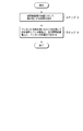
- FIG. 1 is a flowchart showing an example of a film forming method according to the first embodiment of the present invention.
- Sectional view showing an example of the state of the substrate Sectional view showing an example of the state of the substrate Sectional view showing an example of the state of the substrate Sectional view showing an example of the state of the substrate Sectional view showing a reference example
- the top view which shows roughly an example of the film-forming system which can implement an example of the film-forming method which concerns on 1st Embodiment of this invention
- Sectional drawing which shows an example of a processing unit roughly Sectional drawing which shows an example of a processing unit roughly Sectional view showing an example of the state of the substrate Sectional view showing an example of the state of the substrate Sectional view showing an example of the state of the substrate
- the top view which shows schematically an example of the film-forming system which can implement the other example of the film-forming method which concerns on 1st Embodiment of this invention
- the top view Sectional drawing which shows an example of a processing unit roughly Flow chart
- FIG. 1 is a flowchart showing an example of a film forming method according to the first embodiment of the present invention
- FIGS. 2A to 2D are sectional views showing examples of states of a substrate.
- FIG. 2A shows an example of the substrate 1.
- the substrate 1 according to an example is a semiconductor wafer, for example, a silicon wafer.
- 2A to 2D illustration of elements such as a silicon wafer and a transistor is omitted, and only wirings formed on the silicon wafer and an interlayer insulating film are schematically shown.
- an interlayer insulating film 2 is formed on a silicon wafer (not shown).
- a material example of the interlayer insulating film 2 is a silicon oxide insulating film.
- a groove for forming a wiring is formed in the interlayer insulating film 2, and a wiring 4 using copper is formed inside the groove.
- a barrier film 3 is formed around the wiring 4.
- a manganese-containing film is formed on the substrate 1 on which the wiring 4 using copper and the insulating film, in this example, the interlayer insulating film 2 are exposed.
- a manganese-containing film is formed as follows.
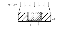
- the substrate 1 shown in FIG. 2A is carried into a processing container of a processing apparatus (not shown), and the surface of the interlayer insulating film 2 is made hydrophilic.
- the surface of the interlayer insulating film 2 is hydrophobized using a hydrophobizing substance having a hydrophobizing effect that hydrophobizes the surface of the interlayer insulating film 2.
- a non-hydrophilic region 5 is formed on the surface portion of the interlayer insulating film 2 (FIG. 2B).
- HMDS hexamethyldisilazane
- the hydrophilic “—OH group” is converted into hydrophobic “ ⁇ ” by HMDS. Substituted by “O—Si (CH 3 ) 3 ”. As a result, in this example, the non-hydrophilic region 5 is a hydrophobic region.
- An example of specific processing conditions is as follows.
- Step 2 in FIG. 1 manganese is contained on the wiring 4 using copper by using the CVD method using a manganese compound as a film forming gas for the substrate 1 shown in FIG. 2B. A film is formed.
- the manganese-containing film 6 is formed only on the wiring 4 using copper.
- the manganese-containing film 6 is a film containing manganese oxide, for example.
- Manganese oxide is produced by reacting with moisture in the base (in this specification, moisture is defined to include H 2 O and hydroxy (OH)). Therefore, the manganese-containing film 6 is hardly formed on the interlayer insulating film 2 in which the non-hydrophilic region 5 is formed, and is selectively formed only on the wiring 4 using copper (FIG. 2D).
- An example of specific processing conditions is as follows.
- the manganese-containing film 6 can be selectively formed only on the wiring 4 using copper without being formed on the interlayer insulating film 2. .
- the manganese-containing film 6, in particular, a film containing manganese oxide has a function of suppressing copper diffusion, and can be used as a barrier film for suppressing copper diffusion.
- the manganese-containing film 6 can be selectively formed only on the wiring 4 using copper, the manganese-containing film 6 is used as a so-called cap film. be able to.
- the manganese-containing film 6 is hardly formed on the interlayer insulating film 2 on which the non-hydrophilic region 5 is formed. This is because a manganese compound (EtCp) 2 Mn is used in this example, but since cyclopentadienyl (Cp) is aromatic and has ⁇ electrons, it is easily adsorbed on the Si—OH surface. This is probably because it is difficult to adsorb on the surface of —CH 3 .
- the manganese compound in addition to (EtCp) 2 Mn, if it is a manganese compound having a cyclopentadienyl-based ligand, the manganese-containing film 6 is formed on the interlayer insulating film 2 in which the non-hydrophilic region 5 is formed. It is possible to obtain the advantage that it is hardly formed.
- Examples of such manganese compounds include the following.
- TMDS (1,1,3,3-Tetramethyldisilazane)
- TMSDMA Dimethylaminotrimethylsilane
- DMSDMA Dimethylsilyldimethylamine
- TMMAS Trimethylmethylaminosilane
- TMICS Trimethyl (isocyanato) silane)
- TMSA Trimethylsilylacetylene
- TMSC Trimethylsilylcyanide
- the substrate 1 may be annealed and the interlayer insulating film 2 may be dehydrated in addition to the above-described hydrophobic treatment. Water is removed from the interlayer insulating film 2 by dehydrating the interlayer insulating film 2. Accordingly, moisture that oxidizes manganese can be almost eliminated from the interlayer insulating film 2, and growth of the manganese-containing film 6 on the interlayer insulating film 2 can be suppressed.
- the temperature of the substrate 1 is set higher than the temperature of the substrate 1 when the manganese-containing film 6 is formed.
- the temperature is sufficient to vaporize the water and the temperature range that can suppress the thermal history applied to the substrate 1 to a minimum is preferable.
- the temperature of the substrate 1 is set to a range of 100 ° C. or higher and 300 ° C. or lower, and the interlayer insulating film 2 is dehydrated.
- both the hydrophobization treatment and the dehydration treatment may be performed.
- the surface of the interlayer insulating film 2 is subjected to a hydrophobic treatment and the interlayer insulating film 2 is dehydrated, the growth of the manganese-containing film 6 on the interlayer insulating film 2 is more powerful. Can be suppressed.
- the hydrophobic treatment may be performed after the interlayer insulating film 2 is dehydrated.
- An example of the advantage that the manganese-containing film 6 can be selectively formed only on the wiring 4 using copper while hardly forming the manganese-containing film 6 on the interlayer insulating film 2 is, for example, as follows.
- FIG. 3 is a cross-sectional view showing a reference example.
- a CoWP film 7 is used as a cap film.
- CoWP is formed by an electroless plating method using the wiring 4 using copper as a catalyst. For this reason, the CoWP film 7 isotropically grows on the wiring 4 using copper.
- the CoWP film 7 expands in the lateral direction as the thickness of the CoWP film 7 increases.
- the CoWP film 7 is also formed on the interlayer insulating film 2.
- the CoWP film 7 is formed on the interlayer insulating film 2, there is a possibility that the CoWP films 7 are in contact with each other when the interval between the wirings 4 is narrow.
- the CoWP film 7 is conductive, when the CoWP films 7 are in contact with each other, the wirings 4 are short-circuited. Further, when copper removal is incomplete and a copper residue is formed on the interlayer insulating film 2, the CoWP film 7 is grown on the residue on the interlayer insulating film 2.
- the interlayer insulating film 2 is, for example, a low dielectric constant insulating film (Low-k film) whose material is weak
- the CoWP film 7 formed on the interlayer insulating film 2 is formed of the interlayer insulating film 2. There is a possibility of degrading the quality.
- the interlayer insulating film 2 is made of, for example, a low dielectric constant insulating film (Low- (k film), the possibility of degrading the quality of the interlayer insulating film 2 can be reduced as compared with the case where the CoWP film 7 is used as a cap film.
- Low- (k film) low dielectric constant insulating film
- the interval between the wirings 4 can be narrowed, for example, to be equal to or less than the interval at which the CoWP film 7 contacts. For this reason, the semiconductor device using the manganese-containing film 6 as a cap film is more advantageous for higher integration than the semiconductor device using the CoWP film 7 as a cap film.
- the first embodiment it is possible to provide a film forming method capable of forming a film that can be used as a cap film or a barrier film with good selective growth.
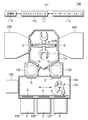
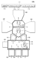
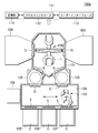
- FIG. 4 is a plan view schematically showing an example of a film forming system capable of carrying out an example of the film forming method according to the first embodiment of the present invention.
- the film forming system 100 includes a first processing unit 200 and a second processing unit 300.
- the processing units 200 and 300 are provided corresponding to two sides of the transfer chamber 101 having a polygonal shape, respectively.
- Load lock chambers 102 and 103 are provided on the other two sides of the transfer chamber 101, respectively.
- a loading / unloading chamber 104 is provided on the opposite side of the load lock chambers 102 and 103 from the transfer chamber 101.
- ports 105, 106, and 107 for attaching three carriers C that can accommodate the wafer W are provided on the opposite side of the loading / unloading chamber 104 from the load lock chambers 102 and 103.
- the processing units 200 and 300 and the load lock chambers 102 and 103 are connected to the transfer chamber 101 via a gate valve G.
- the processing units 200 and 300 and the load lock chambers 102 and 103 communicate with the transfer chamber 101 by opening the gate valve G, and are disconnected from the transfer chamber 101 by closing the gate valve G.
- the load lock chambers 102 and 103 are further connected to the carry-in / out chamber 104 via a gate valve G.
- the load lock chambers 102 and 103 communicate with the loading / unloading chamber 104 by opening the gate valve G, and are blocked from the loading / unloading chamber 104 by closing the corresponding gate valve G.
- a transfer device 108 that carries the substrate 1 in and out of the processing units 200 and 300 and the load lock chambers 102 and 103 is provided inside the transfer chamber 101.
- the transfer device 108 is disposed substantially at the center of the transfer chamber 101.
- the inside of the transfer chamber 101 is maintained at a predetermined degree of vacuum.
- the substrate 1 is transported between the processing units 200 and 300 and the load lock chambers 102 and 103 without being exposed to the atmosphere.
- a shutter S is provided in each of the ports 105, 106, and 107 of the carry-in / out chamber 104.
- the shutter S is released, and the carrier C communicates with the loading / unloading chamber 104 while preventing the intrusion of outside air.
- An alignment chamber 109 is provided on the side surface of the carry-in / out chamber 104. In the alignment chamber 109, the substrate 1 is aligned.
- a transfer device 110 that loads and unloads the substrate 1 with respect to the carrier C, the alignment chamber 109, and the load lock chambers 102 and 103 is provided.
- the control unit 111 controls the film forming system 100.
- the control unit 111 includes a process controller 112, a user interface 113, and a storage unit 114.
- the user interface 113 includes a keyboard on which a process manager inputs commands to manage the film forming system 100, a display that visualizes and displays the operating status of the film forming system 100, and the like.
- the storage unit 114 stores a recipe that records a control program, drive condition data, and the like for realizing the processing by the film forming system 100 under the control of the process controller 112.
- the recipe is called from the storage unit 114 by an instruction from the user interface 113 as necessary, and the film forming system 100 is controlled by causing the process controller 112 to execute the recipe.
- a recipe stored in a computer-readable storage medium such as a CD-ROM, a hard disk, or a flash memory may be used, or may be transmitted from another device at any time via a dedicated line, for example. It is also possible to use it.
- the first processing unit 200 is a device that performs a process of making the surface of the interlayer insulating film 2 non-hydrophilic.
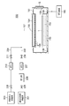
- FIG. 5 is a cross-sectional view schematically showing an example of the processing unit 200.
- the processing unit 200 includes a processing container 151 that accommodates the substrate 1 and can be held in a vacuum.
- a susceptor 152 on which the substrate 1 is placed is provided at the bottom of the processing container 151.
- a heater 153 that heats the substrate 1 is embedded in the susceptor 152.
- a shower head 154 facing the susceptor 152 is provided on the upper portion of the processing container 151.
- the shower head 154 has a gas inlet 155 at the center of the upper surface and a plurality of gas discharge holes 156 on the lower surface.
- a gas supply pipe 157 is connected to the gas inlet 155.
- the gas supply pipe 157 includes a pipe 202 extending from a hydrophobizing substance supply source 201 that supplies a hydrophobizing substance such as HMDS, and a pipe extending from a dilution gas supply source 203 that supplies a dilution gas composed of Ar gas, N 2 gas, or the like. 204 is connected.
- the pipe 202 is provided with a valve 205, a vaporizer 206, a mass flow controller 207, and a valve 208 for vaporizing the hydrophobic substance, in this example, HMDS, in this order from the hydrophobic substance supply source 201 side.
- the pipe 204 is provided with a valve 209, a mass flow controller 210, and a valve 211 in order from the dilution gas supply source 203 side.
- the hydrophobized substance is vaporized by the vaporizer 206 and introduced into the processing vessel 151 through the gas supply pipe 157 and the shower head 154 in a state where the vaporized hydrophobized substance is diluted with a diluent gas. Is done.
- the substrate 1 is heated to a predetermined temperature by the heater 153. In this example, the temperature of the substrate 1 can be controlled from room temperature to 300 ° C., for example.
- a loading / unloading port 158 for loading / unloading the substrate 1 is provided on the side wall of the processing container 151.
- the loading / unloading port 158 can be opened and closed by a gate valve G.
- An exhaust port 159 is provided at the bottom of the processing container 151.
- An exhaust device 160 is connected to the exhaust port 159.
- the pressure inside the processing container 151 can be reduced to a predetermined degree of vacuum by exhausting with the exhaust device 160.
- the exhaust port 159 may not be connected to the exhaust device 160, and the pressure inside the processing container 151 may be maintained at atmospheric pressure.
- the second processing unit 300 is an apparatus that forms a manganese-containing film on a wiring that uses copper.
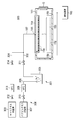
- FIG. 6 is a cross-sectional view schematically showing an example of the processing unit 300.
- the processing unit 300 of this example is configured as a thermal CVD apparatus for forming a manganese-containing film, and includes a processing container 151 and a susceptor 152 similar to those of the processing unit 200.
- a heater 153 is embedded in the susceptor 152 so that the substrate 1 can be heated to, for example, room temperature to 100 ° C. Since the other configuration is substantially the same as the configuration of the processing unit 200, only different parts will be described below.
- the gas supply pipe 157 includes a pipe 302 extending from a manganese compound supply source 301 that supplies a manganese compound such as (EtCp) 2 Mn, and a carrier gas supply source 303 that supplies a carrier gas made of Ar gas, N 2 gas, or the like.
- An extending pipe 304 is connected.
- the manganese compound supply source 301 includes a manganese compound reservoir 305 in this example.
- (EtCp) 2 Mn is stored in the manganese compound storage unit 305 as a manganese compound in a liquid state.
- a bubbling mechanism 306 is connected to the manganese compound reservoir 305.
- the bubbling mechanism 306 adjusts the bubbling gas reservoir 307 in which bubbling gas is stored, the supply pipe 308 that guides the bubbling gas to the manganese compound reservoir 305, and the flow rate of the bubbling gas that flows through the supply pipe 308.
- a mass flow controller 309 and a valve 310 are included.
- the bubbling gas include argon (Ar) gas, hydrogen (H 2 ) gas, and nitrogen (N 2 ) gas.
- One end of the supply pipe 308 is disposed in the manganese compound liquid stored in the manganese compound storage unit 305, in this example, (EtCp) 2 Mn. By blowing the bubbling gas from the supply pipe 308, the manganese compound liquid is bubbled and vaporized.
- the vaporized manganese compound gas, (EtCp) 2 Mn gas in this example passes through the pipe 302 and the valve 311 that opens and closes the pipe 302, passes through the gas supply pipe 157 and the shower head 154, and enters the processing container 151. be introduced.
- a pipe 304 is connected to the gas supply pipe 157, and a carrier gas is introduced from the carrier gas supply source 303 through the valve 312, the mass flow controller 313, and the valve 314.
- An example of a film forming method according to the first embodiment of the present invention uses a film forming system 100 as shown in FIGS. 4 to 6, and the processing unit 200 is hydrophilic to the surface of the interlayer insulating film 2.
- the substrate 1 subjected to this treatment is transferred to the processing unit 300 through the transfer chamber 101 without being exposed to the atmosphere, and the processing unit 300 uses the copper on the wiring that uses copper. It can be carried out by forming a manganese-containing film.
- FIGS. 7A to 7C are cross-sectional views showing examples of the state of the substrate.
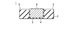
- the surface of the interlayer insulating film 2 when the surface of the interlayer insulating film 2 is subjected to a treatment for making it non-hydrophilic, the surface of the wiring 4 using copper is hydrophobized as shown in FIG. 7B.
- Substances and / or oxides 8 may be deposited or formed. In this case, it is preferable to remove the hydrophobic substance and / or oxide 8 on the surface of the wiring 4 using copper while maintaining that the surface of the interlayer insulating film 2 is not hydrophilic. .
- the hydrophobic substance and / or oxide 8 on the surface of the wiring 4 using copper is removed using an organic compound while maintaining that the surface of the interlayer insulating film 2 is not hydrophilic.
- an organic acid containing a carboxylic acid such as formic acid (HCOOH) was used as the organic compound.
- HCOOH formic acid
- the hydrophobic substance and / or the oxide 8 attached or formed on the surface of the wiring 4 using copper can be removed using an organic compound. Moreover, according to the removal using the organic compound, the surface of the wiring 4 using copper is applied to the hydrophobizing substance and / or the oxide 8 while maintaining that the surface of the interlayer insulating film 2 is not hydrophilic. It can be removed from above. Then, after removing the hydrophobic substance and / or the oxide 8 from the surface of the wiring 4 using copper, the manganese-containing film is formed on the surface of the wiring 4 using copper as described above. 6 may be formed.
- the hydrophobic substance and / or the oxide 8 is removed from the surface of the wiring 4 using copper, so that the wiring 4 is brought into contact with the other wiring connected to the wiring 4. An increase in resistance or the like can be suppressed.
- Examples include alcohols having a hydroxy group (—OH), aldehydes having an aldehyde group (—CHO), carboxylic acids having a carboxyl group (—COOH), carboxylic acid anhydride esters, and ketones, and at least one of these may be used. it can.
- R 1 is a linear or branched C1-C20 alkyl or alkenyl group, preferably methyl, ethyl, propyl, butyl, pentyl or hexyl
- R 2 —CH—R 3 R 2 and R 3 are linear or branched C1-C20 alkyl or alkenyl groups, preferably methyl, ethyl, propyl, butyl, pentyl or hexyl
- R 2 —CH—R 3 R 2 and R 3 are linear or branched C1-C20 alkyl or alkenyl groups, preferably methyl, ethyl, propyl, butyl, pentyl or hexyl
- R 2 —CH—R 3 R 2 and R 3 are linear or branched C1-C20 alkyl or alkenyl groups, preferably methyl, ethyl, propyl, butyl, pentyl or hexyl
- R 4 -CHO (3) R 4 is hydrogen, or a linear or branched C1-C20 alkyl or alkenyl group, preferably methyl, ethyl, propyl, butyl, pentyl or hexyl
- An aldehyde having For example, formaldehyde (HCHO) Acetaldehyde (CH 3 CHO) Propionaldehyde (CH 3 CH 2 CHO), and butyraldehyde (CH 3 CH 2 CH 2 CHO ) 2
- HCHO formaldehyde
- CH 3 CHO Propionaldehyde
- butyraldehyde CH 3 CH 2 CH 2 CHO
- OHC-R 5 -CHO (4) R 5 is a linear or branched C1-C20 saturated or unsaturated hydrocarbon, but R 5 is not present, ie, both aldehyde groups may be bonded to each other
- alkanediol compounds having the following.
- R 6 is hydrogen, or a linear or branched C1-C20 alkyl or alkenyl group, preferably methyl, ethyl, propyl, butyl, pentyl or hexyl
- a carboxylic acid having For example, formic acid (HCOOH) Acetic acid (CH 3 COOH) Propionic acid (CH 3 CH 2 COOH) Butyric acid (CH 3 (CH 2 ) 2 COOH) and Valeric acid (CH 3 (CH 2 ) 3 COOH) Etc.
- Carboxylic anhydride has the following general formula (6) R 7 —CO—O—CO—R 8 (6) (R 7 and R 8 are a hydrogen atom, a hydrocarbon group, or a functional group in which at least part of the hydrogen atoms constituting the hydrocarbon group are substituted with halogen atoms) Can be defined as
- an alkyl group, an alkenyl group, an alkynyl group, an allyl group, and the like can be mentioned.
- Specific examples of the halogen atom include: Fluorine, chlorine, bromine, and iodine.
- carboxylic anhydride in addition to acetic anhydride, Formic anhydride, propionic anhydride, acetic formic anhydride, butyric anhydride, and valeric anhydride.
- the ester has the following general formula (7) R 9 -COO-R 10 (7)
- R 9 is a hydrogen atom, a hydrocarbon group or a functional group in which at least a part of the hydrogen atoms constituting the hydrocarbon group is substituted with a halogen atom
- R 10 is a hydrogen atom constituting a hydrocarbon group or a hydrocarbon group A functional group in which at least a part of is substituted with a halogen atom).
- hydrocarbon group and the halogen atom are the same as those described above.
- esters include Methyl formate ethyl oxalate propyl formate butyl formate benzyl acetate methyl acetate ethyl acetate propyl acetate butyl acetate pentyl acetate hexyl acetate octyl acetate phenyl acetate benzyl acetate allyl acetate propenyl acetate propionate methyl propionate butyl propionate pentyl propionate benzyl methyl butyrate
- Examples include ethyl butyrate, pentyl butyrate, butyl butyrate, methyl valerate, and ethyl valerate.
- FIG. 8 is a plan view schematically showing an example of a film forming system capable of carrying out another example of the film forming method according to the first embodiment of the present invention.
- the film forming system 100a is different from the film forming system 100 in that a third processing unit 400 is further provided.
- the third processing unit 400 is connected to the transfer chamber 101 via the gate valve G.
- the third processing unit 400 is an apparatus for removing the hydrophobic substance and / or the oxide 8 on the surface of the wiring 4 using copper while maintaining that the surface of the interlayer insulating film 2 is not hydrophilic. It is.
- FIG. 9 is a cross-sectional view schematically showing an example of the processing unit 400.
- the processing unit 400 has substantially the same configuration as the processing units 200 and 300. Only different parts will be described below.
- the gas supply pipe 157 includes a pipe 402 extending from an organic compound supply source 401 that supplies an organic compound.
- the organic compound supply source 401 includes an organic compound reservoir 403 in this example.
- formic acid HCOOH
- HCOOH formic acid
- the vaporized HCOOH gas passes through the gas supply pipe 157 and the shower head 154 through the pipe 402, the valve 405 that opens and closes the pipe 402, the mass flow controller 406, and the valve 407 that also opens and closes the pipe 402. To be introduced.
- the heater 404 is configured to heat the gas supply pipe 157, the pipe 402, the valves 405 and 407, and the mass flow controller 406 in addition to the organic compound reservoir 403.
- the organic compound supply source 401 may be provided with a dilution gas supply mechanism for supplying a dilution gas for diluting the organic compound gas.
- a dilution gas is nitrogen (N 2 ) gas.
- FIG. 8 and FIG. 8 Another example of the film forming method according to the first embodiment of the present invention uses a film forming system 100a as shown in FIG. 8 and FIG.
- the substrate 1 that has been subjected to the treatment for making it non-hydrophilic is transferred to the processing unit 400 through the transfer chamber 101 without being exposed to the atmosphere, and the surface of the interlayer insulating film 2 is not hydrophilic. While maintaining, the hydrophobic substance and / or oxide 8 on the surface of the wiring 4 using copper is removed, and the substrate 1 subjected to this treatment is exposed to the atmosphere through the transfer chamber 101.
- it can be carried out by forming a manganese-containing film on the wiring 4 that is transported to the processing unit 300 and uses copper in the processing unit 300.
- FIG. 10 is a flowchart showing an example of a film forming method according to the second embodiment of the present invention
- FIGS. 11A to 11D are cross-sectional views showing examples of states of the substrate.
- FIG. 11A shows an example of the substrate 1.
- substrate 1 which concerns on an example is the structure similar to the board
- a manganese-containing film is formed on both the wiring 4 using copper and the interlayer insulating film 2 as follows.
- the substrate 1 shown in FIG. 11A is carried into a processing container of a processing apparatus (not shown), and the surface of the interlayer insulating film 2 is made hydrophilic. .
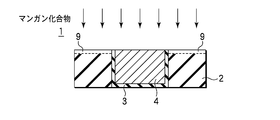
- the surface of the interlayer insulating film 2 is subjected to plasma treatment, and a damaged layer 9 is formed on the surface of the interlayer insulating film 2 (FIG. 11B).
- a damaged layer 9 is formed on the surface of the interlayer insulating film 2 (FIG. 11B).
- a hydrophobic substance is removed, and the surface of the interlayer insulating film 2 is hydrophilized.
- An example of the plasma treatment is to expose the substrate 1 to a plasma containing hydrogen (H).
- An example of specific processing conditions is as follows.
- Processing container pressure 1 Pa to 1000 Pa
- Substrate temperature Room temperature to 300 ° C
- Atmosphere in processing container H 2 atmosphere
- Processing time 1sec or more and 600sec or less
- Step 4 in FIG. 10 on the substrate 1 shown in FIG. 11B, on the surface of the wiring 4 using copper by using the CVD method using a manganese compound as a film forming gas, and on the surface A manganese-containing film is formed on the interlayer insulating film 2 that has been hydrophilized.
- the manganese-containing film 6 is formed on both the wiring 4 using copper and the interlayer insulating film 2.
- the manganese-containing film 6 is a film containing manganese oxide, for example.
- Manganese oxide is produced by reacting with the underlying moisture.
- the surface of the interlayer insulating film 2 is hydrophilized, so that the manganese-containing film 6 can also be formed on the interlayer insulating film 2.
- An example of specific processing conditions is as follows.
- Processing container pressure 1 Pa to 1000 Pa
- Substrate temperature 50 ° C or higher and 400 ° C or lower
- Atmosphere in processing container (EtCp) 2 Mn atmosphere
- Processing time 1sec or more and 600sec or less
- moisture may be adsorbed on the surface of the hydrophilic interlayer insulating film 2.
- the surface of the interlayer insulating film 2 is made hydrophilic so that the manganese-containing film 6 is formed on the wiring 4 and the interlayer insulating film 2 using copper. It is possible to form both.
- the manganese-containing film 6 can be formed so that the film thickness t4 on the wiring 4 and the film thickness t2 on the interlayer insulating film 2 are approximately the same. For this purpose, for example, the amount of moisture present on the surface of the interlayer insulating film 2 may be controlled.
- the manganese-containing film 6, particularly a film containing manganese oxide has a function of suppressing copper diffusion.
- the manganese-containing film 6 formed according to the example of the second embodiment can be used as a barrier film that suppresses the diffusion of copper.
- FIG. 12 is a plan view schematically showing an example of a film forming system capable of carrying out an example of a film forming method according to the second embodiment of the present invention.
- the film forming system 100 b is different from the film forming system 100 in that a fourth processing unit 500 is provided instead of the first processing unit 200.
- the fourth processing unit 500 is connected to the transfer chamber 101 via the gate valve G.
- the fourth processing unit 500 is a device that performs hydrophilic processing on the surface of the interlayer insulating film 2.
- FIG. 13 is a cross-sectional view schematically showing an example of the processing unit 500.
- the processing unit 500 is configured as a parallel plate type plasma apparatus.
- the processing unit 500 is different from the processing units 200, 300, and 400 in that the susceptor 152 is insulated from the processing container 151 by the insulator 161, and a high frequency power supply 162 that supplies high frequency power to the susceptor 152 is connected.
- the shower head 154 is grounded and is configured to be a counter electrode when the susceptor 152 is used as one electrode, and a plasma generation gas supply source 501 for supplying a plasma generation gas to the gas supply pipe 157.
- a pipe 502 extending from the pipe is connected.
- the pipe 502 is provided with a valve 503, a mass flow controller 504, and a valve 505 in order from the plasma generation gas supply source 501 side.
- the plasma generating gas is introduced into the processing vessel 151 through the pipe 502, valves 503 and 505 for opening and closing the pipe 502, the mass flow controller 504, the gas supply pipe 157, and the shower head 154.
- the plasma generating gas include a gas containing hydrogen, a gas containing carbon, a gas containing nitrogen, a gas containing oxygen, a gas containing a halogen element, and a gas containing a rare gas.
- An example of a film forming method according to the second embodiment of the present invention uses a film forming system 100b as shown in FIGS. 12 and 13, and the processing unit 500 is hydrophilic to the surface of the interlayer insulating film 2.
- the substrate 1 subjected to this process is transferred to the processing unit 300 through the transfer chamber 101 without being exposed to the atmosphere, and the wiring 4 that uses copper in the processing unit 300 is used. This can be implemented by forming a manganese-containing film on the interlayer insulating film 2.
- an example is shown in which the surface of the interlayer insulating film 2 is subjected to plasma processing as a process for making the surface of the interlayer insulating film 2 hydrophilic, and the damaged layer 9 is formed. It is possible to use a method of forming a damaged layer 9 by performing an ultraviolet ozone treatment in which ozone generated by ultraviolet irradiation is brought into contact with the surface, and a method of adsorbing moisture on the surface of the interlayer insulating film 2.
- FIGS. 14A to 14C are cross-sectional views showing examples of the state of the substrate.
- the oxide 10 is formed on the surface of the wiring 4 using copper as shown in FIG. 14B. May be formed. In this case, it is preferable to remove the oxide on the surface of the wiring 4 using copper while maintaining that the surface of the interlayer insulating film 2 is hydrophilic.
- the oxide 10 on the surface of the wiring 4 using copper was removed using an organic compound while maintaining the surface of the interlayer insulating film 2 to be hydrophilic (FIG. 14C).
- an organic acid containing a carboxylic acid such as formic acid (HCOOH) was used as the organic compound.
- HCOOH formic acid
- the oxide 10 formed on the surface of the wiring 4 using copper can be removed using an organic compound. Moreover, according to the removal using the organic compound, the oxide 10 can be removed from the surface of the wiring 4 using copper while maintaining the surface of the interlayer insulating film 2 being hydrophilic. it can. Then, after removing the oxide 10 from the surface of the wiring 4 using copper, the manganese-containing film 6 is formed on the surface of the wiring 4 using copper and the interlayer insulating film 2 as described above. Should be formed.
- organic compound that can be used in the film forming method according to another example is the same as the organic compound described in the first embodiment.
- processing unit 400 shown in FIG. 9 can be used as the processing unit. That is, as the film forming system, the processing unit 400 may be further connected to the film forming system 100b shown in FIG.
- the surface of the interlayer insulating film 2 is subjected to a hydrophilic process in the processing unit 500, and the substrate 1 subjected to this process is processed.
- Oxide on the surface of the wiring 4 using copper while being transferred to the processing unit 400 without being exposed to the atmosphere through the transfer chamber 101 and maintaining the surface of the interlayer insulating film 2 being hydrophilic. 10 is removed and the processed substrate 1 is transferred to the processing unit 300 through the transfer chamber 101 without being exposed to the atmosphere, and the processing unit 300 uses copper on the wiring 4 and interlayer insulation. This can be done by forming a manganese-containing film on the film 2.
- a cleaning method using an organic compound is used to remove the oxide 10, but a hydrogen annealing method and an extremely low oxygen partial pressure method can also be used to remove the oxide 10.
- the film forming method according to the embodiment of the present invention it is possible to select whether to form a cap film or a film that can be used as a barrier film. Can provide a method.
- the surface of the interlayer insulating film is made non-hydrophilic with respect to the surface of the interlayer insulating film, for example, hydrophobic Treatment or dehydration treatment was performed.
- hydrophobic Treatment or dehydration treatment was performed.
- the surface of the non-hydrophilic interlayer insulating film is further subjected to a treatment for making it non-hydrophilic, for example, a hydrophobic treatment or a dehydration treatment. Also good. In this case, it is possible to obtain an advantage that the growth of the manganese-containing film on the interlayer insulating film can be more strongly suppressed.
- the surface of the interlayer insulating film is made hydrophilic with respect to the surface of the interlayer insulating film, for example, plasma processing. Or ultraviolet ozone treatment or moisture adsorption treatment.
- a hydrophilic material as the material of the interlayer insulating film. In this case, the hydrophilic treatment can be omitted, and the advantage that it is advantageous for improving the throughput can be obtained.
- the hydrophilic surface of the interlayer insulating film is made hydrophilic, for example, plasma treatment, ultraviolet ozone treatment, or moisture adsorption. Processing may be further performed. In this case, the advantage that the growth of the manganese-containing film on the interlayer insulating film can be more strongly promoted can be obtained.
- barrier film 3 tantalum (Ta), titanium (Ti), and nitrides thereof are conventionally used, but the same manganese-containing film as the manganese-containing film 6 of the present invention is used.
- tantalum (Ta), titanium (Ti), and nitrides thereof are conventionally used, but the same manganese-containing film as the manganese-containing film 6 of the present invention is used.
- the present invention it is possible to provide a film forming method capable of selecting whether or not to form a film that can be used as a cap film or a barrier film.
Landscapes
- Chemical & Material Sciences (AREA)
- General Chemical & Material Sciences (AREA)
- Chemical Kinetics & Catalysis (AREA)
- Engineering & Computer Science (AREA)
- Materials Engineering (AREA)
- Mechanical Engineering (AREA)
- Metallurgy (AREA)
- Organic Chemistry (AREA)
- Inorganic Chemistry (AREA)
- Internal Circuitry In Semiconductor Integrated Circuit Devices (AREA)
- Chemical Vapour Deposition (AREA)
- Electrodes Of Semiconductors (AREA)
- Formation Of Insulating Films (AREA)
Abstract
Description
(成膜方法の一例)
図1はこの発明の第1の実施形態に係る成膜方法の一例を示す流れ図、図2A~図2Dは基板の状態例を示す断面図である。
基板温度 : 室温以上300℃以下
処理容器内雰囲気: HMDS雰囲気
処理時間 : 1sec以上600sec以下
次に、図1中のステップ2に示すように、図2Bに示す基板1に対して、マンガン化合物を成膜ガスとするCVD法を用いて、銅を使用している配線4上にマンガン含有膜を形成する。本例では一例として、マンガン化合物としてビスエチルシクロペンタジエニルマンガン((EtCp)2Mn[=Mn(C2H5C5H4)2])を成膜ガスとする熱CVD法を用いた(図2C)。このような処理により、本例では、銅を使用している配線4上のみにマンガン含有膜6が形成される。マンガン含有膜6は、例えば、マンガン酸化物を含む膜である。マンガン酸化物は、下地の水分(本明細書では水分とはH2O、及びヒドロキシ(OH)を含むと定義する)と反応して生成される。このため、マンガン含有膜6は、親水性でない領域5が形成された層間絶縁膜2上にはほとんど形成されず、銅を使用している配線4上のみに選択的に形成される(図2D)。具体的な処理条件の一例は以下の通りである。
基板温度 : 50℃以上400℃以下
処理容器内雰囲気: (EtCp)2Mn雰囲気
処理時間 : 1sec以上600sec以下
このような第1の実施形態によれば、マンガン含有膜6を、層間絶縁膜2上にはほとんど形成せずに、銅を使用している配線4上のみに選択的に形成することができる。
Cp2Mn[=Mn(C5H5)2]
(MeCp)2Mn[=Mn(CH3C5H4)2]
(i-PrCp)2Mn[=Mn(C3H7C5H4)2]
MeCpMn(CO)3[=(CH3C5H4)Mn(CO)3]
(t-BuCp)2Mn[=Mn(C4H9C5H4)2]
Mn(DMPD)(EtCp)[=Mn(C7H11C2H5C5H4)]、及び
((CH3)5Cp)2Mn[=Mn((CH3)5C5H4)2]
また、層間絶縁膜2の表面を疎水化させる疎水化効果を有する疎水化物質としては、HMDSの他、以下のシリコン含有有機化合物を挙げることができる。
TMSDMA(Dimethylaminotrimethylsilane)
DMSDMA(Dimethylsilyldimethylamine)
TMMAS(Trimethylmethylaminosilane)
TMICS(Trimethyl(isocyanato)silane)
TMSA(Trimethylsilylacetylene)、及び
TMSC(Trimethylsilylcyanide)
1,3,5,7-テトラメチルシクロテトラシロキサン
ジメチルシラン
テトラエチルシクロテトラシロキサン
1,2,3-トリエチル-2,4,6-トリメチルシクロトリシラザン
1,2,3,4,5,6-ヘキサメチルシクロトリシラザン
モノメチルシラン
ヘキサメチルジシラン
ヘキサメチルシロキサン
トリメチルシラン
テトラメチルシラン
ジメチルジメトキシシラン
オクタメチルシクロテトラシロキサン
トリメトキシメチルシラン
ヘキサエチルジシラザン
ヘキサフェニルジシラザン
ヘプタメチルジシラザン
ジプロピル-テトラメチルジシラザン
ジ-n-ブチル-テトラメチルジシラザン
ジ-n-オクチル-テトラメチルジシラザン
ジビニル-テトラメチルジシラザン
1,1,3,3,5,5-ヘキサメチルシクロトリシラザン
ヘキサエチルシクロトリシラザン
ヘキサフェニルシクロトリシラザン
オクタメチルシクロテトラシラザン
オクタエチルシクロテトラシラザン
テトラエチル-テトラメチルシクロテトラシラザン
テトラフェニルジメチルジシラザン
ジフェニル-テトラメチルジシラザン
トリビニル-トリメチルシクロトリシラザン、及び
テトラビニル-テトラメチルシクロテトラシラザン
また、マンガン含有膜6、特に、マンガン酸化物を含む膜は、下地の水分と反応することで生成される。このため、層間絶縁膜2の表面に対して、親水性でなくする処理としては、上述した疎水化処理の他、基板1をアニールし、層間絶縁膜2を脱水処理するようにしても良い。層間絶縁膜2を脱水処理することで、層間絶縁膜2から水分が除去される。これにより、マンガンを酸化させる水分を、層間絶縁膜2からほとんど無くすことができ、マンガン含有膜6の層間絶縁膜2上への成長を抑制することができる。基板1のアニールの例としては、基板1の温度を、マンガン含有膜6を形成する際の基板1の温度よりも高くすることである。この際、水分を気化させるのに充分な温度、かつ、基板1に与えられる熱履歴を最小限度に抑制できる温度の範囲で行うことが良い。具体的な一例は、例えば、基板1の温度を、100℃以上300℃以下の範囲として、層間絶縁膜2を脱水処理する。
(成膜システム)
図4は、この発明の第1の実施形態に係る成膜方法の一例を実施することが可能な成膜システムの一例を概略的に示す平面図である。
第1の処理ユニット200は、層間絶縁膜2の表面に対して、親水性でなくする処理を施す装置である。
第2の処理ユニット300は、銅を使用している配線上に、マンガン含有膜を成膜する装置である。
図7A~図7Cは、基板の状態例を示す断面図である。
基板温度 : 100℃以上300℃以下
処理容器内雰囲気: HCOOH雰囲気
処理時間 : 1sec以上600sec以下
このように、銅を使用している配線4の表面上に付着、又は形成された疎水化物質、及び/又は酸化物8は、有機化合物を用いて除去することができる。しかも、有機化合物を用いた除去によれば、層間絶縁膜2の表面が親水性でないことを維持しつつ、疎水化物質、及び/又は酸化物8を、銅を使用している配線4の表面上から除去することができる。そして、疎水化物質、及び/又は酸化物8を、銅を使用している配線4の表面上から除去した後、銅を使用している配線4の表面上に、上述したようにマンガン含有膜6を形成すれば良い。
ヒドロキシ基(-OH)を有するアルコール
アルデヒド基(-CHO)を有するアルデヒド
カルボキシル基(-COOH)を有するカルボン酸
無水カルボン酸
エステル、及び
ケトンを挙げることができ、これらの少なくとも1種を用いることができる。
1)第1級アルコール、特に以下の一般式(1)
R1-OH ・・・(1)
(R1は直鎖または分枝鎖状のC1~C20のアルキル基またはアルケニル基、好ましくはメチル、エチル、プロピル、ブチル、ペンチルまたはヘキシル)
を有する第1級アルコール、
例えば、メタノール(CH3OH)
エタノール(CH3CH2OH)
プロパノール(CH3CH2CH2OH)
ブタノール(CH3CH2CH2CH2OH)
2-メチルプロパノール((CH3)2CHCH2OH)、及び
2-メチルブタノール(CH3CH2CH(CH3)CH2OH)
2)第2級アルコール、特に以下の一般式(2)
OH
| ・・・(2)
R2-CH-R3
(R2、R3は直鎖または分枝鎖状のC1~C20のアルキル基またはアルケニル基、好ましくはメチル、エチル、プロピル、ブチル、ペンチルまたはヘキシル)
を有する第2級アルコール、
例えば、2-プロパノール((CH3)2CHOH)
2-ブタノール(CH3CH(OH)CH2CH3)
3)ジオールおよびトリオールのようなポリヒドロキシアルコール
例えば、エチレングリコール(HOCH2CH2OH)
グリセロール(HOCH2CH(OH)CH2OH)
4)1~10個、典型的には5~6個の炭素原子を環の一部に有する環状アルコール
5)ベンジルアルコール(C6H5CH2OH)、o-、p-またはm-クレゾール、レゾルシノール等の芳香族アルコール
などが挙げられる。
1)以下の一般式(3)
R4-CHO ・・・(3)
(R4は水素、または直鎖もしくは分枝鎖状のC1~C20のアルキル基もしくはアルケニル基、好ましくはメチル、エチル、プロピル、ブチル、ペンチルまたはヘキシル)
を有するアルデヒド、
例えば、ホルムアルデヒド(HCHO)
アセトアルデヒド(CH3CHO)
プロピオンアルデヒド(CH3CH2CHO)、及び
ブチルアルデヒド(CH3CH2CH2CHO)
2)以下の一般式(4)
OHC-R5-CHO ・・・(4)
(R5は直鎖または分枝鎖状のC1~C20の飽和または不飽和炭化水素であるが、R5が存在しないこと、すなわち両アルデヒド基が互いに結合していることも可能)
を有するアルカンジオール化合物
などが挙げられる。
1)以下の一般式(5)
R6-COOH ・・・(5)
(R6は水素、または直鎖もしくは分枝鎖状のC1~C20のアルキル基もしくはアルケニル基、好ましくはメチル、エチル、プロピル、ブチル、ペンチルまたはヘキシル)
を有するカルボン酸、
例えば、蟻酸(HCOOH)
酢酸(CH3COOH)
プロピオン酸(CH3CH2COOH)
酪酸(CH3(CH2)2COOH)、及び
吉草酸(CH3(CH2)3COOH)
などが挙げられる。
R7-CO-O-CO-R8 ・・・(6)
(R7、R8は、水素原子または炭化水素基または炭化水素基を構成する水素原子の少なくとも一部がハロゲン原子に置換された官能基)
で表記されるものと定義することができる。
アルキル基
アルケニル基
アルキニル基、及び
アリル基
などを挙げることができ、ハロゲン原子の具体例としては、
フッ素
塩素
臭素、及び
ヨウ素
などを挙げることができる。
無水蟻酸
無水プロピオン酸
無水酢酸蟻酸
無水酪酸、及び
無水吉草酸
などを挙げることができる。
R9-COO-R10 ・・・(7)
(R9は、水素原子または炭化水素基または炭化水素基を構成する水素原子の少なくとも一部がハロゲン原子に置換された官能基、R10は、炭化水素基または炭化水素基を構成する水素原子の少なくとも一部がハロゲン原子に置換された官能基)と表記されるものと定義することができる。
蟻酸メチル
蛾酸エチル
蟻酸プロピル
蟻酸ブチル
蟻酸ベンジル
酢酸メチル
酢酸エチル
酢酸プロピル
酢酸ブチル
酢酸ペンチル
酢酸ヘキシル
酢酸オクチル
酢酸フェニル
酢酸ベンジル
酢酸アリル
酢酸プロペニル
プロピオン酸メチル
プロピオン酸エチル
プロピオン酸ブチル
プロピオン酸ペンチル
プロピオン酸ベンジル
酪酸メチル
酪酸エチル
酪酸ペンチル
酪酸ブチル
吉草酸メチル、及び
吉草酸エチル
などを挙げることができる。
(成膜システム)
図8は、この発明の第1の実施形態に係る成膜方法の他例を実施することが可能な成膜システムの一例を概略的に示す平面図である。
第3の処理ユニット400は、層間絶縁膜2の表面が親水性でないことを維持しつつ、銅を使用している配線4の表面上の疎水化物質、及び/又は酸化物8を除去する装置である。
(成膜方法の一例)
図10はこの発明の第2の実施形態に係る成膜方法の一例を示す流れ図、図11A~図11Dは基板の状態例を示す断面図である。
基板温度 : 室温以上300℃以下
処理容器内雰囲気: H2雰囲気
処理時間 : 1sec以上600sec以下
次に、図10中のステップ4に示すように、図11Bに示す基板1に対して、マンガン化合物を成膜ガスとするCVD法を用いて、銅を使用している配線4上、及び表面が親水化された層間絶縁膜2上にマンガン含有膜を形成する。本例では一例として、マンガン化合物としてビスエチルシクロペンタジエニルマンガン((EtCp)2Mn[=Mn(C2H5C5H4)2])を成膜ガスとする熱CVD法を用いた(図11C)。このような処理により、本例では、銅を使用している配線4上と層間絶縁膜2上との双方にマンガン含有膜6が形成される。マンガン含有膜6は、例えば、マンガン酸化物を含む膜である。マンガン酸化物は、下地の水分と反応して生成されるが、本例では層間絶縁膜2の表面が親水化されているため、マンガン含有膜6は層間絶縁膜2上にも形成することができる(図11D)。具体的な処理条件の一例は以下の通りである。
基板温度 : 50℃以上400℃以下
処理容器内雰囲気: (EtCp)2Mn雰囲気
処理時間 : 1sec以上600sec以下
なお、マンガン含有膜6を、より効率良く層間絶縁膜2上に形成するためには、親水化された層間絶縁膜2の表面に、水分を吸着させておくことも良い。
(成膜システム)
図12は、この発明の第2の実施形態に係る成膜方法の一例を実施することが可能な成膜システムの一例を概略的に示す平面図である。
第4の処理ユニット500は、層間絶縁膜2の表面に対して、親水性とする処理を施す装置である。
図14A~図14Cは、基板の状態例を示す断面図である。
基板温度 : 100℃以上300℃以下
処理容器内雰囲気: HCOOH雰囲気
処理時間 : 1sec以上600sec以下
このように、銅を使用している配線4の表面上に形成された酸化物10は、有機化合物を用いて除去することができる。しかも、有機化合物を用いた除去によれば、層間絶縁膜2の表面が親水性であることを維持しつつ、酸化物10を、銅を使用している配線4の表面上から除去することができる。そして、酸化物10を、銅を使用している配線4の表面上から除去した後、銅を使用している配線4の表面上及び層間絶縁膜2上に、上述したようにマンガン含有膜6を形成すれば良い。
Claims (19)
- 銅を使用している配線と絶縁膜とが表面に露出している基板に対してマンガン含有膜を成膜する成膜方法であって、
(1)銅を使用している配線上に、前記マンガン化合物を用いたCVD法を用いて前記マンガン含有膜を形成する工程を備える成膜方法。 - 前記マンガン化合物が、
(EtCp)2Mn[=Mn(C2H5C5H4)2]
Cp2Mn[=Mn(C5H5)2]
(MeCp)2Mn[=Mn(CH3C5H4)2]
(i-PrCp)2Mn[=Mn(C3H7C5H4)2]
MeCpMn(CO)3[=(CH3C5H4)Mn(CO)3]
(t-BuCp)2Mn[=Mn(C4H9C5H4)2]
Mn(DMPD)(EtCp)[=Mn(C7H11C2H5C5H4)]、及び
((CH3)5Cp)2Mn[=Mn((CH3)5C5H4)2]
から選択された少なくとも1つである請求項1に記載の成膜方法。 - 前記絶縁膜の表面が親水性でない請求項1に記載の成膜方法。
- 前記絶縁膜の表面が親水性でない請求項2に記載の成膜方法。
- 前記(1)工程の前に、
(2)前記絶縁膜の表面を親水性でなくする工程を備える請求項1に記載の成膜方法。 - 前記(1)工程の前に、
(2)前記絶縁膜の表面を親水性でなくする工程を備える請求項2に記載の成膜方法。 - 前記(2)工程が、
前記絶縁膜の表面を疎水化させる疎水化効果を有する疎水化物質を用いて前記絶縁膜の表面を疎水化処理する工程、及び/又は前記絶縁膜を脱水処理する工程である請求項5に記載の成膜方法。 - 前記(2)工程が、前記絶縁膜の表面を疎水化させる疎水化効果を有する疎水化物質を用いて前記絶縁膜の表面を疎水化処理する工程であるとき、
前記疎水化物質が、
HMDS(Hexamethyldisilazane)
TMDS(1,1,3,3-Tetramethyldisilazane)
TMSDMA(Dimethylaminotrimethylsilane)
DMSDMA(Dimethylsilyldimethylamine)
TMMAS(Trimethylmethylaminosilane)
TMICS(Trimethyl(isocyanato)silane)
TMSA(Trimethylsilylacetylene)、及び
TMSC(Trimethylsilylcyanide)
1,3,5,7-テトラメチルシクロテトラシロキサン
ジメチルシラン
テトラエチルシクロテトラシロキサン
1,2,3-トリエチル-2,4,6-トリメチルシクロトリシラザン
1,2,3,4,5,6-ヘキサメチルシクロトリシラザン
モノメチルシラン
ヘキサメチルジシラン
ヘキサメチルシロキサン
トリメチルシラン
テトラメチルシラン
ジメチルジメトキシシラン
オクタメチルシクロテトラシロキサン
トリメトキシメチルシラン
ヘキサエチルジシラザン
ヘキサフェニルジシラザン
ヘプタメチルジシラザン
ジプロピル-テトラメチルジシラザン
ジ-n-ブチル-テトラメチルジシラザン
ジ-n-オクチル-テトラメチルジシラザン
ジビニル-テトラメチルジシラザン
1,1,3,3,5,5-ヘキサメチルシクロトリシラザン
ヘキサエチルシクロトリシラザン
ヘキサフェニルシクロトリシラザン
オクタメチルシクロテトラシラザン
オクタエチルシクロテトラシラザン
テトラエチル-テトラメチルシクロテトラシラザン
テトラフェニルジメチルジシラザン
ジフェニル-テトラメチルジシラザン
トリビニル-トリメチルシクロトリシラザン、及び
テトラビニル-テトラメチルシクロテトラシラザン
から選択された少なくとも1つである請求項7に記載の成膜方法。 - 前記(2)工程の後に、
(3)前記絶縁膜の表面が親水性でないことを維持しつつ、前記銅を使用している配線の表面上の前記疎水化物質、及び/又は前記銅を使用している配線の表面上の酸化物を除去する工程を備える請求項5に記載の成膜方法。 - 前記疎水化物質、及び/又は前記酸化物の除去に、有機化合物を用いる請求項9に記載の成膜方法。
- 前記有機化合物が、
アルコール
アルデヒド
カルボン酸
無水カルボン酸
エステル、及び
ケトン
から選択された少なくとも1つである請求項10に記載の成膜方法。 - 前記(1)工程、前記(2)工程、及び前記(3)工程が、別々の処理容器内で行われ、前記(1)工程、前記(2)工程、及び前記(3)工程を、前記基板を大気暴露することなく連続して行う請求項9に記載の成膜方法。
- 前記絶縁膜の表面が親水性である請求項1に記載の成膜方法。
- 前記絶縁膜の表面が親水性である請求項2に記載の成膜方法。
- 前記(1)工程の前に、
(4)前記絶縁膜の表面を親水化する工程を備える請求項1に記載の成膜方法。 - 前記(1)工程の前に、
(4)前記絶縁膜の表面を親水化する工程を備える請求項2に記載の成膜方法。 - 前記(4)工程が、
前記絶縁膜の表面をプラズマ処理する工程
前記絶縁膜の表面に紫外線オゾン処理する工程、及び
前記絶縁膜の表面に水分を吸着させる工程のいずれかである請求項15に記載の成膜方法。 - 前記(4)工程の後に、
(5)前記絶縁膜の表面が親水性であることを維持しつつ、前記銅を使用している配線の表面上の酸化物を除去する工程を備える請求項17に記載の成膜方法。 - 前記酸化物の除去が、有機化合物を用いた洗浄法、水素アニール法、及び極低酸素分圧法のいずれかである請求項18に記載の成膜方法。
Priority Applications (3)
| Application Number | Priority Date | Filing Date | Title |
|---|---|---|---|
| KR1020127000841A KR101318506B1 (ko) | 2009-07-14 | 2010-07-08 | 성막 방법 |
| CN2010800316926A CN102473616A (zh) | 2009-07-14 | 2010-07-08 | 成膜方法 |
| US13/349,991 US9293417B2 (en) | 2009-07-14 | 2012-01-13 | Method for forming barrier film on wiring line |
Applications Claiming Priority (2)
| Application Number | Priority Date | Filing Date | Title |
|---|---|---|---|
| JP2009165602A JP5507909B2 (ja) | 2009-07-14 | 2009-07-14 | 成膜方法 |
| JP2009-165602 | 2009-07-14 |
Related Child Applications (1)
| Application Number | Title | Priority Date | Filing Date |
|---|---|---|---|
| US13/349,991 Continuation US9293417B2 (en) | 2009-07-14 | 2012-01-13 | Method for forming barrier film on wiring line |
Publications (1)
| Publication Number | Publication Date |
|---|---|
| WO2011007709A1 true WO2011007709A1 (ja) | 2011-01-20 |
Family
ID=43449318
Family Applications (1)
| Application Number | Title | Priority Date | Filing Date |
|---|---|---|---|
| PCT/JP2010/061595 Ceased WO2011007709A1 (ja) | 2009-07-14 | 2010-07-08 | 成膜方法 |
Country Status (6)
| Country | Link |
|---|---|
| US (1) | US9293417B2 (ja) |
| JP (1) | JP5507909B2 (ja) |
| KR (1) | KR101318506B1 (ja) |
| CN (1) | CN102473616A (ja) |
| TW (1) | TW201123350A (ja) |
| WO (1) | WO2011007709A1 (ja) |
Cited By (1)
| Publication number | Priority date | Publication date | Assignee | Title |
|---|---|---|---|---|
| CN103178001A (zh) * | 2011-12-21 | 2013-06-26 | 中芯国际集成电路制造(上海)有限公司 | 处理多孔超低介电常数层的方法 |
Families Citing this family (14)
| Publication number | Priority date | Publication date | Assignee | Title |
|---|---|---|---|---|
| US9190323B2 (en) * | 2012-01-19 | 2015-11-17 | GlobalFoundries, Inc. | Semiconductor devices with copper interconnects and methods for fabricating same |
| JP5969306B2 (ja) * | 2012-08-08 | 2016-08-17 | 東京エレクトロン株式会社 | Cu配線の形成方法 |
| JP6139298B2 (ja) | 2013-06-28 | 2017-05-31 | 東京エレクトロン株式会社 | Cu配線の形成方法 |
| JP6257217B2 (ja) | 2013-08-22 | 2018-01-10 | 東京エレクトロン株式会社 | Cu配線構造の形成方法 |
| JP6318744B2 (ja) | 2014-03-18 | 2018-05-09 | 東京エレクトロン株式会社 | 半導体装置の製造方法 |
| US20160064275A1 (en) | 2014-08-27 | 2016-03-03 | Applied Materials, Inc. | Selective Deposition With Alcohol Selective Reduction And Protection |
| JP2017222928A (ja) * | 2016-05-31 | 2017-12-21 | 東京エレクトロン株式会社 | 表面処理による選択的堆積 |
| US10580644B2 (en) | 2016-07-11 | 2020-03-03 | Tokyo Electron Limited | Method and apparatus for selective film deposition using a cyclic treatment |
| JP6322746B1 (ja) * | 2017-03-30 | 2018-05-09 | オリジン電気株式会社 | ワーク処理装置及び処理済ワークの製造方法 |
| US10790142B2 (en) * | 2017-11-28 | 2020-09-29 | Taiwan Semiconductor Manufacturing Co., Ltd. | Selective capping processes and structures formed thereby |
| WO2020255913A1 (ja) * | 2019-06-17 | 2020-12-24 | 田中貴金属工業株式会社 | 有機マンガン化合物からなる化学蒸着用原料及び該化学蒸着用原料を用いた化学蒸着法 |
| JP7386732B2 (ja) * | 2020-03-06 | 2023-11-27 | 東京エレクトロン株式会社 | 成膜方法 |
| KR102876645B1 (ko) * | 2021-02-08 | 2025-10-28 | 맥더미드 엔쏜 인코포레이티드 | 확산 장벽 형성을 위한 방법 및 습식 화학 조성물 |
| KR102895533B1 (ko) * | 2021-12-02 | 2025-12-04 | 삼성전자주식회사 | 도전 구조체를 포함하는 반도체 장치 및 이의 제조 방법 |
Citations (3)
| Publication number | Priority date | Publication date | Assignee | Title |
|---|---|---|---|---|
| JP2004146582A (ja) * | 2002-10-24 | 2004-05-20 | Toshiba Corp | ポストcmp処理液、およびこれを用いた半導体装置の製造方法 |
| JP2008300567A (ja) * | 2007-05-30 | 2008-12-11 | Tokyo Electron Ltd | 半導体装置の製造方法、半導体製造装置及び記憶媒体 |
| JP2009518844A (ja) * | 2005-12-07 | 2009-05-07 | エヌエックスピー ビー ヴィ | 半導体ディバイスのための構造における第2材料内に埋設する第1材料の表面に層を形成する方法 |
Family Cites Families (54)
| Publication number | Priority date | Publication date | Assignee | Title |
|---|---|---|---|---|
| US6720264B2 (en) * | 1999-11-04 | 2004-04-13 | Advanced Micro Devices, Inc. | Prevention of precipitation defects on copper interconnects during CMP by use of solutions containing organic compounds with silica adsorption and copper corrosion inhibiting properties |
| US6136680A (en) * | 2000-01-21 | 2000-10-24 | Taiwan Semiconductor Manufacturing Company | Methods to improve copper-fluorinated silica glass interconnects |
| US6878628B2 (en) * | 2000-05-15 | 2005-04-12 | Asm International Nv | In situ reduction of copper oxide prior to silicon carbide deposition |
| US6969539B2 (en) * | 2000-09-28 | 2005-11-29 | President And Fellows Of Harvard College | Vapor deposition of metal oxides, silicates and phosphates, and silicon dioxide |
| US6676718B2 (en) * | 2001-01-12 | 2004-01-13 | Rodel Holdings, Inc. | Polishing of semiconductor substrates |
| TW570856B (en) * | 2001-01-18 | 2004-01-11 | Fujitsu Ltd | Solder jointing system, solder jointing method, semiconductor device manufacturing method, and semiconductor device manufacturing system |
| US20030094593A1 (en) * | 2001-06-14 | 2003-05-22 | Hellring Stuart D. | Silica and a silica-based slurry |
| JP3734447B2 (ja) * | 2002-01-18 | 2006-01-11 | 富士通株式会社 | 半導体装置の製造方法および半導体装置の製造装置 |
| JP2003243392A (ja) | 2002-02-18 | 2003-08-29 | Sony Corp | 半導体装置及びその製造方法 |
| US6656840B2 (en) * | 2002-04-29 | 2003-12-02 | Applied Materials Inc. | Method for forming silicon containing layers on a substrate |
| US7910165B2 (en) * | 2002-06-04 | 2011-03-22 | Applied Materials, Inc. | Ruthenium layer formation for copper film deposition |
| US6873057B2 (en) * | 2003-02-14 | 2005-03-29 | United Microelectrtonics Corp. | Damascene interconnect with bi-layer capping film |
| US6902440B2 (en) * | 2003-10-21 | 2005-06-07 | Freescale Semiconductor, Inc. | Method of forming a low K dielectric in a semiconductor manufacturing process |
| US7229911B2 (en) * | 2004-04-19 | 2007-06-12 | Applied Materials, Inc. | Adhesion improvement for low k dielectrics to conductive materials |
| US20050233555A1 (en) * | 2004-04-19 | 2005-10-20 | Nagarajan Rajagopalan | Adhesion improvement for low k dielectrics to conductive materials |
| JP4590402B2 (ja) * | 2004-04-30 | 2010-12-01 | 株式会社荏原製作所 | 基板の処理装置 |
| JP4503356B2 (ja) * | 2004-06-02 | 2010-07-14 | 東京エレクトロン株式会社 | 基板処理方法および半導体装置の製造方法 |
| US20060019493A1 (en) * | 2004-07-15 | 2006-01-26 | Li Wei M | Methods of metallization for microelectronic devices utilizing metal oxide |
| US7253105B2 (en) * | 2005-02-22 | 2007-08-07 | International Business Machines Corporation | Reliable BEOL integration process with direct CMP of porous SiCOH dielectric |
| US20070048991A1 (en) * | 2005-08-23 | 2007-03-01 | Taiwan Semiconductor Manufacturing Co., Ltd. | Copper interconnect structures and fabrication method thereof |
| JP4523535B2 (ja) * | 2005-08-30 | 2010-08-11 | 富士通株式会社 | 半導体装置の製造方法 |
| US8747960B2 (en) * | 2005-08-31 | 2014-06-10 | Lam Research Corporation | Processes and systems for engineering a silicon-type surface for selective metal deposition to form a metal silicide |
| US7524755B2 (en) * | 2006-02-22 | 2009-04-28 | Chartered Semiconductor Manufacturing, Ltd. | Entire encapsulation of Cu interconnects using self-aligned CuSiN film |
| JP2008013848A (ja) | 2006-06-08 | 2008-01-24 | Tokyo Electron Ltd | 成膜装置及び成膜方法 |
| TW200810019A (en) * | 2006-06-08 | 2008-02-16 | Tokyo Electron Ltd | Film forming apparatus, film forming method, computer program and storage medium |
| JP2008031541A (ja) * | 2006-07-31 | 2008-02-14 | Tokyo Electron Ltd | Cvd成膜方法およびcvd成膜装置 |
| JP2008034736A (ja) * | 2006-07-31 | 2008-02-14 | Tokyo Electron Ltd | 熱処理方法および熱処理装置 |
| US20080054466A1 (en) * | 2006-08-31 | 2008-03-06 | Kabushiki Kaisha Toshiba | Semiconductor device and method of manufacturing semiconductor device |
| JP4321570B2 (ja) * | 2006-09-06 | 2009-08-26 | ソニー株式会社 | 半導体装置の製造方法 |
| JP5010265B2 (ja) * | 2006-12-18 | 2012-08-29 | 株式会社東芝 | 半導体装置の製造方法 |
| JP2008218659A (ja) * | 2007-03-02 | 2008-09-18 | Tokyo Electron Ltd | 半導体装置の製造方法、半導体製造装置及びプログラム |
| US7884018B2 (en) * | 2007-06-21 | 2011-02-08 | International Business Machines Corporation | Method for improving the selectivity of a CVD process |
| JP2009026989A (ja) * | 2007-07-20 | 2009-02-05 | Toshiba Corp | 半導体装置及び半導体装置の製造方法 |
| JP4903099B2 (ja) * | 2007-08-09 | 2012-03-21 | 東京エレクトロン株式会社 | 銅の再付着防止方法、半導体装置の製造方法、基板処理装置及び記憶媒体 |
| TW200946621A (en) * | 2007-10-29 | 2009-11-16 | Ekc Technology Inc | Chemical mechanical polishing and wafer cleaning composition comprising amidoxime compounds and associated method for use |
| US7648899B1 (en) * | 2008-02-28 | 2010-01-19 | Novellus Systems, Inc. | Interfacial layers for electromigration resistance improvement in damascene interconnects |
| WO2009117670A2 (en) * | 2008-03-21 | 2009-09-24 | President And Fellows Of Harvard College | Self-aligned barrier layers for interconnects |
| JP4423379B2 (ja) * | 2008-03-25 | 2010-03-03 | 合同会社先端配線材料研究所 | 銅配線、半導体装置および銅配線の形成方法 |
| JP5343417B2 (ja) * | 2008-06-25 | 2013-11-13 | 富士通セミコンダクター株式会社 | 半導体装置およびその製造方法 |
| JP2010171362A (ja) * | 2008-12-26 | 2010-08-05 | Fujifilm Corp | 半導体デバイス用洗浄剤及びそれを用いた半導体デバイスの製造方法 |
| JP5522979B2 (ja) * | 2009-06-16 | 2014-06-18 | 国立大学法人東北大学 | 成膜方法及び処理システム |
| JP5359642B2 (ja) * | 2009-07-22 | 2013-12-04 | 東京エレクトロン株式会社 | 成膜方法 |
| US8039966B2 (en) * | 2009-09-03 | 2011-10-18 | International Business Machines Corporation | Structures of and methods and tools for forming in-situ metallic/dielectric caps for interconnects |
| AU2010310750B2 (en) * | 2009-10-23 | 2015-02-26 | President And Fellows Of Harvard College | Self-aligned barrier and capping layers for interconnects |
| US8444868B2 (en) * | 2010-01-28 | 2013-05-21 | International Business Machines Corporation | Method for removing copper oxide layer |
| JP2011216862A (ja) * | 2010-03-16 | 2011-10-27 | Tokyo Electron Ltd | 成膜方法及び成膜装置 |
| TWI509695B (zh) * | 2010-06-10 | 2015-11-21 | Asm國際股份有限公司 | 使膜選擇性沈積於基板上的方法 |
| JP5429078B2 (ja) * | 2010-06-28 | 2014-02-26 | 東京エレクトロン株式会社 | 成膜方法及び処理システム |
| US9112003B2 (en) * | 2011-12-09 | 2015-08-18 | Asm International N.V. | Selective formation of metallic films on metallic surfaces |
| US9048294B2 (en) * | 2012-04-13 | 2015-06-02 | Applied Materials, Inc. | Methods for depositing manganese and manganese nitrides |
| US9059176B2 (en) * | 2012-04-20 | 2015-06-16 | International Business Machines Corporation | Copper interconnect with CVD liner and metallic cap |
| JP2014141739A (ja) * | 2012-12-27 | 2014-08-07 | Tokyo Electron Ltd | 金属マンガン膜の成膜方法、処理システム、電子デバイスの製造方法および電子デバイス |
| US10364492B2 (en) * | 2013-10-28 | 2019-07-30 | Applied Materials, Inc. | Film deposition using precursors containing amidoimine ligands |
| JP6318744B2 (ja) * | 2014-03-18 | 2018-05-09 | 東京エレクトロン株式会社 | 半導体装置の製造方法 |
-
2009
- 2009-07-14 JP JP2009165602A patent/JP5507909B2/ja active Active
-
2010
- 2010-07-08 KR KR1020127000841A patent/KR101318506B1/ko active Active
- 2010-07-08 WO PCT/JP2010/061595 patent/WO2011007709A1/ja not_active Ceased
- 2010-07-08 CN CN2010800316926A patent/CN102473616A/zh active Pending
- 2010-07-13 TW TW099123002A patent/TW201123350A/zh unknown
-
2012
- 2012-01-13 US US13/349,991 patent/US9293417B2/en active Active
Patent Citations (3)
| Publication number | Priority date | Publication date | Assignee | Title |
|---|---|---|---|---|
| JP2004146582A (ja) * | 2002-10-24 | 2004-05-20 | Toshiba Corp | ポストcmp処理液、およびこれを用いた半導体装置の製造方法 |
| JP2009518844A (ja) * | 2005-12-07 | 2009-05-07 | エヌエックスピー ビー ヴィ | 半導体ディバイスのための構造における第2材料内に埋設する第1材料の表面に層を形成する方法 |
| JP2008300567A (ja) * | 2007-05-30 | 2008-12-11 | Tokyo Electron Ltd | 半導体装置の製造方法、半導体製造装置及び記憶媒体 |
Non-Patent Citations (1)
| Title |
|---|
| KOJI NEISHI ET AL.: "Formation of a manganese oxide barrier layer with thermal chemical vapor deposition for advanced large-scale integrated interconnect structure", APPLIED PHYSICS LETTERS, vol. 93, 23 July 2008 (2008-07-23), pages 032106 * |
Cited By (1)
| Publication number | Priority date | Publication date | Assignee | Title |
|---|---|---|---|---|
| CN103178001A (zh) * | 2011-12-21 | 2013-06-26 | 中芯国际集成电路制造(上海)有限公司 | 处理多孔超低介电常数层的方法 |
Also Published As
| Publication number | Publication date |
|---|---|
| KR101318506B1 (ko) | 2013-10-16 |
| TW201123350A (en) | 2011-07-01 |
| KR20120025597A (ko) | 2012-03-15 |
| US20120114869A1 (en) | 2012-05-10 |
| JP2011023456A (ja) | 2011-02-03 |
| US9293417B2 (en) | 2016-03-22 |
| JP5507909B2 (ja) | 2014-05-28 |
| CN102473616A (zh) | 2012-05-23 |
Similar Documents
| Publication | Publication Date | Title |
|---|---|---|
| JP5507909B2 (ja) | 成膜方法 | |
| KR100830736B1 (ko) | 기판 처리 방법, 전자 디바이스 제조 방법 및 프로그램을기록한 기록 매체 | |
| JP5425404B2 (ja) | アモルファスカーボン膜の処理方法およびそれを用いた半導体装置の製造方法 | |
| KR101739613B1 (ko) | Cu 배선의 형성 방법 | |
| JP2011508420A (ja) | low−k誘電体の気相修復及び細孔シーリング | |
| CN101901781B (zh) | 处理方法 | |
| JP2009010043A (ja) | 基板処理方法,基板処理装置,記録媒体 | |
| US11600486B2 (en) | Systems and methods for depositing low-κdielectric films | |
| WO2008010371A1 (fr) | Procédé de fabrication de dispositif semi-conducteur, appareil de fabrication de dispositif semi-conducteur, programme informatique et support de stockage | |
| JP2003234402A (ja) | 半導体製造方法及び半導体製造装置 | |
| WO2023172736A1 (en) | Methods of selective deposition and chemical delivery systems | |
| US8697572B2 (en) | Method for forming Cu film and storage medium | |
| WO2008010489A1 (fr) | Procédé et appareil de formation de film | |
| CN102723305B (zh) | 膜的处理方法 | |
| US12500080B2 (en) | Systems and methods for depositing low-K dielectric films | |
| JP4579181B2 (ja) | 多層配線における配線の還元方法、多層配線の製造方法、並びに、半導体装置の製造方法 | |
| US20240087881A1 (en) | Systems and methods for depositing low-k dielectric films | |
| JP4787073B2 (ja) | 処理方法および処理装置 | |
| CN118871614A (zh) | 选择性沉积的方法和化学品输送系统 |
Legal Events
| Date | Code | Title | Description |
|---|---|---|---|
| WWE | Wipo information: entry into national phase |
Ref document number: 201080031692.6 Country of ref document: CN |
|
| 121 | Ep: the epo has been informed by wipo that ep was designated in this application |
Ref document number: 10799767 Country of ref document: EP Kind code of ref document: A1 |
|
| ENP | Entry into the national phase |
Ref document number: 20127000841 Country of ref document: KR Kind code of ref document: A |
|
| NENP | Non-entry into the national phase |
Ref country code: DE |
|
| 122 | Ep: pct application non-entry in european phase |
Ref document number: 10799767 Country of ref document: EP Kind code of ref document: A1 |