WO2011007568A1 - 電源装置 - Google Patents
電源装置 Download PDFInfo
- Publication number
- WO2011007568A1 WO2011007568A1 PCT/JP2010/004584 JP2010004584W WO2011007568A1 WO 2011007568 A1 WO2011007568 A1 WO 2011007568A1 JP 2010004584 W JP2010004584 W JP 2010004584W WO 2011007568 A1 WO2011007568 A1 WO 2011007568A1
- Authority
- WO
- WIPO (PCT)
- Prior art keywords
- pulse
- reference level
- power supply
- signal
- time
- Prior art date
Links
Images

Classifications
-
- H—ELECTRICITY
- H02—GENERATION; CONVERSION OR DISTRIBUTION OF ELECTRIC POWER
- H02M—APPARATUS FOR CONVERSION BETWEEN AC AND AC, BETWEEN AC AND DC, OR BETWEEN DC AND DC, AND FOR USE WITH MAINS OR SIMILAR POWER SUPPLY SYSTEMS; CONVERSION OF DC OR AC INPUT POWER INTO SURGE OUTPUT POWER; CONTROL OR REGULATION THEREOF
- H02M1/00—Details of apparatus for conversion
- H02M1/42—Circuits or arrangements for compensating for or adjusting power factor in converters or inverters
- H02M1/4208—Arrangements for improving power factor of AC input
-
- H—ELECTRICITY
- H02—GENERATION; CONVERSION OR DISTRIBUTION OF ELECTRIC POWER
- H02M—APPARATUS FOR CONVERSION BETWEEN AC AND AC, BETWEEN AC AND DC, OR BETWEEN DC AND DC, AND FOR USE WITH MAINS OR SIMILAR POWER SUPPLY SYSTEMS; CONVERSION OF DC OR AC INPUT POWER INTO SURGE OUTPUT POWER; CONTROL OR REGULATION THEREOF
- H02M1/00—Details of apparatus for conversion
- H02M1/44—Circuits or arrangements for compensating for electromagnetic interference in converters or inverters
-
- Y—GENERAL TAGGING OF NEW TECHNOLOGICAL DEVELOPMENTS; GENERAL TAGGING OF CROSS-SECTIONAL TECHNOLOGIES SPANNING OVER SEVERAL SECTIONS OF THE IPC; TECHNICAL SUBJECTS COVERED BY FORMER USPC CROSS-REFERENCE ART COLLECTIONS [XRACs] AND DIGESTS
- Y02—TECHNOLOGIES OR APPLICATIONS FOR MITIGATION OR ADAPTATION AGAINST CLIMATE CHANGE
- Y02B—CLIMATE CHANGE MITIGATION TECHNOLOGIES RELATED TO BUILDINGS, e.g. HOUSING, HOUSE APPLIANCES OR RELATED END-USER APPLICATIONS
- Y02B70/00—Technologies for an efficient end-user side electric power management and consumption
- Y02B70/10—Technologies improving the efficiency by using switched-mode power supplies [SMPS], i.e. efficient power electronics conversion e.g. power factor correction or reduction of losses in power supplies or efficient standby modes
Definitions
- the present invention relates to a power supply device that converts alternating current into direct current.
- Compressor constituting the air conditioner is controlled using a converter.
- the AC power supply is short-circuited for a certain period of time and then switched to intermittent short-circuiting.
- zero crossing the AC voltage from the AC power supply becomes 0V (hereinafter sometimes referred to as zero crossing)
- the AC power supply is short-circuited for a certain period of time and then switched to intermittent short-circuiting.
- a configuration has also been proposed in which the pulse width of the pulse signal that short-circuits the AC power supply is gradually changed so that the change in the current flowing through the reactor becomes small every half cycle of AC voltage fluctuation.
- a configuration has also been proposed in which switching means for short-circuiting an AC power supply is switched a plurality of times at a predetermined cycle every half cycle of AC voltage fluctuation.
- a configuration is disclosed in which a power factor is improved by applying a harmonic reduction pulse after a predetermined delay time elapses from zero crossing of an AC voltage or AC current fluctuation of an AC power supply.
- the present invention has been made based on such a technical problem, and an object thereof is to provide a power supply device that can further reduce harmonic components contained in an input current.
- the power supply device is connected in series between the rectifying means for converting the AC power input from the AC power source into DC power and supplying it to the load, and between the AC power supply input terminal and the rectifying means.
- the control means generates a drive pulse signal by comparing a predetermined reference waveform signal with a reference level in order to cause the switch means to open and close a plurality of times at a predetermined cycle.
- the drive pulse signal has a long pulse with a long open time of the switch means and a short pulse with a short open time compared to the long pulse, and the long pulse compares the reference waveform signal with the first reference level.
- the short pulse is generated by comparing the reference waveform signal with a second reference level different in level from the first reference level.
- the pulse width by generating a pulse by comparing the first reference level and the second reference level having different levels between the long pulse and the short pulse.
- the first reference level is the second reference level. If the pulse has a lower level, the pulse generated by comparison with the first reference level is made to have a pulse width larger than the pulse generated by comparison with the second reference level, even for the same waveform. Can be secured greatly.
- the long pulse is generated by comparing the trapezoidal wave included in the reference waveform signal with the first reference level
- the short pulse is generated by comparing the triangular wave included in the reference waveform signal with the first reference level.
- it is generated by comparing different second reference levels.
- the drive pulse signal has a first pulse consisting of a long pulse, a second pulse consisting of a short pulse, and a third pulse consisting of a short pulse in the first half of the half wavelength of the AC voltage waveform starting from the zero cross point, and an AC voltage It is possible to have a fourth pulse consisting of a short pulse within the latter half period of the half wavelength of the waveform.
- the trapezoidal wave for generating the first pulse has a falling time of the time width T1 after maintaining the ON state for the time width T1.
- the triangular wave for generating the second pulse, the third pulse, and the fourth pulse have the same time width T2.
- the third pulse is preferably delayed with respect to the second pulse by the same time width T2 as the time width T2 of the triangular wave for generating the second pulse.
- the fourth pulse preferably rises at a timing when the time T3 from the zero cross point becomes 0.8T ⁇ T3 ⁇ 0.9T, where T is the half wavelength of the AC voltage waveform.
- the pulse width of the long pulse and the short pulse can be changed without shifting the phase of the long pulse and the short pulse.
- the first reference level and the second reference level can be fixed, but the first reference level and the second reference level can be changed during the operation of the power supply apparatus.
- a load current detection unit that detects a load current supplied to the load is further provided, and the control unit is configured to control the first pulse, the second pulse, and the third pulse according to the magnitude of the load current detected by the load current detection unit.
- the control means includes the magnitude of the load current detected by the load current detector, the pulse width of the first pulse, the second pulse, the third pulse, the fourth pulse, and the delay time with respect to the first pulse of the second pulse. It is preferable that information associating at least one of the set values of the delay time from the zero cross point of the fourth pulse is stored in advance. Thereby, the calculation load in the control means is reduced.
- the drive pulse signal for causing the switch means to open and close a plurality of times at a predetermined cycle has a long pulse with a long open time and a short pulse with a short open time.
- the long pulse is generated by comparing the reference waveform signal with the first reference level
- the short pulse is generated by comparing the reference waveform signal with a second reference level that is different from the first reference level. It was supposed to be generated.
- the pulse width can be easily made different by generating the pulse by comparing the first reference level and the second reference level having different levels between the long pulse and the short pulse.
- the harmonic component contained in the input current can be more effectively reduced, and the power factor can be improved.
- the calculation processing for generating the drive pulse signal also has a low load.
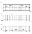
- (A) is a power supply voltage waveform of an AC power supply
- (b) is a waveform of a drive pulse signal generated by a control circuit
- (c) is a diagram showing a change in input current. It is a figure which shows the production
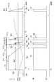
- FIG. 1 is a diagram for explaining a circuit configuration of a power supply device 10 for controlling a compressor of an air conditioner according to the present embodiment.
- the power supply device 10 includes a reactor (inductive element) 12 connected in series to an AC power supply 11, and diode bridges 13a to 13d connected to the AC power supply 11 and the reactor 12.
- Rectifier circuit (rectifier means) 13 smoothing circuit (smoothing means) 14 composed of capacitor 14 a connected in parallel with rectifier circuit 13, and load 15 connected to smoother circuit 14. Yes.
- the power supply device 10 includes a switching member (switch means) 16 that short-circuits the AC power supply 11 via the reactor 12 and a control circuit (control means) 20 that includes a microcomputer or the like that controls the switching of the switching member 16. It has more.
- the power supply device 10 includes a zero cross detection unit (zero cross detection means) 21 that detects the zero cross point of the AC power supply 11 by detecting the voltage of the AC power supply 11 at both ends of the AC power supply 11, and the upstream side of the reactor 12.
- a load current detection unit 22 that detects a current supplied to the load 15 and a load voltage detection unit 23 that detects a DC voltage supplied to the load 15 on the upstream side of the load 15.
- the control circuit 20 synchronizes with the change (sine wave) of the power supply voltage of the AC power supply 11 based on the detection results in the zero cross detection unit 21, the load current detection unit 22, and the load voltage detection unit 23. Control discontinuity.
- the control circuit 20 generates a drive signal for driving the switching member 16 in synchronization with the zero-cross point detected by the zero-cross detection unit 21, and transmits this drive signal to a drive circuit (not shown) of the switching member 16. Then, the switching member 16 is interrupted.
- Such an operation is realized by the control circuit 20 performing a predetermined operation based on a program and a set value stored in the control circuit 20 in advance.
- the diode bridges 13a and 13d act through the reactor 12 and the rectifier circuit 13 as in the case of the conventional DC power supply device described above.
- the charging current of the capacitor 14a flows.
- a voltage charged in the capacitor 14a is applied to the load 15.
- FIG. 2 shows the operation waveforms of the respective parts at this time.
- 2A shows the half cycle of the power supply voltage waveform of the AC power supply
- FIG. 2B shows the waveform of the drive pulse signal generated by the control circuit
- FIG. 2C shows the change in the input current.
- the control circuit 20 generates and outputs a drive pulse signal as shown in FIG. 2B, and details thereof will be described below.
- a reference waveform signal S10 as shown in FIG. 3 is generated in synchronization with the zero cross point detected by the zero cross detector 21.
- the reference waveform signal S10 includes a trapezoidal wave S11a, a first sawtooth wave (triangular wave) S11b, a second sawtooth wave (triangular wave) S11c, and a third sawtooth wave (triangular wave) S11d.
- the drive pulse signal S40 is output by comparing the level signal S20 and the second reference level signal S30.
- the first reference level signal S20 has a constant level, and the first reference level (reference level) Vth1 of the first reference level signal S20 is calculated by the following equation.
- Vth1 trapezoidal wave amplitude ⁇ M ⁇ Sin (T1b / T50 ⁇ 360 °)
- M is a predetermined coefficient indicating the ratio to the amplitude of the trapezoidal wave (for example, 80% of the trapezoidal wave amplitude)
- the second reference level signal S30 is set to a level higher than the first reference level signal S20, and the second reference level (reference level) Vth2 is calculated by the following equation.
- Vth2 sawtooth amplitude ⁇ M ⁇ Sin ((T1b + (T2a + T2b)) / T50 ⁇ 360 °)
- the first reference level signal S20 and the second reference level signal S30 are determined by the time widths T1b, T2a, and T2b as shown in the above equation.
- preset reference values are used for these time widths T2a and T2b.
- the time widths T2a and T2b are preferably set to be twice or more of the maximum order of harmonic measurement (for example, 40th order ⁇ 50 Hz).
- the time width T1b is stored in advance based on the current value supplied to the load 15 detected by the load current detection unit 22 after the power supply device 10 is started, and a preset reference value is used.
- the first reference level Vth1 and the second reference level Vth2 are calculated using the time width T1 and time T3 read from this table.
- a drive pulse signal S40 is generated by comparing S11c and the third sawtooth wave S11d.
- the widths are set to Wa1, Wb1, Wc1, and Wd1.
- the pulse widths when the trapezoidal wave S11a, the first sawtooth wave S11b, the second sawtooth wave S11c, the third sawtooth wave S11d, and the sine wave X are compared are set to Wa2, Wb2, Wc2, and Wd2.
- the pulse width errors of the first pulse P1, the second pulse P2, the third pulse P3, and the fourth pulse P4 are (Wa1-Wa2), (Wb1-Wb2), (Wc1-Wc2), (Wd1-Wd2).
- the second reference level Vth2 is set as described above.
- the control circuit 20 by outputting the drive pulse signal S40 generated in this way, the input current to the load 15 becomes approximate to a sine wave as shown in FIG. It can be effectively reduced.
- the drive pulse signal S40 is converted into the trapezoidal wave S11a, the first sawtooth wave S11b, the second sawtooth wave S11c, and the third sawtooth wave S11d that constitute the reference waveform signal S10, and the first reference level Vth1. And is generated by comparing with the second reference level Vth2.
- the calculation load on the control circuit 20 can be reduced by comparing the reference waveform signal S10 with the first reference level Vth1 and the second reference level Vth2 having a constant level instead of the sine wave.
- the calculation load in the control circuit 20 can be reduced.
- the second pulse P2 and the third pulse P3 having a short short circuit time are output after the first pulse P1 having a short short circuit time.
- the fourth pulse P4 having a short short circuit time is output.
- the fourth pulse P4 in the second half period can contribute to approximating the waveform of the input current to the load 15 to a sine wave.
- the timing of the third sawtooth wave S11d for generating the fourth pulse P4 is controlled by a time T3 that is independent of the other trapezoidal wave S11a, the first sawtooth wave S11b, and the second sawtooth wave S11c.
- the preferable range of the time T3 for generating the fourth pulse P4 is 0.8T ⁇ T3 ⁇ 0.9T, more preferably 0.85T ⁇ T3 ⁇ where T is the half cycle of the power supply voltage fluctuation. 0.9T.
- the harmonic reduction effect can be increased by the third pulse P3.
- the interval between the second pulse P2 and the third pulse P3 not only can the harmonic reduction effect be maximized, but also the harmonic reduction effect is slightly reduced, but the electromagnetic noise of the reactor by multi-pulse control is suppressed. It is also possible to select. (If necessary, the balance between the harmonic reduction effect and the reactor electromagnetic noise suppression effect can be adjusted by setting the time width T2b)
- the power supply device 10 of the present embodiment it is possible to effectively reduce the harmonic components included in the input current while reducing the processing load on the control circuit 20.
- the first reference level Vth1 is set to a level lower than the second reference level Vth2, so that the pulse width of the first pulse P1 is widened to ensure a long short-circuit time.
- the configuration described in the above embodiment can be selected or changed to another configuration as appropriate.
- SYMBOLS 10 Power supply device, 11 ... AC power supply, 12 ... Reactor (inductive element), 13 ... Rectifier circuit (rectifier means), 13a-13d ... Diode bridge, 14 ... Smoothing circuit (smoothing means), 14a ... Capacitor, 15 ... Load ... 16 ... switching member (switch means), 20 ... control circuit (control means), 21 ... zero cross detector (zero cross detector), 22 ... load current detector, 23 ... load voltage detector, P1 ... first pulse (Long pulse), P2 ... second pulse (short pulse), P3 ... third pulse (short pulse), P4 ... fourth pulse (short pulse), S10 ... reference waveform signal, S11a ...
Landscapes
- Engineering & Computer Science (AREA)
- Power Engineering (AREA)
- Physics & Mathematics (AREA)
- Electromagnetism (AREA)
- Rectifiers (AREA)
Abstract
入力電流に含まれる高調波成分をより一層低減することのできる電源装置を提供することを課題とする。 電源装置の制御回路において、互いにレベルが異なる第一基準レベルVth1、第二基準レベルVth2を用いてパルス生成を行い、第一パルスP1と、第二パルスP2、第三パルスP3、第四パルスP4とで、短絡時間を互いに異ならせて設定する。例えば、第一基準レベルVth1を第二基準レベルVth2よりも低いレベルに設定することで、第一パルスP1のパルス幅を広げて短絡時間を長く確保し、高調波を有効に低減する。
Description
本発明は、交流を直流に変換する電源装置に関する。
空気調和機を構成する圧縮機は、コンバータを用いて制御されている。ここで、コンバータへの入力電流に含まれる高調波成分は低減するのが望ましく、このためにこれまでも様々な手法が提案されている(例えば特許文献1)。
また、交流電源からの交流電圧が0Vになった(以下、これをゼロクロスと称することがある)後、交流電源を一定時間短絡させた後に間欠短絡に切り替え、さらに設定時間経過後、次のゼロクロスまで、交流電源の短絡を開放状態とする構成が提案されている。
また、交流電源からの交流電圧変動の半周期ごとにおけるスイッチング手段の短絡回数を、負荷またはインバータの周波数に応じて変更し、高力率・高昇圧能力を実現する構成も提案されている。
交流電圧変動の半周期毎に、交流電源を短絡するパルス信号のパルス幅を、リアクトルに流れる電流の変化が小さくなるように徐々に変化させる構成も提案されている。
交流電圧変動の半周期毎に、交流電源を短絡するスイッチング手段を、所定の周期で、複数回スイッチングさせる構成も提案されている。
交流電源の交流電圧または交流電流の変動のゼロクロスから、所定の遅延時間経過後に高調波低減用パルスを印加することで、力率の向上を図る構成が開示されている。
しかしながら、上記のような様々な手法が提案されていながらも、常に、より一層、高調波成分を低減して力率を向上できる改良が望まれている。また、高調波成分を低減するために、制御回路への負荷の大きな演算を行わなければならない手法もあり、この点を併せて考慮して改良を図る必要がある。
本発明は、このような技術的課題に基づいてなされたもので、入力電流に含まれる高調波成分をより一層低減することのできる電源装置を提供することを目的とする。
本発明は、このような技術的課題に基づいてなされたもので、入力電流に含まれる高調波成分をより一層低減することのできる電源装置を提供することを目的とする。
かかる目的のもと、本発明の電源装置は、交流電源より入力された交流電力を直流電力に変換して負荷に供給する整流手段と、交流電源入力端子と整流手段との間に直列に接続された誘導性素子と、誘導性素子を介して整流手段に加えられる交流電圧経路間に並列に接続され、開閉動作をするスイッチ手段と、整流手段に並列に整流手段の直流端子側に接続された平滑手段と、交流電源から出力される交流電圧波形のゼロクロス点を検出するゼロクロス検出手段と、スイッチ手段の開閉動作を制御する制御手段と、を備える。そして、制御手段は、スイッチ手段を所定の周期で複数回の開閉動作を行わせるため、予め定めた基準波形信号と基準レベルとを比較することで駆動パルス信号を生成する。駆動パルス信号は、スイッチ手段の開時間の長い長パルスと、長パルスに比較して開時間の短い短パルスとを有し、長パルスは、基準波形信号と第一基準レベルとを比較することで生成され、短パルスは、基準波形信号と、第一基準レベルとはレベルが異なる第二基準レベルとを比較することで生成されていることを特徴とする。
このような電源装置によれば、長パルスと短パルスとで、互いに異なるレベルを有する第一基準レベル、第二基準レベルとの比較によりパルスを生成することで、パルス幅を容易に異ならせることができる。
例えば、制御手段において、第一基準レベルまたは第二基準レベルを基準波形信号が上回るときに、スイッチ手段を開とするパルスを駆動パルス信号において生成する場合、第一基準レベルは、第二基準レベルよりも低いレベルを有するものとすれば、例え同一の波形に対してでも、第一基準レベルとの比較により生成されるパルスを、第二基準レベルとの比較により生成されるパルスよりもパルス幅を大きく確保できる。
ここで、長パルスは、基準波形信号に含まれる台形波と第一基準レベルとを比較することで生成し、短パルスは、基準波形信号に含まれる三角波と、第一基準レベルとはレベルが異なる第二基準レベルとを比較することで生成するのが好ましい。これにより、長パルスと短パルスのパルス幅の差を大きく確保できる。
駆動パルス信号は、ゼロクロス点から開始する交流電圧波形の半波長の前半期間内に、長パルスからなる第一パルスと、短パルスからなる第二パルスおよび第三パルスと、を有し、交流電圧波形の半波長の後半期間内に短パルスからなる第四パルスを有するものとすることができる。
ここで、基準波形信号において、第一パルスを生成するための台形波は、ON状態を時間幅T1維持した後、時間幅T1の立ち下がり時間を有するものとするのが好ましい。
また、基準波形信号において、第二パルス、第三パルス、第四パルスを生成するための三角波は、同一の時間幅T2を有するものとするのが好ましい。
第三パルスは、第二パルスに対し、当該第二パルスを生成するための三角波の時間幅T2と同一の時間幅T2だけ遅延するものとするのが好ましい。
第四パルスは、交流電圧波形の半波長をTとしたときに、ゼロクロス点からの時間T3が0.8T≦T3≦0.9Tとなるタイミングで立ち上がるものとするのが好ましい。
ここで、基準波形信号において、第一パルスを生成するための台形波は、ON状態を時間幅T1維持した後、時間幅T1の立ち下がり時間を有するものとするのが好ましい。
また、基準波形信号において、第二パルス、第三パルス、第四パルスを生成するための三角波は、同一の時間幅T2を有するものとするのが好ましい。
第三パルスは、第二パルスに対し、当該第二パルスを生成するための三角波の時間幅T2と同一の時間幅T2だけ遅延するものとするのが好ましい。
第四パルスは、交流電圧波形の半波長をTとしたときに、ゼロクロス点からの時間T3が0.8T≦T3≦0.9Tとなるタイミングで立ち上がるものとするのが好ましい。
さて、本発明の構成によれば、第一基準レベル、第二基準レベルのレベルを変更すれば、長パルスと短パルスの位相をずらすことなく、長パルス、短パルスのパルス幅を変えることができる。
なおここで、第一基準レベル、第二基準レベルは、固定のままとすることもできるが、電源装置の作動中に、これら第一基準レベル、第二基準レベルを変動させることもできる。
また、負荷に供給される負荷電流を検出する負荷電流検出部をさらに備え、制御手段は、負荷電流検出部で検出された負荷電流の大きさに応じ、第一パルス、第二パルス、第三パルス、第四パルスのパルス幅と、第二パルスの第一パルスに対する遅延時間と、第四パルスのゼロクロス点からの遅延時間とのうち、少なくとも一つを変動させるのが好ましい。
このとき、制御手段は、負荷電流検出部で検出された負荷電流の大きさと、第一パルス、第二パルス、第三パルス、第四パルスのパルス幅、第二パルスの第一パルスに対する遅延時間、第四パルスのゼロクロス点からの遅延時間の設定値のうちの少なくとも一つと、を関連付けた情報を予め記憶しているのが好ましい。これにより制御手段における演算負荷が軽減される。
本発明によれば、スイッチ手段を所定の周期で複数回の開閉動作を行わせるための駆動パルス信号を、スイッチ手段の開時間の長い長パルスと、開時間の短い短パルスとを有するものとし、長パルスは、基準波形信号と第一基準レベルとを比較することで生成し、短パルスは、基準波形信号と、第一基準レベルとはレベルが異なる第二基準レベルとを比較することで生成するものとした。このように、長パルスと短パルスとで、互いに異なるレベルを有する第一基準レベル、第二基準レベルとの比較によりパルスを生成することで、パルス幅を容易に異ならせることができる。これにより、入力電流に含まれる高調波成分を、より有効に低減することが可能となり、力率を向上させることができる。また、基準波形信号と、一定レベルを有した第一基準レベル、第二基準レベルとの比較であるため、駆動パルス信号生成のための演算処理も低負荷なものとなる。
以下、添付図面に示す実施の形態に基づいてこの発明を詳細に説明する。
図1は、本実施の形態における空気調和機の圧縮機を制御するための電源装置10の回路構成を説明するための図である。
この図1に示すように、電源装置10は、交流電源11に直列に接続されたリアクタ(誘導性素子)12と、交流電源11とリアクタ12とに接続されたダイオードブリッジ13a~13dにより構成された整流回路(整流手段)13、整流回路13と並列に接続されたコンデンサ14aで構成された平滑回路(平滑手段)14と、平滑回路14に接続された負荷15と、を備えて構成されている。
図1は、本実施の形態における空気調和機の圧縮機を制御するための電源装置10の回路構成を説明するための図である。
この図1に示すように、電源装置10は、交流電源11に直列に接続されたリアクタ(誘導性素子)12と、交流電源11とリアクタ12とに接続されたダイオードブリッジ13a~13dにより構成された整流回路(整流手段)13、整流回路13と並列に接続されたコンデンサ14aで構成された平滑回路(平滑手段)14と、平滑回路14に接続された負荷15と、を備えて構成されている。
また、電源装置10は、交流電源11をリアクタ12を介して短絡させるスイッチング部材(スイッチ手段)16と、スイッチング部材16の断続を制御する、マイコン等からなる制御回路(制御手段)20と、をさらに備えている。
そして、電源装置10は、交流電源11の両端には、交流電源11の電圧を検出することで交流電源11のゼロクロス点を検出するゼロクロス検出部(ゼロクロス検出手段)21と、リアクタ12の上流側において、負荷15に供給される電流を検出する負荷電流検出部22と、負荷15の上流側で、負荷15に供給される直流電圧を検出する負荷電圧検出部23と、を備える。
そして、電源装置10は、交流電源11の両端には、交流電源11の電圧を検出することで交流電源11のゼロクロス点を検出するゼロクロス検出部(ゼロクロス検出手段)21と、リアクタ12の上流側において、負荷15に供給される電流を検出する負荷電流検出部22と、負荷15の上流側で、負荷15に供給される直流電圧を検出する負荷電圧検出部23と、を備える。
制御回路20は、これらゼロクロス検出部21、負荷電流検出部22、負荷電圧検出部23における検出結果に基づいて、交流電源11の電源電圧の変化(正弦波)に同期して、スイッチング部材16の断続を制御する。制御回路20は、ゼロクロス検出部21で検出されたゼロクロス点に同期させて、スイッチング部材16を駆動する駆動信号を生成し、この駆動信号をスイッチング部材16の駆動回路(図示略)に伝達することで、スイッチング部材16を断続させる。このような動作は、制御回路20に予め記憶されたプログラムと設定値とに基づき、制御回路20が所定の動作を行うことで実現される。
次に、電源装置10の動作について説明する。
交流電源11の電源電圧に同期して制御回路20からオン信号が出力されると、スイッチング部材16が閉じ、交流電源11はリアクタ12とダイオードブリッジ13a,13d(または13b,13c)を介して短絡されて電流が流れ始め、この電流は次第に増加する。次に、電源電圧に同期して制御回路20からオフ信号が出力されるとスイッチング部材16は開き、それまでリアクタ12を流れていた短絡電流は整流回路13を介して平滑回路14のコンデンサ14aの充電電流となって減少し始める。その後、交流電源11の電源電圧がピーク電圧付近になると、前述の従来の直流電源装置の場合と同様に、ダイオードブリッジ13a,13d(または13b,13c)の働きによってリアクタ12と整流回路13を介してコンデンサ14aの充電電流が流れる。そして、負荷15には、コンデンサ14aに充電されている電圧が印加されることになる。
交流電源11の電源電圧に同期して制御回路20からオン信号が出力されると、スイッチング部材16が閉じ、交流電源11はリアクタ12とダイオードブリッジ13a,13d(または13b,13c)を介して短絡されて電流が流れ始め、この電流は次第に増加する。次に、電源電圧に同期して制御回路20からオフ信号が出力されるとスイッチング部材16は開き、それまでリアクタ12を流れていた短絡電流は整流回路13を介して平滑回路14のコンデンサ14aの充電電流となって減少し始める。その後、交流電源11の電源電圧がピーク電圧付近になると、前述の従来の直流電源装置の場合と同様に、ダイオードブリッジ13a,13d(または13b,13c)の働きによってリアクタ12と整流回路13を介してコンデンサ14aの充電電流が流れる。そして、負荷15には、コンデンサ14aに充電されている電圧が印加されることになる。
このときの各部の動作波形を図に示したものが図2である。図2(a)は交流電源の電源電圧波形の半周期を示し、(b)は制御回路で発生する駆動パルス信号の波形を示し、(c)は入力電流の変化を示している。
ここで、制御回路20においては、図2(b)に示すような駆動パルス信号を生成して出力するが、その詳細について以下に説明する。
制御回路20においては、ゼロクロス検出部21で検出されたゼロクロス点に同期させて、図3に示すような基準波形信号S10を生成する。この基準波形信号S10は、台形波S11a、第1鋸波(三角波)S11b、第2鋸波(三角波)S11c、第3鋸波(三角波)S11dから構成されている。
台形波S11aは、ゼロクロス検出部21でゼロクロス点が検出されると(このときを時間T0とする)、信号をONし、時間幅T1aだけ遅延させた後、時間幅T1b(=T1a)をかけて信号を立ち下げることで生成される。
第1鋸波S11bは、台形波S11aが立ち下がった時点(=T1a+T1b)で、信号をONとし、時間幅T2aをかけて信号を立ち下げることで生成される。
第2鋸波S11cは、第1鋸波S11bが立ち下がった時点(=T1a+T1b+T2a)から、時間幅T2b(=T2a)だけ遅延した時点(=T1a+T1b+T2a+T2b)で、信号をONとし、時間幅T2c(本実施形態ではT2c=T2a)をかけて信号を立ち下げることで生成される。
第3鋸波S11dは、第2鋸波S11cの後、ゼロクロス点から時間T3だけ経過した時点において信号をONとし、時間幅T2d(本実施形態ではT2d=T2a)をかけて信号を立ち下げることで生成される。
制御回路20では、上記のようにして生成された基準波形信号S10の台形波S11a、第1鋸波S11b、第2鋸波S11c、第3鋸波S11dと、以下のように生成する第一基準レベル信号S20、第二基準レベル信号S30とを比較することで、駆動パルス信号S40を出力する。
第一基準レベル信号S20は、一定のレベルを有しており、第一基準レベル信号S20の第一基準レベル(基準レベル)Vth1は、以下の式により算出される。
Vth1=台形波振幅×M×Sin(T1b/T50×360°)
ここで、Mは、台形波の振幅に対する割合(例えば、台形波振幅の80%)を示す予め定められた係数、T50は、交流電源の周期で、周波数50Hzの交流電源の場合、T50=20msである。
また、第二基準レベル信号S30は、第一基準レベル信号S20よりも高いレベルに設定され、その第二基準レベル(基準レベル)Vth2は、以下の式により算出される。
Vth2=鋸波振幅×M×Sin((T1b+(T2a+T2b))/T50×360°)
ここで、上記の第一基準レベル信号S20、第二基準レベル信号S30は、上式のごとく、時間幅T1b、T2a、T2bによって定まる。これら時間幅T2a、T2bは、予め設定された基準値が用いられる。時間幅T2a、T2bは、高調波測定の最大次数(例えば40次×50Hz)の2倍以上に設定するのが好ましく、例えば、T2a=T2b=1/5kHz=200μsとすることができる。
時間幅T1bは、電源装置10の起動直後は、予め設定された基準値が用いられ、その後は、負荷電流検出部22で検出された、負荷15に供給される電流値に基づき、予め記憶されたテーブルから、電流値に関連付けられた時間幅T1(=T1a=T1b)を読み出して用いられる。また、時間T3についても同様に、予め記憶されたテーブルから、電流値に関連付けられた時間幅T3が読み出される。表1は、そのテーブルの一例を示すものである。
時間幅T1bは、電源装置10の起動直後は、予め設定された基準値が用いられ、その後は、負荷電流検出部22で検出された、負荷15に供給される電流値に基づき、予め記憶されたテーブルから、電流値に関連付けられた時間幅T1(=T1a=T1b)を読み出して用いられる。また、時間T3についても同様に、予め記憶されたテーブルから、電流値に関連付けられた時間幅T3が読み出される。表1は、そのテーブルの一例を示すものである。

このテーブルから読み出した時間幅T1、時間T3を用い、前記の第一基準レベルVth1、第二基準レベルVth2を算出するのである。
制御回路20においては、上記のようにして算出された第一基準レベルVth1、第二基準レベルVth2と、前記の基準波形信号S10を構成する台形波S11a、第1鋸波S11b、第2鋸波S11c、第3鋸波S11dとを比較することで、駆動パルス信号S40を生成する。これには、
台形波S11a > 第一基準レベルVth1 : パルスON
台形波S11a < 第一基準レベルVth1 : パルスOFF
第1鋸波S11b> 第二基準レベルVth2 : パルスON
第1鋸波S11b< 第二基準レベルVth2 : パルスOFF
第2鋸波S11c> 第二基準レベルVth2 : パルスON
第2鋸波S11c< 第二基準レベルVth2 : パルスOFF
第3鋸波S11d> 第二基準レベルVth2 : パルスON
第3鋸波S11d< 第二基準レベルVth2 : パルスOFF
の条件により、パルスのON・OFFを決定する。
このようにして生成された駆動パルス信号S40の例を図2(b)および図3に示す。
ここで、本来は、パルス信号を生成するに際し、正弦波と三角波(鋸波)とを比較するのが一般的である。しかし、時間とともに変化する三角波と正弦波とを比較することでパルス信号を生成すると、制御回路20を構成する処理部(マイコン等)における演算負荷が大きくなる。
そこで、上記のように、第一基準レベルVth1、第二基準レベルVth2と、前記の基準波形信号S10とを比較してパルス信号を生成することで、制御回路20における演算負荷を軽減できる。
ただしこの場合、第一基準レベルVth1、第二基準レベルVth2を用いて処理を行うことで、パルス信号のパルス幅に誤差が生じ得る。ここで、台形波S11aと第一基準レベルVth1により生成される第一パルス(長パルス)P1、第1鋸波S11bと第二基準レベルVth2により生成される第二パルス(短パルス)P2、第2鋸波S11cと第二基準レベルVth2により生成される第三パルス(短パルス)P3、第3鋸波S11dと第二基準レベルVth2により生成される第四パルス(短パルス)P4のそれぞれにおけるパルス幅を、Wa1、Wb1、Wc1、Wd1とする。そして台形波S11a、第1鋸波S11b、第2鋸波S11c、第3鋸波S11dと正弦波Xとを比較した場合のパルス幅を、Wa2、Wb2、Wc2、Wd2とする。すると、第一パルスP1、第二パルスP2、第三パルスP3、第四パルスP4のパルス幅の誤差は、(Wa1―Wa2)、(Wb1―Wb2)、(Wc1―Wc2)、(Wd1―Wd2)、となる。
本実施形態においては、第二パルスP2、第三パルスP3、第四パルスP4を、同じパルス幅として制御するため、第二基準レベルVth2を、前記のごとく、
Vth2=鋸波振幅×M×Sin((T1b+(T2a+T2b))/T50×360°)
としている。
これに対し、例えば、第二パルスP2のみを考えれば、
Vth2=鋸波振幅×M×Sin((T1b+T2a))/T50×360°)
とした方が、精度が向上する。しかし、本実施形態においては、第二パルスP2、第三パルスP3、第四パルスP4を、同じパルス幅(Wb1=Wc1=Wd1)として制御するために第二基準レベルVth2を前式で規定することで、第二パルスP2、第三パルスP3、第四パルスP4の全体において誤差を小さくすることができる。
制御回路20においては、このようにして生成された駆動パルス信号S40を出力することで、負荷15への入力電流は図2(c)のように、正弦波に近似したものとなり、高調波を有効に低減できる。
このとき、制御回路20においては、駆動パルス信号S40を、基準波形信号S10を構成する台形波S11a、第1鋸波S11b、第2鋸波S11c、第3鋸波S11dと、第一基準レベルVth1、第二基準レベルVth2とを比較することで生成する。このように、基準波形信号S10を、正弦波ではなく、一定レベルを有した第一基準レベルVth1、第二基準レベルVth2と比較することで、制御回路20における演算負荷を軽減できる。
また、駆動パルス信号S40のパルス数を常時固定し、第二パルスP2~第四パルスP4を固定幅とすることでも、制御回路20における演算負荷を軽減できる。
このとき、制御回路20においては、駆動パルス信号S40を、基準波形信号S10を構成する台形波S11a、第1鋸波S11b、第2鋸波S11c、第3鋸波S11dと、第一基準レベルVth1、第二基準レベルVth2とを比較することで生成する。このように、基準波形信号S10を、正弦波ではなく、一定レベルを有した第一基準レベルVth1、第二基準レベルVth2と比較することで、制御回路20における演算負荷を軽減できる。
また、駆動パルス信号S40のパルス数を常時固定し、第二パルスP2~第四パルスP4を固定幅とすることでも、制御回路20における演算負荷を軽減できる。
生成された駆動パルス信号S40は、電源電圧の半周期の前半期間において、短絡時間の長い第一パルスP1の後、短絡時間の短い第二パルスP2、第三パルスP3が出力され、後半期間において、短絡時間の短い第四パルスP4が出力される。特に、後半期間の第四パルスP4により、負荷15への入力電流の波形を、正弦波に近似させるのに寄与することができる。この第四パルスP4を発生させるための第3鋸波S11dは、他の台形波S11a、第1鋸波S11b、第2鋸波S11cとは独立した時間T3により、そのタイミングが制御されている。本実施形態においては、第四パルスP4を発生させる好ましい時間T3の範囲は、電源電圧変動の半周期をTとすると、0.8T≦T3≦0.9T、より好ましくは0.85T≦T3≦0.9Tである。
さらに、第三パルスP3により、高調波低減効果を上げることができる。
また、第二パルスP2と第三パルスP3との間隔の調節により、高調波低減効果を最大に得るだけでなく、高調波低減効果は少し低下するが、複数パルス制御によるリアクタの電磁音を抑えるという選択も可能となる。(必要に応じて、高調波低減効果とリアクタ電磁音抑制効果とのバランスを、時間幅T2bの設定により調節可能)
また、第二パルスP2と第三パルスP3との間隔の調節により、高調波低減効果を最大に得るだけでなく、高調波低減効果は少し低下するが、複数パルス制御によるリアクタの電磁音を抑えるという選択も可能となる。(必要に応じて、高調波低減効果とリアクタ電磁音抑制効果とのバランスを、時間幅T2bの設定により調節可能)
上記のようにして、本実施形態の電源装置10によれば、制御回路20における演算処理の負荷を軽減しつつ、入力電流に含まれる高調波成分を有効に低減することが可能となる。
なお、上記実施の形態では、電源装置10の制御回路20における駆動パルス信号S40の生成について説明したが、本発明の主旨を逸脱しない限り、各設定値等は適宜変更することが可能であるのは言うまでもない。
また、第一基準レベルVth1を第二基準レベルVth2よりも低いレベルに設定することで、第一パルスP1のパルス幅を広げて短絡時間を長く確保するようにしたが、他のパルスについても、同様にレベルを異ならせて短絡時間を長く確保したり、短くしたりすることが可能である。さらには、3以上の互いに異なる基準レベルを用いることも可能である。
これ以外にも、本発明の主旨を逸脱しない限り、上記実施の形態で挙げた構成を取捨選択したり、他の構成に適宜変更することが可能である。
また、第一基準レベルVth1を第二基準レベルVth2よりも低いレベルに設定することで、第一パルスP1のパルス幅を広げて短絡時間を長く確保するようにしたが、他のパルスについても、同様にレベルを異ならせて短絡時間を長く確保したり、短くしたりすることが可能である。さらには、3以上の互いに異なる基準レベルを用いることも可能である。
これ以外にも、本発明の主旨を逸脱しない限り、上記実施の形態で挙げた構成を取捨選択したり、他の構成に適宜変更することが可能である。
10…電源装置、11…交流電源、12…リアクタ(誘導性素子)、13…整流回路(整流手段)、13a~13d…ダイオードブリッジ、14…平滑回路(平滑手段)、14a…コンデンサ、15…負荷、16…スイッチング部材(スイッチ手段)、20…制御回路(制御手段)、21…ゼロクロス検出部(ゼロクロス検出手段)、22…負荷電流検出部、23…負荷電圧検出部、P1…第一パルス(長パルス)、P2…第二パルス(短パルス)、P3…第三パルス(短パルス)、P4…第四パルス(短パルス)、S10…基準波形信号、S11a…台形波、S11b、S11c、S11d…鋸波(三角波)、S20…第一基準レベル信号、S30…第二基準レベル信号、S40…駆動パルス信号、T0…時間、T1、T1a、T1b…時間幅、T2、T2a、T2b、T2c、T2d…時間幅、T3…時間、Vth1…第一基準レベル(基準レベル)、Vth2…第二基準レベル(基準レベル)
Claims (11)
- 交流電源より入力された交流電力を直流電力に変換して負荷に供給する整流手段と、
交流電源入力端子と前記整流手段との間に直列に接続された誘導性素子と、
前記誘導性素子を介して前記整流手段に加えられる交流電圧経路間に並列に接続され、開閉動作をするスイッチ手段と、
前記整流手段に並列に前記整流手段の直流端子側に接続された平滑手段と、
前記交流電源から出力される交流電圧波形のゼロクロス点を検出するゼロクロス検出手段と、
前記スイッチ手段の開閉動作を制御する制御手段と、
を備え、
前記制御手段は、前記スイッチ手段を所定の周期で複数回の開閉動作を行わせるため、予め定めた基準波形信号と基準レベルとを比較することで駆動パルス信号を生成し、
前記駆動パルス信号は、前記スイッチ手段の開時間の長い長パルスと、前記長パルスに比較して開時間の短い短パルスとを有し、前記長パルスは、前記基準波形信号と第一基準レベルとを比較することで生成され、前記短パルスは、前記基準波形信号と、前記第一基準レベルとはレベルが異なる第二基準レベルとを比較することで生成されていることを特徴とする電源装置。 - 前記制御手段は、前記第一基準レベルまたは前記第二基準レベルを前記基準波形信号が上回るときに、前記スイッチ手段を開とするパルスを前記駆動パルス信号において生成し、
前記第一基準レベルは、前記第二基準レベルよりも低いレベルを有することを特徴とする請求項1に記載の電源装置。 - 前記長パルスは、前記基準波形信号に含まれる台形波と第一基準レベルとを比較することで生成され、前記短パルスは、前記基準波形信号に含まれる三角波と、前記第一基準レベルとはレベルが異なる第二基準レベルとを比較することで生成されていることを特徴とする請求項1または2に記載の電源装置。
- 前記駆動パルス信号は、前記ゼロクロス点から開始する前記交流電圧波形の半波長の前半期間内に、前記長パルスからなる第一パルスと、前記短パルスからなる第二パルスおよび第三パルスと、を有し、前記交流電圧波形の半波長の後半期間内に前記短パルスからなる第四パルスを有することを特徴とする請求項1から3のいずれか一項に記載の電源装置。
- 前記基準波形信号において、前記第一パルスを生成するための前記台形波は、ON状態を時間幅T1維持した後、時間幅T1の立ち下がり時間を有することを特徴とする請求項4に記載の電源装置。
- 前記基準波形信号において、前記第二パルス、前記第三パルス、前記第四パルスを生成するための前記三角波は、同一の時間幅T2を有していることを特徴とする請求項4または5に記載の電源装置。
- 前記第三パルスは、前記第二パルスに対し、当該第二パルスを生成するための前記三角波の時間幅T2と同一の時間幅T2だけ遅延していることを特徴とする請求項6に記載の電源装置。
- 前記第四パルスは、前記交流電圧波形の半波長をTとしたときに、前記ゼロクロス点からの時間T3が0.8T≦T3≦0.9Tとなるタイミングで立ち上がることを特徴とする請求項4から7のいずれか一項に記載の電源装置。
- 前記負荷に供給される負荷電流を検出する負荷電流検出部をさらに備え、
前記制御手段は、前記負荷電流検出部で検出された前記負荷電流の大きさに応じ、前記第一パルス、前記第二パルス、前記第三パルス、前記第四パルスのパルス幅と、前記第二パルスの前記第一パルスに対する遅延時間と、前記第四パルスの前記ゼロクロス点からの遅延時間とのうち、少なくとも一つを変動させることを特徴とする請求項4から8のいずれか一項に記載の電源装置。 - 前記制御手段は、前記負荷電流検出部で検出された前記負荷電流の大きさと、前記第一パルス、前記第二パルス、前記第三パルス、前記第四パルスのパルス幅、前記第二パルスの前記第一パルスに対する遅延時間、前記第四パルスの前記ゼロクロス点からの遅延時間の設定値のうちの少なくとも一つと、を関連付けた情報を予め記憶していることを特徴とする請求項9に記載の電源装置。
- 前記制御手段は、前記負荷電流検出部で検出された前記負荷電流の大きさに応じ、前記第一基準レベル、前記第二基準レベルを変動させることを特徴とする請求項9または10に記載の電源装置。
Priority Applications (2)
| Application Number | Priority Date | Filing Date | Title |
|---|---|---|---|
| EP10799632.4A EP2456062B1 (en) | 2009-07-14 | 2010-07-14 | Power supply device |
| ES10799632.4T ES2693458T3 (es) | 2009-07-14 | 2010-07-14 | Dispositivo de suministro de potencia |
Applications Claiming Priority (2)
| Application Number | Priority Date | Filing Date | Title |
|---|---|---|---|
| JP2009-165246 | 2009-07-14 | ||
| JP2009165246A JP5409152B2 (ja) | 2009-07-14 | 2009-07-14 | 電源装置 |
Publications (1)
| Publication Number | Publication Date |
|---|---|
| WO2011007568A1 true WO2011007568A1 (ja) | 2011-01-20 |
Family
ID=43449178
Family Applications (1)
| Application Number | Title | Priority Date | Filing Date |
|---|---|---|---|
| PCT/JP2010/004584 WO2011007568A1 (ja) | 2009-07-14 | 2010-07-14 | 電源装置 |
Country Status (4)
| Country | Link |
|---|---|
| EP (1) | EP2456062B1 (ja) |
| JP (1) | JP5409152B2 (ja) |
| ES (1) | ES2693458T3 (ja) |
| WO (1) | WO2011007568A1 (ja) |
Cited By (2)
| Publication number | Priority date | Publication date | Assignee | Title |
|---|---|---|---|---|
| CN103973134A (zh) * | 2013-01-30 | 2014-08-06 | 广东美的制冷设备有限公司 | 直流电源装置及提高其功率因数的pwm脉冲控制方法 |
| WO2014119033A1 (ja) | 2013-01-31 | 2014-08-07 | 三菱重工業株式会社 | コンバータ装置及び空気調和機 |
Families Citing this family (6)
| Publication number | Priority date | Publication date | Assignee | Title |
|---|---|---|---|---|
| JP2013106455A (ja) * | 2011-11-15 | 2013-05-30 | Hitachi Appliances Inc | 直流電源装置およびこれを用いた空気調和機 |
| JP6056425B2 (ja) * | 2012-11-30 | 2017-01-11 | 株式会社ノーリツ | 電源装置 |
| JP6239370B2 (ja) * | 2013-12-20 | 2017-11-29 | 三菱重工業株式会社 | 電源装置及び消費電力推定方法 |
| EP3168974B1 (en) * | 2014-07-08 | 2022-06-15 | Mitsubishi Electric Corporation | Power conversion device |
| US9929637B2 (en) * | 2014-09-26 | 2018-03-27 | Mitsubishi Electric Corporation | Power converting device |
| JP6489689B2 (ja) | 2015-06-17 | 2019-03-27 | 三菱重工サーマルシステムズ株式会社 | ゼロクロス点検出装置、電源装置、ゼロクロス点検出方法及びプログラム |
Citations (5)
| Publication number | Priority date | Publication date | Assignee | Title |
|---|---|---|---|---|
| JPH02299470A (ja) | 1989-05-11 | 1990-12-11 | Fuji Electric Co Ltd | 高力率整流回路 |
| JP2001186770A (ja) * | 1999-12-28 | 2001-07-06 | Mitsubishi Electric Corp | 電源装置およびこれを用いた電動機または圧縮機駆動システム |
| JP2006174689A (ja) * | 2004-11-18 | 2006-06-29 | Matsushita Electric Ind Co Ltd | 直流電源装置 |
| JP2008086073A (ja) * | 2006-09-26 | 2008-04-10 | Daikin Ind Ltd | 電源回路、並びにインバータ、交流モータ、冷媒圧縮機及び空気調和機 |
| JP2008193815A (ja) * | 2007-02-06 | 2008-08-21 | Sharp Corp | 電源装置 |
Family Cites Families (2)
| Publication number | Priority date | Publication date | Assignee | Title |
|---|---|---|---|---|
| US7598714B2 (en) * | 2006-07-12 | 2009-10-06 | Harman International Industries, Incorporated | Amplifier employing interleaved signals for PWM ripple suppression |
| JP5016360B2 (ja) * | 2007-04-12 | 2012-09-05 | 新電元工業株式会社 | スイッチング電源回路、スイッチング電源回路の制御方法および制御プログラム |
-
2009
- 2009-07-14 JP JP2009165246A patent/JP5409152B2/ja active Active
-
2010
- 2010-07-14 ES ES10799632.4T patent/ES2693458T3/es active Active
- 2010-07-14 EP EP10799632.4A patent/EP2456062B1/en active Active
- 2010-07-14 WO PCT/JP2010/004584 patent/WO2011007568A1/ja active Application Filing
Patent Citations (5)
| Publication number | Priority date | Publication date | Assignee | Title |
|---|---|---|---|---|
| JPH02299470A (ja) | 1989-05-11 | 1990-12-11 | Fuji Electric Co Ltd | 高力率整流回路 |
| JP2001186770A (ja) * | 1999-12-28 | 2001-07-06 | Mitsubishi Electric Corp | 電源装置およびこれを用いた電動機または圧縮機駆動システム |
| JP2006174689A (ja) * | 2004-11-18 | 2006-06-29 | Matsushita Electric Ind Co Ltd | 直流電源装置 |
| JP2008086073A (ja) * | 2006-09-26 | 2008-04-10 | Daikin Ind Ltd | 電源回路、並びにインバータ、交流モータ、冷媒圧縮機及び空気調和機 |
| JP2008193815A (ja) * | 2007-02-06 | 2008-08-21 | Sharp Corp | 電源装置 |
Non-Patent Citations (1)
| Title |
|---|
| See also references of EP2456062A4 * |
Cited By (4)
| Publication number | Priority date | Publication date | Assignee | Title |
|---|---|---|---|---|
| CN103973134A (zh) * | 2013-01-30 | 2014-08-06 | 广东美的制冷设备有限公司 | 直流电源装置及提高其功率因数的pwm脉冲控制方法 |
| CN103973134B (zh) * | 2013-01-30 | 2016-09-07 | 广东美的制冷设备有限公司 | 直流电源装置及提高其功率因数的pwm脉冲控制方法 |
| WO2014119033A1 (ja) | 2013-01-31 | 2014-08-07 | 三菱重工業株式会社 | コンバータ装置及び空気調和機 |
| JP2014150622A (ja) * | 2013-01-31 | 2014-08-21 | Mitsubishi Heavy Ind Ltd | コンバータ装置及び空気調和機 |
Also Published As
| Publication number | Publication date |
|---|---|
| ES2693458T3 (es) | 2018-12-11 |
| JP2011024300A (ja) | 2011-02-03 |
| EP2456062A4 (en) | 2014-12-24 |
| EP2456062A1 (en) | 2012-05-23 |
| JP5409152B2 (ja) | 2014-02-05 |
| EP2456062B1 (en) | 2018-10-24 |
Similar Documents
| Publication | Publication Date | Title |
|---|---|---|
| JP5409152B2 (ja) | 電源装置 | |
| JP6225602B2 (ja) | スイッチング電源装置 | |
| US8094473B2 (en) | Bridgeless power factor correction circuit | |
| EP3168974B1 (en) | Power conversion device | |
| JP5272319B2 (ja) | 電力変換装置 | |
| JP5868920B2 (ja) | 電力変換装置 | |
| JP2003530812A (ja) | ピーク検出器を備える安定器 | |
| US20170222572A1 (en) | Power converting apparatus | |
| JP2011152017A (ja) | スイッチング電源装置 | |
| KR20120052759A (ko) | 스위치 모드 전원 공급 장치 및 방법 | |
| WO2015093213A1 (ja) | 電源装置及び消費電力推定方法 | |
| JPH1080139A (ja) | 電源装置 | |
| JP2008193815A (ja) | 電源装置 | |
| JP7151034B2 (ja) | 制御回路、および、dc/dcコンバータ装置 | |
| JP6358861B2 (ja) | 絶縁抵抗測定装置 | |
| JP2002119053A (ja) | スイッチングレギュレータ | |
| JP6505261B2 (ja) | 電力変換装置 | |
| JP6598874B2 (ja) | 電力変換装置 | |
| WO2013024550A1 (ja) | Dc-dcコンバータ、dc-dc変換方法、及び情報機器 | |
| KR101905345B1 (ko) | 전력 변환 장치 | |
| JP7259450B2 (ja) | 三相整流器及び三相整流器の制御方法 | |
| JP4384469B2 (ja) | 直流電源装置 | |
| JP2001178139A (ja) | 単相入力整流装置 | |
| JP2023084791A (ja) | 集積回路および電源回路 | |
| JP2009183040A (ja) | 電力変換装置 |
Legal Events
| Date | Code | Title | Description |
|---|---|---|---|
| 121 | Ep: the epo has been informed by wipo that ep was designated in this application |
Ref document number: 10799632 Country of ref document: EP Kind code of ref document: A1 |
|
| WWE | Wipo information: entry into national phase |
Ref document number: 2010799632 Country of ref document: EP |
|
| NENP | Non-entry into the national phase |
Ref country code: DE |