WO2011001978A1 - 静電吸着構造体及びその製造方法 - Google Patents
静電吸着構造体及びその製造方法 Download PDFInfo
- Publication number
- WO2011001978A1 WO2011001978A1 PCT/JP2010/061059 JP2010061059W WO2011001978A1 WO 2011001978 A1 WO2011001978 A1 WO 2011001978A1 JP 2010061059 W JP2010061059 W JP 2010061059W WO 2011001978 A1 WO2011001978 A1 WO 2011001978A1
- Authority
- WO
- WIPO (PCT)
- Prior art keywords
- sheet members
- electrode
- dielectric
- adsorbed
- electrostatic
- Prior art date
Links
Images


Classifications
-
- H—ELECTRICITY
- H01—ELECTRIC ELEMENTS
- H01L—SEMICONDUCTOR DEVICES NOT COVERED BY CLASS H10
- H01L21/00—Processes or apparatus adapted for the manufacture or treatment of semiconductor or solid state devices or of parts thereof
- H01L21/67—Apparatus specially adapted for handling semiconductor or electric solid state devices during manufacture or treatment thereof; Apparatus specially adapted for handling wafers during manufacture or treatment of semiconductor or electric solid state devices or components ; Apparatus not specifically provided for elsewhere
- H01L21/683—Apparatus specially adapted for handling semiconductor or electric solid state devices during manufacture or treatment thereof; Apparatus specially adapted for handling wafers during manufacture or treatment of semiconductor or electric solid state devices or components ; Apparatus not specifically provided for elsewhere for supporting or gripping
- H01L21/6831—Apparatus specially adapted for handling semiconductor or electric solid state devices during manufacture or treatment thereof; Apparatus specially adapted for handling wafers during manufacture or treatment of semiconductor or electric solid state devices or components ; Apparatus not specifically provided for elsewhere for supporting or gripping using electrostatic chucks
- H01L21/6833—Details of electrostatic chucks
-
- B—PERFORMING OPERATIONS; TRANSPORTING
- B23—MACHINE TOOLS; METAL-WORKING NOT OTHERWISE PROVIDED FOR
- B23Q—DETAILS, COMPONENTS, OR ACCESSORIES FOR MACHINE TOOLS, e.g. ARRANGEMENTS FOR COPYING OR CONTROLLING; MACHINE TOOLS IN GENERAL CHARACTERISED BY THE CONSTRUCTION OF PARTICULAR DETAILS OR COMPONENTS; COMBINATIONS OR ASSOCIATIONS OF METAL-WORKING MACHINES, NOT DIRECTED TO A PARTICULAR RESULT
- B23Q3/00—Devices holding, supporting, or positioning work or tools, of a kind normally removable from the machine
- B23Q3/15—Devices for holding work using magnetic or electric force acting directly on the work
-
- H—ELECTRICITY
- H02—GENERATION; CONVERSION OR DISTRIBUTION OF ELECTRIC POWER
- H02N—ELECTRIC MACHINES NOT OTHERWISE PROVIDED FOR
- H02N13/00—Clutches or holding devices using electrostatic attraction, e.g. using Johnson-Rahbek effect
-
- Y—GENERAL TAGGING OF NEW TECHNOLOGICAL DEVELOPMENTS; GENERAL TAGGING OF CROSS-SECTIONAL TECHNOLOGIES SPANNING OVER SEVERAL SECTIONS OF THE IPC; TECHNICAL SUBJECTS COVERED BY FORMER USPC CROSS-REFERENCE ART COLLECTIONS [XRACs] AND DIGESTS
- Y10—TECHNICAL SUBJECTS COVERED BY FORMER USPC
- Y10T—TECHNICAL SUBJECTS COVERED BY FORMER US CLASSIFICATION
- Y10T29/00—Metal working
- Y10T29/49—Method of mechanical manufacture
- Y10T29/49002—Electrical device making
- Y10T29/49117—Conductor or circuit manufacturing
Definitions
- the present invention relates to an electrostatic attraction structure that electrically adsorbs an object to be adsorbed, and a method for manufacturing the same, and more particularly, forms a solid integrated structure when used and freely changes the configuration of the structure after use.
- the present invention relates to an electrostatic adsorption structure that can be performed, and a method for manufacturing the same.
- the electrostatic adsorption structure that electrically adsorbs and holds objects to be adsorbed is used to adsorb and hold semiconductor substrates and glass substrates, and also used to adsorb and hold sheet materials such as paper and resin. It is used in a wide range of applications. Electrostatic adsorption structure is usually used by adsorbing an object to be adsorbed with the surface of one dielectric as an adsorption surface by sandwiching the electrode from above and below with a dielectric and applying a voltage to the electrode with an adsorption power source. Further, for example, when used in a semiconductor manufacturing process or the like, it is integrally bonded to a metal base provided with a conduit through which a coolant such as a cooling gas flows.
- the Coulomb force type that uses the electrostatic adsorption force generated between the electrode and the object to be adsorbed, or between the dielectric and the object to be adsorbed placed
- a non-uniform electric field is formed by generating a potential difference between two comb-shaped electrodes.
- Gradient force types that use the generated attracting force are known, and there are structures that use these attracting forces individually and structures that use a combination of multiple forces.
- the electrostatic adsorption structure is formed while selecting the type and characteristics of the dielectric as well as making the electrode monopolar or bipolar.
- a ceramic material having a predetermined volume resistivity is used as a dielectric, and the electrode is embedded in the dielectric by hot pressing so as to sandwich the electrode.
- an insulating film is used for the purpose of preventing dust generation.
- an electrode is sandwiched between polyimide films, and thermocompression bonding is performed via an adhesive film or an adhesive.
- the adsorption force is expressed regardless of the material to be adsorbed, and therefore, it is used to adsorb things other than the semiconductor substrate.
- the present inventors have proposed the apparatus suitable for adsorb
- the gradient force usually, a larger adsorption force can be obtained by narrowing the distance between the electrodes.
- the discharge between the electrodes becomes a problem when the distance becomes shorter, a high voltage cannot be applied. Therefore, in the apparatus proposed by the present inventors, two electrodes are arranged one above the other, and an electrostatic adsorption structure having an interelectrode insulating layer (dielectric) interposed between them is used. The reliability of insulation is increased.
- an electrostatic adsorption structure is usually formed by firmly adhering a dielectric and an electrode to form a strong integrated structure for the purpose of uniformly expressing an adsorption force.
- they are firmly bonded to each other for the purpose of ensuring the thermal conductivity to the object to be adsorbed. Therefore, once formed electrostatic adsorption structure, for example, even if the adsorption surface is scratched or partially consumed, it is difficult to partially remove the adsorption surface and replace it. Then, it is necessary to perform a process such as mechanically scraping all the dielectric on the surface and forming a separate dielectric.
- the present inventors have made it possible to more easily obtain an electrostatic adsorption structure in which electrodes are arranged one above the other through a dielectric, and the structure of the structure once formed.
- a plurality of sheet members each having an electrode sandwiched between dielectrics are superposed, and the electrostatic attraction force generated between the electrodes of each sheet member is reduced.
- the object to be adsorbed can be adsorbed while maintaining a strong integrated structure during use, and between these sheet members can be easily removed by removing the voltage application after use.
- the present invention has been completed.
- an object of the present invention is to provide an electrostatic attraction structure that can maintain a strong integrated structure during use and can freely change the structure of the structure after use.
- Another object of the present invention is to obtain an electrostatic adsorption structure in which electrodes are arranged vertically via a dielectric, and can easily and reliably change the structure after use. It is an object of the present invention to provide a method for manufacturing an electrostatic adsorption structure that can be made.
- the present invention is an electrostatic attraction structure that uses an object to be adsorbed by being electrically adsorbed, and includes a plurality of sheet members in which electrodes are sandwiched between two dielectrics, and at least one adsorption power source. And stacking a plurality of sheet members and applying a voltage between the electrodes of the opposing sheet members by an adsorption power source to electrically adsorb and fix between the opposing sheet members, and the surface outermost layer or The sheet member corresponding to the outermost layer on the back surface is used by adsorbing an object to be adsorbed on the dielectric of one or both outermost sheet members, and after use, a plurality of layers are stacked by releasing the application of voltage.
- An electrostatic attraction structure characterized in that the sheet members can be separated from each other.
- the present invention is a method for manufacturing the electrostatic adsorption structure, wherein a plurality of sheet members are stacked while being positioned to each other, and a voltage is applied between the electrodes of the opposing sheet members by an adsorption power source,
- An electrostatic adsorption structure characterized in that a plurality of laminated sheet members can be separated from each other after the application of voltage is released by integrally forming the sheet members opposite to each other and integrally forming them. It is a manufacturing method of a body.
- the electrostatic adsorption structure of the present invention has a plurality of sheet members and at least one adsorption power source, and applies a voltage from the adsorption power source between the electrodes of the opposing sheet members while laminating the plurality of sheet members.
- the sheet members are attracted to each other by the electrostatic attraction force generated between the electrodes of the opposing sheet members, and are integrally formed. That is, the sheet member has an electrode sandwiched between two dielectrics, and when a voltage is applied by an adsorption power source, an electrostatic adsorption force can be developed between the electrodes of the opposed sheet members.
- outermost layer sheet member one or both of the sheet members positioned in the outermost layer on the front side or the back side.
- the body can be used as an adsorption surface to adsorb the object to be adsorbed.
- a plurality of sheet members are preferably used in order to generate an adsorption force that reaches the adsorption surface side between the sheet member and the electrode of the opposite sheet member. It is preferable that an electrode having an opening is provided so that the lines of electric force generated between the electrodes of the opposing sheet member can reach the suction surface side. In order to obtain a larger adsorbing force, it is preferable that the sheet member laminated opposite to the outermost layer sheet member having an electrode having an opening corresponds to at least the electrode opening of the outermost layer sheet member. The electrode should be present at the position.
- the opposing sheet member has an electrode at the projected position.
- both the outermost layer sheet members have electrodes having openings, it is needless to say that they can be used as a double-sided adsorption structure that adsorbs an object to be adsorbed on both sides.
- the electrode having a plurality of openings examples include a mesh electrode having a plurality of openings having a predetermined shape such as a circle, a grid electrode, and a pattern electrode such as a comb-like electrode, The present invention is not limited to these, and the number, size, shape, and the like of the openings can be appropriately designed according to the type and size of the object to be adsorbed.
- the electrode of the sheet member that does not adsorb the object to be adsorbed may be an electrode having a plurality of openings, or may be provided with a planar electrode having no openings.
- the suction power source for applying a voltage between the electrodes of the opposed sheet members the same power source as that used in a general electrostatic suction structure can be used, and light energy is converted into electrical energy.
- one suction power source may be used for each facing sheet member, and one suction power source may be used between all the facing sheet member electrodes. A voltage may be applied.
- a voltage is applied between the electrodes of the opposing sheet members by the adsorption power source so that the opposing sheet members are adsorbed and an adsorption force for the object to be adsorbed is also generated on the adsorption surface side.
- the sheet member may be provided with a bipolar electrode, and a voltage is applied between the electrodes in the sheet member to develop an adsorption force between the opposing sheet members. You may make it express the adsorption power with respect to a to-be-adsorbed object.
- Ceramics are formed by thermal spraying ceramic films such as alumina (Al 2 O 3 ) powder, aluminum nitride (AlN) powder, zirconia (ZrO 2 ) powder, in addition to insulating films such as polyimide and ceramic plates.
- Thermal spray film etc. can be mentioned, but it should be used for exhibition equipment used indoors and outdoors or dust collection equipment that adsorbs dust and dirt in the atmosphere by adsorbing exhibits made of paper or resin sheet.
- plastic films such as polyethylene terephthalate (PET), polyester, acrylic resin, epoxy resin, polyethylene, celluloid, and polyvinyl chloride.
- PET polyethylene terephthalate
- the dielectric may be formed by printing insulating ink.
- the thickness of the dielectric varies depending on the materials used and the purpose of use of the structure. For example, when used for an exhibition apparatus or a dust collector used indoors or outdoors, a PET film or an insulating ink is used. It is preferable to form a structure including a dielectric having a thickness of about 20 to 70 ⁇ m.
- the two dielectrics sandwiching the electrode may be made of different materials, or each dielectric may be formed of a plurality of layers of two or more layers.
- the electrode forming the sheet member is not particularly limited in terms of its material, manufacturing method, etc.
- the metal film formed by metal foil, sputtering method, ion plating method or the like may be obtained by etching into a predetermined shape.
- a predetermined shape may be obtained by spraying a metal material or printing a conductive ink.
- the thickness of the electrode varies depending on the purpose of use of the structure, but is generally about 5 to 20 ⁇ m.
- the laminated sheet members are electrically adsorbed and fixed to each other by applying a voltage between the electrodes of the respective sheet members by an adsorption power source.
- it may be fixed in advance by a fixing means.
- a fixing means it is possible to maintain a positioned state until a voltage is applied to each electrode of the laminated sheet member, and the application of the voltage is released. Later, it should be easy to separate between the sheet members, so-called temporary fastening means, for example, a double-sided adhesive tape with adhesive applied on both sides. It can be used suitably.
- the electrostatic attraction structure of the present invention can adsorb an object to be adsorbed while maintaining a strong integrated structure at the time of use, and after use, by canceling the application of voltage, a plurality of stacked sheets Since the members can be separated from each other, for example, a part of the laminated sheet member is turned over so that the other dielectric is used as a new attracting surface, the lamination order of the sheet members is changed, or some sheets are It is possible to easily replace only the member with a new one, and furthermore, the number of sheet members to be stacked can be easily increased or decreased. The adsorptive power to be developed can be changed accordingly.
- the electrostatic adsorption structure of the present invention in use, a strong integrated structure in which electrodes are arranged on both sides of the dielectric is maintained, and the object to be adsorbed is adsorbed using the dielectric of the outermost sheet member as the adsorption surface. Since the sheet members can be easily separated after use, the configuration of the structure itself can be freely changed.
- an electrostatic attraction structure having electrodes arranged vertically through a dielectric can be obtained easily and reliably, and the configuration of the structure itself can be changed. Can be obtained.
- FIG. 1 is a cross-sectional explanatory view for explaining an electrostatic attraction structure adopted as an attraction / holding means in the electrostatic chuck device of Example 1 of the present invention.
- FIG. 2 is an explanatory plan view (A) and (B) of an electrode employed in the electrostatic attraction structure according to Example 1 of the present invention.
- FIG. 3 is a cross-sectional explanatory view for explaining an exhibition / posting apparatus according to Embodiment 2 of the present invention.
- FIG. 4 is an explanatory plan view (A) and (B) of an electrode employed in an electrostatic attraction structure according to Embodiment 2 of the present invention.
- FIG. 5 is an explanatory diagram for explaining an electrostatic attraction structure according to Embodiment 2 of the present invention.
- FIG. 6 is a cross-sectional explanatory view for explaining an electrostatic attraction structure according to Embodiment 3 of the present invention.
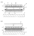
- Example 1 there is an electrostatic chuck device that uses the electrostatic adsorption structure X according to the first embodiment of the present invention as means for adsorbing and holding a semiconductor substrate such as a silicon wafer in a semiconductor manufacturing process such as plasma etching. It is shown.
- the electrostatic chucking structure X as the semiconductor substrate chucking / holding unit includes sheet members 5 and 15 and a chucking power source 4 and is not shown in the figure.
- An electrostatic chuck device is formed integrally with an aluminum base 7 provided with a pipe and the like, and a semiconductor substrate 8 such as a silicon wafer is formed using the dielectric 2 of the sheet member 5 in the electroadsorption structure X as an adsorption surface. Can be adsorbed and held.
- the sheet member 5 is etched so that copper is vapor-deposited on the surface of the dielectric 1 made of a polyimide film having a size of 320 mm long ⁇ 320 mm wide ⁇ 50 ⁇ m thick, and then formed into a predetermined shape.
- An electrode 3 having a length of 300 mm ⁇ width of 300 mm ⁇ thickness of 3 ⁇ m is formed, and a polyimide film is laminated via a bonding sheet (not shown) so as to cover the electrode 3, and the length of 320 mm ⁇ width of 320 mm ⁇ thickness of 50 ⁇ m.
- the dielectric 2 is formed.
- the electrode 3 as a plan view in FIG.
- the other sheet member 15 is formed by depositing copper to form a planar electrode 13 having a length of 300 mm, a width of 300 mm, and a thickness of 3 ⁇ m without an opening.
- the dielectric member 11 is made of a polyimide film and has a thickness of 50 ⁇ m
- the dielectric member 12 is also made of a polyimide film and has a thickness of 50 ⁇ m.
- a double-sided adhesive tape 6 is affixed to the edge of the body 11, and the dielectric 1 side is overlapped and fixed while positioning the remaining sheet member 5.
- a DC power source (adsorption power source) 4 is connected between the electrode 3 of the sheet member 5 and the electrode 13 of the sheet member 15 via a connection terminal and a switch (both not shown). Is +1 kV, and a voltage of ⁇ 1 kV can be applied to the electrode 13.
- the switch of the suction power source 4 constituting the electroadsorption structure X is turned on, and the electrodes 3 and 13 are connected.
- an electrostatic attracting force is generated between the sheet member 5 and the sheet member 15 to be attracted and fixed to each other.
- the dielectric 2 of the sheet member 5 is passed through the opening 3a. Since the lines of electric force generated between the electrode 3 and the electrode 13 reach and an adsorption force is developed, the semiconductor substrate 8 can be adsorbed.
- the semiconductor substrate 8 is made dielectric by opening the switch of the adsorption power source 4 and releasing the application of voltage. While being able to remove from the body 2, since the electrostatic attraction force which generate
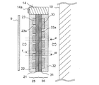
- Example 2] 3 to 5 show an exhibition / posting apparatus that uses the electrostatic adsorption structure X according to the second embodiment of the present invention as display means for display / posting.
- the electrostatic adsorption structure X as the display means includes sheet members 25 and 35 and an adsorption power source 14, and the dielectric member 32 side of the sheet member 35 is, for example, the wall surface 10.
- the posting 9 made of a sheet of paper or resin can be adsorbed on the dielectric 22 side of the sheet member 25.
- the sheet member 25 is obtained by screen-printing carbon ink (JELCON model CH-10 manufactured by Jujo Chemical Co., Ltd.) on a PET film (dielectric) 21 having a size of 400 mm long ⁇ 600 mm wide ⁇ 50 ⁇ m thick.
- An electrode 23 having a length of 350 mm, a width of 550 mm, and a thickness of 10 ⁇ m is formed, and an insulating ink (JELCON model AC-3G manufactured by Jujo Chemical Co., Ltd.) is screen-printed so as to cover the electrode 23, and the length is 400 mm ⁇ width 600 mm ⁇ thickness. It is obtained by forming a dielectric 22 having a thickness of 50 ⁇ m.
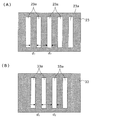
- the electrodes 23 as plan view in FIG.
- electrode width d 1 is 3 mm
- the opening width d 2 is formed with a plurality of openings 23a of 1 mm.
- the other sheet member 35, as a plan view in FIG. 4 (B) are shown, electrode width d 1 of the electrode 33 is 3 mm, while allowing the opening width d 2 has a plurality of openings 33a of 1 mm, the opening It is formed in the same manner as the sheet member 25 except that the position of the portion 33a is different from the pattern of the electrode 23.
- the adsorption power source 14 includes a solar cell 14a and a booster circuit 14b that boosts the power generated by the solar cell 14a, and stores the power generated by the solar cell 14a.
- a large-capacitance capacitor 14c having an energy capacity of 200 mWh is provided so that a voltage can be applied to the electrode 23 and the electrode 33 even when the power generation capacity of the solar cell 14a is temporarily stopped or decreased.
- the booster circuit 14b is provided with a power switch 14d for turning on and off the application of voltage to the electrodes 23 and 33.
- the sheet members 25 and 35 constituting the electrostatic adsorption structure X and the adsorption power source 14 are integrally formed. It is only necessary to connect the electrodes 23 and 33 so that a voltage is applied, and these are connected by a relatively long connection cable, and the adsorption power source 14 is installed in a place convenient for power generation by the solar cell 14a. You may make it do.
- the PET film 21 of the sheet member 25 and the PET film 31 of the sheet member 35 are overlapped and positioned while being fixed with, for example, a double-sided adhesive tape (not shown).
- the sheet member 35 is positioned so that the electrode exists at a position corresponding to the opening 23 a of the electrode 23 that forms the sheet member 25, and the sheet member 25 is positioned on the electrode 33 that forms the sheet member 35.
- Positioning is performed so that the electrode exists at a position corresponding to the opening 33a. That is, as shown in FIG.
- the electrodes 23 and 33 both have a gap of 1 mm in width, and the PET of the opposing sheet member
- the other electrode is formed so as to block the portion corresponding to the gap between the one electrode through the films 21 and 31, and the opening 23a in the electrode 23 of the sheet member 25 is formed as shown by an arrow i in FIG.
- the electrode 33 of the sheet member 35 exists, and as indicated by the arrow ii, the opening 33a of the electrode 33 of the sheet member 35 is projected at the position projected in the thickness direction.
- the member 25 is positioned so that the electrode 23 exists. As indicated by an arrow iii, the overlapping portion in the thickness direction of the electrode 23 and the electrode 33 is 1 mm at both ends.
- the dielectric member 32 side of the overlapped sheet member 25 and sheet member 35 is positioned on the predetermined wall surface 10 with the power switch 14d turned off.
- the power switch 14d is turned on, and a voltage is applied between the electrodes 23 and 33 to electrically adsorb and fix the sheet member 25 and the sheet member 35.
- the body X is adsorbed and fixed, and the posting material 9 is attached to the surface of the dielectric 22 of the sheet member 25 for posting.
- the power switch 14d is turned off and the posting 9 is once removed.
- the electrostatic adsorption structure X is removed from the wall surface 10, for example, the electrostatic adsorption structure X is turned over, and the dielectric member 22 side of the sheet member 25 faces the wall surface 10, and is posted on the dielectric 32 of the sheet member 35. 9 may be used by pasting.
- the electrostatic adsorbing structure X is formed by making the dielectric 22 of the sheet member 25 and the PET film 31 of the sheet member 35 face each other so that only the sheet member 25 is turned over and the PET film 21 side becomes the adsorption surface of the posting. You may make it form.
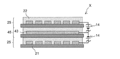
- the electrostatic chuck structure X according to the third embodiment uses two sheet members 25 on which the electrostatic chuck structure X according to the second embodiment is formed, and further includes a sheet member 45 interposed therebetween. Thus, three sheet members are laminated. Among these, the sheet member 45 is the same as the sheet member 25 except that the opening 43 is not provided and the electrode 43 having a length of 350 mm ⁇ width of 550 mm ⁇ thickness of 10 ⁇ m is provided so that the entire surface becomes an electrode. Is formed. Further, in the electrostatic chucking structure X according to the third embodiment, the same as in the second embodiment except that two suction power sources 14 are used and a voltage is applied between the electrodes of the facing sheet members. It is formed.
- the suction force generated between the facing sheet members can be increased as compared with the second embodiment.
- the electrostatic chuck structure The body X itself can be made larger to adsorb larger postings, etc., or can be used in various ways by changing the purpose of use or the purpose of use.
- the electrostatic adsorption structure X of the present invention described in the first to third embodiments can be used for applications other than the apparatuses described in the respective embodiments. In addition to other applications in the field, etc., it can be used as an air cleaning device that collects dust and dust in the air, sterilizes and sterilizes viruses and pathogenic bacteria, etc.
- the present invention can also be used for a device that collects metal in liquid by using it in water or liquid, or a chip removal device that removes cutting waste generated at various work sites.
Abstract
Description
図1及び図2において、本発明の実施例1に係る静電吸着構造体Xをプラズマエッチング等の半導体製造プロセスでシリコンウエハ等の半導体基板を吸着・保持する手段として利用する静電チャック装置が示されている。
この実施例1の静電チャック装置において、上記半導体基板の吸着・保持手段としての静電吸着構造体Xは、シート部材5及び15と吸着電源4とを有し、冷却媒体を流す図示外の管路等を備えたアルミ製ベース7と一体に形成されて静電チャック装置を構成し、電吸着構造体Xにおけるシート部材5の誘電体2を吸着面として、シリコンウエハ等の半導体基板8を吸着・保持することができる。
図3~図5において、本発明の実施例2に係る静電吸着構造体Xを展示・掲示用の表示手段として利用する展示・掲示装置が示されている。
この実施例2の展示・掲示装置において、上記表示手段としての静電吸着構造体Xは、シート部材25及び35と吸着電源14とを有し、シート部材35の誘電体32側を例えば壁面10に吸着させ、シート部材25の誘電体22側に紙や樹脂製のシートからなる掲示物9を吸着させることができる。
図6において、上記実施例2で利用した静電吸着構造体Xの変形例が示されている。この実施例3に係る静電吸着構造体Xは、実施例2における静電吸着構造体Xを形成したシート部材25を2枚利用し、更にこれらの間に、シート部材45を介装するようにして、3枚のシート部材を積層して形成される。このうちシート部材45は、開口部を形成せずに、全面が電極となるようにした縦350mm×横550mm×厚さ10μmの電極43を備えるようにした以外は、シート部材25と同様にして形成されている。また、この実施例3に係る静電吸着構造体Xでは、吸着電源14を2つ使用して、対向したシート部材の電極間に電圧を印加するようにした以外は実施例2と同様にして形成される。
3,13,23,33,43:電極
3a,23a,33a:開口部
4,14:吸着電源
14a:太陽電池
14b:昇圧回路
14c:大容量コンデンサー
14d:電源スイッチ
5,15,25,35,45:シート部材
6:両面粘着テープ
7:金属製ベース
8:半導体基板
9:掲示物
10:壁面
X:静電吸着構造体
Claims (7)
- 被吸着物を電気的に吸着して使用する静電吸着構造体であって、
2つの誘電体の間に電極が挟み込まれた複数のシート部材と、少なくとも1つの吸着電源とを有し、複数のシート部材を積層して、吸着電源によって対向するシート部材の電極間に電圧を印加することで、対向するシート部材間を電気的に吸着固定させると共に、表面最外層又は裏面最外層にあたるシート部材のうち、いずれか一方又は両方の最外層シート部材の誘電体に被吸着物を吸着させて使用し、使用後には、電圧の印加を解除することで、積層された複数のシート部材間が互いに分離可能になるようにしたことを特徴とする静電吸着構造体。 - 最外層シート部材のいずれか一方又は両方が、複数の開口部を有した電極を備えており、開口部を有した電極を持つ最外層シート部材に対向して積層されるシート部材は、少なくとも開口部に対応する位置に電極が存在するようにしたことを特徴とする請求項1に記載の静電吸着構造体。
- 複数のシート部材が互いに位置決めされた状態で、固定手段によって固定されている請求項1又は2に記載の静電吸着構造体。
- 絶縁性フィルムに導電性インクを印刷して所定の電極を形成し、この電極を覆うように絶縁性インクを印刷することによって得られたシート部材を複数積層してなる請求項1又は2に記載の静電吸着構造体。
- 絶縁性フィルムからなる誘電体に導電性インクを印刷して複数の開口部を有した電極を形成し、この電極を覆うように絶縁性インクを印刷して誘電体を形成した2枚のシート部材を重ね合わせ、表裏面両方の誘電体に被吸着物を吸着させて使用することができる請求項4に記載の静電吸着構造体。
- 絶縁性フィルムからなる誘電体の厚さが20~70μmであり、絶縁性インクからなる誘電体の膜厚が20~70μmであり、導電性インクからなる電極の膜厚が5~20μmである請求項5に記載の静電吸着構造体。
- 請求項1~6のいずれかに記載の静電吸着構造体を製造する方法であって、
複数のシート部材を互いに位置決めしながら積層し、吸着電源によって対向するシート部材の電極間に電圧を印加することで、対向するシート部材間を電気的に吸着固定させて一体に形成し、電圧の印加を解除した後には、積層した複数のシート部材間を互いに分離できるようにすることを特徴とする静電吸着構造体の製造方法。
Priority Applications (7)
| Application Number | Priority Date | Filing Date | Title |
|---|---|---|---|
| US13/381,868 US20120120545A1 (en) | 2009-07-02 | 2010-06-29 | Electrostatic attracting structure and fabricating method therefor |
| EP10794147.8A EP2450948B1 (en) | 2009-07-02 | 2010-06-29 | Electrostatic attracting structure and fabricating method therefor |
| SG2011097516A SG177448A1 (en) | 2009-07-02 | 2010-06-29 | Electrostatic attracting structure and fabricating method therefor |
| KR1020177001490A KR101806926B1 (ko) | 2009-07-02 | 2010-06-29 | 양면 흡착 구조체, 양면 흡착 구조체의 제조방법, 및 양면 흡착 구조체를 이용한 피흡착물의 흡착방법 |
| JP2011520931A JP5500172B2 (ja) | 2009-07-02 | 2010-06-29 | 静電吸着構造体及びその製造方法 |
| CN201080028921.9A CN102473668B (zh) | 2009-07-02 | 2010-06-29 | 静电吸附构造体及其制造方法 |
| HK12108910.6A HK1168200A1 (en) | 2009-07-02 | 2012-09-12 | Electrostatic attracting structure and fabricating method therefor |
Applications Claiming Priority (2)
| Application Number | Priority Date | Filing Date | Title |
|---|---|---|---|
| JP2009-157460 | 2009-07-02 | ||
| JP2009157460 | 2009-07-02 |
Publications (1)
| Publication Number | Publication Date |
|---|---|
| WO2011001978A1 true WO2011001978A1 (ja) | 2011-01-06 |
Family
ID=43411050
Family Applications (1)
| Application Number | Title | Priority Date | Filing Date |
|---|---|---|---|
| PCT/JP2010/061059 WO2011001978A1 (ja) | 2009-07-02 | 2010-06-29 | 静電吸着構造体及びその製造方法 |
Country Status (9)
| Country | Link |
|---|---|
| US (1) | US20120120545A1 (ja) |
| EP (1) | EP2450948B1 (ja) |
| JP (1) | JP5500172B2 (ja) |
| KR (2) | KR101806926B1 (ja) |
| CN (1) | CN102473668B (ja) |
| HK (1) | HK1168200A1 (ja) |
| SG (1) | SG177448A1 (ja) |
| TW (1) | TW201130081A (ja) |
| WO (1) | WO2011001978A1 (ja) |
Cited By (9)
| Publication number | Priority date | Publication date | Assignee | Title |
|---|---|---|---|---|
| WO2012123188A1 (en) | 2011-03-17 | 2012-09-20 | Asml Netherlands B.V. | Electrostatic clamp, lithographic apparatus, and device manufacturing method |
| WO2015111616A1 (ja) * | 2014-01-22 | 2015-07-30 | 株式会社アルバック | プラズマ処理装置、及びウェハ搬送用トレイ |
| TWI514510B (ja) * | 2013-12-23 | 2015-12-21 | ||
| JP2017506429A (ja) * | 2014-02-05 | 2017-03-02 | マイクロン テクノロジー, インク. | 静電力による半導体ボンディング強化用のデバイス、システムおよび方法 |
| KR20180014068A (ko) * | 2015-06-11 | 2018-02-07 | 프라운호퍼 게젤샤프트 쭈르 푀르데룽 데어 안겐반텐 포르슝 에. 베. | 기판 캐리어로의 기판의 정전기적 커플링을 위한 필름을 갖는 장치 |
| JP6435481B1 (ja) * | 2017-09-04 | 2018-12-12 | 株式会社プロセス・ラボ・ミクロン | ワーク吸着冶具とワーク吸着装置 |
| WO2019188341A1 (ja) | 2018-03-29 | 2019-10-03 | 株式会社クリエイティブテクノロジー | 吸着パッド |
| WO2020027246A1 (ja) | 2018-08-02 | 2020-02-06 | 株式会社クリエイティブテクノロジー | 静電吸着体 |
| CN112313871A (zh) * | 2018-06-28 | 2021-02-02 | 3M创新有限公司 | 低电压静电挤压装置 |
Families Citing this family (5)
| Publication number | Priority date | Publication date | Assignee | Title |
|---|---|---|---|---|
| CN107068592B (zh) * | 2017-02-28 | 2023-07-25 | 广东工业大学 | 一种静电吸附拾取夹具系统 |
| JP6811144B2 (ja) * | 2017-05-30 | 2021-01-13 | 東京エレクトロン株式会社 | プラズマ処理装置の静電チャックを運用する方法 |
| FR3074957A1 (fr) * | 2017-12-08 | 2019-06-14 | Commissariat A L'energie Atomique Et Aux Energies Alternatives | Procede de collage par adhesion directe d'un premier substrat a un deuxieme substrat |
| US11949350B2 (en) | 2018-06-28 | 2024-04-02 | 3M Innovative Properties Company | Flexible devices with jamming components |
| CN110228283B (zh) * | 2019-07-18 | 2020-10-09 | 清华大学 | 基于静电吸附的快速、选择性转印装置及其制造方法 |
Citations (7)
| Publication number | Priority date | Publication date | Assignee | Title |
|---|---|---|---|---|
| JPH02135141U (ja) * | 1989-04-17 | 1990-11-09 | ||
| JPH05198663A (ja) * | 1992-01-21 | 1993-08-06 | Hitachi Ltd | 試料搬送ホルダ |
| JPH0833359A (ja) * | 1994-07-19 | 1996-02-02 | Mitsubishi Chem Corp | 静電アクチュエータの製造方法 |
| JPH11111829A (ja) * | 1997-10-06 | 1999-04-23 | Ulvac Corp | 静電吸着ホットプレート、真空処理装置、及び真空処理方法 |
| JP2003124298A (ja) * | 2001-10-17 | 2003-04-25 | Anelva Corp | プラズマ支援ウェハー処理反応容器の二重静電チャックウェハーステージ |
| WO2005091356A1 (ja) | 2004-03-19 | 2005-09-29 | Creative Technology Corporation | 双極型静電チャック |
| WO2007066572A1 (ja) * | 2005-12-06 | 2007-06-14 | Creative Technology Corporation | 静電チャック用電極シート及び静電チャック |
Family Cites Families (6)
| Publication number | Priority date | Publication date | Assignee | Title |
|---|---|---|---|---|
| JPH01135141U (ja) * | 1988-03-10 | 1989-09-14 | ||
| US5532903A (en) * | 1995-05-03 | 1996-07-02 | International Business Machines Corporation | Membrane electrostatic chuck |
| JPH11168134A (ja) * | 1997-12-03 | 1999-06-22 | Shin Etsu Chem Co Ltd | 静電吸着装置およびその製造方法 |
| JP4013386B2 (ja) * | 1998-03-02 | 2007-11-28 | 住友電気工業株式会社 | 半導体製造用保持体およびその製造方法 |
| CN100470755C (zh) * | 2004-03-19 | 2009-03-18 | 创意科技股份有限公司 | 双极型静电吸盘 |
| US7352554B2 (en) * | 2004-06-30 | 2008-04-01 | Axcelis Technologies, Inc. | Method for fabricating a Johnsen-Rahbek electrostatic wafer clamp |
-
2010
- 2010-06-29 WO PCT/JP2010/061059 patent/WO2011001978A1/ja active Application Filing
- 2010-06-29 KR KR1020177001490A patent/KR101806926B1/ko active IP Right Grant
- 2010-06-29 JP JP2011520931A patent/JP5500172B2/ja active Active
- 2010-06-29 EP EP10794147.8A patent/EP2450948B1/en active Active
- 2010-06-29 KR KR1020127002283A patent/KR20120100883A/ko active Application Filing
- 2010-06-29 US US13/381,868 patent/US20120120545A1/en not_active Abandoned
- 2010-06-29 CN CN201080028921.9A patent/CN102473668B/zh active Active
- 2010-06-29 SG SG2011097516A patent/SG177448A1/en unknown
- 2010-07-01 TW TW099121707A patent/TW201130081A/zh unknown
-
2012
- 2012-09-12 HK HK12108910.6A patent/HK1168200A1/xx unknown
Patent Citations (7)
| Publication number | Priority date | Publication date | Assignee | Title |
|---|---|---|---|---|
| JPH02135141U (ja) * | 1989-04-17 | 1990-11-09 | ||
| JPH05198663A (ja) * | 1992-01-21 | 1993-08-06 | Hitachi Ltd | 試料搬送ホルダ |
| JPH0833359A (ja) * | 1994-07-19 | 1996-02-02 | Mitsubishi Chem Corp | 静電アクチュエータの製造方法 |
| JPH11111829A (ja) * | 1997-10-06 | 1999-04-23 | Ulvac Corp | 静電吸着ホットプレート、真空処理装置、及び真空処理方法 |
| JP2003124298A (ja) * | 2001-10-17 | 2003-04-25 | Anelva Corp | プラズマ支援ウェハー処理反応容器の二重静電チャックウェハーステージ |
| WO2005091356A1 (ja) | 2004-03-19 | 2005-09-29 | Creative Technology Corporation | 双極型静電チャック |
| WO2007066572A1 (ja) * | 2005-12-06 | 2007-06-14 | Creative Technology Corporation | 静電チャック用電極シート及び静電チャック |
Non-Patent Citations (1)
| Title |
|---|
| See also references of EP2450948A4 * |
Cited By (30)
| Publication number | Priority date | Publication date | Assignee | Title |
|---|---|---|---|---|
| TWI560526B (en) * | 2011-03-17 | 2016-12-01 | Asml Netherlands Bv | Electrostatic clamp, lithographic apparatus, and device manufacturing method |
| CN103415812A (zh) * | 2011-03-17 | 2013-11-27 | Asml荷兰有限公司 | 静电夹具、光刻设备和器件制造方法 |
| WO2012123188A1 (en) | 2011-03-17 | 2012-09-20 | Asml Netherlands B.V. | Electrostatic clamp, lithographic apparatus, and device manufacturing method |
| CN103415812B (zh) * | 2011-03-17 | 2015-10-21 | Asml荷兰有限公司 | 静电夹具、光刻设备和器件制造方法 |
| US9360771B2 (en) | 2011-03-17 | 2016-06-07 | Asml Netherlands B.V. | Electrostatic clamp, lithographic apparatus, and device manufacturing method |
| TWI514510B (ja) * | 2013-12-23 | 2015-12-21 | ||
| TWI635553B (zh) * | 2014-01-22 | 2018-09-11 | 日商愛發科股份有限公司 | 電漿處理裝置 |
| JP6088670B2 (ja) * | 2014-01-22 | 2017-03-01 | 株式会社アルバック | プラズマ処理装置、及びウェハ搬送用トレイ |
| JPWO2015111616A1 (ja) * | 2014-01-22 | 2017-03-23 | 株式会社アルバック | プラズマ処理装置、及びウェハ搬送用トレイ |
| WO2015111616A1 (ja) * | 2014-01-22 | 2015-07-30 | 株式会社アルバック | プラズマ処理装置、及びウェハ搬送用トレイ |
| JP2017506429A (ja) * | 2014-02-05 | 2017-03-02 | マイクロン テクノロジー, インク. | 静電力による半導体ボンディング強化用のデバイス、システムおよび方法 |
| US11574834B2 (en) | 2014-02-05 | 2023-02-07 | Micron Technology, Inc. | Devices, systems and methods for electrostatic force enhanced semiconductor bonding |
| US11114328B2 (en) | 2014-02-05 | 2021-09-07 | Micron Technology, Inc. | Devices, systems and methods for electrostatic force enhanced semiconductor bonding |
| KR20180014068A (ko) * | 2015-06-11 | 2018-02-07 | 프라운호퍼 게젤샤프트 쭈르 푀르데룽 데어 안겐반텐 포르슝 에. 베. | 기판 캐리어로의 기판의 정전기적 커플링을 위한 필름을 갖는 장치 |
| JP2018518844A (ja) * | 2015-06-11 | 2018-07-12 | フラウンホッファー−ゲゼルシャフト ツァ フェルダールング デァ アンゲヴァンテン フォアシュンク エー.ファオ | 基板を基板キャリアに静電結合するためのフィルムを有する装置 |
| KR102208071B1 (ko) * | 2015-06-11 | 2021-01-27 | 프라운호퍼 게젤샤프트 쭈르 푀르데룽 데어 안겐반텐 포르슝 에. 베. | 기판 캐리어로의 기판의 정전기적 커플링을 위한 필름을 갖는 장치 |
| US10304714B2 (en) | 2015-06-11 | 2019-05-28 | Fraunhofer-Gesellschaft Zur Foerderung Der Angewandten Forschung E.V. | Device comprising film for electrostatic coupling of a substrate to a substrate carrier |
| JP2019047643A (ja) * | 2017-09-04 | 2019-03-22 | 株式会社プロセス・ラボ・ミクロン | ワーク吸着冶具とワーク吸着装置 |
| JP6435481B1 (ja) * | 2017-09-04 | 2018-12-12 | 株式会社プロセス・ラボ・ミクロン | ワーク吸着冶具とワーク吸着装置 |
| KR20200136912A (ko) | 2018-03-29 | 2020-12-08 | 가부시키가이샤 크리에이티브 테크놀러지 | 흡착 패드 |
| JPWO2019188341A1 (ja) * | 2018-03-29 | 2021-04-22 | 株式会社クリエイティブテクノロジー | 吸着パッド |
| WO2019188341A1 (ja) | 2018-03-29 | 2019-10-03 | 株式会社クリエイティブテクノロジー | 吸着パッド |
| JP7090354B2 (ja) | 2018-03-29 | 2022-06-24 | 株式会社クリエイティブテクノロジー | 吸着パッド |
| TWI800633B (zh) * | 2018-03-29 | 2023-05-01 | 日商創意科技股份有限公司 | 吸著墊與吸著方法 |
| CN112313871A (zh) * | 2018-06-28 | 2021-02-02 | 3M创新有限公司 | 低电压静电挤压装置 |
| WO2020027246A1 (ja) | 2018-08-02 | 2020-02-06 | 株式会社クリエイティブテクノロジー | 静電吸着体 |
| KR20210040057A (ko) | 2018-08-02 | 2021-04-12 | 가부시키가이샤 크리에이티브 테크놀러지 | 정전 흡착체 |
| JPWO2020027246A1 (ja) * | 2018-08-02 | 2021-08-02 | 株式会社クリエイティブテクノロジー | 静電吸着体 |
| JP7249047B2 (ja) | 2018-08-02 | 2023-03-30 | 株式会社クリエイティブテクノロジー | 静電吸着体 |
| US11866281B2 (en) | 2018-08-02 | 2024-01-09 | Creative Technology Corporation | Electrostatic adsorption body |
Also Published As
| Publication number | Publication date |
|---|---|
| CN102473668B (zh) | 2015-01-14 |
| SG177448A1 (en) | 2012-02-28 |
| JPWO2011001978A1 (ja) | 2012-12-13 |
| EP2450948A4 (en) | 2012-11-07 |
| KR20120100883A (ko) | 2012-09-12 |
| KR101806926B1 (ko) | 2017-12-08 |
| EP2450948B1 (en) | 2018-11-07 |
| EP2450948A1 (en) | 2012-05-09 |
| TW201130081A (en) | 2011-09-01 |
| US20120120545A1 (en) | 2012-05-17 |
| KR20170010105A (ko) | 2017-01-25 |
| HK1168200A1 (en) | 2012-12-21 |
| CN102473668A (zh) | 2012-05-23 |
| JP5500172B2 (ja) | 2014-05-21 |
Similar Documents
| Publication | Publication Date | Title |
|---|---|---|
| JP5500172B2 (ja) | 静電吸着構造体及びその製造方法 | |
| KR101212246B1 (ko) | 쌍극형 정전 척 | |
| KR100994299B1 (ko) | 정전척용 전극 시트 및 정전척 | |
| JP5883430B2 (ja) | 静電付着及び静電積層のための材料 | |
| JP2008251737A (ja) | 静電チャック装置用電極部材ならびにそれを用いた静電チャック装置および静電吸着解除方法 | |
| GB2364822B (en) | Actuator device | |
| WO2007007674A1 (ja) | 静電チャック及び静電チャック用の電極シート | |
| JP4677397B2 (ja) | 静電吸着方法 | |
| KR100614021B1 (ko) | 정전 척 장치용 전극 시트, 정전 척 장치 및 흡착 방법 | |
| JP4808149B2 (ja) | 静電チャック | |
| WO2012165250A1 (ja) | 静電吸着体及びこれを用いた静電吸着装置 | |
| JP4929934B2 (ja) | 集塵装置および空調装置 | |
| JPS63194345A (ja) | 静電チヤツク | |
| JP7249047B2 (ja) | 静電吸着体 | |
| JP2004319700A (ja) | 静電チャック | |
| JP6435481B1 (ja) | ワーク吸着冶具とワーク吸着装置 | |
| JP2008210913A (ja) | 静電チャック | |
| WO2023190247A1 (ja) | ワーク吸着装置 | |
| JP6592662B1 (ja) | ワーク運搬装置 | |
| TW201106442A (en) | Electrostatic suction disk assembling device | |
| JP6276726B2 (ja) | 熱電変換素子 | |
| TW202335746A (zh) | 電集塵器及使用其之集塵方法 | |
| CN118055808A (zh) | 电集尘器和使用其的集尘方法 | |
| CN116780941A (zh) | 异面构型的静电吸附装置及其制备方法 | |
| JPH0771859B2 (ja) | 静電吸着装置 |
Legal Events
| Date | Code | Title | Description |
|---|---|---|---|
| WWE | Wipo information: entry into national phase |
Ref document number: 201080028921.9 Country of ref document: CN |
|
| 121 | Ep: the epo has been informed by wipo that ep was designated in this application |
Ref document number: 10794147 Country of ref document: EP Kind code of ref document: A1 |
|
| DPE1 | Request for preliminary examination filed after expiration of 19th month from priority date (pct application filed from 20040101) | ||
| WWE | Wipo information: entry into national phase |
Ref document number: 2011520931 Country of ref document: JP |
|
| WWE | Wipo information: entry into national phase |
Ref document number: 13381868 Country of ref document: US |
|
| NENP | Non-entry into the national phase |
Ref country code: DE |
|
| WWE | Wipo information: entry into national phase |
Ref document number: 2010794147 Country of ref document: EP |
|
| ENP | Entry into the national phase |
Ref document number: 20127002283 Country of ref document: KR Kind code of ref document: A |