WO2010150547A1 - シリコンウェーハの洗浄方法、およびその洗浄方法を用いたエピタキシャルウェーハの製造方法 - Google Patents
シリコンウェーハの洗浄方法、およびその洗浄方法を用いたエピタキシャルウェーハの製造方法 Download PDFInfo
- Publication number
- WO2010150547A1 WO2010150547A1 PCT/JP2010/004204 JP2010004204W WO2010150547A1 WO 2010150547 A1 WO2010150547 A1 WO 2010150547A1 JP 2010004204 W JP2010004204 W JP 2010004204W WO 2010150547 A1 WO2010150547 A1 WO 2010150547A1
- Authority
- WO
- WIPO (PCT)
- Prior art keywords
- silicon wafer
- wafer
- epitaxial
- treatment
- cleaning
- Prior art date
- Legal status (The legal status is an assumption and is not a legal conclusion. Google has not performed a legal analysis and makes no representation as to the accuracy of the status listed.)
- Ceased
Links
Images


Classifications
-
- H—ELECTRICITY
- H10—SEMICONDUCTOR DEVICES; ELECTRIC SOLID-STATE DEVICES NOT OTHERWISE PROVIDED FOR
- H10P—GENERIC PROCESSES OR APPARATUS FOR THE MANUFACTURE OR TREATMENT OF DEVICES COVERED BY CLASS H10
- H10P70/00—Cleaning of wafers, substrates or parts of devices
- H10P70/10—Cleaning before device manufacture, i.e. Begin-Of-Line process
- H10P70/15—Cleaning before device manufacture, i.e. Begin-Of-Line process by wet cleaning only
-
- H—ELECTRICITY
- H10—SEMICONDUCTOR DEVICES; ELECTRIC SOLID-STATE DEVICES NOT OTHERWISE PROVIDED FOR
- H10P—GENERIC PROCESSES OR APPARATUS FOR THE MANUFACTURE OR TREATMENT OF DEVICES COVERED BY CLASS H10
- H10P50/00—Etching of wafers, substrates or parts of devices
-
- H—ELECTRICITY
- H10—SEMICONDUCTOR DEVICES; ELECTRIC SOLID-STATE DEVICES NOT OTHERWISE PROVIDED FOR
- H10P—GENERIC PROCESSES OR APPARATUS FOR THE MANUFACTURE OR TREATMENT OF DEVICES COVERED BY CLASS H10
- H10P14/00—Formation of materials, e.g. in the shape of layers or pillars
- H10P14/20—Formation of materials, e.g. in the shape of layers or pillars of semiconductor materials
- H10P14/29—Formation of materials, e.g. in the shape of layers or pillars of semiconductor materials characterised by the substrates
- H10P14/2901—Materials
- H10P14/2902—Materials being Group IVA materials
- H10P14/2905—Silicon, silicon germanium or germanium
-
- H—ELECTRICITY
- H10—SEMICONDUCTOR DEVICES; ELECTRIC SOLID-STATE DEVICES NOT OTHERWISE PROVIDED FOR
- H10P—GENERIC PROCESSES OR APPARATUS FOR THE MANUFACTURE OR TREATMENT OF DEVICES COVERED BY CLASS H10
- H10P14/00—Formation of materials, e.g. in the shape of layers or pillars
- H10P14/20—Formation of materials, e.g. in the shape of layers or pillars of semiconductor materials
- H10P14/36—Formation of materials, e.g. in the shape of layers or pillars of semiconductor materials characterised by treatments done before the formation of the materials
Definitions
- the present invention relates to a method of cleaning a silicon wafer after mirror polishing, and a method of manufacturing an epitaxial wafer using the cleaning method, and in particular, a method of cleaning a silicon wafer to ensure the surface quality of the epitaxial wafer, and an epitaxial wafer It relates to a manufacturing method.
- Silicon wafers used for semiconductor devices are manufactured from silicon single crystal ingots grown by the Czochralski method or the like.
- a single crystal ingot is processed into a cylindrical shape in the outer periphery grinding process and sliced into a disk-shaped material wafer in a slicing process.
- the material wafer is chamfered at the outer periphery in the chamfering process and finished to the product diameter, polished on both sides in the rough polishing (lapping) process, the parallelism is adjusted, and the processing strain is chemically removed in the etching process.
- the mirror polishing (polishing) process a mirror surface with high flatness is finished by mechanochemical polishing using an abrasive such as colloidal silica liquid.
- the silicon wafer after mirror polishing is cleaned through a cleaning process in order to remove foreign matters such as particles and metal remaining on the surface.
- ozone water treatment that oxidizes the wafer surface using ozone water, and oxide film on the wafer surface using dilute hydrofluoric acid (diluted aqueous solution of hydrogen fluoride)
- a dilute hydrofluoric acid treatment is performed to remove water, and in some cases, these processes are repeated alternately to clean the wafer surface.
- pure water treatment using pure water is performed, and finally spin drying treatment is performed.
- ⁇ Silicon wafers that have been cleaned are often subjected to special treatments that adjust the properties of the surface and the vicinity of the surface, depending on the application of the semiconductor device.
- a typical example is an epitaxial process in which an epitaxial layer is vapor-phase grown in order to manufacture an epitaxial wafer in which an epitaxial layer is formed on the surface of a silicon wafer.
- Epitaxial wafers have high crystal perfection and are frequently used for highly integrated semiconductor devices because of their excellent characteristics.
- PID Policy Induced Defect
- Patent Document 2 describes a method of final polishing a silicon wafer in which the polishing rate is 10 nm / min or less in the final polishing in the final stage of the mirror polishing process. In this finish polishing method, the generation of PID can be suppressed by limiting the polishing rate.
- the present invention has been made in view of the above-described problems, and can prevent the occurrence of convex defects due to PID on the surface of the epitaxial wafer, and can sufficiently secure the surface quality of the epitaxial wafer. It is an object to provide a method and an epitaxial wafer manufacturing method.
- the present inventor has studied the silicon wafer manufacturing process in detail and conducted various tests, and as a result, obtained the following knowledge.
- PID is generated in the mirror polishing process.
- the polishing agent in addition to free abrasive grains such as colloidal silica, aggregated abrasive grains in which free abrasive grains are gelled, particles other than free abrasive grains, and the like are present as foreign substances.
- Pressure concentration locally occurs on the surface of the wafer due to the foreign matter, and the local portion that receives the pressure is transformed into an amorphous oxide (SiO x ).
- SiO x amorphous oxide
- the local portion that has been transformed into an amorphous oxide is hard to be polished and is delayed as compared with a normal Si portion that has not been altered around the surface, and thus becomes apparent as a minute convex defect (PID).
- FIG. 1 is a schematic diagram for explaining a situation in which convex defects are generated on the surface of an epitaxial wafer due to PID.
- FIG. 1 (a) is after mirror polishing
- FIG. 1 (b) is after cleaning
- FIG. (C) shows each state after the epitaxial treatment.
- the silicon wafer 1 is treated with ozone water and diluted hydrofluoric acid as in a normal cleaning process.
- PID4 remains rather high without being removed. Since PID4 has been transformed into an amorphous oxide, it is difficult to oxidize by ozone water treatment and to be dissolved by dilute hydrofluoric acid treatment as compared with an Si portion that has not been altered around PID4. That is, the etching rate of the altered PID4 is lower than that of the surrounding Si portion.
- the surface 1a of the silicon wafer 1 covers the entire area including the PID 4 portion as shown in FIG.
- the epitaxial layer 3 is vapor-phase grown. Thereby, on the surface 3 a of the epitaxial layer 3 in the epitaxial wafer 2, the convex defect 5 that gently protrudes corresponding to the position of the PID 4 occurs.
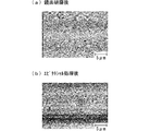
- FIG. 2 is an observation image showing a state in which convex defects are generated on the surface of the epitaxial wafer due to PID.
- FIG. 2 (a) is after mirror polishing
- FIG. 2 (b) is after epitaxial processing. Indicates the state.
- FIGS. 2A and 2B show, using the MAGICS, the surface of the silicon wafer after mirror polishing and the surface of the epitaxial wafer after completion of the epitaxial process through the cleaning process in the same field of view. The observed results are shown.
- the thickness of the epitaxial layer is 5 ⁇ m.
- the present invention has been completed on the basis of the above-mentioned knowledge, and the gist thereof is the following (1) silicon wafer cleaning method and (2) epitaxial wafer manufacturing method.
- the silicon wafer in the ozone gas treatment step, the silicon wafer is held in an ozone gas atmosphere, and in the hydrogen fluoride vapor treatment step, the silicon wafer is held in an atmosphere of hydrogen fluoride vapor. preferable.
- the cleaning method of (1) it is preferable that after the hydrogen fluoride vapor treatment step, a cleaning step of removing foreign matters remaining on the surface of the silicon wafer is performed.
- the silicon wafer in the cleaning step, can be subjected to ozone water treatment and dilute hydrofluoric acid treatment. After the ozone water treatment and dilute hydrofluoric acid treatment, pure water treatment is preferably performed.
- the PID before the epitaxial process, the PID is forcibly oxidized through an ozone gas treatment process, and the PID is dissolved and removed through a hydrogen fluoride vapor treatment process. Can do. For this reason, by performing an epitaxial process after that, it is possible to prevent the occurrence of convex defects due to PID on the surface of the epitaxial layer, and it is possible to manufacture an epitaxial wafer having excellent surface quality.
- FIG. 1 is a schematic diagram for explaining a situation in which convex defects are generated on the surface of an epitaxial wafer due to PID.
- FIG. 1 (a) is after mirror polishing
- FIG. 1 (b) is after cleaning
- FIG. (C) shows each state after the epitaxial treatment.
- FIG. 2 is an observation image showing a state in which convex defects are generated on the surface of the epitaxial wafer due to PID.
- FIG. 2 (a) is after mirror polishing
- FIG. 2 (b) is after epitaxial processing. Indicates the state.
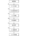
- FIG. 3 is a flowchart showing an example of processing steps in the silicon wafer cleaning method of the present invention.
- FIG. 3 is a flowchart showing an example of processing steps in the silicon wafer cleaning method of the present invention.
- FIG. 4 is a schematic diagram for explaining the behavior of PID when the silicon wafer cleaning method of the present invention is employed.
- FIG. 4 (a) is after mirror polishing
- FIG. 4 (b) is after cleaning
- FIG. (C) shows each state after the epitaxial treatment.
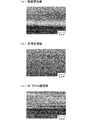
- FIG. 5 is an observation image of the wafer surface after each process in the present invention example
- FIG. 5 (a) is after mirror polishing
- FIG. 5 (b) is after the cleaning process
- FIG. 5 (c) is after the epitaxial process.
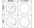
- FIG. 6 is a diagram showing the distribution of convex defects on the wafer surface after specular polishing and after epitaxial processing, divided into an example of the present invention and a comparative example.
- FIG. 3 is a flowchart showing an example of processing steps in the silicon wafer cleaning method of the present invention.
- ozone gas treatment is performed to oxidize the surface of the silicon wafer using ozone (O 3 ) gas.
- Ozone gas has a much higher O 3 concentration and significantly higher oxidizing power than ozone water used in a normal cleaning process.
- the O 3 concentration of ozone water is usually about 15 ppm (15 g / m 3 )
- the O 3 concentration of ozone gas is 105 g / m 3 or more.
- This ozone gas treatment can be efficiently performed by placing a silicon wafer in a sealed container and maintaining the inside of the container in an atmosphere of ozone gas.
- ozone gas can be sprayed onto the surface of a silicon wafer disposed in a sealed container during ozone gas treatment.
- step # 10 hydrogen fluoride vapor treatment is performed to dissolve and remove the oxidized surface of the silicon wafer after the ozone gas treatment using hydrogen fluoride (HF) vapor.
- HF hydrogen fluoride
- the PID that has become SiO 2 by the ozone gas treatment is dissolved and removed by the hydrogen fluoride vapor.
- hydrogen fluoride vapor has a much higher HF concentration and a significantly higher etching rate than dilute hydrofluoric acid used in a normal cleaning process.
- the HF concentration of dilute hydrofluoric acid is usually about 1 wt%
- the HF concentration of the hydrogen fluoride vapor stock solution is 48 wt% or more.
- Hydrogen fluoride vapor is generated by bubbling with nitrogen gas using this stock solution.
- This hydrogen fluoride vapor treatment can be performed efficiently by placing a silicon wafer in a sealed container and maintaining the container in an atmosphere of hydrogen fluoride vapor.
- the hydrogen fluoride vapor can be sprayed onto the surface of the silicon wafer disposed in the sealed container.
- step # 15 ozone water treatment is performed to oxidize the wafer surface using ozone water, and in step # 20, the oxide film on the wafer surface is removed using dilute hydrofluoric acid. Diluted hydrofluoric acid treatment is performed, and the wafer surface is cleaned by these. Further, in step # 25, the wafer surface is rinsed by pure water treatment using pure water, and finally, in step # 30, spin drying is performed.
- ozone water treatment, dilute hydrofluoric acid treatment and pure water treatment can be performed by immersing a silicon wafer in each treatment liquid or spraying each treatment liquid onto the wafer surface.
- ozone water treatment in step # 15 and the dilute hydrofluoric acid treatment in step # 20 can be alternately repeated, and the ozone water treatment in step # 15 is incorporated immediately before the pure water treatment in step # 25. You can also.
- the ozone water used in the ozone water treatment has an O 3 concentration of about 10 to 15 ppm (10 to 15 g / m 3 ).
- the dilute hydrofluoric acid used in the dilute hydrofluoric acid treatment has an HF concentration of 0.5 to 1 wt. % Can be used.
- the wafer surface can be cleaned by a treatment using a mixture of ozone water and dilute hydrofluoric acid.
- SC-1 cleaning solution in which ammonia water (NH 4 OH) and hydrogen peroxide (H 2 O 2 ) were mixed was used.
- the wafer surface may be cleaned by processing.
- an epitaxial process is performed.
- the cleaned silicon wafer is placed in a single-wafer reactor and heated to 1000 ° C. or more, and a raw material gas containing Si (eg, silicon tetrachloride (SiCl 4 ), trichlorosilane (SiHCl 3) )) And a carrier gas (eg, hydrogen (H 2 )) is introduced into the furnace.
- a raw material gas containing Si eg, silicon tetrachloride (SiCl 4 ), trichlorosilane (SiHCl 3)
- a carrier gas eg, hydrogen (H 2 )
- FIG. 4 is a schematic diagram for explaining the behavior of PID when the silicon wafer cleaning method of the present invention is employed.
- FIG. 4 (a) is after mirror polishing
- FIG. 4 (b) is after cleaning
- FIG. (C) shows each state after the epitaxial treatment.
- the silicon wafer 1 when the silicon wafer 1 is subjected to the epitaxial treatment after the ozone water treatment, the diluted hydrofluoric acid treatment, the pure water treatment and the spin drying treatment, the surface of the silicon wafer 1 is obtained as shown in FIG. In this case, the epitaxial layer 3 is vapor-phase grown over the entire region including the concave portion 6. As a result, the epitaxial wafer 2 can sufficiently ensure the surface quality without causing convex defects due to PID on the surface 3 a of the epitaxial layer 3.
- the silicon wafer 1 is more easily oxidized with ozone gas and more easily dissolved and removed by hydrogen fluoride vapor.
- the surface 3a of the epitaxial layer 3 can be flat without generating a dent at a position corresponding to the recess 6.
- the time required for the ozone gas treatment is not particularly defined, but if it is too short, forced oxidation of PID becomes insufficient, and therefore it is preferably 60 seconds or longer. More preferably, it is 150 seconds or more.
- the time required for the hydrogen fluoride vapor treatment is not particularly specified, but if the time is too short, the PID recessed portion becomes insufficient due to insufficient dissolution of the forcedly oxidized PID. It is preferable to set it to 2 seconds or more. On the other hand, if the time is too long, haze (roughness of the skin) occurs on the wafer surface.
- the silicon wafer cleaning method of the present invention is suitable for manufacturing an epitaxial wafer having a thin epitaxial layer thickness of 0.5 to 10 ⁇ m. Even if the PID exists on the wafer surface, the convex defects caused by the PID gradually flatten with the growth of the epitaxial layer, so that the convex defects caused by the PID occur when the epitaxial layer is thinner than when the epitaxial layer is thick. This is because it is easy to manifest.
- test wafers having a diameter of 300 mm subjected to mirror polishing were prepared, each test wafer was subjected to each treatment shown in FIG. 3 and washed, and thereafter an epitaxial treatment was performed.
- 60 seconds of ozone gas treatment and 120 seconds of hydrogen fluoride vapor treatment are performed, then 10 seconds of ozone water treatment and 3 seconds of dilute hydrofluoric acid treatment are repeated twice, and again 10 seconds of ozone water treatment.
- the pure water process for 10 seconds and the spin drying process for 25 seconds were performed.
- SiHCl 3 was used as the source gas
- the temperature in the reactor was set to 1130 ° C., and an epitaxial layer having a thickness of 5 ⁇ m was vapor-phase grown.
- test wafers having a diameter of 300 mm subjected to mirror polishing were prepared, and after cleaning each test wafer, an epitaxial process was performed.
- the ozone gas processing and the hydrogen fluoride vapor processing were omitted from the cleaning processing of the present invention example.
- the surface observation of each test wafer and the number of convex defects on the surface of each test wafer were investigated.
- FIG. 5 is an observation image of the wafer surface after each process in the present invention example, FIG. 5 (a) is after mirror polishing, FIG. 5 (b) is after the cleaning process, and FIG. 5 (c) is after the epitaxial process. Each state is shown.
- FIGS. 5A to 5C show the results of observing the same wafer after each processing in the same field of view.
- the PID generated by mirror polishing was removed by cleaning including ozone gas treatment and hydrogen fluoride vapor treatment, and it was confirmed that a recess was formed at that position (FIG. 5B). reference). Thereby, as shown in FIG.5 (c), it became clear that the convex defect resulting from PID did not generate
- FIG. 6 is a diagram showing the distribution of convex defects on the wafer surface after mirror polishing and after epitaxial processing, divided into an example of the present invention and a comparative example. As indicated by black dots in the figure, in the present invention example and the comparative example, PID occurred as convex defects over the entire area of the wafer surface after mirror polishing.
- PID can be forcibly oxidized by ozone gas treatment before the epitaxial treatment, and the PID can be dissolved and removed by hydrogen fluoride vapor treatment. Foreign matter remaining on the surface can be removed. For this reason, by performing an epitaxial process after that, it is possible to prevent the occurrence of convex defects due to PID on the surface of the epitaxial layer, and it is possible to manufacture an epitaxial wafer having excellent surface quality.
Landscapes
- Cleaning Or Drying Semiconductors (AREA)
- Mechanical Treatment Of Semiconductor (AREA)
- Crystals, And After-Treatments Of Crystals (AREA)
- Drying Of Semiconductors (AREA)
Abstract
Description
2:エピタキシャルウェーハ、 3:エピタキシャル層、
3a:エピタキシャル層の表面、 4:PID、
5:PID起因の凸欠陥、 6:凹部
Claims (5)
- シリコンウェーハに鏡面研磨を施した後、エピタキシャル層を形成する前にシリコンウェーハの表面を洗浄する方法であって、
オゾンガスを用いてシリコンウェーハの表面を酸化させるオゾンガス処理工程と、
フッ化水素蒸気を用いてシリコンウェーハの酸化した表面を溶解させ除去するフッ化水素蒸気処理工程と、を含むことを特徴とするシリコンウェーハの洗浄方法。 - 前記オゾンガス処理工程では、シリコンウェーハをオゾンガスの雰囲気中に保持し、前記フッ化水素蒸気処理工程では、シリコンウェーハをフッ化水素蒸気の雰囲気中に保持することを特徴とする請求項1に記載のシリコンウェーハの洗浄方法。
- 前記フッ化水素蒸気処理工程を経た後に、シリコンウェーハの表面に残存する異物を除去する洗浄工程を経ることを特徴とする請求項1または2に記載のシリコンウェーハの洗浄方法。
- 前記洗浄工程では、シリコンウェーハにオゾン水処理および希フッ酸処理を施すことを特徴とする請求項3に記載のシリコンウェーハの洗浄方法。
- 請求項1~4のいずれかに記載のシリコンウェーハの洗浄方法により洗浄したシリコンウェーハの表面に、エピタキシャル層を気相成長させることを特徴とするエピタキシャルウェーハの製造方法。
Priority Applications (4)
| Application Number | Priority Date | Filing Date | Title |
|---|---|---|---|
| JP2011519606A JP5278549B2 (ja) | 2009-06-26 | 2010-06-24 | シリコンウェーハの洗浄方法、およびその洗浄方法を用いたエピタキシャルウェーハの製造方法 |
| DE112010002718.8T DE112010002718B4 (de) | 2009-06-26 | 2010-06-24 | Verfahren zur reinigung eines siliciumwafers sowie verfahren zur herstellung eines epitaktischen wafers unter verwendung des reinigungsverfahrens |
| US13/378,065 US8664092B2 (en) | 2009-06-26 | 2010-06-24 | Method for cleaning silicon wafer, and method for producing epitaxial wafer using the cleaning method |
| KR1020127000711A KR101377240B1 (ko) | 2009-06-26 | 2010-06-24 | 실리콘 웨이퍼의 세정 방법 및, 그 세정 방법을 이용한 에피택셜 웨이퍼의 제조 방법 |
Applications Claiming Priority (2)
| Application Number | Priority Date | Filing Date | Title |
|---|---|---|---|
| JP2009152898 | 2009-06-26 | ||
| JP2009-152898 | 2009-06-26 |
Publications (1)
| Publication Number | Publication Date |
|---|---|
| WO2010150547A1 true WO2010150547A1 (ja) | 2010-12-29 |
Family
ID=43386332
Family Applications (1)
| Application Number | Title | Priority Date | Filing Date |
|---|---|---|---|
| PCT/JP2010/004204 Ceased WO2010150547A1 (ja) | 2009-06-26 | 2010-06-24 | シリコンウェーハの洗浄方法、およびその洗浄方法を用いたエピタキシャルウェーハの製造方法 |
Country Status (5)
| Country | Link |
|---|---|
| US (1) | US8664092B2 (ja) |
| JP (1) | JP5278549B2 (ja) |
| KR (1) | KR101377240B1 (ja) |
| DE (1) | DE112010002718B4 (ja) |
| WO (1) | WO2010150547A1 (ja) |
Cited By (3)
| Publication number | Priority date | Publication date | Assignee | Title |
|---|---|---|---|---|
| JP2014212213A (ja) * | 2013-04-18 | 2014-11-13 | 信越半導体株式会社 | シリコンウエーハの研磨方法およびエピタキシャルウエーハの製造方法 |
| JP2018164006A (ja) * | 2017-03-27 | 2018-10-18 | 信越半導体株式会社 | 貼り合わせウェーハの製造方法及び貼り合わせウェーハ |
| CN110681624A (zh) * | 2019-09-02 | 2020-01-14 | 山西烁科晶体有限公司 | 一种碳化硅单晶抛光片衬底的最终清洗方法 |
Families Citing this family (10)
| Publication number | Priority date | Publication date | Assignee | Title |
|---|---|---|---|---|
| CA2856196C (en) | 2011-12-06 | 2020-09-01 | Masco Corporation Of Indiana | Ozone distribution in a faucet |
| JP6312976B2 (ja) * | 2012-06-12 | 2018-04-18 | Sumco Techxiv株式会社 | 半導体ウェーハの製造方法 |
| WO2017112795A1 (en) | 2015-12-21 | 2017-06-29 | Delta Faucet Company | Fluid delivery system including a disinfectant device |
| JP6614076B2 (ja) * | 2016-09-07 | 2019-12-04 | 信越半導体株式会社 | 貼り合わせ用基板の表面欠陥の評価方法 |
| DE102017210450A1 (de) | 2017-06-21 | 2018-12-27 | Siltronic Ag | Verfahren, Steuerungssystem und Anlage zum Bearbeiten einer Halbleiterscheibe sowie Halbleiterscheibe |
| JP6773070B2 (ja) * | 2017-09-06 | 2020-10-21 | 信越半導体株式会社 | シリコンウェーハの評価方法及びシリコンウェーハの製造方法 |
| WO2019125810A1 (en) * | 2017-12-21 | 2019-06-27 | Globalwafers Co., Ltd. | Method of treating a single crystal silicon ingot to improve the lls ring/core pattern |
| JP7103211B2 (ja) | 2018-12-27 | 2022-07-20 | 株式会社Sumco | 半導体ウェーハの評価方法および製造方法ならびに半導体ウェーハの製造工程管理方法 |
| CN111254498B (zh) * | 2020-03-30 | 2021-03-26 | 常州时创能源股份有限公司 | 硅片酸抛光用添加剂及其应用 |
| CN112378546B (zh) * | 2020-10-09 | 2023-03-24 | 上海新昇半导体科技有限公司 | 一种检测高温腔体温度的方法 |
Citations (3)
| Publication number | Priority date | Publication date | Assignee | Title |
|---|---|---|---|---|
| JP2000331976A (ja) * | 1999-05-19 | 2000-11-30 | Kurita Water Ind Ltd | 基板の洗浄方法 |
| JP2007273911A (ja) * | 2006-03-31 | 2007-10-18 | Sumco Techxiv株式会社 | シリコンウェーハの製造方法 |
| JP2008159892A (ja) * | 2006-12-25 | 2008-07-10 | Univ Nagoya | パターン形成方法、および半導体装置の製造方法 |
Family Cites Families (14)
| Publication number | Priority date | Publication date | Assignee | Title |
|---|---|---|---|---|
| JPH0969509A (ja) * | 1995-09-01 | 1997-03-11 | Matsushita Electron Corp | 半導体ウェーハの洗浄・エッチング・乾燥装置及びその使用方法 |
| JPH10199847A (ja) * | 1997-01-08 | 1998-07-31 | Sony Corp | ウエハの洗浄方法 |
| JP3506172B2 (ja) | 1997-03-13 | 2004-03-15 | 信越半導体株式会社 | 半導体ウェーハのエッチング方法 |
| JP3088714B1 (ja) * | 1999-03-05 | 2000-09-18 | キヤノン販売株式会社 | 基板表面の清浄化方法及び半導体装置の製造方法 |
| JP2001176833A (ja) * | 1999-12-14 | 2001-06-29 | Tokyo Electron Ltd | 基板処理装置 |
| KR100416592B1 (ko) * | 2001-02-10 | 2004-02-05 | 삼성전자주식회사 | 매엽식 웨이퍼 세정 장치 및 이를 이용한 웨이퍼 세정 방법 |
| US6638863B2 (en) * | 2001-04-24 | 2003-10-28 | Acm Research, Inc. | Electropolishing metal layers on wafers having trenches or vias with dummy structures |
| KR100467016B1 (ko) * | 2002-05-30 | 2005-01-24 | 삼성전자주식회사 | 반도체기판의 세정방법 |
| US7051743B2 (en) * | 2002-10-29 | 2006-05-30 | Yong Bae Kim | Apparatus and method for cleaning surfaces of semiconductor wafers using ozone |
| JP2004281620A (ja) | 2003-03-14 | 2004-10-07 | Sony Corp | ウエハの洗浄方法 |
| DE102006020825A1 (de) * | 2006-05-04 | 2007-11-08 | Siltronic Ag | Verfahren zur Herstellung einer Schichtenstruktur |
| JP4696086B2 (ja) | 2007-02-20 | 2011-06-08 | 信越半導体株式会社 | シリコン単結晶ウエーハの仕上げ研磨方法及びシリコン単結晶ウエーハ |
| KR101106582B1 (ko) * | 2007-12-07 | 2012-01-19 | 가부시키가이샤 사무코 | 실리콘 웨이퍼 세정 방법 및 그 장치 |
| JP2009286683A (ja) * | 2008-06-02 | 2009-12-10 | Kyuchaku Gijutsu Kogyo Kk | 吸着剤を利用したオゾンの製造・貯蔵方法 |
-
2010
- 2010-06-24 KR KR1020127000711A patent/KR101377240B1/ko active Active
- 2010-06-24 DE DE112010002718.8T patent/DE112010002718B4/de active Active
- 2010-06-24 US US13/378,065 patent/US8664092B2/en active Active
- 2010-06-24 JP JP2011519606A patent/JP5278549B2/ja active Active
- 2010-06-24 WO PCT/JP2010/004204 patent/WO2010150547A1/ja not_active Ceased
Patent Citations (3)
| Publication number | Priority date | Publication date | Assignee | Title |
|---|---|---|---|---|
| JP2000331976A (ja) * | 1999-05-19 | 2000-11-30 | Kurita Water Ind Ltd | 基板の洗浄方法 |
| JP2007273911A (ja) * | 2006-03-31 | 2007-10-18 | Sumco Techxiv株式会社 | シリコンウェーハの製造方法 |
| JP2008159892A (ja) * | 2006-12-25 | 2008-07-10 | Univ Nagoya | パターン形成方法、および半導体装置の製造方法 |
Cited By (6)
| Publication number | Priority date | Publication date | Assignee | Title |
|---|---|---|---|---|
| JP2014212213A (ja) * | 2013-04-18 | 2014-11-13 | 信越半導体株式会社 | シリコンウエーハの研磨方法およびエピタキシャルウエーハの製造方法 |
| KR20150143506A (ko) | 2013-04-18 | 2015-12-23 | 신에쯔 한도타이 가부시키가이샤 | 실리콘 웨이퍼의 연마방법 및 에피택셜 웨이퍼의 제조방법 |
| US9824880B2 (en) | 2013-04-18 | 2017-11-21 | Shin-Etsu Handotai Co., Ltd | Method of polishing silicon wafer and method of producing epitaxial wafer |
| JP2018164006A (ja) * | 2017-03-27 | 2018-10-18 | 信越半導体株式会社 | 貼り合わせウェーハの製造方法及び貼り合わせウェーハ |
| CN110681624A (zh) * | 2019-09-02 | 2020-01-14 | 山西烁科晶体有限公司 | 一种碳化硅单晶抛光片衬底的最终清洗方法 |
| WO2021043167A1 (zh) * | 2019-09-02 | 2021-03-11 | 山西烁科晶体有限公司 | 一种碳化硅单晶抛光片衬底的最终清洗方法 |
Also Published As
| Publication number | Publication date |
|---|---|
| KR20120026126A (ko) | 2012-03-16 |
| JPWO2010150547A1 (ja) | 2012-12-10 |
| DE112010002718T5 (de) | 2012-08-09 |
| DE112010002718B4 (de) | 2019-11-21 |
| US20120100701A1 (en) | 2012-04-26 |
| KR101377240B1 (ko) | 2014-03-20 |
| US8664092B2 (en) | 2014-03-04 |
| JP5278549B2 (ja) | 2013-09-04 |
Similar Documents
| Publication | Publication Date | Title |
|---|---|---|
| JP5278549B2 (ja) | シリコンウェーハの洗浄方法、およびその洗浄方法を用いたエピタキシャルウェーハの製造方法 | |
| JP5888280B2 (ja) | シリコンウエーハの研磨方法およびエピタキシャルウエーハの製造方法 | |
| JP5018066B2 (ja) | 歪Si基板の製造方法 | |
| TW229324B (en) | Low cost method of fabricating epitaxial semiconductor devices | |
| EP1737026B1 (en) | Method of surface treating III-V semiconductor compound based substrates and method of manufacturing III-V compound semiconductors | |
| JP5029234B2 (ja) | エピタキシャルウェーハの製造方法 | |
| WO2013179569A1 (ja) | 半導体ウェーハの洗浄方法 | |
| KR20110036990A (ko) | 균일 산화막 형성 방법 및 세정 방법 | |
| JP2019102658A (ja) | シリコンウェーハの加工方法 | |
| JP4857738B2 (ja) | 半導体ウエーハの洗浄方法および製造方法 | |
| JP2012204369A (ja) | エピタキシャルウェーハの製造方法 | |
| TWI907748B (zh) | 半導體晶圓之清洗方法以及半導體晶圓之製造方法 | |
| JP7193026B1 (ja) | 洗浄液、及びウェーハの洗浄方法 | |
| JP2010171330A (ja) | エピタキシャルウェハの製造方法、欠陥除去方法およびエピタキシャルウェハ | |
| JPH1116844A (ja) | エピタキシャルシリコンウェーハの製造方法と素材用ウェーハ | |
| JP2002020200A (ja) | エピタキシャルシリコンウェーハの製造方法 | |
| JP5433927B2 (ja) | 貼り合わせウェーハの製造方法 | |
| WO1999050895A1 (en) | Method of manufacturing semiconductor wafer | |
| JP2010092938A (ja) | 半導体ウェハの洗浄方法、および、半導体ウェハ | |
| CN116798853A (zh) | 一种硅外延片的生长方法 | |
| JPH0878326A (ja) | エピタキシャルウェーハの製造方法 | |
| CN116213353A (zh) | 研磨后清洗方法 | |
| JP2006245301A (ja) | シリコンウェーハの製造方法 |
Legal Events
| Date | Code | Title | Description |
|---|---|---|---|
| 121 | Ep: the epo has been informed by wipo that ep was designated in this application |
Ref document number: 10791869 Country of ref document: EP Kind code of ref document: A1 |
|
| WWE | Wipo information: entry into national phase |
Ref document number: 2011519606 Country of ref document: JP |
|
| WWE | Wipo information: entry into national phase |
Ref document number: 13378065 Country of ref document: US |
|
| WWE | Wipo information: entry into national phase |
Ref document number: 1120100027188 Country of ref document: DE Ref document number: 112010002718 Country of ref document: DE |
|
| ENP | Entry into the national phase |
Ref document number: 20127000711 Country of ref document: KR Kind code of ref document: A |
|
| 122 | Ep: pct application non-entry in european phase |
Ref document number: 10791869 Country of ref document: EP Kind code of ref document: A1 |