WO2010143538A1 - 密封型半導体記録媒体及び密封型半導体記録装置 - Google Patents
密封型半導体記録媒体及び密封型半導体記録装置 Download PDFInfo
- Publication number
- WO2010143538A1 WO2010143538A1 PCT/JP2010/058970 JP2010058970W WO2010143538A1 WO 2010143538 A1 WO2010143538 A1 WO 2010143538A1 JP 2010058970 W JP2010058970 W JP 2010058970W WO 2010143538 A1 WO2010143538 A1 WO 2010143538A1
- Authority
- WO
- WIPO (PCT)
- Prior art keywords
- power
- coil
- data communication
- read
- semiconductor recording
- Prior art date
- Legal status (The legal status is an assumption and is not a legal conclusion. Google has not performed a legal analysis and makes no representation as to the accuracy of the status listed.)
- Ceased
Links
Images




Classifications
-
- H—ELECTRICITY
- H10—SEMICONDUCTOR DEVICES; ELECTRIC SOLID-STATE DEVICES NOT OTHERWISE PROVIDED FOR
- H10B—ELECTRONIC MEMORY DEVICES
- H10B20/00—Read-only memory [ROM] devices
-
- G—PHYSICS
- G06—COMPUTING OR CALCULATING; COUNTING
- G06K—GRAPHICAL DATA READING; PRESENTATION OF DATA; RECORD CARRIERS; HANDLING RECORD CARRIERS
- G06K19/00—Record carriers for use with machines and with at least a part designed to carry digital markings
- G06K19/06—Record carriers for use with machines and with at least a part designed to carry digital markings characterised by the kind of the digital marking, e.g. shape, nature, code
- G06K19/067—Record carriers with conductive marks, printed circuits or semiconductor circuit elements, e.g. credit or identity cards also with resonating or responding marks without active components
- G06K19/07—Record carriers with conductive marks, printed circuits or semiconductor circuit elements, e.g. credit or identity cards also with resonating or responding marks without active components with integrated circuit chips
- G06K19/077—Constructional details, e.g. mounting of circuits in the carrier
-
- H—ELECTRICITY
- H02—GENERATION; CONVERSION OR DISTRIBUTION OF ELECTRIC POWER
- H02J—ELECTRIC POWER NETWORKS; CIRCUIT ARRANGEMENTS OR SYSTEMS FOR SUPPLYING OR DISTRIBUTING ELECTRIC POWER; SYSTEMS FOR STORING ELECTRIC ENERGY
- H02J50/00—Circuit arrangements or systems for wireless supply or distribution of electric power
- H02J50/10—Circuit arrangements or systems for wireless supply or distribution of electric power using inductive coupling
-
- H—ELECTRICITY
- H04—ELECTRIC COMMUNICATION TECHNIQUE
- H04B—TRANSMISSION
- H04B5/00—Near-field transmission systems, e.g. inductive or capacitive transmission systems
- H04B5/20—Near-field transmission systems, e.g. inductive or capacitive transmission systems characterised by the transmission technique; characterised by the transmission medium
- H04B5/24—Inductive coupling
- H04B5/26—Inductive coupling using coils
-
- H—ELECTRICITY
- H04—ELECTRIC COMMUNICATION TECHNIQUE
- H04B—TRANSMISSION
- H04B5/00—Near-field transmission systems, e.g. inductive or capacitive transmission systems
- H04B5/20—Near-field transmission systems, e.g. inductive or capacitive transmission systems characterised by the transmission technique; characterised by the transmission medium
- H04B5/24—Inductive coupling
- H04B5/26—Inductive coupling using coils
- H04B5/263—Multiple coils at either side
-
- H—ELECTRICITY
- H04—ELECTRIC COMMUNICATION TECHNIQUE
- H04B—TRANSMISSION
- H04B5/00—Near-field transmission systems, e.g. inductive or capacitive transmission systems
- H04B5/20—Near-field transmission systems, e.g. inductive or capacitive transmission systems characterised by the transmission technique; characterised by the transmission medium
- H04B5/24—Inductive coupling
- H04B5/26—Inductive coupling using coils
- H04B5/266—One coil at each side, e.g. with primary and secondary coils
-
- H—ELECTRICITY
- H04—ELECTRIC COMMUNICATION TECHNIQUE
- H04B—TRANSMISSION
- H04B5/00—Near-field transmission systems, e.g. inductive or capacitive transmission systems
- H04B5/70—Near-field transmission systems, e.g. inductive or capacitive transmission systems specially adapted for specific purposes
- H04B5/72—Near-field transmission systems, e.g. inductive or capacitive transmission systems specially adapted for specific purposes for local intradevice communication
-
- H—ELECTRICITY
- H04—ELECTRIC COMMUNICATION TECHNIQUE
- H04B—TRANSMISSION
- H04B5/00—Near-field transmission systems, e.g. inductive or capacitive transmission systems
- H04B5/70—Near-field transmission systems, e.g. inductive or capacitive transmission systems specially adapted for specific purposes
- H04B5/79—Near-field transmission systems, e.g. inductive or capacitive transmission systems specially adapted for specific purposes for data transfer in combination with power transfer
-
- H—ELECTRICITY
- H10—SEMICONDUCTOR DEVICES; ELECTRIC SOLID-STATE DEVICES NOT OTHERWISE PROVIDED FOR
- H10B—ELECTRONIC MEMORY DEVICES
- H10B99/00—Subject matter not provided for in other groups of this subclass
-
- H—ELECTRICITY
- H02—GENERATION; CONVERSION OR DISTRIBUTION OF ELECTRIC POWER
- H02J—ELECTRIC POWER NETWORKS; CIRCUIT ARRANGEMENTS OR SYSTEMS FOR SUPPLYING OR DISTRIBUTING ELECTRIC POWER; SYSTEMS FOR STORING ELECTRIC ENERGY
- H02J7/00—Circuit arrangements for charging or discharging batteries or for supplying loads from batteries
- H02J7/40—Circuit arrangements for charging or discharging batteries or for supplying loads from batteries characterised by the exchange of charge or discharge related data
- H02J7/42—Circuit arrangements for charging or discharging batteries or for supplying loads from batteries characterised by the exchange of charge or discharge related data with electronic devices having internal batteries, e.g. mobile phones
Definitions
- the present invention relates to a sealed semiconductor recording medium and a sealed semiconductor recording device, for example, for supplying power to a sealed semiconductor recording medium that is completely isolated from the outside without affecting data communication.
- the present invention relates to a configuration and a configuration for reading out written data at high speed.
- a hard disk device that stores data using magnetism is said to have a lifetime of about 30 years. This is because failures often occur in the mechanical mechanism for bringing the data reading device closer to the disk that rotates at high speed.
- optical disk devices such as CD (Compact Disc), DVD, and Blu-ray Disc (registered trademark) are also said to have a lifetime of about 15 years. This is also because there are many failures in the rotating part, and the light transmittance decreases due to the aging of the material covering the disk surface.
- CD Compact Disc
- DVD DVD
- Blu-ray Disc registered trademark
- the digital recording device has a life of about several tens of years and will eventually break down. Therefore, digital information cannot be stored for a long time unless it is periodically copied to a new recording device. This operation is called migration.
- the cost for migration is high and the economic burden is large.
- the cost of digitally storing 3 copies of a 2 hour movie with 4K digital cinema quality (4096 x 2160 pixels, 24 frames per second) is said to be over 1 million yen per movie per year. Yes. Furthermore, it is said that it costs more than 20 million yen per movie per year to save all the fragmentary records made during the digital production process.
- Semiconductor integrated circuit devices such as mask ROMs are mainly manufactured using silicon and silicon oxide films and metals such as copper as raw materials. Silicon and silicon oxide films are very stable materials and have the feature that they do not change after 1000 years. On the other hand, metals oxidize, rust and corrode in a hot and humid environment.
- metal is used for circuit connection and is used inside a device covered with a silicon oxide film or a silicon nitride film.
- the metal contacts the outside of the device only in the openings of the silicon oxide film and the silicon nitride film called pads for wiring connection (wire bonding) to the outside of the device for power supply and data communication. If moisture permeates into the device through this opening, the internal metal wiring will also corrode and eventually cause a failure.
- the contact type mask ROM is more resistant to environmental changes and noise such as radiation (cosmic rays) and electromagnetic (geomagnetic), and the data is long-term unless the metal wiring corrodes. It has the feature that it can be stored.
- the mask ROM is sealed with a silicon oxide film or silicon nitride film without opening the pad as in the above proposal, it is possible to prevent moisture from entering the inside of the device from the outside. It is predicted that this is possible.
- FIG. 13 is an explanatory diagram of the humidity dependence of the chip life according to a research report on the life of the chip (for example, see Non-Patent Document 2). As shown in FIG. 13, if the humidity inside the chip can be reduced to 2% or less, the lifetime of the chip becomes 1000 years or more even when the temperature of the chip is 100 ° C.
- CMOS technology As of 2009, if 45nm CMOS technology is used, a 4-gigabit mask ROM can be manufactured on a 1 cm square chip at a cost of about 200 yen. Therefore, if four 15 inch ( ⁇ 38 cm) wafers are stacked, a 2.5 terabit mask ROM can be manufactured at about 140,000 yen.
- the remaining technical problem is how to supply power to the sealed mask ROM and read the data.
- a technique for reading data wirelessly while feeding power wirelessly a technique called a radio tag (RFID: Radio Frequency IDentification) is used.
- RFID Radio Frequency IDentification
- the data reading speed of the wireless tag is about 250 kilobits per second. Therefore, it takes 115 days or more to read out 2.5 terabit digital information. In order to read this out in about 2 hours, a communication speed of several hundred megabits per second, which is about 1000 times faster, is required.
- data communication is performed by placing data when the tag reflects the electromagnetic wave while the reader supplies power to the tag.
- This method is called a backscatter method (modulation back diffusion method).
- backscatter method modulation back diffusion method
- an antenna used for power supply and communication
- a capacitor used for power storage and a tag chip are connected by wiring on a printed circuit board.
- Patent Documents 1 to Patent Document 7 and Non-Patent Document 3 to Non-Patent Document 9). If this technology is used, the communication speed can be increased to gigabits per second or more.
- Patent Document 5 proposes that a chip test is performed by inductive coupling between a chip and a test head in an LSI chip test apparatus.
- the communication distance between the reader, which is a power supply source and a data communication source, and the stone, which is a sealed semiconductor recording medium needs to be at least 0.5 mm, and 3 mm is sufficient.
- the wafer can be thinned to about 50 ⁇ m because the thickness of a protective film such as a SiN film is necessary.
- the diameter of the data communication coil needs to be about 2 mm.
- a pair of coils is required for data communication and its timing clock signal, and when preparing for communication from stone to leader and for communication from leader to stone respectively, a total of four coils are required. I need it.
- the coupling coefficient k of the data communication coil (the ratio of coupling of the transmission / reception coils is 1 when the coupling is complete, and when the coupling is completely uncoupled) Is about 0.15), and the voltage signal generated in the receiving coil is about 150 mV. Therefore, when the coil is smaller than 2 mm when the communication distance is 1 mm, the value of k becomes remarkably small, the received signal voltage becomes remarkably small, and data communication cannot be performed.
- the diameter of the power feeding coil is required to be about 6 mm.
- k is about 0.4.
- the ratio (P RX / P TX ) between the power P TX received by Stone and the power P RX transmitted by the reader is about the square of k.
- the upper limit of the transmission power of the reader is given by V DD 2 / R, where R is the impedance of the power transmission circuit.
- the chip size needs to be at least 22 mm ⁇ 14 mm.
- the semiconductor integrated circuit has a problem that the manufacturing yield is remarkably lowered when the maximum side is a chip larger than 20 mm. Further, generally, when the maximum side of a chip exceeds 20 mm, it becomes impossible to perform exposure with a single reticle, so that it is necessary to connect a plurality of reticles, resulting in an increase in cost and an increase in defect probability. Therefore, it is necessary to obtain a certain high yield for cost reduction, and for that purpose, the maximum dimension of the chip must be smaller than 20 mm.
- the capacitance value is insufficient for a capacitor that can be mounted on a semiconductor chip, power is sent by placing it on an AC signal by magnetic field coupling, and when the received AC signal is converted to a DC signal by a rectifier circuit, the AC component is There is a problem that it cannot be made small enough.
- Non-Patent Document 1 the power supply of each chip is shared. However, if the power supply of each chip is shared, a defect of one chip is caused by all chips sharing the power supply. It may cause malfunction. For example, if there is a short circuit failure between power supplies, the power supply voltage is not sufficiently high in all chips sharing the power supply, causing a problem that the circuit cannot operate normally.
- an object of the present invention is to provide a sealed and highly reliable semiconductor memory that can supply power wirelessly and perform high-speed data communication wirelessly without mutual interference at low cost.
- a sealed semiconductor recording medium of the present invention is provided with a plurality of read-only memory blocks having a maximum side of 20 mm or less on at least one semiconductor substrate in a state in which power supply wiring is not shared with each other.
- Each read-only memory block includes a power receiving coil and a data communication coil, and data written in each read-only memory block is different from each other.
- the block size corresponding to the chip size has a maximum side of 20 mm or less, so that it is possible to produce a sealed semiconductor recording medium at a low cost by using a manufacturing technique with high reliability.
- a failure of one read-only memory block does not cause a malfunction of all the read-only memory blocks sharing the power source.
- each read-only memory block further includes time division means for performing power reception and data communication in a time division manner.
- the time-sharing means since the time-sharing means is provided, power reception and data communication can be performed in a time-sharing manner, whereby the power supply electromagnetic wave and the data communication electromagnetic wave may interfere with each other. Therefore, the bit error rate of data communication can be set within an allowable range.
- the power receiving coil and the data communication coil can be arranged close to each other, and the maximum side can be 20 mm or less, for example, about 15 mm ⁇ 15 mm.
- each read-only memory block further includes smoothing means for smoothing the AC power received by the power receiving coil, and in particular, the power receiving coil. It is desirable to have a mechanism for smoothing the AC power received in step 1 by shifting the phases thereof.
- the smoothing means it is possible to store the supplied AC power as DC power in the parasitic capacitance of the wiring portion constituting the mask ROM.
- the ratio of the ripple of the power supply voltage to the power supply voltage V DD can be suppressed to 10% or less. As a result, the circuit can operate normally.
- the semiconductor substrate is further sealed with a silicon nitride film.
- Non-Patent Document 2 a lifetime of 1000 years or more is expected.
- the read-only memory blocks are arranged in the same array, and the data written in the read-only memory blocks are different from each other on the semiconductor substrates.
- a plurality of dedicated memory blocks are stacked so as to overlap in a projective manner.
- the recording capacity can be increased in accordance with the number of stacked layers.
- the sealed semiconductor recording device of the present invention is provided with a plurality of reader blocks each including the above-described sealed semiconductor recording medium, a power supply coil for supplying power to the sealed semiconductor recording medium, and a data communication coil.
- One reader block may be provided in the reader, but by providing a plurality of reader blocks, the data reading speed can be increased in proportion to the number of reader blocks.
- the power supply coil, the data communication coil provided in each reader block, the power supply coil provided in each read-only memory block, and the data It is desirable that the distance between the coils for communication is 3 mm or less.
- a sealed high-reliability semiconductor memory capable of supplying power wirelessly and performing high-speed data communication wirelessly without mutual interference Can be provided at low cost.
- 1 is a conceptual configuration diagram of a sealed semiconductor recording device according to an embodiment of the present invention. It is a conceptual explanatory drawing of electric power communication and a data communication structure.
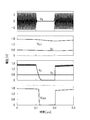
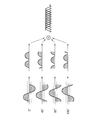
- 1 is a conceptual cross-sectional view of a sealed semiconductor recording device according to Embodiment 1 of the present invention. It is a top view which shows an example of a ROM block and a leader block. It is a configuration explanatory view of a mask ROM. It is a circuit block diagram for electric power communication and data communication of Example 1 of this invention. It is composition explanatory drawing of a full wave rectifier and a power sensor. It is explanatory drawing of the time change of each output in FIG. It is explanatory drawing of 4 channel full wave rectification.
- FIG. 1 is a conceptual perspective view of a sealed semiconductor recording device according to an embodiment of the present invention, which is composed of a digital rosette stone 10 storing data and a reader 30 for reading the stored data.
- a mask 11 In the digital rosetta stone 10, a mask 11, a wafer 11 on which a ROM block 20 in which a power receiving coil 21, a data communication coil 22, and a wireless communication circuit are integrated is arranged, the positions of the ROM blocks 20 overlap each other in a projective manner.
- a plurality of such layers are laminated and sealed with a protective film 12 such as SiN or SiO 2 .
- the reader 30 is a reader in which a power supply coil 32 and a data communication coil 33 having the same shape corresponding to the power receiving coil 21 and the data communication coil 22 provided on the wafer 11 and a data wireless communication circuit are integrated.
- the same number of blocks 31 as the ROM blocks 20 are arranged.
- the power supply coil 21 provided in the ROM block 20 of each stage of the wafer 11 is projected and overlapped with the power supply coil 32 sequentially. Received with attenuation. The same applies to electromagnetic waves for data communication.
- the number of reader blocks 31 provided in the reader 30 is at least one and at most the same number as the ROM block 20, and the data reading speed can be increased in proportion to the number of reader blocks 31.
- the number of reader blocks 31 is smaller than the number of ROM blocks 20, data is read from each ROM block 20 by moving the reader 30 on the digital rosette stone 10.
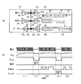
- FIG. 2 is an explanatory diagram of a power communication and data communication configuration.
- 2A is a conceptual circuit block diagram for power communication and data communication
- FIG. 2B is a chart diagram of power communication and data communication system.
- the power supply coil 32 in the leader block 31 side and the transmitting coil 33 1 and the receiver coil 33 2 is provided as a data communication coils, each coil , power amplifier 34, the transmission amplifier 35 1 and the receiver amplifier 35 2 are respectively connected.
- the ROM block 20 is provided with a power supply coil 21, a reception coil 22 1 and a transmission coil 22 2 as data communication coils, and each coil includes a power rectifier 23 and a reception amplifier. 24 1 and a transmission amplifier 24 2 are connected to each other.
- the power rectifier 23 is connected to a capacitor 25 that charges the supplied power, and is also connected to a power sensor 26 and a power-on reset circuit 27.
- the capacitor 25 is obtained by adding a capacitance parasitic to the power supply line of the circuit of the ROM block 20 or a capacitance created by using, for example, a MOSFET gate capacitance.
- Each of the reception amplifier 24 1 and the transmitter amplifier 24 2 registers 28 1, 28 2 are connected, each register 28 1, 28 2 are connected to the mask ROM 29.
- M DATA mask ROM
- the fourth procedure (IV) power supply from the leader block 31 to the ROM block 20 is stopped.
- the ROM block 20 detects, by starting the wireless transmitter wirelessly transmits the data stored in the register 28 2 data to the leader block 31.
- the wireless transmitter operates using the energy stored in the capacitor 25. Accordingly, although the value of V DD gradually decreases, the time of the fourth procedure is determined from the power consumption of the circuit so that the value of V DD does not decrease below a predetermined value.
- Ripple V ratio V R / V DD for V DD of R of the power supply voltage that remains when the power receiving coil for converting an AC signal generated in the DC voltage by the rectifier circuit, to be suppressed to 10% or less.
- V R / V DD becomes 10% or more, the circuit does not operate normally.
- the impedance R of the circuit of the mask ROM is about 25 ⁇ , for example.
- a failure of one ROM block can cause malfunction of all ROM blocks sharing the power supply. For example, if there is a short circuit failure between power supplies, the power supply voltage is not sufficiently high in all ROM blocks sharing the power supply, and the circuit cannot operate normally.
- the ROM blocks are electrically isolated from each other in the present invention, even if one ROM block malfunctions, the data can be completely restored by redundantly encoding and storing the data. Can do. For example, if a Low Density Parity Check (LDPC) code is used, restoration can be performed by increasing the data amount by 23%.
- LDPC Low Density Parity Check
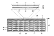
- FIG. 3 is a cross-sectional view of the sealed semiconductor recording device according to the first embodiment of the present invention, and includes a digital rosette stone 40 that stores data and a reader 60 that reads the stored data.
- the wafer 41 in which the ROM block 50 in which the mask ROM, the power receiving coil 51, the data communication coil 52, and the wireless communication circuit are integrated is arranged in each ROM as shown in FIG.
- a plurality of blocks 50 are stacked such that the positions of the blocks 50 are projected and overlapped, and sealed with a SiN protective film 42.
- Each wafer 41 is individually covered with a SiN protective film 43, and each wafer 41 is laminated by a substrate bonding technique using an SiO 2 film 44.
- the reader 60 is a reader in which a power supply coil 62 and a data communication coil 63 having the same shape corresponding to the power receiving coil 51 and the data communication coil 52 provided on the wafer 41 and a data wireless communication circuit are integrated.
- the same number of blocks 61 as the ROM blocks 50 are arranged.
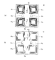
- FIG. 4 is a plan view showing an example of a ROM block and a reader block.
- FIG. 4A is a plan view of a ROM block.
- four power receiving coils 51 1 to 514 having a side of 6 mm are arranged in a ROM block 50 having a size of 15 mm ⁇ 15 mm, and one side is 1 side. .4 4 mm data communication coils 52 1 to 52 4 are arranged in a cross shape. Of the four data communication coils 52 1 to 52 4 , two are for transmission and the other two are for reception.
- FIG. 4B is a plan view of the leader block.
- four power supply coils 62 1 to 624 having a side of 6 mm are arranged on a leader block 61 having a size of 15 mm ⁇ 15 mm, and one side is one.
- .4 4 mm data communication coils 63 1 to 63 4 are arranged in a cross shape. Of the four data communication coils 63 1 to 63 4 , two are for transmission and the other two are for reception. At this time, the communication distance between the leader block 61 and the ROM block 50 is 0.6 mm.
- the power receiving coil 62 and the data communication coil 63 are effectively the same size and the same arrangement as the power receiving coil 51 and the data communication coil 52 provided in the ROM block 50, respectively.
- FIG. 5 is an explanatory diagram of the configuration of the mask ROM
- FIG. 5 (a) is a schematic plan view
- FIG. 5 (b) is an equivalent circuit diagram.
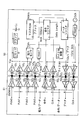
- FIG. 6 is a circuit block diagram for power communication and data communication according to the first embodiment of the present invention.
- the power supply coils 62 1 to 62 4 and the power supply coils 51 1 to 51 4 face each other.
- the data communication coils 63 3 and 63 4 for transmission and the data communication coils 52 2 and 52 1 for reception face each other, and the data communication coils 63 1 and 63 2 for reception and data communication for transmission are transmitted.
- Coils 52 4 and 52 3 are opposed to each other.
- each data communication coil is composed of a pair of coils for data communication and its timing clock signal.
- a clock M clk of 100 MHz is used for reading the mask ROM
- a clock D clk of 1 GHz is used to wirelessly transmit data in the data register from the ROM block 50 to the reader block 60.
- clocks oscillate and output only when necessary, and stop when unnecessary to avoid unnecessary power consumption.
- Several clocks immediately after the start of clock oscillation may have a small amplitude or a large jitter, so circuits Mask 1 and Mask 2 are used to prevent the use of this.
- the number of clocks is counted by a counter, and the first and second clocks are not used, and the third and subsequent clocks are used.
- FIG. 7A is a circuit configuration diagram of a full-wave rectifier as an example of the power rectifier Prx (see, for example, Non-Patent Document 10).
- FIG. 7B is a configuration diagram of the power sensor, and detects whether the wireless power transmission from the leader block to the ROM block is started or stopped. The power transmission wave received by the ROM block is converted from alternating current to direct current using the full-wave rectifier shown in FIG.
- V S decreases and becomes lower than the potential VC of 1/3 of V DD.
- the ROM block detects that the power supply output V SEN changes to low and power transmission is stopped.
- V S rises and becomes higher than the potential V C that is 1/3 of V DD , V SEN changes to high, and power transmission is resumed.
- the ROM block detects this. In this case, it is desirable to use a hysteresis comparator in which the comparison threshold has hysteresis characteristics so that the comparator does not malfunction due to noise.
- FIG. 9 is an explanatory diagram of 4-channel full-wave rectification.
- a plurality of communication channels are used for power transmission from the leader block 61 to the ROM block 50, and the fluctuations (ripples) in the power supply voltage V DD of the received and rectified ROM block 50 are reduced by shifting the phases of the channels from each other. .
- Fig. 10 shows the result of actually producing a chip with a coil size reduced to 1/3 for power feeding test, setting the communication distance to 1/3, and wirelessly feeding power using 4 power channels. It is explanatory drawing.
- the test was conducted by setting one side of the power coil provided on the 5 mm square chip to 2 mm and setting the distance between the leader block and the ROM block to 0.2 mm.
- the power necessary for 100 MHz operation of the mask ROM can be wirelessly fed, and at the same time, the maximum ripple voltage V R of the power supply voltage converted to DC becomes 33.6 mV, which can be reduced to 2% or less of V DD. It was verified by experiment.
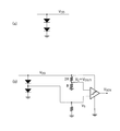
- FIG. 11A is a circuit diagram showing an example of the clamp circuit shown in FIG. 6, and assuming that the forward voltage drop of the diode is 0.6 V, 1.2 V is obtained by connecting two diodes in series.
- a clamp circuit can be configured. That is, when the power supply voltage V DD becomes 1.2 V, the diode causes a current to flow in the forward direction and suppresses an increase in V DD .
- This diode may be replaced with a MOSFET having a gate and drain connected.
- FIG. 11B is an example of a circuit that detects that the clamp circuit has started to operate.
- V S becomes higher than V DD / 3 and V SEN goes high.
- the supplied power becomes excessive, heat is generated with the power discarded in the clamp circuit.
- the leader block side is notified by wireless communication that the supplied power is excessive, and feedback control is performed to reduce the transmission power of the leader block.
- a sealed semiconductor recording device according to a second embodiment of the present invention will be described with reference to FIG. 12.
- the basic configuration is the same as that of the first embodiment except that the coil arrangement is different. Only the coil arrangement will be described.
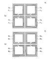
- FIG. 12 is a conceptual plan view of a ROM block and a reader block according to the second embodiment of the present invention.
- FIG. 12A is a conceptual plan view of a ROM block.
- four power receiving coils 71 1 to 714 having a side of 7 mm are arranged on a ROM block 70 having a size of 15 mm ⁇ 15 mm, and one side
- Four data communication coils 72 1 to 724 having a diameter of 6 mm are arranged concentrically inside the power receiving coils 71 1 to 71 4 .
- the four data communication coils 72 1 to 72 4 two are for transmission and the other two are for reception.
- FIG. 12B is a conceptual plan view of a leader block.
- four power supply coils 82 1 to 82 4 each having a side of 7 mm are arranged on a leader block 81 having a size of 15 mm ⁇ 15 mm.
- Four data communication coils 83 1 to 83 4 having a diameter of 6 mm are arranged concentrically inside the power supply coils 82 1 to 82 4 .
- the four data communication coils 83 1 to 83 4 two are for transmission and the other two are for reception.
- the data communication coil 72 1 on the upper left side in the figure (one of them is inverted and faces opposite, so the data communication coil 83 4 on the upper right side) and the data communication coil 72 3 on the lower right side
- the data communication coil 83 2 on the lower left is assigned to the data communication and timing communication for communication from the leader to the stone
- the data communication coil 72 4 on the upper right (also the data communication coil on the upper left) 83 1 ) and the data communication coil 72 2 on the lower left side are preferably assigned to data communication and timing communication for communication from the stone to the reader.
- the communication from the leader to the stone and the communication from the stone to the leader are made time-sharing, so that the pair of data communication coils and the timing data communication coils that are communicating at the same time are not horizontally adjacent but one diagonally. Since the distance is about 4 times, the interference between the data communication coils can be further reduced.
- the data communication coil can be arranged inside the power coil. It becomes possible.
- the size of the data communication coil can be increased, so that the distance between the reader and the digital rosette stone can be increased. For example, reading can be performed with an interval of 3 mm.
Landscapes
- Engineering & Computer Science (AREA)
- Computer Networks & Wireless Communication (AREA)
- Signal Processing (AREA)
- Power Engineering (AREA)
- Computer Hardware Design (AREA)
- Microelectronics & Electronic Packaging (AREA)
- Physics & Mathematics (AREA)
- General Physics & Mathematics (AREA)
- Theoretical Computer Science (AREA)
- Near-Field Transmission Systems (AREA)
- Semiconductor Integrated Circuits (AREA)
- Semiconductor Memories (AREA)
Abstract
Description
PRX/PTX≒k2 =0.42 =0.16
になる。したがって、通信距離が1mmのときに、直径が6mmよりも小さなコイルを用いると、kの値が著しく小さくなり、受信電力が著しく小さくなって、ストーンの回路に十分な電力を供給できなくなる。
VDD 2 /R=1.82 /5≒650mW
になる。
第1手順(I):まず、リーダーブロック31からROMブロック20に磁界結合を用いて電力を無線送電する。給電された電力はチップ上に形成されたキャパシタ25に蓄えられる。ROMブロック20の電源の電位VDDが所定の電位まで上昇したことを電力センサ26を用いて検出し、パワー・オン・リセット回路27を用いてシステムをリセットする。
VR/VDD=1/(fCR)
で求められる。
VR/VDD=1/(fCR)=1/(250MHz×1nF×25Ω)≒0.16
であり、16%になる。つまり、マスクROMの回路ではリップルが大きくなるので、この問題を解決するために、本発明では、電力送信を複数のチャネルに分け、各チャネルの電磁波の位相をずらすことでリップルを低減する。
Claims (9)
- 少なくとも1枚の半導体基板に最大辺が20mm以下のサイズの複数の読出専用メモリブロックを互いに電源配線を共有しない状態で設け、
前記各読出専用メモリブロックは電力受給用コイルとデータ通信用コイルを備えるとともに、
前記各読出専用メモリブロックに書き込まれたデータが互いに異なっている密封型半導体記録媒体。 - 前記各読出専用メモリブロックは、電力の受給とデータ通信とを時間分割して行う時分割手段を備えている請求項1に記載の密封型半導体記録媒体。
- 前記各読出専用メモリブロックは、前記電力受給用コイルで受給した交流電力を平滑化する平滑化手段を備えている請求項1に記載の密封型半導体記録媒体。
- 前記平滑化手段が、前記電力受給用コイルで受給した交流電力の位相を互いにずらして平滑化する機構を備えている請求項3に記載の密封型半導体記録媒体。
- 前記読出専用メモリブロックが、前記電力受給用コイルに供給された電力が予め設定した値より過剰になったことを前記データ通信用コイルに伝達するフィードバック制御機構を備えている請求項1に記載の密封型半導体記録媒体。
- 前記半導体基板が、シリコン窒化膜で密封されている請求項1に記載の密封型半導体記録媒体。
- 前記各読出専用メモリブロックが同じ配列で配置されるとともに、前記各読出専用メモリブロックに書き込まれたデータが互いに異なる半導体基板を、前記各読出専用メモリブロックが投影的に重なるように複数枚積層した請求項1に記載の密封型半導体記録媒体。
- 請求項1に記載の密封型半導体記録媒体と、
前記密封型半導体記録媒体に電力を供給する電力供給用コイルとデータ通信用コイルとを備えたリーダーブロックを複数設けた半導体基板からなるリーダーとを有し、
前記各リーダーブロックに設けた電力供給用コイルとデータ通信用コイルと前記各読出専用メモリブロックに設けた電力受給用コイルとデータ通信用コイルとがそれぞれ互いに投影的に重なるように対向させた密封型半導体記録装置。 - 前記各リーダーブロックに設けた電力供給用コイルとデータ通信用コイルと前記各読出専用メモリブロックに設けた電力受給用コイルとデータ通信用コイルとの対向間隔が3mm以下である請求項8に記載の密封型半導体記録装置。
Priority Applications (1)
| Application Number | Priority Date | Filing Date | Title |
|---|---|---|---|
| US13/377,677 US8827166B2 (en) | 2009-06-12 | 2010-05-27 | Sealed semiconductor recording medium and sealed semiconductor memory |
Applications Claiming Priority (2)
| Application Number | Priority Date | Filing Date | Title |
|---|---|---|---|
| JP2009141403A JP5374246B2 (ja) | 2009-06-12 | 2009-06-12 | 密封型半導体記録媒体及び密封型半導体記録装置 |
| JP2009-141403 | 2009-06-12 |
Publications (1)
| Publication Number | Publication Date |
|---|---|
| WO2010143538A1 true WO2010143538A1 (ja) | 2010-12-16 |
Family
ID=43308793
Family Applications (1)
| Application Number | Title | Priority Date | Filing Date |
|---|---|---|---|
| PCT/JP2010/058970 Ceased WO2010143538A1 (ja) | 2009-06-12 | 2010-05-27 | 密封型半導体記録媒体及び密封型半導体記録装置 |
Country Status (4)
| Country | Link |
|---|---|
| US (1) | US8827166B2 (ja) |
| JP (1) | JP5374246B2 (ja) |
| KR (1) | KR101628759B1 (ja) |
| WO (1) | WO2010143538A1 (ja) |
Cited By (1)
| Publication number | Priority date | Publication date | Assignee | Title |
|---|---|---|---|---|
| JP2013214242A (ja) * | 2012-04-03 | 2013-10-17 | Isd Corp | 密封型半導体記憶装置およびこれを用いた記憶システム |
Families Citing this family (14)
| Publication number | Priority date | Publication date | Assignee | Title |
|---|---|---|---|---|
| US8035401B2 (en) | 2007-04-18 | 2011-10-11 | Cypress Semiconductor Corporation | Self-calibrating driver for charging a capacitive load to a desired voltage |
| EP2617207A2 (en) * | 2010-09-17 | 2013-07-24 | Cascade Microtech, Inc. | Systems and methods for non-contact power and data transfer in electronic devices |
| JP5791326B2 (ja) * | 2011-03-30 | 2015-10-07 | 学校法人慶應義塾 | 積層集積回路装置 |
| KR20130081620A (ko) | 2012-01-09 | 2013-07-17 | 주식회사 케이더파워 | 무선 충전 시스템용 수신기 |
| US9509375B2 (en) | 2013-08-01 | 2016-11-29 | SK Hynix Inc. | Wireless transceiver circuit with reduced area |
| EP3231148B1 (en) * | 2015-04-24 | 2019-08-07 | Hewlett-Packard Development Company, L.P. | Routing signals based on an orientation of devices with respect to each other |
| US10571487B2 (en) | 2016-11-30 | 2020-02-25 | Formfactor Beaverton, Inc. | Contact engines, probe head assemblies, probe systems, and associated methods for on-wafer testing of the wireless operation of a device under test |
| TWI665869B (zh) * | 2018-07-23 | 2019-07-11 | 華邦電子股份有限公司 | 輸入接收器電路及適應性回授方法 |
| US10778164B2 (en) | 2018-10-05 | 2020-09-15 | Winbond Electronics Corp. | Input receiver circuit and adaptive feedback method |
| JP7214758B2 (ja) | 2019-11-15 | 2023-01-30 | キオクシア株式会社 | ストレージデバイスおよびストレージシステム |
| WO2021095232A1 (ja) | 2019-11-15 | 2021-05-20 | キオクシア株式会社 | ストレージシステム及びウェハ |
| EP4060721A4 (en) | 2019-11-15 | 2023-08-09 | Kioxia Corporation | STORAGE DEVICE AND CONTROL METHOD |
| WO2022044161A1 (ja) | 2020-08-26 | 2022-03-03 | キオクシア株式会社 | ストレージウェハ及びストレージウェハの製造方法 |
| US12306243B2 (en) | 2023-06-12 | 2025-05-20 | Formfactor, Inc. | Space transformers configured to be utilized in a probe system, probe systems that include the space transformers, and related methods |
Citations (9)
| Publication number | Priority date | Publication date | Assignee | Title |
|---|---|---|---|---|
| JP2000068892A (ja) * | 1998-08-25 | 2000-03-03 | Matsushita Electric Ind Co Ltd | 質問器アンテナ、カードアンテナ及びそれらを用いた質問器、非接触icカード |
| JP2003521904A (ja) * | 2000-02-11 | 2003-07-22 | バイオ メディック データシステムズ インコーポレイテッド | 移植可能な誘電的にプログラムされる温度検出トランスポンダ |
| JP2005228981A (ja) * | 2004-02-13 | 2005-08-25 | Keio Gijuku | 電子回路 |
| JP2006072826A (ja) * | 2004-09-03 | 2006-03-16 | Matsushita Electric Ind Co Ltd | 無線タグシステム、リーダライタ、無線タグ装置およびデータの書き込み・読み出し方法 |
| JP2006127363A (ja) * | 2004-11-01 | 2006-05-18 | Advance Design Corp | 非接触ic媒体 |
| JP2006320182A (ja) * | 2005-05-16 | 2006-11-24 | Matsushita Electric Works Ltd | 給電システム、給電制御装置、給電装置、及び給電方法 |
| JP2006330961A (ja) * | 2005-05-25 | 2006-12-07 | Dainippon Printing Co Ltd | 情報記録媒体と情報記録媒体の使用方法 |
| JP2007034711A (ja) * | 2005-07-27 | 2007-02-08 | Brother Ind Ltd | 無線通信媒体及び無線通信装置並びに無線通信システム |
| JP2009087229A (ja) * | 2007-10-02 | 2009-04-23 | Sharp Corp | 半導体記憶装置および記憶システム |
Family Cites Families (9)
| Publication number | Priority date | Publication date | Assignee | Title |
|---|---|---|---|---|
| JP4193060B2 (ja) | 2004-06-04 | 2008-12-10 | 学校法人慶應義塾 | 電子回路 |
| JP4677598B2 (ja) | 2004-08-05 | 2011-04-27 | 学校法人慶應義塾 | 電子回路 |
| JP4124365B2 (ja) | 2004-08-24 | 2008-07-23 | 学校法人慶應義塾 | 電子回路 |
| JP5024740B2 (ja) | 2004-09-30 | 2012-09-12 | 学校法人慶應義塾 | Lsiチップ試験装置 |
| JP2006173986A (ja) | 2004-12-15 | 2006-06-29 | Keio Gijuku | 電子回路 |
| JP2006173415A (ja) | 2004-12-16 | 2006-06-29 | Keio Gijuku | 電子回路 |
| EP2199954B1 (en) * | 2007-10-02 | 2012-09-12 | Sharp Kabushiki Kaisha | Semiconductor storage device and storage system |
| JP5491868B2 (ja) * | 2007-11-26 | 2014-05-14 | 学校法人慶應義塾 | 電子回路 |
| JP5475962B2 (ja) * | 2008-04-28 | 2014-04-16 | 学校法人慶應義塾 | 電子回路 |
-
2009
- 2009-06-12 JP JP2009141403A patent/JP5374246B2/ja active Active
-
2010
- 2010-05-27 KR KR1020117028109A patent/KR101628759B1/ko active Active
- 2010-05-27 US US13/377,677 patent/US8827166B2/en active Active
- 2010-05-27 WO PCT/JP2010/058970 patent/WO2010143538A1/ja not_active Ceased
Patent Citations (9)
| Publication number | Priority date | Publication date | Assignee | Title |
|---|---|---|---|---|
| JP2000068892A (ja) * | 1998-08-25 | 2000-03-03 | Matsushita Electric Ind Co Ltd | 質問器アンテナ、カードアンテナ及びそれらを用いた質問器、非接触icカード |
| JP2003521904A (ja) * | 2000-02-11 | 2003-07-22 | バイオ メディック データシステムズ インコーポレイテッド | 移植可能な誘電的にプログラムされる温度検出トランスポンダ |
| JP2005228981A (ja) * | 2004-02-13 | 2005-08-25 | Keio Gijuku | 電子回路 |
| JP2006072826A (ja) * | 2004-09-03 | 2006-03-16 | Matsushita Electric Ind Co Ltd | 無線タグシステム、リーダライタ、無線タグ装置およびデータの書き込み・読み出し方法 |
| JP2006127363A (ja) * | 2004-11-01 | 2006-05-18 | Advance Design Corp | 非接触ic媒体 |
| JP2006320182A (ja) * | 2005-05-16 | 2006-11-24 | Matsushita Electric Works Ltd | 給電システム、給電制御装置、給電装置、及び給電方法 |
| JP2006330961A (ja) * | 2005-05-25 | 2006-12-07 | Dainippon Printing Co Ltd | 情報記録媒体と情報記録媒体の使用方法 |
| JP2007034711A (ja) * | 2005-07-27 | 2007-02-08 | Brother Ind Ltd | 無線通信媒体及び無線通信装置並びに無線通信システム |
| JP2009087229A (ja) * | 2007-10-02 | 2009-04-23 | Sharp Corp | 半導体記憶装置および記憶システム |
Cited By (1)
| Publication number | Priority date | Publication date | Assignee | Title |
|---|---|---|---|---|
| JP2013214242A (ja) * | 2012-04-03 | 2013-10-17 | Isd Corp | 密封型半導体記憶装置およびこれを用いた記憶システム |
Also Published As
| Publication number | Publication date |
|---|---|
| KR20120031164A (ko) | 2012-03-30 |
| JP5374246B2 (ja) | 2013-12-25 |
| US20120091211A1 (en) | 2012-04-19 |
| KR101628759B1 (ko) | 2016-06-09 |
| US8827166B2 (en) | 2014-09-09 |
| JP2010287113A (ja) | 2010-12-24 |
Similar Documents
| Publication | Publication Date | Title |
|---|---|---|
| JP5374246B2 (ja) | 密封型半導体記録媒体及び密封型半導体記録装置 | |
| TW488001B (en) | Semiconductor device, manufacturing method thereof, and semiconductor substrate | |
| JP5325495B2 (ja) | 半導体装置及びその製造方法 | |
| TW503464B (en) | IC card | |
| TWI442513B (zh) | 半導體裝置的製造方法 | |
| CN101040289A (zh) | 具有组合式无功耦合器的rfid装置 | |
| US20140014732A1 (en) | Coupling in and to rfid smart cards | |
| KR20150021898A (ko) | 차지 펌프 회로, 및 그 차지 펌프 회로를 구비한 반도체 장치 | |
| US20120217658A1 (en) | Multi-stack semiconductor integrated circuit device | |
| JP2006172122A (ja) | カード状記憶装置 | |
| JP5483764B2 (ja) | 半導体装置 | |
| TWI230395B (en) | Lamination type semiconductor device | |
| KR101003116B1 (ko) | 패드를 제어하는 반도체 메모리 장치 및 그 장치가 장착된 멀티칩 패키지 | |
| JP4269502B2 (ja) | データキャリア | |
| TW200304265A (en) | Rectifier utilizing a grounded antenna | |
| CN101221629A (zh) | 智能卡芯片以及放置输入/输出焊盘的方法 | |
| KR20140110619A (ko) | 반도체 패키지 | |
| US6368901B2 (en) | Integrated circuit wireless tagging | |
| CN114639663A (zh) | 包括层叠的半导体芯片的半导体封装件 | |
| Yuxiang et al. | Digital rosetta stone: A sealed permanent memory with inductive-coupling power and data link | |
| TW200809640A (en) | Magnetic sheet, antenna system, and method of manufacturing antenna system | |
| EP2907134A2 (en) | Memory device with reduced on-chip noise | |
| US8426956B2 (en) | Semiconductor package structure having plural packages in a stacked arrangement | |
| KR100843887B1 (ko) | 집적회로 및 그 정보 기록 방법 | |
| JPH08226967A (ja) | 強フィールドプログラム可能なトランスポンダシステムおよび方法 |
Legal Events
| Date | Code | Title | Description |
|---|---|---|---|
| 121 | Ep: the epo has been informed by wipo that ep was designated in this application |
Ref document number: 10786069 Country of ref document: EP Kind code of ref document: A1 |
|
| ENP | Entry into the national phase |
Ref document number: 20117028109 Country of ref document: KR Kind code of ref document: A |
|
| NENP | Non-entry into the national phase |
Ref country code: DE |
|
| WWE | Wipo information: entry into national phase |
Ref document number: 13377677 Country of ref document: US |
|
| 122 | Ep: pct application non-entry in european phase |
Ref document number: 10786069 Country of ref document: EP Kind code of ref document: A1 |