WO2010113831A1 - 発光素子材料前駆体およびその製造方法 - Google Patents
発光素子材料前駆体およびその製造方法 Download PDFInfo
- Publication number
- WO2010113831A1 WO2010113831A1 PCT/JP2010/055502 JP2010055502W WO2010113831A1 WO 2010113831 A1 WO2010113831 A1 WO 2010113831A1 JP 2010055502 W JP2010055502 W JP 2010055502W WO 2010113831 A1 WO2010113831 A1 WO 2010113831A1
- Authority
- WO
- WIPO (PCT)
- Prior art keywords
- group
- aryl
- hydrogen
- light emitting
- formula
- Prior art date
Links
- 0 **c(c(*)c1*)c(c(*)c2*)c3c1c(*)c(*1CC1)c1c(*)c(*)c(*)c2c31 Chemical compound **c(c(*)c1*)c(c(*)c2*)c3c1c(*)c(*1CC1)c1c(*)c(*)c(*)c2c31 0.000 description 5
Images

Classifications
-
- C—CHEMISTRY; METALLURGY
- C07—ORGANIC CHEMISTRY
- C07D—HETEROCYCLIC COMPOUNDS
- C07D519/00—Heterocyclic compounds containing more than one system of two or more relevant hetero rings condensed among themselves or condensed with a common carbocyclic ring system not provided for in groups C07D453/00 or C07D455/00
-
- H—ELECTRICITY
- H10—SEMICONDUCTOR DEVICES; ELECTRIC SOLID-STATE DEVICES NOT OTHERWISE PROVIDED FOR
- H10K—ORGANIC ELECTRIC SOLID-STATE DEVICES
- H10K85/00—Organic materials used in the body or electrodes of devices covered by this subclass
- H10K85/60—Organic compounds having low molecular weight
-
- C—CHEMISTRY; METALLURGY
- C07—ORGANIC CHEMISTRY
- C07C—ACYCLIC OR CARBOCYCLIC COMPOUNDS
- C07C49/00—Ketones; Ketenes; Dimeric ketenes; Ketonic chelates
- C07C49/587—Unsaturated compounds containing a keto groups being part of a ring
- C07C49/657—Unsaturated compounds containing a keto groups being part of a ring containing six-membered aromatic rings
- C07C49/683—Unsaturated compounds containing a keto groups being part of a ring containing six-membered aromatic rings having unsaturation outside the aromatic rings
-
- C—CHEMISTRY; METALLURGY
- C07—ORGANIC CHEMISTRY
- C07D—HETEROCYCLIC COMPOUNDS
- C07D209/00—Heterocyclic compounds containing five-membered rings, condensed with other rings, with one nitrogen atom as the only ring hetero atom
- C07D209/56—Ring systems containing three or more rings
- C07D209/80—[b, c]- or [b, d]-condensed
- C07D209/82—Carbazoles; Hydrogenated carbazoles
- C07D209/86—Carbazoles; Hydrogenated carbazoles with only hydrogen atoms, hydrocarbon or substituted hydrocarbon radicals, directly attached to carbon atoms of the ring system
-
- C—CHEMISTRY; METALLURGY
- C07—ORGANIC CHEMISTRY
- C07D—HETEROCYCLIC COMPOUNDS
- C07D307/00—Heterocyclic compounds containing five-membered rings having one oxygen atom as the only ring hetero atom
- C07D307/77—Heterocyclic compounds containing five-membered rings having one oxygen atom as the only ring hetero atom ortho- or peri-condensed with carbocyclic rings or ring systems
- C07D307/91—Dibenzofurans; Hydrogenated dibenzofurans
-
- C—CHEMISTRY; METALLURGY
- C07—ORGANIC CHEMISTRY
- C07D—HETEROCYCLIC COMPOUNDS
- C07D333/00—Heterocyclic compounds containing five-membered rings having one sulfur atom as the only ring hetero atom
- C07D333/50—Heterocyclic compounds containing five-membered rings having one sulfur atom as the only ring hetero atom condensed with carbocyclic rings or ring systems
- C07D333/76—Dibenzothiophenes
-
- C—CHEMISTRY; METALLURGY
- C09—DYES; PAINTS; POLISHES; NATURAL RESINS; ADHESIVES; COMPOSITIONS NOT OTHERWISE PROVIDED FOR; APPLICATIONS OF MATERIALS NOT OTHERWISE PROVIDED FOR
- C09K—MATERIALS FOR MISCELLANEOUS APPLICATIONS, NOT PROVIDED FOR ELSEWHERE
- C09K11/00—Luminescent, e.g. electroluminescent, chemiluminescent materials
- C09K11/06—Luminescent, e.g. electroluminescent, chemiluminescent materials containing organic luminescent materials
-
- H—ELECTRICITY
- H10—SEMICONDUCTOR DEVICES; ELECTRIC SOLID-STATE DEVICES NOT OTHERWISE PROVIDED FOR
- H10K—ORGANIC ELECTRIC SOLID-STATE DEVICES
- H10K50/00—Organic light-emitting devices
- H10K50/10—OLEDs or polymer light-emitting diodes [PLED]
- H10K50/11—OLEDs or polymer light-emitting diodes [PLED] characterised by the electroluminescent [EL] layers
-
- H—ELECTRICITY
- H10—SEMICONDUCTOR DEVICES; ELECTRIC SOLID-STATE DEVICES NOT OTHERWISE PROVIDED FOR
- H10K—ORGANIC ELECTRIC SOLID-STATE DEVICES
- H10K71/00—Manufacture or treatment specially adapted for the organic devices covered by this subclass
- H10K71/10—Deposition of organic active material
- H10K71/18—Deposition of organic active material using non-liquid printing techniques, e.g. thermal transfer printing from a donor sheet
-
- H—ELECTRICITY
- H10—SEMICONDUCTOR DEVICES; ELECTRIC SOLID-STATE DEVICES NOT OTHERWISE PROVIDED FOR
- H10K—ORGANIC ELECTRIC SOLID-STATE DEVICES
- H10K85/00—Organic materials used in the body or electrodes of devices covered by this subclass
- H10K85/60—Organic compounds having low molecular weight
- H10K85/615—Polycyclic condensed aromatic hydrocarbons, e.g. anthracene
- H10K85/622—Polycyclic condensed aromatic hydrocarbons, e.g. anthracene containing four rings, e.g. pyrene
-
- C—CHEMISTRY; METALLURGY
- C07—ORGANIC CHEMISTRY
- C07C—ACYCLIC OR CARBOCYCLIC COMPOUNDS
- C07C2602/00—Systems containing two condensed rings
- C07C2602/36—Systems containing two condensed rings the rings having more than two atoms in common
- C07C2602/42—Systems containing two condensed rings the rings having more than two atoms in common the bicyclo ring system containing seven carbon atoms
-
- C—CHEMISTRY; METALLURGY
- C07—ORGANIC CHEMISTRY
- C07C—ACYCLIC OR CARBOCYCLIC COMPOUNDS
- C07C2602/00—Systems containing two condensed rings
- C07C2602/50—Spiro compounds
-
- C—CHEMISTRY; METALLURGY
- C07—ORGANIC CHEMISTRY
- C07C—ACYCLIC OR CARBOCYCLIC COMPOUNDS
- C07C2603/00—Systems containing at least three condensed rings
- C07C2603/02—Ortho- or ortho- and peri-condensed systems
- C07C2603/04—Ortho- or ortho- and peri-condensed systems containing three rings
- C07C2603/22—Ortho- or ortho- and peri-condensed systems containing three rings containing only six-membered rings
- C07C2603/24—Anthracenes; Hydrogenated anthracenes
-
- C—CHEMISTRY; METALLURGY
- C09—DYES; PAINTS; POLISHES; NATURAL RESINS; ADHESIVES; COMPOSITIONS NOT OTHERWISE PROVIDED FOR; APPLICATIONS OF MATERIALS NOT OTHERWISE PROVIDED FOR
- C09K—MATERIALS FOR MISCELLANEOUS APPLICATIONS, NOT PROVIDED FOR ELSEWHERE
- C09K2211/00—Chemical nature of organic luminescent or tenebrescent compounds
- C09K2211/10—Non-macromolecular compounds
- C09K2211/1003—Carbocyclic compounds
- C09K2211/1011—Condensed systems
-
- C—CHEMISTRY; METALLURGY
- C09—DYES; PAINTS; POLISHES; NATURAL RESINS; ADHESIVES; COMPOSITIONS NOT OTHERWISE PROVIDED FOR; APPLICATIONS OF MATERIALS NOT OTHERWISE PROVIDED FOR
- C09K—MATERIALS FOR MISCELLANEOUS APPLICATIONS, NOT PROVIDED FOR ELSEWHERE
- C09K2211/00—Chemical nature of organic luminescent or tenebrescent compounds
- C09K2211/10—Non-macromolecular compounds
- C09K2211/1018—Heterocyclic compounds
- C09K2211/1025—Heterocyclic compounds characterised by ligands
- C09K2211/1029—Heterocyclic compounds characterised by ligands containing one nitrogen atom as the heteroatom
-
- C—CHEMISTRY; METALLURGY
- C09—DYES; PAINTS; POLISHES; NATURAL RESINS; ADHESIVES; COMPOSITIONS NOT OTHERWISE PROVIDED FOR; APPLICATIONS OF MATERIALS NOT OTHERWISE PROVIDED FOR
- C09K—MATERIALS FOR MISCELLANEOUS APPLICATIONS, NOT PROVIDED FOR ELSEWHERE
- C09K2211/00—Chemical nature of organic luminescent or tenebrescent compounds
- C09K2211/10—Non-macromolecular compounds
- C09K2211/1018—Heterocyclic compounds
- C09K2211/1025—Heterocyclic compounds characterised by ligands
- C09K2211/1088—Heterocyclic compounds characterised by ligands containing oxygen as the only heteroatom
-
- C—CHEMISTRY; METALLURGY
- C09—DYES; PAINTS; POLISHES; NATURAL RESINS; ADHESIVES; COMPOSITIONS NOT OTHERWISE PROVIDED FOR; APPLICATIONS OF MATERIALS NOT OTHERWISE PROVIDED FOR
- C09K—MATERIALS FOR MISCELLANEOUS APPLICATIONS, NOT PROVIDED FOR ELSEWHERE
- C09K2211/00—Chemical nature of organic luminescent or tenebrescent compounds
- C09K2211/10—Non-macromolecular compounds
- C09K2211/1018—Heterocyclic compounds
- C09K2211/1025—Heterocyclic compounds characterised by ligands
- C09K2211/1092—Heterocyclic compounds characterised by ligands containing sulfur as the only heteroatom
Definitions
- the present invention relates to a precursor of a light emitting device material useful as a constituent material of an organic electroluminescence (hereinafter “EL”) device, a method for producing the precursor, and a light emitting device using the precursor.
- EL organic electroluminescence
- the technical field is light-emitting element materials used for light-emitting elements that can be used in fields such as display elements, flat panel displays, backlights, lighting, interiors, signs, signboards, electrophotographic machines, and optical signal generators. is there.
- This light-emitting element is characterized by being thin and capable of emitting light with high luminance under a low driving voltage, and being capable of multicolor light emission by selecting a light-emitting element material.
- the manufacturing method of an organic EL element can be classified into the following two types.
- the vacuum deposition method is a method of forming a film on a device substrate by sublimating a low molecular material in a vacuum. According to this method, it is possible to manufacture a device in which a plurality of types of materials are stacked while controlling a desired film thickness (see Non-Patent Document 1). A practical and high-performance organic EL element can be obtained by this manufacturing method.
- the manufacturing apparatus is expensive and the ratio of the material to be formed on the substrate to the material used is low.
- Non-Patent Document 2 Wet processes typified by spin coating, ink jet, and nozzle coating methods make it easy to fabricate large area devices that require improved material utilization and patterning.
- Non-Patent Document 2 since only a material having sufficient solubility in a solvent suitable for the process can be used, it is difficult to use the low molecular material that realizes a high-performance organic EL element as it is. Therefore, the organic EL element currently produced by the wet process is often inferior in element performance as compared with that produced by the vacuum deposition method.
- Patent Literature a technique has been developed in which a solution containing a soluble precursor is applied to a device substrate, formed into a film, and then subjected to heat treatment to convert it into an organic semiconductor material, thereby obtaining desired characteristics.
- Patent Literature 1 to 3
- JP 2003-304014 A (US Patent Publication No. 2003-226996) JP 2005-232136 A JP 2008-135198 A
- Patent Documents 1 to 3 there are limitations on the compounds that can produce soluble precursors by the methods described in Patent Documents 1 to 3. For example, it could not be applied to anthracene derivatives having substituents at the 9,10 positions, pyrene derivatives, and 4-substituted tetracene derivatives exemplified by rubrene.
- An object of the present invention is to solve such a problem, and to make it possible to produce a soluble precursor of a light emitting device material (hereinafter referred to as “light emitting device material precursor”), which has not been obtained conventionally,
- the present invention provides a material suitable for a wet process and a method for manufacturing an organic EL element using the material.
- the present invention comprises the following contents.
- R 1 to R 6 may be the same as or different from each other, hydrogen, alkyl group, cycloalkyl group, alkenyl group, cycloalkenyl group, alkoxy group, alkylthio group, aryl ether group, aryl thioether group, aryl Selected from the group consisting of a group and a heteroaryl group, provided that at least one of R 1 to R 6 has two or more condensed aromatic hydrocarbons.
- it is a manufacturing method of the said light emitting element material precursor, Comprising: It consists of the following structures.
- the step of obtaining the compound represented by the formula (8) by the reaction of substituting the R 171 from the compound represented by the following formula (7), the protecting group of the compound represented by the formula (8) thus obtained is removed.
- a step of converting the compound represented by the formula (9) into a compound represented by the formula (10) by an oxidation reaction to the compound represented by the formula (9) by a reaction to form a compound represented by the formula (9) A method for producing a [2,2,2] -cyclooctadiene-2,3-dione derivative.
- R 170 is an aryl group or a heteroaryl group.
- R 171 is an electron-withdrawing group.
- R 172 to R 176 are hydrogen, an alkyl group, a cycloalkyl group, an alkenyl group, a cycloalkenyl group, an alkoxy group, an alkylthio group.
- Aryl ether group, aryl thioether group, aryl group, heteroaryl group and halogen, R 177 to R 178 are selected from hydrogen, alkyl group, alkoxy group, aryl group and aryl ether group.
- a device can be manufactured by applying and forming a solution containing a light emitting element material precursor by an inkjet method or a nozzle coating method, and then performing a conversion process to a device constituent material.
- Sectional drawing which shows an example of the organic EL element by which the light emitting layer was patterned by this invention
- the light emitting device material precursor of the present invention is represented by the general formula (1).
- R 1 to R 6 may be the same or different and are each hydrogen, alkyl group, cycloalkyl group, alkenyl group, cycloalkenyl group, aryl group, alkoxy group, aryl ether group, alkylthio group, arylthioether group , A heteroaryl group and a halogen. However, at least one of R 1 to R 6 has two or more condensed aromatic hydrocarbons.
- a preferred light emitting device material precursor is represented by the general formula (1 ').
- R 1 to R 6 are the same as those in the formula (1). However, at least one of R 1 to R 6 has three or more condensed aromatic hydrocarbons.
- the light emitting device material precursor represented by the formula (1) is [2,2,2] -bicyclooctadiene-2,3-dione to which R 1 to R 6 are bonded.
- the light emitting element material precursor described below also has [2,2,2] -bicyclooctadiene-2,3-dione as a skeleton. These light emitting element material precursors emit two molecules of carbon monoxide upon irradiation with light, change their structure, and convert into light emitting element materials. [2,2,2] -Bicyclooctadiene-2,3-dione is converted into a benzene ring while the substituent remains bonded to carbon.
- the structure changes, and converted into a light emitting device material.
- the light emitting element material precursor of the present invention can suppress aggregation of molecules by having a bulky bicyclo structure site in the molecule, the solubility in a solvent is improved as a result.
- the present invention is particularly effective when a light-emitting element material containing condensed aromatic hydrocarbons is aimed. That is, a condensed aromatic hydrocarbon having a large number of condensed rings has a low affinity for a polar solvent because of its small molecular polarity.
- a condensed aromatic hydrocarbon having a large number of condensed rings has a low affinity for a polar solvent because of its small molecular polarity.
- the action of suppressing the aggregation of molecules by the bulky bicyclo structure is particularly effective for improving the solubility of a compound having a condensed aromatic hydrocarbon having a large number of condensed rings in a nonpolar solvent.
- a light-emitting device material precursor of a compound such as an anthracene derivative or pyrene derivative having a substituent at the 9-position or the 10-position which was difficult to realize by the conventional method, can be produced. It is possible to apply a compound suitable as a wet process.
- the alkyl group represents, for example, a saturated aliphatic hydrocarbon group such as a methyl group, an ethyl group, an n-propyl group, an isopropyl group, an n-butyl group, a sec-butyl group, and a tert-butyl group. It may or may not have.
- the preferred carbon number of the alkyl group is in the range of 1-20.
- the additional substituent when it is substituted and examples thereof include an alkyl group, an aryl group, and a heteroaryl group.
- a cycloalkyl group shows saturated alicyclic hydrocarbon groups, such as a cyclopropyl group, a cyclohexyl group, a norbornyl group, and an adamantyl group, for example.
- the cycloalkyl group preferably has 3 to 20 carbon atoms.
- the cycloalkyl group may or may not have a substituent.
- alkenyl group refers to an unsaturated aliphatic hydrocarbon group containing a double bond such as a vinyl group, an allyl group, or a butadienyl group.
- the alkenyl group preferably has 2 to 20 carbon atoms.
- the alkenyl group may or may not have a substituent.
- the cycloalkenyl group refers to an unsaturated alicyclic hydrocarbon group containing a double bond such as a cyclopentenyl group, a cyclopentadienyl group, or a cyclohexenyl group.
- the preferred carbon number of the cycloalkenyl group is in the range of 3-20. This may or may not have a substituent.
- An aryl group is an aromatic group such as a phenyl group, a naphthyl group, a biphenyl group, a fluorenyl group, a phenanthryl group, a terphenyl group, an anthracenyl group and a pyrenyl group.
- the aryl group preferably has 6 to 40 carbon atoms.
- the aryl group may be unsubstituted or substituted.
- Substituents that such an aryl group may have are alkyl, cycloalkyl, alkenyl, alkynyl, alkoxy, aryl ether, alkylthio, halogen, cyano, amino, silyl, and boryl.
- the alkoxy group refers to a functional group in which an aliphatic hydrocarbon group is bonded through an ether bond such as a methoxy group, an ethoxy group, and a propoxy group.
- the alkoxy group preferably has 1 to 20 carbon atoms. This aliphatic hydrocarbon group may or may not have a substituent.
- An aryl ether group refers to a functional group to which an aromatic hydrocarbon group is bonded via an ether bond, such as a phenoxy group.
- the aryl ether group preferably has 6 to 40 carbon atoms.
- the aromatic hydrocarbon group may or may not have a substituent.
- the alkylthio group is a group in which an oxygen atom of an ether bond of an alkoxy group is substituted with a sulfur atom.
- the alkylthio group preferably has 1 to 20 carbon atoms.
- the hydrocarbon group of the alkylthio group may or may not have a substituent.
- the aryl thioether group is a group in which an oxygen atom of an ether bond of an aryl ether group is substituted with a sulfur atom.
- the arylthioether group preferably has 1 to 20 carbon atoms.
- the aromatic hydrocarbon group in the arylthio group may or may not have a substituent.
- the heteroaryl group refers to an aromatic group having atoms other than carbon such as furanyl group, thiophenyl group, oxazolyl group, pyridyl group, quinolinyl group, carbazolyl group in the ring.
- the heteroaryl group preferably has 2 to 30 carbon atoms.
- the aromatic group may or may not have a substituent.
- Halogen is fluorine, chlorine, bromine, iodine or the like.
- the condensed aromatic hydrocarbon is an aromatic compound composed of carbon and hydrogen, and has a structure in which one side of a benzene ring is shared by two rings, such as naphthalene.
- the condensed ring having two or more rings include naphthalene, anthracene, triphenylene, phenanthrene, tetracene, pyrene, chrysene, pentacene, perylene, coronene and the like.
- those other than the group having two or more condensed aromatic hydrocarbons are preferably hydrogen or an aryl group among the above substituents, and particularly preferably all of them are hydrogen atoms.
- the diketo bridging unit of the formula (1) forms a benzene ring by releasing carbon monoxide. Therefore, when all of R 1 to R 6 other than a group having two or more condensed aromatic hydrocarbons are hydrogen atoms, they are converted into phenyl groups. That is, a derivative of a condensed aromatic hydrocarbon compound having two or more rings and having a substituent having a phenyl group at the terminal can be obtained.
- At least one of R 1 to R 6 in the general formula (1) or the general formula (1 ′) is represented by the general formulas (2-1) to (2-7) from the light emission characteristics of the light emitting device material. And those containing any of the skeletons represented by
- R 10 to R 17 , R 20 to R 27 , R 30 to R 37 , R 40 to R 49 , R 50 to R 61 , R 70 to R 81 and R 82 to R 89 may be the same or different and are each a hydrogen atom, an alkyl group, a cycloalkyl group, a heterocyclic group, an alkenyl group, a cycloalkenyl group, an alkynyl group, an alkoxy group, an alkylthio group, an aryl ether group, an arylthioether Group, aryl group, heteroaryl group, halogen, cyano group, carbonyl group, carboxyl group, oxycarbonyl group, carbamoyl group, amino group, silyl group, phosphine oxide group and adjacent substituents Chosen from the inside.
- X 1 to X 6 , Y 1 to Y 4 and Z 1 to Z 2 may be the same or different and are each hydrogen, an alkyl group, a cycloalkyl group, a heterocyclic group, an alkenyl group, a cycloalkenyl group, an alkynyl group, Alkoxy group, alkylthio group, aryl ether group, aryl thioether group, aryl group, heteroaryl group, halogen, cyano group, carbonyl group, carboxyl group, oxycarbonyl group, carbamoyl group, amino group, silyl group, phosphine oxide group and adjacent It is selected from the condensed rings formed between the substituents.
- R 82 to R 89 are each a diketo bridging unit in the formula (1) via a direct bond or a linking group. Used for connection.
- the heterocyclic group refers to an aliphatic ring having atoms other than carbon, such as a pyran ring, a piperidine ring, and a cyclic amide, in the ring, which may or may not have a substituent. .
- the heterocyclic group preferably has 2 to 20 carbon atoms.
- the alkynyl group indicates, for example, an unsaturated aliphatic hydrocarbon group containing a triple bond such as an ethynyl group, which may or may not have a substituent.
- the alkynyl group preferably has 2 to 20 carbon atoms.
- a carbonyl group refers to a substituent containing a carbon-oxygen double bond such as an acyl group or a formyl group.
- An acyl group is a substituent in which hydrogen of a formyl group is substituted with an alkyl group, an aryl group, or a heteroaryl group.
- the oxycarbonyl group is a substituent containing an ether bond on the carbon of the carbonyl group, such as t-butyloxycarbonyl group or benzyloxycarbonyl group.
- the preferred carbon number of the carbonyl group is in the range of 1-20.
- the carbamoyl group refers to a substituent from which the hydroxyl group of carbamic acid is removed, and may or may not have a substituent.
- the preferred carbon number of the carbamoyl group is in the range of 1-20.
- the amino group represents a nitrogen compound group such as a dimethylamino group, which may be unsubstituted or substituted.
- the amino group preferably has 0 to 20 carbon atoms.
- the silyl group refers to, for example, a silicon compound group such as a trimethylsilyl group, which may be unsubstituted or substituted.
- the preferred carbon number of the silyl group is in the range of 1-20.
- the phosphine oxide group is a substituent containing a phosphorus-oxygen double bond, which may be unsubstituted or substituted.
- the phosphine oxide group preferably has 1 to 20 carbon atoms.
- the condensed ring formed between adjacent substituents will be described by exemplifying the general formula (2-1).
- two adjacent substituents selected from R 10 to R 17 are bonded to each other to form a conjugated or non-serving condensed ring.
- This condensed ring may contain a nitrogen, oxygen, or sulfur atom in the ring structure, or may be further bonded to another ring.
- the light-emitting element material precursor of the present invention is preferably represented by the general formula (3) or (4) from the viewpoint of the light emission characteristics of the light-emitting element material after conversion and the durability of the element.
- R 90 to R 99 may be the same as or different from each other, and hydrogen, alkyl group, cycloalkyl group, heterocyclic group, alkenyl group, cycloalkenyl group, alkynyl group, alkoxy group, alkylthio group, aryl ether group , Arylthioether group, aryl group, heteroaryl group, halogen, cyano group, carbonyl group, carboxyl group, oxycarbonyl group, carbamoyl group, amino group, silyl group, phosphine oxide group and adjacent substituents Selected from fused rings.
- R 100 to R 105 may be the same or different and are each hydrogen, alkyl group, cycloalkyl group, alkenyl group, cycloalkenyl group, alkoxy group, alkylthio group, aryl ether group, aryl thioether group, aryl group, heteroaryl Selected from the group and halogen.
- A is selected from a single bond, an arylene group, and a heteroarylene group.
- m is an integer of 1 to 3. Any m of R 90 to R 99 is used for connection with A. Any one of R 100 to R 105 is used for connection with A.
- R 110 to R 119 may be the same or different and are each a hydrogen atom, an alkyl group, a cycloalkyl group, a heterocyclic group, an alkenyl group, a cycloalkenyl group, an alkynyl group, an alkoxy group, an alkylthio group, an aryl ether group.
- R 120 to R 125 may be the same or different and each represents hydrogen, an alkyl group, a cycloalkyl group, an alkenyl group, a cycloalkenyl group, an alkoxy group, an alkylthio group, an aryl ether group, an aryl thioether group, an aryl group, a heteroaryl Selected from the group and halogen.
- B is selected from a single bond, an arylene group, and a heteroarylene group.
- n is an integer of 1 to 2. Any n of R 120 to R 125 and any n of R 110 to R 119 are used for connection to B. Any one of R 120 to R 125 is used for connection with B.
- the arylene group refers to a divalent group derived from an aromatic hydrocarbon group such as a phenyl group, a naphthyl group, a biphenyl group, a phenanthryl group, a terphenyl group, or a pyrenyl group, which has a substituent. Even if it does not have.
- the arylene group preferably has 6 to 40 carbon atoms.
- a heteroarylene group refers to a divalent group derived from an aromatic group having an atom other than carbon, such as a furanyl group, a thiophenyl group, an oxazolyl group, a pyridyl group, a quinolinyl group, or a carbazolyl group. It may or may not have a substituent.
- the heteroarylene group preferably has 2 to 30 carbon atoms.
- R 130 to R 138 may be the same or different and are each a hydrogen atom, an alkyl group, a cycloalkyl group, a heterocyclic group, an alkenyl group, a cycloalkenyl group, an alkynyl group, an alkoxy group, an alkylthio group, an aryl ether group.
- R 140 to R 144 may be the same or different and each represents hydrogen, an alkyl group, a cycloalkyl group, an alkenyl group, a cycloalkenyl group, an alkoxy group, an alkylthio group, an aryl ether group, an aryl thioether group, an aryl group, a heteroaryl Selected from the group and halogen.
- R 150 to R 158 may be the same or different and are each hydrogen, an alkyl group, a cycloalkyl group, a heterocyclic group, an alkenyl group, a cycloalkenyl group, an alkynyl group, an alkoxy group, an alkylthio group, an aryl ether group. , Arylthioether group, aryl group, heteroaryl group, halogen, cyano group, carbonyl group, carboxyl group, oxycarbonyl group, carbamoyl group, amino group, silyl group, phosphine oxide group and adjacent substituents Selected from fused rings.
- R 160 to R 164 may be the same or different and are each hydrogen, alkyl group, cycloalkyl group, alkenyl group, cycloalkenyl group, alkoxy group, alkylthio group, aryl ether group, aryl thioether group, aryl group, heteroaryl Selected from the group and halogen.
- a pyrene derivative having a phenyl group and an anthracene derivative having a phenyl group at the 9th or 10th position can be obtained.
- the phenyl group is preferably unsubstituted.
- light emission obtained by converting a light emitting element material precursor in which at least one of R 130 to R 138 in formula (5) and R 150 to R 158 in formula (6) is an aryl group, heteroaryl group, or alkenyl group is converted. Since many element materials have a poor solubility due to the aggregation effect due to the ⁇ - ⁇ interaction, the precursor of the present invention is particularly effective for these compounds.
- the [2,2,2] -bicyclooctadiene-2,3-dione structure is changed to a benzene ring while leaving the bonded state of R 140 to R 144 by light irradiation, and the light emitting device become a material.
- the compound of formula (6) emits light by changing the [2,2,2] -bicyclooctadiene-2,3-dione structure to a benzene ring while leaving the bonded state of R 160 to R 164 by light irradiation. It becomes an element material.
- the light-emitting element material obtained from the light-emitting element material precursor of the present invention include those described in the following known literature. That is, as the light-emitting element material precursor of the present invention, a material that can be converted into the materials described in the following patent publications is preferably used.
- JP 2006-042991 Patent No. 3196230
- JP 2002-8867 JP 2006-190759
- JP 2006-245172 JP 2006-265515
- JP 2007-131722 JP 2007-131723, JP 2007-201491
- JP 2008-124157 JP 2008-159843
- JP 2008-7785 JP 2008-252063, JP 2009-10408, JP 2009-049094
- the following pamphlet as an international publication.
- WO 2004/096945 WO 2005/115950
- WO 2007/029798 WO 2007/097178
- WO 2008/108256 The following pamphlet as an international publication.
- the light emitting device material precursor of the present invention is preferably used. More preferred precursors are those containing a carbazole skeleton or a dibenzofuran skeleton. That is, they are represented by the formulas (5 ′) and (6 ′).
- R 180 to R 187 and R 190 to 197 may be the same or different and are each hydrogen, alkyl group, cycloalkyl group, heterocyclic group, alkenyl group, cycloalkenyl group, alkynyl group, alkoxy group, alkylthio group.
- R 188 is hydrogen, alkyl group, cycloalkyl group, heterocyclic group, alkenyl group, cycloalkenyl group, alkynyl group, aryl group, heteroaryl group, carbonyl group, carboxyl group, oxycarbonyl group, carbamoyl group, silyl group, phosphine Selected from among oxide groups.
- the compound of formula (5 ′) emits light by changing the [2,2,2] -bicyclooctadiene-2,3-dione structure to a benzene ring while leaving the bonded state of R 140 to R 144 by light irradiation. It becomes an element material.
- the compound of formula (6 ′) emits light when the [2,2,2] -bicyclooctadiene-2,3-dione structure is changed to a benzene ring while leaving the bonded state of R 160 to R 164 by light irradiation. It becomes an element material. Since such a compound can obtain higher efficiency as a light-emitting element material of an organic EL element after skeleton conversion, it is preferably used.
- Group A the following chemical structure is shown. Hereinafter referred to as Group A.
- group B the following chemical structure is shown. Hereinafter referred to as group B.
- group C the following chemical structure is shown. Hereinafter referred to as group C.
- a light emitting device material precursor having the structure exemplified in the group of A, B and C is obtained by converting a [2,2,2] -bicyclooctadiene-2,3-dione structure into a benzene ring by light irradiation. Become a material.
- the light emitting device material precursor of the present invention has a solubility at which a solution having a concentration of 0.5 weight percent or more can be prepared with respect to any one or more of the solvents used in the coating process shown below at room temperature and atmospheric pressure. What is shown is preferred, and it is more preferred that 2 weight percent or more of the solution can be prepared.
- the solvent constituting the solution is not particularly limited, but it is preferable that the solution having the above concentration can be prepared and has a boiling point, viscosity, and surface tension suitable for the coating process. Specifically, water, alcohol having a boiling point of 100 ° C. or higher and 250 ° C.
- the solution for coating can be prepared by putting the precursor material and the solvent in a container and stirring them. At that time, it is possible to heat, accelerate the dissolution by applying ultrasonic waves, or use a magnetic stirrer or mechanical stirrer as a stirring means.
- the bicyclo- [2,2,2] -cyclooctadiene-2,3-dione derivative which is a light emitting device material precursor of the present invention, can be produced by the method shown in the following formula.
- R 170 is an aryl group or a heteroaryl group.
- a group having two or more condensed aromatic hydrocarbons is preferable, and an anthracene skeleton or a pyrene skeleton is more preferable. More preferred are those having the structures of the above formulas (2-1) to (2-7).
- R 171 is hydrogen, alkyl group, cycloalkyl group, heterocyclic group, alkenyl group, cycloalkenyl group, alkynyl group, alkoxy group, alkylthio group, aryl ether group, aryl thioether group, aryl group, heteroaryl group, halogen, cyano Group, carbonyl group, carboxyl group, oxycarbonyl group, carbamoyl group, amino group, silyl group, phosphine oxide group and sulfonyl group. Among these, an electron withdrawing group is preferably used.
- R 172 to R 176 are selected from hydrogen, alkyl groups, cycloalkyl groups, alkenyl groups, cycloalkenyl groups, alkoxy groups, alkylthio groups, aryl ether groups, aryl thioether groups, aryl groups, heteroaryl groups, and halogens.
- R 177 to R 178 are selected from hydrogen, an alkyl group, an alkoxy group, an aryl group, and an aryl ether group.
- the substituted sulfonyl group is a monovalent substituent in which one substituent is introduced into the sulfonyl group, and examples thereof include a p-toluenesulfonyl group, a trifluoromethanesulfonyl group, a benzenesulfonyl group, and an alkylsulfonyl group.
- examples of the electron withdrawing group include a carbonyl group, a fluorine-substituted alkyl group, a fluorine-substituted aryl group, a heteroaryl group (preferably fluorine-substituted one), a carboxyl group, a carbamoyl group, and a substituted sulfonyl group.
- the intermediate (7) can be synthesized by a Diels-Alder reaction between an acetylene derivative (11) and an acetonide form (12) of a 3,5-cyclohexadiene-1,2-diol derivative as shown in the following formula.
- R 171 is an electron-withdrawing group
- intermediate (7) can be synthesized with good yield.
- the solvent for this reaction is not particularly limited as long as it dissolves the reaction substrate, and examples thereof include the solvent used for the light-emitting element material precursor. Of these, aromatic hydrocarbons such as toluene and benzene are preferably used.
- the reaction temperature is preferably 20 to 180 ° C, more preferably 50 to 90 ° C. When the reaction temperature is higher than the boiling point of the solvent used, heating in a closed system using a pressure vessel such as an autoclave is recommended. When an acetonide (12) of a 3,5-cyclohexadiene-1,2-diol derivative having a halogen in R 172 to R 175 is used, dehalogenation is performed before proceeding to the next step. Also good.
- Dehalogenation methods include a hydrogenation reaction using a palladium catalyst or the like, a method of converting the acetonide form (9) into an organometallic compound such as lithiation or Grignard reagent, and hydrolysis thereof, a method using a reducing agent such as sodium amalgam, and the like. Can be mentioned.
- intermediate (8) can be carried out by applying an appropriate reducing agent to intermediate (7) when R 176 is hydrogen.
- an appropriate reducing agent Specifically, a hydrogenation reaction using palladium as a catalyst, a reduction reaction using an amalgam, or a reduction reaction using a samarium iodide / hexamethylphosphoric triamide (HMPA) mixed system may be used.
- HMPA samarium iodide / hexamethylphosphoric triamide
- the reaction solvent at this time can be used without particular limitation as long as it does not react with the reducing agent, but diethyl ether or tetrahydrofuran is preferably used.
- the reaction temperature is preferably ⁇ 50 to 30 ° C.
- R 176 When R 176 is other than hydrogen, it can be carried out by the method described in “Tetrahedron Letters”, 1991, 32, 35, 4583-4586. That is, it can be obtained by reacting the lithium reagent or Grignard reagent of the target substituent with the intermediate (7).
- Intermediate (9) can be obtained by a reaction for removing the protecting group of intermediate (8).
- the deprotection reaction is preferably hydrolysis, and the catalyst for promoting the reaction is preferably an acid.
- the acid used include dilute hydrochloric acid, dilute nitric acid, dilute sulfuric acid, acetic acid, hydrochloric acid-ether complex, pyridinium-p-toluenesulfonate, trifluoroacetic acid, trifluoromethanesulfonic acid, and p-toluenesulfonic acid.
- an inorganic acid When an inorganic acid is used as the acid, it is an aqueous solution, and therefore, a solvent that separates into two layers from water, such as toluene, diethyl ether, dichloromethane, or chloroform, is preferably used as the reaction solvent.
- a solvent that separates into two layers from water such as toluene, diethyl ether, dichloromethane, or chloroform
- an organic acid it is preferable to use an alcohol such as methanol, ethanol, or isopropanol, toluene, diethyl ether, dichloromethane, chloroform, or the like as the solvent.
- the conversion from the intermediate (9) to the target light emitting device material precursor (10) can be performed by an oxidation reaction using an appropriate oxidizing agent.
- the oxidation reaction is preferably Swern oxidation using dimethyl sulfoxide as an oxidizing agent.
- oxalyl chloride, acetic anhydride, dicyclohexylcarbodiimide, or trifluoroacetic anhydride can be used as an activator.
- trifluoroacetic anhydride which can obtain the target product with good yield, is preferably used.
- Dimethyl sulfoxide or dichloromethane can be used as the reaction solvent, and the two can be used in combination.
- the reaction temperature is preferably ⁇ 90 to ⁇ 30 ° C., more preferably ⁇ 60 to ⁇ 50 ° C.
- a base can be used as a reaction accelerator, and it is preferable to use an alkylamine as the base, and it is more preferable to use a tertiary alkylamine.
- a diketo crosslinking unit of the arene compound having the target substituent is introduced.
- a crosslinked diketone product can be synthesized by the above method.
- anthracene compound having a diketo bridging unit at the 9-position and a carbazolylphenyl group at the 10-position the above reaction is performed using 9-bromo-10-carbazolylphenyl anthracene.
- the target product can be obtained.
- the substituted arene compound having halogen can be synthesized by using a compound in which a plurality of positions are halogenated as a starting material and introducing a target substituent by cross-coupling while leaving one place.
- the device in the following description means a light-emitting element.
- the light-emitting element material precursor of the present invention was formed on a device substrate on which an electrode, a charge injection layer, a charge transport layer, etc. were previously laminated, and dried by a coating method. A conversion process to a light emitting element material is performed later. After the conversion treatment, the charge transport layer and the electrode are formed to complete the device manufacture.
- the method of forming a light emitting element material by the transfer method is preferable in terms of efficiency and durability because it can prevent the elution of the base of the device substrate and the influence of the residual solvent.
- the case where the device is manufactured by the transfer method will be described in detail below.
- the method for producing a device in the present invention includes (1) a coating step of coating the light emitting element material precursor of the present invention on a donor substrate, (2) a conversion step of converting the light emitting element material precursor into a light emitting element material; (3) A transfer step of transferring the material on the donor substrate to the device substrate is included.
- a solvent-soluble light-emitting element material precursor is used when a material is applied onto a donor substrate, a wet process can be applied. Therefore, even a large-area donor substrate can be easily produced. In addition, since it is not applied directly to the device substrate, there is no adverse effect such as elution of the lower layer during application when a multi-layered device is created.
- the coating step (1) is a step of coating a material for transfer onto the device substrate on the donor substrate.
- the material for transferring to the device substrate the light emitting element material precursor described above is used.
- many light emitting device materials are not solvent-soluble.
- the present invention since a light-emitting element material precursor that is soluble in a solvent is used, even a light-emitting element material that is not solvent-soluble can be applied to this step.
- the donor substrate can be used without particular limitation as long as it can form a transfer layer by applying a solution containing a light emitting element material precursor, and can be used for transfer to a device substrate.
- partition patterns partition walls
- surface treatment may be performed so that a good film can be obtained during coating film formation, or a material having physical properties necessary for transfer may be formed in advance.
- the purpose of the surface treatment include a treatment for controlling the wettability of the coating solution, and examples include a silane-based hydrophilic treatment agent and a fluorine compound water-repellent treatment agent such as “Teflon (registered trademark)”.
- the material having physical properties required at the time of transfer include a heat insulating material, a photothermal conversion material, a reflective material, a drying material, a polymerization initiator, a polymerization inhibitor, and an insulating material.
- an inkjet method As a coating method of the solution containing the precursor material, an inkjet method, a spin coating coating, a blade coating coating, a slit die coating coating, a screen printing coating, a nozzle coating, a bar coater coating, a mold coating, a printing transfer method, a dip pulling method, a spray method. And so on.
- the ink-jet method, the screen printing method, the nozzle coating, the print transfer method, etc. are suitably used for those that require patterning as in the case of an organic EL device or an organic transistor device.
- the film thickness of the light emitting element material precursor is not particularly limited as long as it is equal to or larger than the film thickness necessary for the converted device material, but is usually about 20 to 200 nm.
- the film of the light emitting element material precursor formed by coating has a uniform film thickness without pinholes.
- “(2) Conversion step of converting the light emitting element material precursor into a device material” it is desirable to convert the structure by light irradiation. 300n as irradiation light It is preferable to use light having a peak wavelength of m or more.
- the wavelength of the absorption band Use of light is more preferable because the conversion rate is improved.
- a preferable peak wavelength range in this case is 350 to 400 nm.
- the conversion step can be carried out, so that light having a peak wavelength in the range of 430 to 470 nm can also be used.
- it is preferable to use light whose half-width of the peak is 50 nm or less.
- a light source for light irradiation a combination of a high-intensity light source lamp and a band pass filter, a light emitting diode, or the like can be used.
- the high-intensity light source lamp examples include, but are not limited to, a high-pressure mercury lamp, a halogen lamp, and a metal halide lamp.
- a high-pressure mercury lamp a halogen lamp
- a metal halide lamp it is preferable to use a light emitting diode because only light having a target wavelength can be extracted and irradiated.
- the content of the light emitting device material precursor in the film after completion of the conversion step is preferably less than 5%, and more preferably less than 2%. Of course, it may be below the detection limit. This is because the remaining light emitting element material precursor may adversely affect the characteristics of the device.
- the compound may be converted into a light emitting device material by heat treatment, but the conversion method is preferably a method using light irradiation in that it can be converted under milder conditions and the deterioration of the material can be suppressed.
- the conversion process is preferably performed in an inert atmosphere in order to avoid contact with moisture or oxygen that deteriorates the material and device characteristics as much as possible.
- the inert atmosphere include a rare gas atmosphere such as argon, helium, and xenon, a nitrogen atmosphere, and a carbon dioxide atmosphere.
- argon, helium or nitrogen is preferably used, and argon or nitrogen is more preferably used.
- carbon monoxide capable of removing moisture and oxygen mixed in a trace amount in the donor substrate is generated and converted from the precursor to the light emitting element material, so it has excellent durability. Devices can be manufactured.
- the transfer step (3) is a step in which the device substrate and the donor substrate are overlapped and the material on the donor substrate is transferred to the device substrate by heating, light irradiation, or the like.
- a known method can be used as the overlay method.
- the space between the donor substrate and the device substrate is preferably a vacuum or a reduced pressure atmosphere.
- an inert atmosphere may be used if necessary.
- a known method can be used for the transfer step, and examples thereof include a method of heating the superimposed donor substrate and device substrate from the donor substrate side, and a method of irradiating light from the donor substrate side. Heating can be performed using a hot plate or an infrared heater. Moreover, if it is a donor board
- the light irradiated at this time is preferably a laser beam capable of selecting the center wavelength, irradiation intensity, and irradiation range.
- the material on the donor substrate is finally heated and transferred onto the device substrate by sublimation. Therefore, it is possible to form a film that is as homogeneous as when vapor deposition is used, and a high-performance device can be obtained.
- the conversion step (2) is included before the transfer step (3) (Method I), or the conversion step (2) is included simultaneously with the transfer step (3).
- the embodiment (Method II) is preferred.
- Method I after the precursor material is applied on the donor substrate, the conversion to the device material is performed by the above-described method, and then the transfer to the device substrate is performed.
- Method II after the precursor material is applied on the donor substrate, the donor substrate and the device substrate are superimposed and transferred to the device substrate. The energy during heating or light irradiation is used during this transfer. Then, the transfer is performed while the precursor material is converted into the light emitting element material.
- the transfer is performed with near-infrared laser light, it is possible to simultaneously irradiate the laser light for transfer and the ultraviolet to visible light for conversion.
- Method I is preferable because the conversion from the precursor material to the light emitting device material can be performed uniformly and at a high conversion rate. In the case of Method I, a little unconverted precursor material may remain after the conversion step. This is because these are also converted in the next transfer step.
- FIG. 1 is a cross-sectional view showing an example of a typical structure of an organic EL element (device substrate) 10 serving as a display.
- an active matrix circuit composed of a TFT 12 including an extraction electrode, a planarization layer 13, and the like is configured.
- the element portion is the first electrode 15 / hole transport layer 16 / light emitting layer 17 / electron transport layer 18 / second electrode 19 formed thereon.
- An insulating layer 14 that prevents a short circuit from occurring at the electrode end and defines a light emitting region is formed at the end of the first electrode.
- the configuration of the element is not limited to this example. For example: A light emitting layer having both a hole transport function and an electron transport function is formed between the first electrode and the second electrode.
- the hole transport layer has a multilayer structure including a plurality of layers including a hole injection layer and a hole transport layer, and the electron transport layer includes a plurality of layers including an electron transport layer and an electron injection layer.
- the electron transport layer may be omitted.
- the first electrode / electron transport layer / light emitting layer / hole transport layer / second electrode are laminated in this order.
- a protective layer may be formed using a known technique.
- the light emitting layer needs to be patterned, and the light emitting element material precursor of the present invention is preferably used that can be converted into a material used for the light emitting layer.
- the insulating layer, the first electrode, the TFT, and the like are often patterned by a known photolithography method.
- the light emitting element material precursor in the present invention may be used for patterning using the device manufacturing method. Further, when it is necessary to pattern at least one layer such as a hole transport layer or an electron transport layer, patterning can be performed in the same manner.
- the first electrode 15 is patterned by photolithography, and the insulating layer 14 is patterned by photolithography using a photosensitive polyimide precursor material.
- the hole transport layer 16 is formed on the entire surface by a known technique using a vacuum deposition method. Using this hole transport layer 16 as a base layer, light emitting layers 17R, 17G, and 17B that give three colors are patterned thereon by the method of the present invention. On top of this, if the electron transport layer 18 and the second electrode 19 are formed on the entire surface by a known technique such as vacuum deposition, an organic EL element can be completed.
- the light emitting layer may be a single layer or a plurality of layers, and the light emitting element material of each layer may be a single material or a mixture of a plurality of materials.
- the light emitting layer preferably has a single layer structure of a mixture of a host material and a dopant material. Therefore, the transfer material for forming the light emitting layer is preferably a mixture of a host material and a dopant material. Since the ratio of the host material in the light emitting layer is as high as 90 to 99% by weight, the ratio of the host material in the coating solution is similarly high. Accordingly, whether or not the coating solution can be prepared depends on the solubility of the host material.
- a light emitting device material precursor represented by the general formula (1) that becomes a host material after conversion.
- a mixed solution of such a precursor material and a dopant material is applied onto a donor substrate and dried, and a light emitting layer can be formed through a subsequent conversion step and a transfer step.
- the precursor material solution and the dopant material solution may be applied separately. Even if the precursor material, the host material, and the dopant material are not uniformly mixed on the donor substrate, it is only necessary that both are uniformly mixed when transferred onto the organic EL element. Further, the concentration of the dopant material in the light emitting layer can be changed in the film thickness direction by utilizing the difference in evaporation temperature between the precursor material or the host material and the dopant material at the time of transfer.
- a light emitting device material composition comprising a device material and a dopant material after the precursor material is converted includes quinolinol such as anthracene derivative, tetracene derivative, pyrene derivative, tris (8-quinolinolato) aluminum (abbreviation (Alq3)), etc.
- quinolinol such as anthracene derivative, tetracene derivative, pyrene derivative, tris (8-quinolinolato) aluminum (abbreviation (Alq3)
- metal complexes such as complexes and benzothiazolylphenol zinc complexes, bisstyrylanthracene derivatives, tetraphenylbutadiene derivatives, coumarin derivatives, oxadiazole derivatives, benzoxazole derivatives, carbazole derivatives, distyrylbenzene derivatives, pyrrolopyridine derivatives, perinones Derivatives, cyclopentadiene derivatives, oxadiazole derivatives, thiadiazolopyridine derivatives, rubrene, quinacridone derivatives, phenoxazone derivatives, perinone derivatives, perylene derivatives, Examples include low molecular weight materials such as marine derivatives, chrysene derivatives, pyromethene derivatives, iridium complex materials called phosphorescent materials, and any combination of polymer materials such as polyphenylene vinylene derivatives, polyparaphenylene derivatives, and polythiophene derivatives.
- examples of materials excellent in light emitting performance and suitable for the production method of the present invention include anthracene derivatives, tetracene derivatives, pyrene derivatives, chrysene derivatives, pyromethene derivatives, and any combination of various phosphorescent materials.
- the hole transport layer may be a single layer or a plurality of layers, and each layer may be a single material or a mixture of a plurality of materials.
- a layer called a hole injection layer is also included in the hole transport layer. From the viewpoint of hole transportability (low driving voltage) and durability, an acceptor material that promotes hole transportability may be mixed in the hole transport layer. Therefore, the transfer material for forming the hole transport layer may be made of a single material or a mixture of a plurality of materials.
- N, N′-di-[(1-naphthyl) -N, N′-diphenyl] -1,1′-biphenyl-4,4′-diamine (abbreviation “ ⁇ -NPD”) N, N, N ′, N′-tetrakis [(1,1′-biphenyl) -4-yl] -1,1′-diphenyl-4,4′-diamine, N, N′-bis [(9 -Carbazol-9-yl) phenyl] -N, N ′-(diphenyl) -1,1′-biphenyl-4,4′-diamine and other aromatic amines, N-isopropylcarbazole, pyrazoline derivatives, Low molecular materials such as stilbene compounds, hydrazone compounds, heterocyclic compounds represented by oxadiazole derivatives and phthalocyanine derivatives, polycarbonates and styrene
- acceptor materials include 7,7,8,8-tetracyanoquinodimethane (abbreviation “TCNQ”), hexaazatriphenylene (abbreviation “HAT”), and hexacyanohexaazatriphenylene (abbreviation “HAT-”), which is a cyano group derivative thereof.
- TCNQ 7,7,8,8-tetracyanoquinodimethane
- HAT hexaazatriphenylene
- HAT- hexacyanohexaazatriphenylene
- An example is a small molecule material such as CN6 ").
- metal oxides such as molybdenum oxide and silicon oxide that are thinly formed on the surface of the first electrode can also be exemplified as hole transport materials and acceptor materials.
- the electron transport layer may be a single layer or a plurality of layers, and each layer may be a single material or a mixture of a plurality of materials.
- a layer called a hole blocking layer or an electron injection layer is also included in the electron transport layer.
- the electron transport layer may be mixed with a donor material that promotes electron transport properties.
- a layer called the electron injection layer is often discussed as this donor material.
- the transfer material for forming the electron transport layer may be made of a single material or a mixture of a plurality of materials.
- the electron transport material examples include quinolinol complexes such as Alq3 and 8-quinolinolatolithium (abbreviation “Liq”), condensed polycyclic aromatic derivatives such as naphthalene and anthracene, 4,4′-bis (diphenylethenyl) biphenyl, and the like.
- quinolinol complexes such as Alq3 and 8-quinolinolatolithium (abbreviation “Liq”)
- condensed polycyclic aromatic derivatives such as naphthalene and anthracene
- 4,4′-bis (diphenylethenyl) biphenyl 4,4′-bis (diphenylethenyl) biphenyl, and the like.
- Typical styryl aromatic ring derivatives quinone derivatives such as anthraquinone and diphenoquinone, phosphorus oxide derivatives, benzoquinolinol complexes, hydroxyazole complexes, azomethine complexes, various metal complexes such as tropolone metal complexes and flavonol metal complexes, electron-accepting nitrogen Examples thereof include low molecular materials such as compounds having a heteroaryl ring structure, and polymer materials having these low molecular compounds in the side chain.
- Donor materials include alkali metals such as lithium and cesium, or alkaline earth metals such as magnesium and calcium, and various metal complexes that form a quinolinol complex, and their oxidation such as lithium fluoride and cesium oxide. Examples thereof include fluorides and fluorides. It is preferable that at least one of the first electrode and the second electrode is transparent in order to extract light emitted from the light emitting layer. In the case of bottom emission in which light is extracted from the first electrode, the first electrode is transparent, and in the case of top emission in which light is extracted from the second electrode, the second electrode is transparent. Further, at the time of transfer, so-called reactive transfer including, for example, a reaction between a transfer material and oxygen can be performed. As the transparent electrode material and the other electrode, for example, a known material can be used as described in JP-A-11-214154.
- the organic EL element in the present invention is not generally limited to the active matrix type in which the second electrode is formed as a common electrode.
- the organic EL element is formed of a stripe electrode in which the first electrode and the second electrode intersect each other. It may be a simple matrix type or a segment type in which the display unit is patterned so as to display predetermined information. Examples of these applications include televisions, personal computers, monitors, watches, thermometers, audio equipment, automobile display panels, and the like.
- the organic EL device manufactured by the method of the present invention has a high performance in terms of luminous efficiency and lifetime as well as those manufactured by the vapor deposition method.
- a large organic EL element that is difficult to produce by a vapor deposition method can be produced, and even in that case, an element excellent in luminous efficiency and life can be obtained.
- 1-ethynylpyrene (16) was synthesized by the method described in “Journal of Physical Chemistry B” 2005, 109, 16628-16635. That is, 1-bromopyrene (14) (manufactured by Aldrich, 0.2 g, 0.71 mmol) and piperidine (40 mL) were placed in a two-necked flask, a Dimroth, a three-way cock and a septum were attached, and the atmosphere in the flask was replaced with nitrogen.
- 1-bromopyrene (14) manufactured by Aldrich, 0.2 g, 0.71 mmol
- piperidine 40 mL
- 3-methyl-1-butyn-3-ol (12.9 g, 153 mmol), tetrakis (triphenylphosphine) palladium (0) (0.19 g, 0.16 mmol), triphenylphosphine (0.07 g, 0 .29 mmol), copper iodide (0.1 g, 0.53 mmol), and lithium bromide (0.3 g, 3.4 mmol) in tetrahydrofuran (abbreviated as “THF”) (dehydrated, 20 mL) were sequentially added. The flask was heated and stirred at 90 ° C. for 3 hours while stirring.
- THF tetrahydrofuran
- reaction solution was allowed to cool, and dichloromethane (70 mL) was added to the reaction solution and stirred.
- the resulting solution was partitioned with dilute hydrochloric acid (5%, 300 mL), and the organic liquid layer was dried over sodium sulfate.
- the reaction product (15) obtained by filtering and concentrating to remove the solvent was dissolved in toluene without isolation, and potassium hydroxide (0.8 g, 14.3 mmol) was added thereto, followed by heating and stirring for 30 minutes. Potassium hydroxide (0.2 g, 3.6 mmol) was added, and the mixture was further heated and stirred for 30 minutes, and then allowed to cool to room temperature.
- the concentrated solution containing the acetonide body (19) and the tosylethynyl derivative (18) (0.5 g, 1.3 mmol) were heated and stirred in toluene at 60 ° C. for 72 hours. After allowing to cool to room temperature, the reaction mixture was passed through a silica gel short column and the recovered compound (20) was used as it was in the next reaction.
- This compound (24) was capable of preparing a 3% by weight solution in any of chloroform, toluene and tetralin.
- Example 2 Conversion to light-emitting element material by light irradiation
- a toluene solution (3% by weight) of the compound (23) was allowed to stand for 12 hours under white room light, and the components in the solution were analyzed by HPLC. As a result, only a peak that could be identified for 1-phenylpyrene as a light emitting device material was observed. From this, it was confirmed that the compound (23) can be converted into a light emitting device material by skeleton conversion by light irradiation.
- reaction solution was allowed to cool, and toluene (500 mL) was added to the reaction solution and stirred.
- the obtained solution was partitioned with dilute hydrochloric acid (10%, 350 mL), water, and saturated brine, and dried over sodium sulfate.
- Intermediate (28) separated the isomers at this stage.
- Example 4 Conversion to Light-Emitting Element Material by Light Irradiation UV light emitting diode light at room temperature in a nitrogen atmosphere on a thin film spin-coated on a glass substrate using a toluene solution (1% by weight) of Compound (36) (Peak wavelength 380 nm, half width 20 nm) was irradiated for 1 hour.
- Compound (36) Peak wavelength 380 nm, half width 20 nm
- Example 5 Conversion to light emitting element material by light irradiation Example except that the light of the UV light emitting diode (peak wavelength 380 nm, half width 20 nm) was changed to the blue light emitting diode (peak wavelength 460 nm, half width 20 nm) When light irradiation was carried out in the same manner as in Example 4, 3% of the compound (36) and 97% of the compound (37) were observed.
- a donor substrate was produced as follows.
- a non-alkali glass substrate was used as a support, and after cleaning / UV ozone treatment, a tantalum film having a thickness of 0.4 ⁇ m was formed on the entire surface by sputtering as a photothermal conversion layer.
- the photothermal conversion layer was UV ozone treated.
- a positive polyimide photosensitive coating agent (DL-1000, manufactured by Toray Industries, Inc.) is spin-coated by adjusting the concentration, prebaking, pattern exposure with UV, and a developer (ELM, manufactured by Toray Industries, Inc.). The exposed area was dissolved and removed by -D).
- the polyimide precursor film thus patterned was baked on a hot plate at 300 ° C. for 10 minutes to form a polyimide-based partition pattern.
- the partition pattern had a height of 7 ⁇ m and a cross section of a forward tapered shape. Openings exposing the photothermal conversion layer having a width of 80 ⁇ m and a length of 280 ⁇ m were arranged in the partition pattern at a pitch of 100 and 300 ⁇ m, respectively.
- a chloroform solution containing 1% by weight of the compound (36) and 0.8% by weight of C545T as a dopant with respect to the compound (36) was spin-coated and dried.
- the obtained thin film was irradiated with light of a light emitting diode (peak wavelength: 380 nm, half width: 20 nm) for 1 hour in a nitrogen atmosphere to convert the compound (36) into the compound (37).
- a layer having an average thickness of 25 nm composed of Compound 37 and C545T (manufactured by Lumitec) was formed in the partition pattern (opening).
- the content of compound (36) in the thin film produced under these conditions was analyzed by HPLC and found to be 0.1%.
- the device substrate was produced as follows. A non-alkali glass substrate (manufactured by Geomat Co., Ltd., sputtering film-formed product) on which an ITO transparent conductive film was deposited to 140 nm was cut into 38 ⁇ 46 mm, and ITO was etched into a desired shape by a photolithography method. Next, the polyimide precursor film patterned similarly to the donor substrate was baked at 300 ° C. for 10 minutes to form a polyimide-based insulating layer. The height of this insulating layer was 1.8 ⁇ m and the cross section was a forward tapered shape.
- Openings exposing ITO with a width of 70 ⁇ m and a length of 270 ⁇ m were arranged at a pitch of 100 and 300 ⁇ m inside the pattern of the insulating layer.
- This substrate was subjected to UV ozone treatment, placed in a vacuum deposition apparatus, and evacuated until the degree of vacuum in the apparatus became 3 ⁇ 10 ⁇ 4 Pa or less.
- a compound (HIL1) having the structure shown below was deposited as a hole injection layer at 50 nm, an NPD as a hole transport layer was deposited at 10 nm, and the entire light emitting region was deposited by vapor deposition.
- the partition pattern of the donor substrate and the insulating layer of the device substrate were aligned and held in a vacuum of 3 ⁇ 10 ⁇ 4 Pa or less, and then taken out into the atmosphere.
- the transfer space partitioned by the insulating layer and the partition pattern was kept in a vacuum.
- light having a center wavelength of 940 nm and an irradiation shape formed into a rectangle having a horizontal length of 340 ⁇ m and a vertical length of 50 ⁇ m was used (light source: semiconductor laser diode).
- the transferred device substrate was placed in the vacuum deposition apparatus again and evacuated until the degree of vacuum in the apparatus became 3 ⁇ 10 ⁇ 4 Pa or less.
- a compound shown in E-1 below was deposited as an electron transport layer to a thickness of 25 nm over the entire light emitting region.
- lithium fluoride was deposited at 0.5 nm as the donor material (electron injection layer), and aluminum was deposited at 65 nm as the second electrode to produce an organic EL device having a 5 mm square light emitting region. was confirmed.
- Examples 7 to 13 As shown in Table 1, an organic EL device was produced in the same manner as in Example 6 except that the irradiation light and irradiation time were changed. The content rate of the compound (36) in the thin film produced on these conditions was analyzed by HPLC. The results are shown in Table 1.
- Example 1 An organic EL device was produced in the same manner as in Example 6 except that no light was irradiated. The content rate of the compound (36) in the thin film produced on these conditions was analyzed by HPLC. Furthermore, no luminescence as seen in Example 6 was observed in this experiment.
- Table 1 organic EL elements were produced in the same manner as in Example 6 except that the irradiation light and irradiation time were changed. As a result, clear blue light emission was confirmed.
- Example 6 a chloroform solution containing 1% by weight of the compound (36) and 0.8% by weight of C545T as a dopant with respect to the compound (36) was used at the time of preparing the donor substrate. Instead, the compound (37) was used, and a chloroform suspension containing 0.8% by weight of C545T with respect to compound (36) as a dopant was used. Other than that was carried out similarly to Example 6, and produced the organic EL element. At this time, since the compound (37) was a suspension that was not completely dissolved, a uniform film could not be formed on the donor substrate. As a result, a good film could not be transferred onto the device substrate, and light emission could not be confirmed.
- Comparative Example 2 An organic EL device was produced in the same manner as in Comparative Example 2 except that BD-1 shown below was used instead of C545T as a dopant. At this time, as in Comparative Example 1, a uniform film could not be formed on the donor substrate, so that a good film could not be transferred onto the device substrate, and EL emission could not be confirmed. .
- the light-emitting element material precursor of the present invention is effective in the production of a thin film of a compound that has been difficult to form by conventional film formation by irradiating light after coating film formation to convert the skeleton. Lifetime improved.
- Organic EL elements (device substrates) 11 Support 12 TFT DESCRIPTION OF SYMBOLS 13 Planarization layer 14 Insulating layer 15 1st electrode 16 Hole transport layer 17 Light emitting layer 18 Electron transport layer 19 2nd electrode
Abstract
Description
真空蒸着法に代表されるドライプロセスとスピンコート法やインクジェット法によるウェットプロセスである。

さらに本発明では、上記、発光素子材料前駆体の製造方法であって以下の構成からなる。
下記の式(7)で表される化合物からそのR171を置換する反応により式(8)で表される化合物を得る工程、得られた式(8)で表される化合物の保護基を脱離させる反応により式(9)で表される化合物とする工程、式(9)で表される化合物に対して酸化反応させて式(10)で表される化合物へ変換する工程を含むビシクロ-[2,2,2]-シクロオクタジエン-2,3-ジオン誘導体の製造方法。
(R170はアリール基又はヘテロアリール基である。R171は電子吸引性基である。R172~R176は水素、アルキル基、シクロアルキル基、アルケニル基、シクロアルケニル基、アルコキシ基、アルキルチオ基、アリールエーテル基、アリールチオエーテル基、アリール基、ヘテロアリール基およびハロゲンの中から選ばれる。R177~R178は水素、アルキル基、アルコキシ基、アリール基、アリールエーテル基の中から選ばれる。)


シクロアルキル基とは、例えば、シクロプロピル基、シクロヘキシル基、ノルボルニル基およびアダマンチル基などの飽和脂環式炭化水素基を示す。本発明においてシクロアルキル基の好ましい炭素数は3~20の範囲である。シクロアルキル基は置換基を有していても有していなくてもよい。
アリール基とは、例えばフェニル基、ナフチル基、ビフェニル基、フルオレニル基、フェナントリル基、ターフェニル基、アントラセニル基およびピレニル基などの芳香族炭化水素基、もしくはこれらが複数連結した基を示す。本発明においてアリール基の好ましい炭素数は6~40の範囲である。アリール基は無置換でも置換されていてもかまわない。このようなアリール基が有していても良い置換基はアルキル基、シクロアルキル基、アルケニル基、アルキニル基、アルコキシ基、アリールエーテル基、アルキルチオ基、ハロゲン、シアノ基、アミノ基、シリル基およびボリル基などである。

複素環基とは、例えば、ピラン環、ピペリジン環、環状アミドなどの炭素以外の原子を環内に有する脂肪族環を示し、これは置換基を有していても有していなくてもよい。本発明において複素環基の好ましい炭素数は2~20の範囲である。
カルバモイル基とはカルバミン酸の水酸基を外した置換基を示し、置換基を有していても有していなくてもよい。本発明においてカルバモイル基の好ましい炭素数は1~20の範囲である。


ここでアリーレン基とは、フェニル基、ナフチル基、ビフェニル基、フェナントリル基、ターフェニル基、ピレニル基などの芳香族炭化水素基から導かれる2価の基を示し、これは置換基を有していても有していなくてもよい。本発明においてアリーレン基の好ましい炭素数は6~40の範囲である。


本発明の発光素子材料前駆体から得られる発光素子材料の具体的な例としては、以下の公知文献に記載されているものを挙げることができる。すなわち、本発明の発光素子材料前駆体としては、以下の特許の公報に記載の材料に変換できるようなものが好ましく用いられる。
特開2006-042091(特許第3196230)、特開2002-8867、特開2006-190759、特開2006-245172、特開2006-265515号、特開2007-131722、特開2007-131723、特開2007-201491号、特開2008-124157号、特開2008-159843、特開2008-7785号、特開2008-252063、特開2009-10408、特開2009-049094、
国際公開として以下のパンフレット。
WO2004/096945、WO2005/115950、WO2007/029798号、WO2007/097178、WO2008/108256。

このような化合物は、骨格変換後に有機EL素子の発光素子材料としてより高い効率を得られるので、好適に用いられるのである。


あらかじめ電極や電荷注入層、電荷輸送層などを積層したデバイス基板に本発明の発光素子材料前駆体を塗布法によって製膜、乾燥した後に発光素子材料への変換処理を行う。変換処理後電荷輸送層や電極を製膜してデバイスの製造が完了する。
(1)本発明の発光素子材料前駆体をドナー基板に塗布する塗布工程、
(2)前記発光素子材料前駆体を発光素子材料へと変換する変換工程、
(3)前記ドナー基板上の材料をデバイス基板に転写する転写工程
を含むものである。
以下、これらの工程について順に説明する。
「(1)本発明の発光素子材料前駆体をドナー基板に塗布する塗布工程」
(1)の塗布工程は、デバイス基板へ転写するための材料をドナー基板上に塗布する工程である。デバイス基板へ転写するための材料としては、上で説明した発光素子材料前駆体を用いる。一般に、発光素子材料は溶剤可溶性でないものが多い。これに対し、本発明ではその発光素子材料前駆体として溶剤可溶性であるものを用いているため、溶剤可溶性でない発光素子材料であっても本工程に適用できる。
「(2)前記発光素子材料前駆体をデバイス材料へと変換する変換工程」
(2)の変換工程は光照射により構造を変換することが望ましい。照射光として300n
m以上にピーク波長を有する光を用いるのが好ましい。本発明の発光素子材料前駆体のなかでピレンやアントラセンなどのように300nm以上にπ-π*のような強い吸収帯のピークを有する骨格を含む化合物においては、この吸収帯に含まれる波長の光を用いることで変換率が向上するためより好ましい。この場合における好ましいピーク波長の範囲は350-400nmである。一方で発光素子材料前駆体のジケトン部位のn-π*遷移を励起しても前記の変換工程を実施することができるためピーク波長が430~470nmの範囲にある光を用いることもできる。いずれの場合であっても当該ピークの半値幅が50nm以下である光を用いることが好ましい。
光照射のための光源には高輝度光源ランプとバンドパスフィルタを組み合わせたものや発光ダイオードなどを用いることができる。高輝度光源ランプとしては、高圧水銀ランプ、ハロゲンランプ、メタルハライドランプなどが例示されるがこれらに限られない。これらの中でも発光ダイオードを用いると、目的とする波長の光のみを取り出して照射することができるため好ましい。
また、変換工程終了後の膜中における発光素子材料前駆体の含有率は5%未満であることが望ましく、2%未満であることがより好ましい。もちろん検出限界以下であっても構わない。これは残存する発光素子材料前駆体がデバイスの特性に悪影響を与える可能性をもつためである。
化合物によっては加熱処理によって発光素子材料へ変換することもあるが、より穏和な条件で変換できるため材料の劣化を抑制できるという点で、変換手段としては光照射による方法が好ましい。
「(3)前記ドナー基板上の材料をデバイス基板に転写する転写工程」
(3)の転写工程は、デバイス基板とドナー基板を重ね合わせ、ドナー基板上の材料を加熱や光照射などによりデバイス基板に転写する工程である。重ね合わせ方法は公知の方法を用いることができる。また転写の効率を良くするためにドナー基板とデバイス基板の間の空間は真空もしくは減圧雰囲気が望ましい。ただし、必要な場合には不活性雰囲気であっても良い。前記ドナー基板とデバイス基板の間の空間を真空もしくは減圧雰囲気にするためにドナー基板には絶縁材を用いて隔壁を形成しておき、デバイス基板との密着性を高めておくことが有用である。
以下の反応式に示す方法で化合物(24)を合成した。以下具体的な過程を説明する。

1-エチニルピレン(16)は“Journal of Physical Chemistry B”2005年、109巻、16628-16635頁に記載の方法で合成した。すなわち1-ブロモピレン(14)(アルドリッチ社製、0.2g,0.71mmol)とピペリジン(40mL)とを二口フラスコに入れ、ジムロートと三方コックおよびセプタムを取り付け、さらにフラスコ内を窒素置換した。ここに3-メチル-1-ブチン-3-オール(12.9g,153mmol)、テトラキス(トリフェニルホスフィン)パラジウム(0)(0.19g,0.16mmol)、トリフェニルホスフィン(0.07g,0.29mmol)およびヨウ化銅(0.1g,0.53mmol)、臭化リチウム(0.3g,3.4mmol)のテトラヒドロフラン(略称「THF」)(脱水,20mL)溶液を順に加えた。フラスコ内を撹拌しながら90℃で3時間加熱・撹拌した。反応終了後放冷し、反応液にジクロロメタン(70mL)を加えて撹拌した。得られた溶液を希塩酸(5%,300mL)で分液し、有機液層を硫酸ナトリウムで乾燥した。ろ過・濃縮して溶媒を留去した反応生成物(15)を単離せずにトルエンに溶解し、水酸化カリウム(0.8g,14.3mmol)加えて30分加熱・撹拌した。水酸化カリウム(0.2g,3.6mmol)を追加し、さらに30分加熱・撹拌した後室温まで放冷した。反応液をろ過後、濃縮してシリカゲルクロマトグラフィー(ジクロロメタン/ヘキサン)で精製することで1-エチニルピレン(16)(0.11g,70.8%)を得た。1H-NMRの測定結果は以下のとおり。(δ:ppm)
8.59(d,J=8.9Hz,1H)、8.24-8.00(m,8H)、3.62(s,1H)。
1-エチニルピレン(16)(1g,4.4mmol)を200mLの二口フラスコに入れ、滴下ロートと三方コックを取り付けた。フラスコ内を窒素置換し、テトラヒドロフラン(脱水,10mL)を加えて撹拌しながら-78℃に冷却した。n-ブチルリチウム(1.6Mヘキサン溶液,3.0mL,4.8mmol)を滴下した。滴下終了後、-78℃で30分撹拌を続けた。p-トリルジスルフィド(1.1g,4.5mmol)のテトラヒドロフラン(脱水したもの。10mL)溶液を滴下した。反応溶液を室温まで昇温し、さらに1.5時間撹拌した。反応液を-40℃に冷却し、p-ニトロベンジルブロミド(1.1g,5.1mmol)のテトラヒドロフラン(脱水したもの,10mL)溶液を滴下した。再び反応溶液を室温まで昇温し、さらに1.5時間撹拌した。
8.58(d,J=9.2Hz,1H)、8.24-8.03(m,8H)、7.53(d,J=8.4Hz,2H)、7.22(d,J=8.4Hz,2H)、2.37(s,3H)。
アルキニルスルフィド(17)(1.4g,4.1mmol)をフラスコに入れ脱水ジクロロメタン(脱水,15mL)に溶解した。反応溶液を氷冷しながらm-クロロ過安息香酸(mCPBA)(65%,2.4g,9.1mmol)のジクロロメタン(脱水、40mL)懸濁液を滴下した。反応液を室温に昇温し、1時間撹拌を続けた。反応終了後、反応溶液をろ過してろ液を炭酸ナトリウム水溶液で3回分液した。有機液層を硫酸マグネシウムで乾燥し、ろ過・濃縮後に得られた反応生成物をシリカゲルクロマトグラフィー(ジクロロメタン/ヘキサン)で精製してトシルエチニル誘導体(18)を得た。収量1.1g(70.0%)。1H-NMRの測定結果は以下のとおり。(δ:ppm)
8.37-8.04(m、11H)、7.44(d,J=8.6Hz,2H)、2.49(s,3H)。
3,5-シクロヘキサジエン-1,2-ジオール誘導体のアセトニド体(19)を以下のようにして合成した。3-ブロモ-3,5-シクロヘキサジエン-1,2-ジオール(アルドリッチ社製、0.5g,2.6mmol)を2,2-ジメトキシプロパン中でp-トルエンスルホン酸一水和物(0.01g,0.05mmol)共存下30分撹拌し、反応溶液をシリカゲルショートカラムに通して得られたアセトニド体(19)を含む溶液を濃縮して次の反応にそのまま用いた。
上記の化合物(20)を100mLの二口フラスコに入れ、フラスコ内をアルゴン置換した。ここにヨウ化サマリウム(0.1Mテトラヒドロフラン溶液,100mL,10mmol)を加えた。得られた溶液を-20℃に冷却し、ここにヘキサメチルリン酸トリアミド(10mL)を滴下した。温度を-20℃に維持したまま30分撹拌した後、反応液を室温まで昇温した。反応液に塩化アンモニウム水溶液を加えた後に反応液を濃縮した。このようにして得られた反応生成物(21)を含む濃縮液をそのまま次の反応に用いた。
反応生成物(21)を含む濃縮液にトルエン(20mL)を加え、チオ硫酸ナトリウム水溶液で分液した後、有機液層を硫酸ナトリウムで乾燥した。ろ過・濃縮した溶液にメタノールとピリジニウムp-トルエンスルホナート(2.17g、0.87mmol)を加え約80℃で加熱・撹拌した。途中、メタノールとトルエンを随時追加しながら24時間加熱・撹拌を続けた。反応終了後、溶液を室温まで冷却してから溶媒を減圧留去した。得られたクルードをシリカゲルショートカラムに通して得られた反応生成物(22)をそのまま次の反応に用いた。
ジメチルスルホキシド(脱水してある,10mL)をジクロロメタン(脱水してある,10mL)に溶解し、-78℃に冷却した。無水トリフルオロ酢酸(TFAA)(18.7mL)を滴下し、-78℃で15分間撹拌した。この混合物に上記反応生成物(22)のジメチルスルホキシド(DMSO)(脱水,10mL)溶液をゆっくり滴下し、-78℃で90分間撹拌した。次いでトリエチルアミン(20mL)を滴下し、さらに-78℃で90分撹拌した後、反応液を室温まで昇温した。反応終了後、ジクロロメタンを加えて撹拌し、有機液層を水で洗浄した。分液後に有機液層を硫酸ナトリウムで乾燥し、ろ過後ろ液を濃縮乾固した。得られた固体をシリカゲルクロマトグラフィーにて精製することで(23)を得た。収量0.08g。1H-NMRの測定結果は以下のとおり。(δ:ppm)
8.40-8.12(m、9H)、6.35(s,br、1H)、6.13-6.10(m,2H)、4.40(s,1H)、4.21(s,1H)。
化合物(23)のトルエン溶液(3重量%)を白色の室内光の元に12時間静置し、HPLCで溶液中の成分を分析したところ、発光素子材料である1-フェニルピレンに同定できるピークのみを観測した。このことから化合物(23)は光照射によって骨格変換し、発光素子材料に変換できることを確認した。
以下の反応式に示す方法で化合物(36)を合成した。

1-ブロモピレン(20g、71mmol)、4-クロロフェニルボロン酸(12.2g、78mmol)酢酸パラジウム(8mg、0.03mmol)を三口フラスコに入れ、ジムロートと三方コック、セプタムを取り付けた。フラスコ内を窒素雰囲気とした後、あらかじめ窒素バブリングしておいた1,2-ジメトキシエタン(360mL)を加えて撹拌した。この懸濁液に2M-炭酸ナトリウム水溶液(80mL)を加えて窒素置換し、6.5時間加熱・還流した。反応終了後、反応液を室温まで冷却し水(300mL)を加えて激しく撹拌した。析出した固体をろ過し、得られた固体をさらに水(300mL)で洗浄した。固体をろ過後メタノール(100mL)で洗浄してから十分乾燥した。得られたクルードをシリカゲルショートカラム(展開溶媒:トルエン)で精製し、1-(4-クロロフェニル)ピレン(26)を黄色がかった白色固体として得た(収量21g、収率94%)。この化合物はHPLCの純度(面百)が95%以上であることを確認してそのまま次の反応に用いた。
中間体(26)(20g、64mmol)、N-ブロモスクシイミド(11.4g、64mmol)を1Lの三口フラスコに入れ、三方コック、ジムロート、セプタムを取り付けた。フラスコ内を窒素雰囲気にし、ここにあらかじめ窒素バブリングしておいた1,2-ジメトキシエタン(400mL)を加えて7時間加熱・撹拌した。反応終了後、反応液を室温まで冷却し、析出した固体をろ別した。得られた固体を水(200mL)次いでメタノール(100mL)で洗浄し、真空乾燥機で十分乾燥することでブロモ-(4-クロロフェニル)ピレン(27)を白色固体として得た(収量24.2g、収率92%)。この化合物は異性体の混合物であるが、特に分離・精製せずに次ぎの反応に用いた。
中間体(27)(15g,38mmol)とピペリジン(100mL)を二口フラスコに入れジムロート、三方コックおよびセプタムを取り付け、さらにフラスコ内を窒素置換した。ここに3-メチル-1-ブチン-3-オール(80mL)、ビス(トリフェニルホスフィン)パラジウム(II)ジクロリド(0.38g,0.54mmol)、トリフェニルホスフィン(0.55g,2.1mmol)およびヨウ化銅(1.87g,9.84mmol)、臭化リチウム(4.2g,48mmol)のテトラヒドロフラン(THF)(脱水,180mL)溶液を順に加えた。フラスコ内を撹拌しながら90℃で12時間加熱・撹拌した。反応終了後放冷し、反応液にトルエン(500mL)を加えて撹拌した。得られた溶液を希塩酸(10%,350mL)、水、飽和食塩水で分液した後、硫酸ナトリウムで乾燥した。クルードをシリカゲルクロマトグラフィー(トルエン次いでトルエン/ジクロロメタン=1:1)で精製することで目的とする中間体(28)を黄色固体として得た(収量5.4g、収率36%)。中間体(28)はこの段階で異性体を分離した。1H-NMR(δ:ppm) 8.55(d、1H、J=9.5Hz)、8.27-7.94(m、7H)、7.55(s,br、4H)、2.20(s,1H)、1.81(s,6H)。
中間体(28)(2.4g、6.1mmol)をトルエンに溶解し、水酸化カリウム(0.8g,171mmol)加えて30分加熱・撹拌した。水酸化カリウム(2.4g,43mmol)を追加し、さらに30分加熱・撹拌した後室温まで放冷した。反応液をセライトろ過後、濃縮してシリカゲルクロマトグラフィー(トルエン)で精製することで1-エチニルピレン誘導体(29)(収量1.6g、収率80%)を得た。1H-NMRの結果は以下のとおり。(δ:ppm)
8.55(d、1H、J=10.0Hz)、8.28-7.96(m、7H)、7.55(s,br、4H)、3.61(s,1H)。
1-エチニルピレン誘導体(29)(0.75g,0.23mmol)を200mLの二口フラスコに入れ、滴下ロートと三方コックを取り付けた。フラスコ内を窒素置換し、テトラヒドロフラン(脱水,8mL)を加えて撹拌しながら-78℃に冷却した。n-ブチルリチウム(1.6Mヘキサン溶液,2.0mL,3.2mmol)を滴下した。滴下終了後、-78℃で30分撹拌を続けた。p-トリルジスルフィド(0.66g,2.7mmol)のテトラヒドロフラン(脱水,8mL)溶液を滴下した。反応溶液を室温まで昇温し、さらに1.5時間撹拌した。反応液を-40℃に冷却し、p-ニトロベンジルブロミド(0.48g,2.2mmol)のテトラヒドロフラン(脱水,8mL)溶液を滴下した。再び反応溶液を室温まで昇温し、さらに1.5時間撹拌した。
8.53(d、1H、J=8.9Hz)、8.20-7.94(m、7H)、7.54-7.51(m,6H)、7.25-7.21(m、2H)、2.35(s,3H)。
中間体(30)(0.75g,1.6mmol)をフラスコに入れ脱水ジクロロメタン(脱水,25mL)に溶解した。反応溶液を氷冷しながらm-クロロ過安息香酸(mCPBA)(65%,1.1g,4.1mmol)のジクロロメタン(脱水、20mL)溶液を滴下した。反応液を室温に昇温し、1時間撹拌を続けた。反応終了後、反応溶液を炭酸ナトリウム水溶液で分液した。有機液層を硫酸ナトリウムで乾燥し、ろ過・濃縮後に得られた反応生成物をシリカゲルクロマトグラフィー(ジクロロメタン)で精製して中間体(31)を得た。収量0.72g、収率90.0%)。1H-NMRの測定結果は以下のとおり(δ:ppm)。
8.35-7.97(m、8H)、7.54(s,br、4H)、7.45(d、2H、J=5.4Hz)、7.11(d、2H、J=5.2Hz)、2.37(s,3H)。
前記アセトニド体(19)を含む濃縮液と中間体(31)(0.72g,1.5mmol)とをトルエン中60℃で20時間加熱・撹拌した。室温まで放冷した後、反応液を濃縮乾固してからジクロロメタンに溶解し、シリカゲルクロマトグラフィー(ジクロロメタン)で精製して中間体(32)を得た(収量0.5g、収率47.2%)。この化合物はHPLCで単一成分であることを確認し、そのまま次の反応に用いた。
中間体(32)(0.24g、0.33mmol)、4-ジベンゾフランボロン酸(0.11g、0.52mmol)、アリル[1,3-ビス(2,6-ジイソプロピルフェニル)イミダゾル-2-イリデン]パラジウムクロリド(0.017g、0.03mmol)、ナトリウムt-ブトキシド(0.11g、1.0mmol)を100mLの二口フラスコに入れジムロート、三方コック、セプタムを取り付けた。フラスコ内を窒素雰囲気にし、テトラヒドロフラン(脱水、3mL)、メタノール(脱水、3mL)を加え55℃で9時間加熱した。反応終了後、室温まで冷却し、その後溶媒を減圧留去してクルードを得た。そのクルー度をシリカゲルクロマトグラフィー(ジクロロメタン)で精製することで中間体(33)を得た(収量0.16g、収率57.7%)。この化合物はHPLCで単一成分であることを確認し、そのまま次の反応に用いた。
化合物(33)(0.076g、0.09mmol)を100mLの二口フラスコに入れ、フラスコ内をアルゴン置換した。ヨウ化サマリウム(0.1Mテトラヒドロフラン溶液,4.0mL,0.4mmol)を加えた。得られた溶液を-20℃に冷却し、ヘキサメチルリン酸トリアミド(0.4mL)を滴下した。温度を-20℃に維持したまま30分撹拌した後、反応液を室温まで昇温した。反応液に塩化アンモニウム水溶液を加えた後に、反応液を濃縮した。希塩酸(10%、20mL)を加えてろ過し、得られた固体を酢酸エチルに溶解した。この溶液を飽和食塩水で分液し、有機液層を硫酸マグネシウムで乾燥・ろ過後ろ液を減圧留去した。得られたクルードをシリカゲルクロマトグラフィー(ジクロロメタン)で精製することで中間体(34)を黄色がかった固体として得た(収量40mg、収率71.6%)。1H-NMRの測定結果は以下のとおり。(δ:ppm)
8.31-7.48(m、19H)、6.72-6.48(m,3H)、4.69-4.57(m,2H)、4.28(s、br、2H)、4.13(s、br、2H)、1.43(s、3H)、1,31(s、3H)。
中間体(34)(60mg、0.09mmol)をナスフラスコに入れトルエン(15mL)およびメタノール(30mL)に溶解した。ピリジニウムp-トルエンスルホナート(0.15mg、0.06mmol)を加え、約80℃で加熱・撹拌した。途中、メタノールとトルエンを随時追加しながら24時間加熱・撹拌を続けた。反応終了後、溶液を室温まで冷却してから溶媒を減圧留去した。得られたクルードをシリカゲルクロマトグラフィー(ジクロロメタン)で精製することで中間体(35)を白色固体として得た。(収量38mg、収率73.1%)1H-NMRの測定結果は以下のとおり。(δ:ppm)
8.31-7.17(m、19H)、6.81-6.42(m,3H)、4.28-4.07(m,4H)、2.61(s、br、2H)。
ジメチルスルホキシド(脱水,1mL)をジクロロメタン(脱水,10mL)に溶解し、-78℃に冷却した。無水トリフルオロ酢酸(TFAA)(2mL)を滴下し、-78℃で15分間撹拌した。この混合物に中間体(35)のジメチルスルホキシド(DMSO)(脱水,5mL)溶液をゆっくり滴下し、-78℃で90分間撹拌した。次いでN,N-ジイソプロピルエチルアミン(5mL)を滴下し、さらに-78℃で90分撹拌した後、反応液を室温まで昇温した。反応終了後、ジクロロメタンを加えて撹拌し、有機液層を水で洗浄した。分液後に有機液層を硫酸ナトリウムで乾燥し、ろ過後ろ液を濃縮乾固した。得られた固体をシリカゲルクロマトグラフィー(ジクロロメタン)にて精製することで(36)を得た(収量20mg、収率53.1%)。1H-NMRの測定結果は以下のとおり。(δ:ppm)
8.39-7.38(m、19H)、7.01-6.79(m,3H)、4.71(s、br、1H)、4.52(s、br、1H)。
この化合物(36)は、クロロホルム、トルエンおよびテトラリンのいずれの溶媒に対しても2重量%の溶液が調製可能であった。
化合物(36)のトルエン溶液(1重量%)を用いてガラス基板にスピンコートした薄膜に室温・窒素雰囲気下でUV発光ダイオードの光(ピーク波長380nm、半値幅20nm)を1時間照射した。ガラス基板上の有機物をジクロロメタンで抽出し、この溶液をHPLCで成分を分析したところ、発光素子材料である化合物(37)に同定できるピークのみを観測した。このことから化合物(36)は光照射によって骨格変換し、発光素子材料に変換できることを確認した。

UV発光ダイオードの光(ピーク波長380nm、半値幅20nm)を青色発光ダイオード(ピーク波長460nm、半値幅20nm)に変えた以外は実施例4と同様にして光照射を行ったところ化合物(36)が3%、化合物(37)が97%、それぞれ観測された。
ドナー基板を以下のとおり作製した。支持体として無アルカリガラス基板を用い、洗浄/UVオゾン処理後に、光熱変換層として厚さ0.4μmのタンタル膜をスパッタリング法により全面に形成した。次に、前記光熱変換層をUVオゾン処理した。その上にポジ型ポリイミド系感光性コーティング剤(東レ株式会社製、DL-1000)を濃度調整してスピンコート塗布し、プリベーキング、UVでパターン露光した後に、現像液(東レ株式会社製、ELM-D)により露光部を溶解・除去した。このようにパターニングしたポリイミド前駆体膜をホットプレートで300℃、10分間ベーキングして、ポリイミド系の区画パターンを形成した。この区画パターンの高さは7μmで、断面は順テーパー形状であった。区画パターン内部には幅80μm、長さ280μmの光熱変換層を露出する開口部が、それぞれ100、300μmのピッチで配置されていた。この基板上に、化合物(36)を1重量%、ドーパントとしてC545Tを化合物(36)に対して0.8重量%含むクロロホルム溶液をスピンコート塗布・乾燥した。得られた薄膜を窒素雰囲気下、発光ダイオードの光(ピーク波長380nm、半値幅20nm)を1時間照射し、化合物(36)を化合物(37)に変換した。この結果、区画パターン内(開口部)に化合物37とC545T(ルミテック社製)からなる平均厚さ25nmの層が形成された。この条件で作製した薄膜中における化合物(36)の含有率をHPLCで分析した結果0.1%であった。
転写後のデバイス基板を、再び真空蒸着装置内に設置して、装置内の真空度が3×10⁻⁴Pa以下になるまで排気した。抵抗加熱法によって、電子輸送層として下記E-1に示す化合物を25nm、発光領域全面に蒸着した。次に、ドナー材料(電子注入層)としてフッ化リチウムを0.5nm、さらに、第二電極としてアルミニウムを65nm蒸着して、5mm角の発光領域をもつ有機EL素子を作製したところ明瞭な緑色発光が確認された。

表1に示すように、照射する光および照射時間を代えた他は実施例6と同様に有機EL素子を作製した。この条件で作製した薄膜中における化合物(36)の含有率をHPLCで分析した。結果を表1に示す。
光照射しなかった他は実施例6と同様に有機EL素子を作製した。この条件で作製した薄膜中における化合物(36)の含有率をHPLCで分析した。さらに実施例6で見られたような発光は、本実験では認められなかった。
実施例6でのドーパントとしてC545Tを用いた代わりに下記に示すBD-1を用いた。また表1に示すように、照射する光および照射時間を代えて、実施例6と同様に有機EL素子を作製した。その結果、明瞭な青色発光が確認された。

光照射しなかった他は実施例14と同様に有機EL素子を作製した。この条件で作製した薄膜中における化合物(36)の含有率をHPLCで分析した。さらに実施例6で見られたような発光は、本実験では認められなかった。
実施例6では、ドナー基板の作製時に化合物(36)を1重量%、ドーパントとしてC545Tを化合物(36)に対して0.8重量%含むクロロホルム溶液用いたが、その代わりに、化合物(37)を1重量%、ドーパントとしてC545Tを化合物(36)に対して0.8重量%含むクロロホルム懸濁液を用いた。それ以外は実施例6と同様にして有機EL素子を作製した。この時、化合物(37)は完全に溶解していない懸濁液であったためドナー基板上に均一な膜を作製することができなかった。それに伴ってデバイス基板上に良好な膜を転写することができず、発光を確認することはできなかった。
<<比較例2>>
ドーパントとしてC545Tを用いる代わりに下記に示すBD-1を用いた以外は比較例2と同様にして有機EL素子を作製した。この時も比較例1と同様にドナー基板上に均一な膜を作製することはできなかったため、デバイス基板上に良好な膜を転写することができず、EL発光を確認することはできなかった。
実施例6~21および比較例1~2で作製した有機EL素子を封止した後に、2.5mA/cm2の一定電流を流した。流し始めた直後の輝度を初期輝度とし、初期輝度を電流密度で割った値を初期発光効率、さらに一定電流を流し続けて、輝度が初期輝度から半分に低下するまでの時間を輝度半減時間として測定した。実施例6の測定値を1.0とした場合の実施例7~13および比較例1の測定値の相対比を、それぞれ相対初期発光効率と相対輝度半減寿命として表1にまとめた。また実施例14の測定値を1.0とした場合の実施例15~21および比較例2の測定値の相対比を、それぞれ相対初期発光効率と相対輝度半減寿命として表1にまとめた。
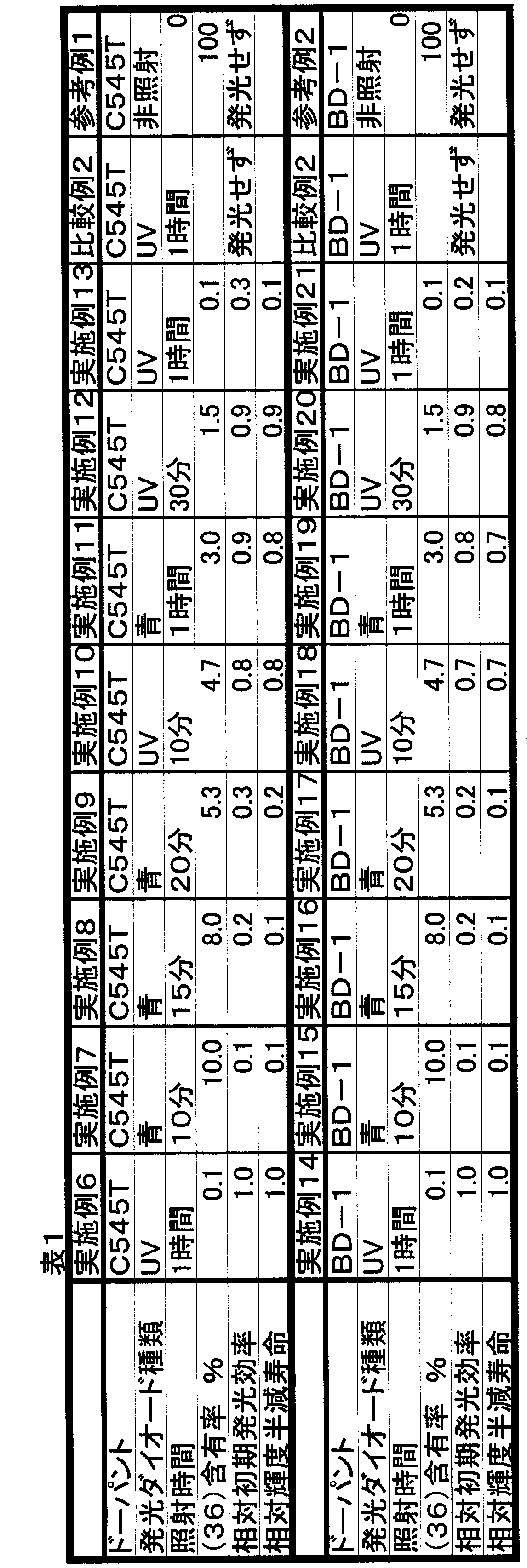
11 支持体
12 TFT
13 平坦化層
14 絶縁層
15 第一電極
16 正孔輸送層
17 発光層
18 電子輸送層
19 第二電極
Claims (13)
- 一般式(1)で表される発光素子材料前駆体。

- 一般式(1’)で表される発光素子材料前駆体。

- R1~R6の少なくとも1つが一般式(2-1)~(2-7)で表される骨格のいずれかを含む請求項1記載の発光素子材料前駆体。

X1~X6、Y1~Y4およびZ1~Z2はそれぞれ同じでも異なっていてもよく、水素、アルキル基、シクロアルキル基、複素環基、アルケニル基、シクロアルケニル基、アルキニル基、アルコキシ基、アルキルチオ基、アリールエーテル基、アリールチオエーテル基、アリール基、ヘテロアリール基、ハロゲン、シアノ基、カルボニル基、カルボキシル基、オキシカルボニル基、カルバモイル基、アミノ基、シリル基、ホスフィンオキサイド基並びに隣接置換基との間に形成される縮合環の中から選ばれる。
ただし式(2-1)においてはX1およびX2が水素となる場合を除く。式(2-2)においてはX3およびX4が水素となる場合、またはY1およびY2が水素となる場合を除く。式(2-3)においてはX5およびX6が水素となる場合、Y3およびY4が水素となる場合、又はZ1およびZ2が水素となる場合を除く。
式(2-1)においてR10~R17およびX1~X2、式(2-2)においてR20~R27、X3~X4およびY1~Y2、式(2-3)においてR30~R37、X5~X6、Y3~Y4およびZ1~Z2、式(2-4)においてR40~R49、式(2-5)においてR50~R61、式(2-6)においてR70~R81、ならびに式(2-5)においてR82~R89はそれぞれ少なくとも一つは直接結合または連結基を介して式(1)の[2,2,2]-ビシクロオクタジエン-2,3-ジオン部位との連結に用いられる。) - 一般式(3)または(4)で表される発光素子材料前駆体。


- 一般式(5)または(6)で表される発光素子材料前駆体。


- 一般式(5’)又は一般式(6’)で表される発光素子材料前駆体。

R140~R144、R160~R164はそれぞれ同じでも異なっていてもよく、水素、アルキル基、シクロアルキル基、アルケニル基、シクロアルケニル基、アルコキシ基、アルキルチオ基、アリールエーテル基、アリールチオエーテル基、アリール基、ヘテロアリール基の中から選ばれる。ただしこれら官能基の少なくとも1つはEとの結合に用いられる。
R180~R197はそれぞれ同じでも異なっていてもよく、水素、アルキル基、シクロアルキル基、複素環基、アルケニル基、シクロアルケニル基、アルキニル基、アルコキシ基、アルキルチオ基、アリールエーテル基、アリールチオエーテル基、アリール基、ヘテロアリール基、ハロゲン、シアノ基、カルボニル基、カルボキシル基、オキシカルボニル基、カルバモイル基、アミノ基、シリル基、ホスフィンオキサイド基並びに隣接置換基との間に形成される縮合環の中から選ばれ、これらのうちいずれか1つがEとの結合に用いられる) - 請求項1~6のいずれか記載の発光素子材料前駆体を含む溶液。
- 請求項7に記載の発光素子材料前駆体を含む溶液をドナー基板に塗布する工程と、塗布後に前記発光素子材料前駆体を発光素子材料へと変換させる工程と、前記ドナー基板上の発光素子材料をデバイス基板に転写する工程とを含むことを特徴とする発光素子の製造方法。
- 発光素子材料へ変換させるための手段が光照射である請求項7記載の発光素子の製造方法。
- 下部電極と発光素子材料からなる層を少なくとも1つ含む発光素子材料層と上部電極とからなる発光素子であって、前記発光素子材料からなる層が請求項1~6のいずれか記載の発光素子材料前駆体を含み、その含有量が5%未満である発光素子。
- 下記の式(7)で表される化合物からそのR171を置換する反応により式(8)で表される化合物を得る工程、得られた式(8)で表される化合物の保護基であるR177~R178を脱離させる反応により式(9)で表される化合物とする工程、式(9)で表される化合物に対して酸化反応させて式(10)で表される化合物へ変換する工程を含むビシクロ-[2,2,2]-シクロオクタジエン-2,3-ジオン誘導体の製造方法。
(R170はアリール基又はヘテロアリール基である。R171は水素、アルキル基、シクロアルキル基、複素環基、アルケニル基、シクロアルケニル基、アルキニル基、アルコキシ基、アルキルチオ基、アリールエーテル基、アリールチオエーテル基、アリール基、ヘテロアリール基、ハロゲン、シアノ基、カルボニル基、カルボキシル基、オキシカルボニル基、カルバモイル基、アミノ基、シリル基、ホスフィンオキサイド基、置換スルホニル基の中から選ばれる。R172~R176は水素、アルキル基、シクロアルキル基、アルケニル基、シクロアルケニル基、アルコキシ基、アルキルチオ基、アリールエーテル基、アリールチオエーテル基、アリール基、ヘテロアリール基およびハロゲンの中から選ばれる。R177~R178は水素、アルキル基、アルコキシ基、アリール基、アリールエーテル基の中から選ばれる。)

- R171が電子吸引性基である請求項10に記載のビシクロ-[2,2,2]-シクロオクタジエン-2,3-ジオン誘導体の製造方法。
- R170が一般式(2-1)~(2-7)で表される骨格のいずれかを含む官能基である請求項11または12記載のビシクロ-[2,2,2]-シクロオクタジエン-2,3-ジオン誘導体の製造方法。

X1~X6、Y1~Y4およびZ1~Z2はそれぞれ同じでも異なっていてもよく、水素、アルキル基、シクロアルキル基、複素環基、アルケニル基、シクロアルケニル基、アルキニル基、アルコキシ基、アルキルチオ基、アリールエーテル基、アリールチオエーテル基、アリール基、ヘテロアリール基、ハロゲン、シアノ基、カルボニル基、カルボキシル基、オキシカルボニル基、カルバモイル基、アミノ基、シリル基、ホスフィンオキサイド基並びに隣接置換基との間に形成される縮合環の中から選ばれる。
ただし式(2-1)においてはX1およびX2が水素となる場合を除く。式(2-2)においてはX3およびX4が水素となる場合、またはおよび/又はY1およびY2が水素となる場合を除く。式(2-3)においてはX5およびX6が水素となる場合、Y3およびY4が水素となる場合、又はZ1およびZ2が水素となる場合を除く。
Priority Applications (5)
| Application Number | Priority Date | Filing Date | Title |
|---|---|---|---|
| JP2010512452A JP5099220B2 (ja) | 2009-03-31 | 2010-03-29 | 発光素子材料前駆体およびその製造方法 |
| KR1020117023084A KR101239478B1 (ko) | 2009-03-31 | 2010-03-29 | 발광 소자 재료 전구체 및 그의 제조 방법 |
| CN2010800153488A CN102378750A (zh) | 2009-03-31 | 2010-03-29 | 发光元件材料前体和其制造方法 |
| US13/257,394 US20120012833A1 (en) | 2009-03-31 | 2010-03-29 | Light-emitting element material precursor and production method therefor |
| EP10758602A EP2415746A4 (en) | 2009-03-31 | 2010-03-29 | LIGHT EMITTING ELEMENT MATERIAL PRECURSOR BODY AND METHOD FOR MANUFACTURING SAME |
Applications Claiming Priority (2)
| Application Number | Priority Date | Filing Date | Title |
|---|---|---|---|
| JP2009085785 | 2009-03-31 | ||
| JP2009-085785 | 2009-03-31 |
Publications (1)
| Publication Number | Publication Date |
|---|---|
| WO2010113831A1 true WO2010113831A1 (ja) | 2010-10-07 |
Family
ID=42828121
Family Applications (1)
| Application Number | Title | Priority Date | Filing Date |
|---|---|---|---|
| PCT/JP2010/055502 WO2010113831A1 (ja) | 2009-03-31 | 2010-03-29 | 発光素子材料前駆体およびその製造方法 |
Country Status (7)
| Country | Link |
|---|---|
| US (1) | US20120012833A1 (ja) |
| EP (1) | EP2415746A4 (ja) |
| JP (1) | JP5099220B2 (ja) |
| KR (1) | KR101239478B1 (ja) |
| CN (1) | CN102378750A (ja) |
| TW (1) | TWI395731B (ja) |
| WO (1) | WO2010113831A1 (ja) |
Cited By (1)
| Publication number | Priority date | Publication date | Assignee | Title |
|---|---|---|---|---|
| WO2013047478A1 (ja) * | 2011-09-26 | 2013-04-04 | Necライティング株式会社 | 有機el照明装置 |
Families Citing this family (10)
| Publication number | Priority date | Publication date | Assignee | Title |
|---|---|---|---|---|
| US20110089412A1 (en) * | 2008-06-16 | 2011-04-21 | Shigeo Fujimori | Patterning method, production method of device using the patterning method, and device |
| US20110136282A1 (en) * | 2008-08-05 | 2011-06-09 | Toray Industries, Inc. | Method for producing device |
| US8530270B2 (en) * | 2010-04-30 | 2013-09-10 | Eastman Kodak Company | Methods of preparing semiconductive compositions and devices |
| EP3372580B1 (de) | 2011-01-25 | 2020-07-22 | Bayer CropScience Aktiengesellschaft | Verfahren zur herstellung von 1-h-pyrrolidin-2,4-dion-derivaten |
| US9000026B2 (en) | 2011-02-17 | 2015-04-07 | Bayer Intellectual Property Gmbh | Substituted 3-(biphenyl-3-yl)-8,8-difluoro-4-hydroxy-1-azaspiro[4.5]dec-3-en-2-ones for therapy |
| KR101789527B1 (ko) | 2011-03-01 | 2017-10-25 | 바이엘 인텔렉쳐 프로퍼티 게엠베하 | 2-아실옥시피롤린-4-온 |
| JP5931362B2 (ja) * | 2011-07-01 | 2016-06-08 | 日立マクセル株式会社 | コンテンツ送信装置及びコンテンツ送信方法 |
| US9741918B2 (en) | 2013-10-07 | 2017-08-22 | Hypres, Inc. | Method for increasing the integration level of superconducting electronics circuits, and a resulting circuit |
| US9190620B2 (en) * | 2014-03-01 | 2015-11-17 | Universal Display Corporation | Organic electroluminescent materials and devices |
| CN105405864B (zh) * | 2015-12-08 | 2019-05-17 | 昆山工研院新型平板显示技术中心有限公司 | 显示装置以及显示装置的封装方法 |
Citations (2)
| Publication number | Priority date | Publication date | Assignee | Title |
|---|---|---|---|---|
| JP2006339576A (ja) * | 2005-06-06 | 2006-12-14 | Konica Minolta Holdings Inc | 有機半導体膜、有機薄膜トランジスタ及びそのそれらの製造方法 |
| JP2008135198A (ja) * | 2006-11-27 | 2008-06-12 | Konica Minolta Holdings Inc | 有機エレクトロルミネッセンス素子の製造方法、有機エレクトロルミネッセンス素子、表示装置及び照明装置 |
Family Cites Families (4)
| Publication number | Priority date | Publication date | Assignee | Title |
|---|---|---|---|---|
| JP2002063988A (ja) * | 2000-08-22 | 2002-02-28 | Toray Ind Inc | 発光素子 |
| DE60213986T2 (de) * | 2001-06-01 | 2007-09-06 | Roche Diagnostics Gmbh | Neuen reagenzien in chemilumineszenz-nachweisverfahren |
| CN1531378A (zh) * | 2003-03-11 | 2004-09-22 | 胜园科技股份有限公司 | 多层高分子电激发光元件及其制造方法 |
| TWI373506B (en) * | 2004-05-21 | 2012-10-01 | Toray Industries | Light-emitting element material and light-emitting material |
-
2010
- 2010-03-29 JP JP2010512452A patent/JP5099220B2/ja not_active Expired - Fee Related
- 2010-03-29 KR KR1020117023084A patent/KR101239478B1/ko not_active IP Right Cessation
- 2010-03-29 EP EP10758602A patent/EP2415746A4/en not_active Withdrawn
- 2010-03-29 WO PCT/JP2010/055502 patent/WO2010113831A1/ja active Application Filing
- 2010-03-29 US US13/257,394 patent/US20120012833A1/en not_active Abandoned
- 2010-03-29 CN CN2010800153488A patent/CN102378750A/zh active Pending
- 2010-03-30 TW TW099109495A patent/TWI395731B/zh not_active IP Right Cessation
Patent Citations (2)
| Publication number | Priority date | Publication date | Assignee | Title |
|---|---|---|---|---|
| JP2006339576A (ja) * | 2005-06-06 | 2006-12-14 | Konica Minolta Holdings Inc | 有機半導体膜、有機薄膜トランジスタ及びそのそれらの製造方法 |
| JP2008135198A (ja) * | 2006-11-27 | 2008-06-12 | Konica Minolta Holdings Inc | 有機エレクトロルミネッセンス素子の製造方法、有機エレクトロルミネッセンス素子、表示装置及び照明装置 |
Non-Patent Citations (3)
| Title |
|---|
| C.C.LIAO ET AL.: "Chemistry of O-Benzoquinones and Masked O-Benzoquinones I.Diels-Alder Reactions of O-Benzoquinones with Dimethyl Acetylenedicarboxylate and Phenylacetylene", J.CHINESE CHEM.SOC., vol. 27, 1980, pages 87 - 95, XP008164334 * |
| CHUN-CHEN LIAO ET AL.: "Cycloaddition Reactions of 3,5-Di-t-Butyl-O-Benzoquinone and Masked 3,5-Di-t-Butyl-0-benzoquinones with Substituted Acetylenes", J.CHINESE CHEM.SOC, vol. 33, 1986, pages 73 - 82, XP008164335 * |
| See also references of EP2415746A4 * |
Cited By (2)
| Publication number | Priority date | Publication date | Assignee | Title |
|---|---|---|---|---|
| WO2013047478A1 (ja) * | 2011-09-26 | 2013-04-04 | Necライティング株式会社 | 有機el照明装置 |
| JPWO2013047478A1 (ja) * | 2011-09-26 | 2015-03-26 | Necライティング株式会社 | 有機el照明装置 |
Also Published As
| Publication number | Publication date |
|---|---|
| KR101239478B1 (ko) | 2013-03-06 |
| TW201038524A (en) | 2010-11-01 |
| CN102378750A (zh) | 2012-03-14 |
| US20120012833A1 (en) | 2012-01-19 |
| JPWO2010113831A1 (ja) | 2012-10-11 |
| EP2415746A4 (en) | 2012-10-31 |
| KR20120022750A (ko) | 2012-03-12 |
| EP2415746A1 (en) | 2012-02-08 |
| TWI395731B (zh) | 2013-05-11 |
| JP5099220B2 (ja) | 2012-12-19 |
Similar Documents
| Publication | Publication Date | Title |
|---|---|---|
| JP5099220B2 (ja) | 発光素子材料前駆体およびその製造方法 | |
| JP5177145B2 (ja) | デバイスの製造方法 | |
| TW200927878A (en) | New compound and organic light emitting device using the same | |
| JP5773638B2 (ja) | 縮合多環化合物及びこれを用いた有機発光素子 | |
| JP2021038206A (ja) | 多環芳香族化合物 | |
| JP2013093432A (ja) | 有機エレクトロルミネッセンス素子用材料、有機エレクトロルミネッセンス素子、表示装置及び照明装置 | |
| CN115867558A (zh) | 多环芳香族化合物 | |
| CN113429385B (zh) | 噻吨衍生物及其应用 | |
| WO2011074428A1 (ja) | 発光素子用材料の製造方法、発光素子用材料前駆体および発光素子の製造方法 | |
| WO2011068083A1 (ja) | 有機el素子および有機el素子の製造方法 | |
| JP7376892B2 (ja) | 多環芳香族化合物 | |
| CN112110949A (zh) | 多环芳香族化合物、有机器件用材料、有机电致发光元件、显示装置及照明装置 | |
| CN113429348A (zh) | 一种蒽并咪唑衍生物、有机电致发光材料及消费型产品 | |
| WO2013146630A1 (ja) | 有機デバイス材料前駆体およびその製造方法ならびにこれを用いた発光素子およびその製造方法 | |
| JP2023148087A (ja) | 金属錯体 | |
| WO2013146631A1 (ja) | 有機デバイス材料前駆体およびその製造方法ならびにこれを用いた発光素子およびその製造方法 | |
| JP2022017207A (ja) | 多環芳香族化合物 | |
| JP2024007338A (ja) | 多環芳香族化合物 | |
| JP2021113160A (ja) | 多環芳香族化合物 | |
| JP2022032441A (ja) | 多環芳香族化合物 | |
| JP2023180606A (ja) | 多環芳香族化合物 | |
| JP2023549688A (ja) | 新規な化合物、それを含むコーティング組成物、それを用いた有機発光素子、およびその製造方法 | |
| CN116249423A (zh) | 多环芳香族化合物、有机电场发光元件、显示装置及照明装置 | |
| CN116997557A (zh) | 多环芳香族化合物及有机电致发光元件 |
Legal Events
| Date | Code | Title | Description |
|---|---|---|---|
| WWE | Wipo information: entry into national phase |
Ref document number: 201080015348.8 Country of ref document: CN |
|
| WWE | Wipo information: entry into national phase |
Ref document number: 2010512452 Country of ref document: JP |
|
| 121 | Ep: the epo has been informed by wipo that ep was designated in this application |
Ref document number: 10758602 Country of ref document: EP Kind code of ref document: A1 |
|
| WWE | Wipo information: entry into national phase |
Ref document number: 2010758602 Country of ref document: EP |
|
| WWE | Wipo information: entry into national phase |
Ref document number: 13257394 Country of ref document: US |
|
| ENP | Entry into the national phase |
Ref document number: 20117023084 Country of ref document: KR Kind code of ref document: A |
|
| NENP | Non-entry into the national phase |
Ref country code: DE |
|
| WWE | Wipo information: entry into national phase |
Ref document number: 7119/CHENP/2011 Country of ref document: IN |