WO2010109558A1 - Tft基板及びこれを用いた液晶表示装置 - Google Patents
Tft基板及びこれを用いた液晶表示装置 Download PDFInfo
- Publication number
- WO2010109558A1 WO2010109558A1 PCT/JP2009/005883 JP2009005883W WO2010109558A1 WO 2010109558 A1 WO2010109558 A1 WO 2010109558A1 JP 2009005883 W JP2009005883 W JP 2009005883W WO 2010109558 A1 WO2010109558 A1 WO 2010109558A1
- Authority
- WO
- WIPO (PCT)
- Prior art keywords
- bus line
- pixel
- subpixel
- sub
- auxiliary
- Prior art date
Links
Images


Classifications
-
- G—PHYSICS
- G02—OPTICS
- G02F—OPTICAL DEVICES OR ARRANGEMENTS FOR THE CONTROL OF LIGHT BY MODIFICATION OF THE OPTICAL PROPERTIES OF THE MEDIA OF THE ELEMENTS INVOLVED THEREIN; NON-LINEAR OPTICS; FREQUENCY-CHANGING OF LIGHT; OPTICAL LOGIC ELEMENTS; OPTICAL ANALOGUE/DIGITAL CONVERTERS
- G02F1/00—Devices or arrangements for the control of the intensity, colour, phase, polarisation or direction of light arriving from an independent light source, e.g. switching, gating or modulating; Non-linear optics
- G02F1/01—Devices or arrangements for the control of the intensity, colour, phase, polarisation or direction of light arriving from an independent light source, e.g. switching, gating or modulating; Non-linear optics for the control of the intensity, phase, polarisation or colour
- G02F1/13—Devices or arrangements for the control of the intensity, colour, phase, polarisation or direction of light arriving from an independent light source, e.g. switching, gating or modulating; Non-linear optics for the control of the intensity, phase, polarisation or colour based on liquid crystals, e.g. single liquid crystal display cells
- G02F1/133—Constructional arrangements; Operation of liquid crystal cells; Circuit arrangements
- G02F1/136—Liquid crystal cells structurally associated with a semi-conducting layer or substrate, e.g. cells forming part of an integrated circuit
- G02F1/1362—Active matrix addressed cells
- G02F1/136213—Storage capacitors associated with the pixel electrode
-
- G—PHYSICS
- G02—OPTICS
- G02F—OPTICAL DEVICES OR ARRANGEMENTS FOR THE CONTROL OF LIGHT BY MODIFICATION OF THE OPTICAL PROPERTIES OF THE MEDIA OF THE ELEMENTS INVOLVED THEREIN; NON-LINEAR OPTICS; FREQUENCY-CHANGING OF LIGHT; OPTICAL LOGIC ELEMENTS; OPTICAL ANALOGUE/DIGITAL CONVERTERS
- G02F1/00—Devices or arrangements for the control of the intensity, colour, phase, polarisation or direction of light arriving from an independent light source, e.g. switching, gating or modulating; Non-linear optics
- G02F1/01—Devices or arrangements for the control of the intensity, colour, phase, polarisation or direction of light arriving from an independent light source, e.g. switching, gating or modulating; Non-linear optics for the control of the intensity, phase, polarisation or colour
- G02F1/13—Devices or arrangements for the control of the intensity, colour, phase, polarisation or direction of light arriving from an independent light source, e.g. switching, gating or modulating; Non-linear optics for the control of the intensity, phase, polarisation or colour based on liquid crystals, e.g. single liquid crystal display cells
- G02F1/133—Constructional arrangements; Operation of liquid crystal cells; Circuit arrangements
- G02F1/1333—Constructional arrangements; Manufacturing methods
- G02F1/1343—Electrodes
- G02F1/134309—Electrodes characterised by their geometrical arrangement
- G02F1/134336—Matrix
-
- G—PHYSICS
- G02—OPTICS
- G02F—OPTICAL DEVICES OR ARRANGEMENTS FOR THE CONTROL OF LIGHT BY MODIFICATION OF THE OPTICAL PROPERTIES OF THE MEDIA OF THE ELEMENTS INVOLVED THEREIN; NON-LINEAR OPTICS; FREQUENCY-CHANGING OF LIGHT; OPTICAL LOGIC ELEMENTS; OPTICAL ANALOGUE/DIGITAL CONVERTERS
- G02F1/00—Devices or arrangements for the control of the intensity, colour, phase, polarisation or direction of light arriving from an independent light source, e.g. switching, gating or modulating; Non-linear optics
- G02F1/01—Devices or arrangements for the control of the intensity, colour, phase, polarisation or direction of light arriving from an independent light source, e.g. switching, gating or modulating; Non-linear optics for the control of the intensity, phase, polarisation or colour
- G02F1/13—Devices or arrangements for the control of the intensity, colour, phase, polarisation or direction of light arriving from an independent light source, e.g. switching, gating or modulating; Non-linear optics for the control of the intensity, phase, polarisation or colour based on liquid crystals, e.g. single liquid crystal display cells
- G02F1/133—Constructional arrangements; Operation of liquid crystal cells; Circuit arrangements
- G02F1/136—Liquid crystal cells structurally associated with a semi-conducting layer or substrate, e.g. cells forming part of an integrated circuit
- G02F1/1362—Active matrix addressed cells
- G02F1/13624—Active matrix addressed cells having more than one switching element per pixel
-
- G—PHYSICS
- G09—EDUCATION; CRYPTOGRAPHY; DISPLAY; ADVERTISING; SEALS
- G09G—ARRANGEMENTS OR CIRCUITS FOR CONTROL OF INDICATING DEVICES USING STATIC MEANS TO PRESENT VARIABLE INFORMATION
- G09G3/00—Control arrangements or circuits, of interest only in connection with visual indicators other than cathode-ray tubes
- G09G3/20—Control arrangements or circuits, of interest only in connection with visual indicators other than cathode-ray tubes for presentation of an assembly of a number of characters, e.g. a page, by composing the assembly by combination of individual elements arranged in a matrix no fixed position being assigned to or needed to be assigned to the individual characters or partial characters
- G09G3/34—Control arrangements or circuits, of interest only in connection with visual indicators other than cathode-ray tubes for presentation of an assembly of a number of characters, e.g. a page, by composing the assembly by combination of individual elements arranged in a matrix no fixed position being assigned to or needed to be assigned to the individual characters or partial characters by control of light from an independent source
- G09G3/36—Control arrangements or circuits, of interest only in connection with visual indicators other than cathode-ray tubes for presentation of an assembly of a number of characters, e.g. a page, by composing the assembly by combination of individual elements arranged in a matrix no fixed position being assigned to or needed to be assigned to the individual characters or partial characters by control of light from an independent source using liquid crystals
- G09G3/3611—Control of matrices with row and column drivers
- G09G3/3648—Control of matrices with row and column drivers using an active matrix
- G09G3/3655—Details of drivers for counter electrodes, e.g. common electrodes for pixel capacitors or supplementary storage capacitors
-
- G—PHYSICS
- G02—OPTICS
- G02F—OPTICAL DEVICES OR ARRANGEMENTS FOR THE CONTROL OF LIGHT BY MODIFICATION OF THE OPTICAL PROPERTIES OF THE MEDIA OF THE ELEMENTS INVOLVED THEREIN; NON-LINEAR OPTICS; FREQUENCY-CHANGING OF LIGHT; OPTICAL LOGIC ELEMENTS; OPTICAL ANALOGUE/DIGITAL CONVERTERS
- G02F1/00—Devices or arrangements for the control of the intensity, colour, phase, polarisation or direction of light arriving from an independent light source, e.g. switching, gating or modulating; Non-linear optics
- G02F1/01—Devices or arrangements for the control of the intensity, colour, phase, polarisation or direction of light arriving from an independent light source, e.g. switching, gating or modulating; Non-linear optics for the control of the intensity, phase, polarisation or colour
- G02F1/13—Devices or arrangements for the control of the intensity, colour, phase, polarisation or direction of light arriving from an independent light source, e.g. switching, gating or modulating; Non-linear optics for the control of the intensity, phase, polarisation or colour based on liquid crystals, e.g. single liquid crystal display cells
- G02F1/133—Constructional arrangements; Operation of liquid crystal cells; Circuit arrangements
- G02F1/1333—Constructional arrangements; Manufacturing methods
- G02F1/1343—Electrodes
- G02F1/134309—Electrodes characterised by their geometrical arrangement
- G02F1/134345—Subdivided pixels, e.g. for grey scale or redundancy
-
- G—PHYSICS
- G09—EDUCATION; CRYPTOGRAPHY; DISPLAY; ADVERTISING; SEALS
- G09G—ARRANGEMENTS OR CIRCUITS FOR CONTROL OF INDICATING DEVICES USING STATIC MEANS TO PRESENT VARIABLE INFORMATION
- G09G2300/00—Aspects of the constitution of display devices
- G09G2300/04—Structural and physical details of display devices
- G09G2300/0439—Pixel structures
- G09G2300/0443—Pixel structures with several sub-pixels for the same colour in a pixel, not specifically used to display gradations
- G09G2300/0447—Pixel structures with several sub-pixels for the same colour in a pixel, not specifically used to display gradations for multi-domain technique to improve the viewing angle in a liquid crystal display, such as multi-vertical alignment [MVA]
-
- G—PHYSICS
- G09—EDUCATION; CRYPTOGRAPHY; DISPLAY; ADVERTISING; SEALS
- G09G—ARRANGEMENTS OR CIRCUITS FOR CONTROL OF INDICATING DEVICES USING STATIC MEANS TO PRESENT VARIABLE INFORMATION
- G09G2320/00—Control of display operating conditions
- G09G2320/02—Improving the quality of display appearance
- G09G2320/028—Improving the quality of display appearance by changing the viewing angle properties, e.g. widening the viewing angle, adapting the viewing angle to the view direction
Definitions
- the present invention relates to an active matrix TFT substrate using thin film transistors and a liquid crystal display device using the same.
- multi-pixel drive type liquid crystal display device as a liquid crystal display device with improved viewing angle dependency of the ⁇ characteristic.
- one pixel is composed of two or more sub-pixels having different luminances, thereby improving the viewing angle dependency of viewing angle characteristics, that is, ⁇ characteristics (see, for example, Patent Document 1).
- FIG. 9 shows a configuration example of a pixel included in a conventional multi-pixel driving type liquid crystal display device.
- one pixel P 1 is divided two to the sub-pixels SP 1, SP 2.
- the subpixel SP 1 includes a thin film transistor (hereinafter referred to as “TFT”) 51, an auxiliary capacitor 52, and a subpixel electrode 53.
- the subpixel SP 2 includes a TFT 61, an auxiliary capacitor 62, and a subpixel electrode 63.
- each gate of - gate electrode is connected to the gate bus lines G 1, each of the source electrodes are connected to the source bus line S 1.
- the auxiliary capacitor 52 is formed between the sub-pixel electrode 53 and the auxiliary capacitor bus line Cs 1 .
- Auxiliary capacitance 62 is formed between the subpixel electrode 63 and the auxiliary capacitor bus line Cs 2.
- the auxiliary capacitance bus line Cs 1 and the gate bus line G 1 are arranged to be parallel to each other so as to sandwich the sub-pixel SP 1 .
- the auxiliary capacitance bus line Cs 2 and the gate bus line G 1 are arranged to be parallel to each other so as to sandwich the sub-pixel SP 2 .
- the auxiliary capacitor bus line Cs 1 pixel P 1 an auxiliary for forming a storage capacitor subpixel of another pixel adjacent to the pixel P 1 across the auxiliary capacitor bus line Cs 1 (not shown) having Also serves as a capacity bus line.
- the auxiliary capacitor bus line Cs 2 of pixels P 1 is, for forming a storage capacitor subpixel of another pixel adjacent to the pixel P 1 across the auxiliary capacitor bus line Cs 2 (not shown) having Also serves as an auxiliary capacity bus line.
- Cs 1 and Cs 2 may be collectively referred to as “Cs”.
- the storage capacitor bus lines Cs alternately arranged in the active area AA as the display area are connected to the Cs trunk wiring bb arranged in the area adjacent to the active area AA.
- a plurality of Cs trunk lines bb constitute one set of Cs trunk line group BB1 and Cs trunk line group BB2.
- the Cs trunk line group BB1 is provided in a region adjacent to one end side of the active area AA, which is a predetermined side in one direction in which the storage capacitor bus line Cs extends with respect to the active area AA.
- the Cs trunk line group BB2 is provided in a region adjacent to the other end side of the active area AA, which is a predetermined side in the other direction in which the auxiliary capacitance bus line Cs extends with respect to the active area AA.
- auxiliary capacity bus line Cs is connected to the Cs trunk line bb constituting the Cs trunk line group BB1.
- the Cs trunk line group BB1 and the Cs trunk line group BB2 are provided, one end of the auxiliary capacitance bus line Cs is connected to the Cs trunk line bb constituting the Cs trunk line group BB1, The other end of the auxiliary capacitance bus line Cs is connected to the Cs trunk wiring bb that constitutes the Cs trunk wiring group BB2.
- Cs trunk wiring bb is a direction perpendicular to the extending direction of the auxiliary capacitor bus line Cs, i.e. extends in the direction of extension of the source bus line S 1 in FIG.
- a Cs trunk line group BB1 composed of 12 Cs trunk lines bb and a Cs trunk line group BB2 composed of 12 Cs trunk lines bb are provided.
- Each auxiliary capacitance bus line Cs is connected to one Cs trunk line bb of each of the Cs trunk line groups BB1 and BB2.
- Twelve storage capacitor bus lines Cs arranged in succession are connected to different Cs trunk lines bb in the Cs trunk line groups BB1 and BB2.
- the 12 auxiliary capacitor bus lines Cs arranged in succession are connected to different Cs trunk lines bb in the Cs trunk line group BB1. Will be.
- the auxiliary capacitance voltage Vcs is supplied to the auxiliary capacitance bus line Cs 1 and the auxiliary capacitance bus line Cs 2 via the Cs trunk line bb.
- Different auxiliary capacitance voltages Vcs are applied to the different Cs trunk lines bb of the Cs trunk line groups BB1 and BB2. For this reason, different auxiliary capacitance voltages Vcs corresponding to the number of Cs trunk lines bb are supplied from the Cs driver (not shown) to each of the Cs trunk lines BB1 and BB2.
- each of the Cs trunk wiring groups BB1 and BB2 connected to the same auxiliary capacitance bus line Cs.
- the same auxiliary capacitance voltage Vcs is applied to the Cs trunk wiring bb.
- the auxiliary capacitance voltage Vcs is supplied from both sides of the active area AA. For this reason, even if the liquid crystal screen has a large size, the waveform of the auxiliary capacitance voltage Vcs is suppressed between different locations of the active area AA in the same auxiliary capacitance bus line Cs due to the wiring delay of the auxiliary capacitance voltage Vcs. can do.
- the storage capacitor bus line corresponding to the auxiliary capacitor bus line Cs shown in FIG. The impedance of the line can be made extremely small. For this reason, the time constant of the storage capacitor bus line can be reduced, so that the liquid crystal display device can be increased in size and definition without lowering the display quality.
- the auxiliary capacitance wiring unit corresponding to the auxiliary capacitance bus line Cs shown in FIG. Can be lowered. Furthermore, even if a disconnection occurs in the auxiliary capacity wiring unit, the entire auxiliary capacity wiring is formed in a mesh shape, so that the adverse effects of the disconnection can be minimized.
- an object of the present invention is to provide a TFT substrate that can accurately hold the pixel potentials of a plurality of pixels arranged on the TFT substrate, and a liquid crystal display device using the TFT substrate.
- a TFT substrate includes an active matrix in which a plurality of pixels are arranged in a matrix, which includes a first subpixel and a second subpixel adjacent to the first subpixel.
- a first and second gate bus lines extending along adjacent directions in which the first subpixel and the second subpixel are adjacent to each other, and the first and second gate bus lines.
- First and second auxiliary capacitance bus lines that are configured of the same wiring layer as the gate bus line and extend along the adjacent direction, and the same wiring layer as the first and second gate bus lines
- a third auxiliary capacitance bus line that is adjacent to the first subpixel and forms an auxiliary capacitance of the first subpixel between the first subpixel and the subpixel electrode of the first subpixel.
- the first and second gate bus slats A fourth sub-pixel is formed in the same wiring layer as that of the second sub-pixel, is adjacent to the second sub-pixel, and forms a storage capacitor of the second sub-pixel between the second sub-pixel and the sub-pixel electrode of the second sub-pixel. And the first auxiliary capacitor bus line and the first subpixel are arranged so as to sandwich the first gate bus line, and the second auxiliary capacitor bus line and the first subpixel bus line are arranged.
- the two sub-pixels are arranged so as to sandwich the second gate bus line, and different voltages are applied to the first auxiliary capacitor bus line and the second auxiliary capacitor bus line,
- a first connection wiring portion configured by a wiring layer different from the first and second gate bus lines, which connects the first auxiliary capacitance bus line and the third auxiliary capacitance bus line;
- the second auxiliary capacity bus Connecting between the in-fourth auxiliary capacitor bus lines further includes a second connection wiring part that is composed of a wiring layer different from the first and second gate bus line.
- the first subpixel forms an auxiliary capacitance with the third auxiliary capacitance bus line close to itself.
- the third auxiliary capacitance bus line is connected to the first auxiliary capacitance bus line via a first connection wiring portion configured from a different wiring layer from the first and second gate bus lines.
- the second subpixel forms an auxiliary capacitance with the fourth auxiliary capacitance bus line close to itself.
- the fourth auxiliary capacitance bus line is connected to the second auxiliary capacitance bus line via a second connection wiring portion configured from a different wiring layer from the first and second gate bus lines. Yes.
- the first auxiliary capacitor bus line and the third auxiliary capacitor bus line can be formed in a mesh pattern on the TFT substrate. Further, the second auxiliary capacitor bus line and the fourth auxiliary capacitor bus line can be formed in a mesh pattern on the TFT substrate.
- the same auxiliary capacitance voltage can be uniformly supplied to each pixel on the TFT substrate using the first auxiliary capacitance bus line and the third auxiliary capacitance bus line, and the second auxiliary capacitance bus line can be supplied.
- the same auxiliary capacitance voltage different from the auxiliary capacitance voltage applied to the first auxiliary capacitance bus line can be uniformly supplied to each pixel on the TFT substrate. By doing so, the pixel potential of each pixel in multi-image driving using two different voltages can be held with high accuracy.
- a liquid crystal display device includes the above-described TFT substrate and a control circuit for controlling an image display process for displaying an image using the TFT substrate.
- the first sub-pixel forms an auxiliary capacitor with the second auxiliary capacitor bus line adjacent to the first sub-pixel.
- the second auxiliary capacitance bus line is connected to the first auxiliary capacitance bus line via a connection wiring portion formed of a wiring layer different from the gate bus line.
- the first auxiliary capacitor bus line and the second auxiliary capacitor bus line can be formed in a mesh pattern on the TFT substrate. Therefore, since the same auxiliary capacitance voltage can be uniformly supplied to each pixel on the TFT substrate using the first auxiliary capacitance bus line and the second auxiliary capacitance bus line, the pixel potential of each pixel is accurately determined. Can hold well.
- the TFT substrate of the present invention includes the first and second gate bus lines extending along the adjacent direction in which the first subpixel and the second subpixel are adjacent, and the first subpixel.
- the first and second auxiliary bus lines which are formed of the same wiring layer as the second gate bus lines and extend along the adjacent direction, and the first and second gate bus lines.
- a third auxiliary that is formed of the same wiring layer and is adjacent to the first subpixel and forms an auxiliary capacitance of the first subpixel between the first subpixel and the subpixel electrode of the first subpixel.
- the capacitor bus line is composed of the same wiring layer as the first and second gate bus lines, and is close to the second subpixel and between the subpixel electrode of the second subpixel.
- a fourth auxiliary capacitance busler forming an auxiliary capacitance of the second subpixel;
- the first auxiliary capacitor bus line and the first subpixel are arranged so as to sandwich the first gate bus line, and the second auxiliary capacitor busline and the second subpixel Are arranged so as to sandwich the second gate bus line, and different voltages are applied to the first auxiliary capacitor bus line and the second auxiliary capacitor bus line, respectively.
- a first connection wiring portion configured by a wiring layer different from the first and second gate bus lines, which connects between the auxiliary capacitance bus line and the third auxiliary capacitance bus line; and the second And a second connection wiring portion formed of a wiring layer different from the first and second gate bus lines, which connects between the auxiliary capacitance bus line and the fourth auxiliary capacitance bus line. Is what .
- FIG. 3 is a circuit diagram showing an arrangement configuration of a plurality of pixels arranged on an active area of the liquid crystal display device according to Embodiment 1 of the present invention. It is sectional drawing which looked at the A section of FIG. 1 from the II direction. It is a block diagram which shows the structure of the liquid crystal display device in Embodiment 1 of this invention. It is a circuit diagram which shows the arrangement configuration of the some pixel arrange
- FIG. 3 is a block diagram showing the configuration of the liquid crystal display device 1 according to Embodiment 1 of the present invention.
- the liquid crystal display device 1 according to the present embodiment includes an active matrix display unit (TFT substrate) 2, a source driver 3, a gate driver (GD) 4, a display control circuit 5, Cs control circuits 6 and 7 are provided.
- TFT substrate active matrix display unit
- GD gate driver
- Cs control circuits 6 and 7 are provided.
- These components may be mounted on a single panel, or part or all of the source driver 3, the gate driver 4, the display control circuit 5, and the Cs control circuits 6 and 7 are flexible.
- the configuration may be such that it is mounted on an external substrate such as a printed circuit board and connected to a panel including the display unit 2.
- the display unit 2, the source driver 3, the gate driver 4, the display control circuit 5, and the Cs control circuits 6 and 7 can be arbitrarily arranged.
- the display unit 2 includes an active area AA in which a plurality of pixels are arranged in a matrix, a plurality of gate bus lines, a plurality of source bus lines, a plurality of auxiliary capacitance bus lines, and two Cs trunk lines.
- Pixel P 2 is composed of sub-pixels SP 21 and the sub-pixel SP 22.
- a gate electrode of each TFT (not shown) included in the subpixel SP 21 and the subpixel SP 22 is connected to the gate bus line G 3 , and each source electrode is connected to the source bus line S 1 . .
- the gate bus line and the source bus light are arranged so as to cross each other.
- Cs main line group BB 1 is provided in a region adjacent to the active area AA, one area adjacent to the side of the direction in which the auxiliary capacitor bus line extends.
- Cs trunk line group BB 2 is out of the area adjacent to the active area AA, provided in a region adjacent to the other side of the direction of extension of the auxiliary capacitor bus line. Then, the auxiliary capacitor bus line is connected to each of the Cs trunk wiring group BB 1 and Cs main line group BB 2.
- the display control circuit 5 controls the source driver 3, the gate driver 4, the Cs control circuit 6, and the Cs control circuit 7.
- the display control circuit 5 receives a digital video signal Dv representing an image to be displayed, a horizontal synchronizing signal HSY and a vertical synchronizing signal VSY corresponding to the digital video signal Dv, and a display operation from an external signal source such as a tuner. And a control signal Dc for controlling.
- the display control circuit 5 generates and outputs a plurality of signals for displaying the image represented by the digital video signal Dv on the display unit 2 using the received signals Dv, HSY, VSY, and Dc. .
- the display control circuit 5 includes a data start pulse signal SSP, a data clock signal SCK, a latch strobe signal LS, and a digital image signal DA (video signal Dv) representing an image to be displayed as the plurality of signals. ), A gate start pulse signal GSP, a gate clock signal GCK, and a gate driver output control signal (scanning signal output control signal) GOE.
- the display control circuit 5 adjusts the timing of the video signal Dv as necessary in the internal memory, and then outputs it as a digital image signal DA, corresponding to each pixel of the image represented by the digital image signal DA.
- a data clock signal SCK is generated as a signal composed of pulses to be transmitted.
- the display control circuit 5 generates the data start pulse signal SSP as a signal that becomes a high level (H level) for a predetermined period every horizontal scanning period based on the horizontal synchronization signal HSY, and 1 frame based on the vertical synchronization signal VSY.
- a gate start pulse signal GSP is generated as a signal that becomes H level for a predetermined period every period (one vertical scanning period).
- the display control circuit 5 generates a gate clock signal GCK based on the horizontal synchronization signal HSY, and generates a latch strobe signal LS and a gate driver output control signal GOE based on the horizontal synchronization signal HSY and the control signal Dc.
- the digital image signal DA the latch strobe signal LS, the signal POL for controlling the polarity of the signal potential (data signal potential), the data start pulse signal SSP, and the data
- the clock signal SCK is input to the source driver 3, and the gate start pulse signal GSP, the gate clock signal GCK, and the gate driver output control signal GOE are input to the gate driver 4.
- the source driver 3 sequentially generates a data signal for each horizontal scanning period based on the digital image signal DA, the data clock signal SCK, the latch strobe signal LS, the data start pulse signal SSP, and the polarity inversion signal POL.
- a data signal is output to the source bus line.
- These data signals are analog potentials corresponding to the pixel values of the pixels connected to the scanning signal lines of the image represented by the digital image signal DA.
- the gate driver 4 generates a scanning signal based on the gate start pulse signal GSP, the gate clock signal GCK, and the gate driver output control signal GOE, and outputs them to the gate bus line, whereby the gate bus line is selected. Driven.
- the source bus line and the gate bus line of the display unit 2 are driven by the source driver 3 and the gate driver 4, so that the sub bus is connected from the source bus line through the TFT connected to the selected gate bus line.
- a signal potential is written to the pixel electrode.
- a voltage corresponding to the digital image signal DA is applied to the liquid crystal layer of the sub-pixel included in each pixel, and the amount of light transmitted from the backlight is controlled by the voltage application, and the image indicated by the digital video signal Dv is applied to the pixel. Is displayed.
- the Cs control circuits 6 and 7 are based on the gate start pulse signal GSP and the gate clock signal GCK output from the display control circuit 5, and the phase and period of the auxiliary capacitance voltage Vcs for controlling the potential of the auxiliary capacitance bus line.
- Is a circuit for controlling Cs control circuit 6 outputs an auxiliary capacitance voltage Vcs to Cs main line group BB 1
- Cs control circuit 7 outputs an auxiliary capacitance voltage Vcs to Cs main line group BB 2.
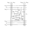
- FIG. 1 is a circuit diagram showing an arrangement configuration of a plurality of pixels arranged on the active area AA of the liquid crystal display device 1 shown in FIG.
- the pixel P 1 and the pixel P 2 are disposed.
- the pixel P 1 includes a sub-pixel SP 11 (first sub-pixel) and a sub-pixel SP 12 (second sub-pixel), and the pixel P 2 is a sub-pixel SP 21 (first sub-pixel). And the sub-pixel SP 22 (second sub-pixel).
- the subpixel SP 11 includes a TFT (thin film transistor) 11, an auxiliary capacitor 12, and a subpixel electrode 13.
- the subpixel SP 12 includes a TFT 14, an auxiliary capacitor 15, and a subpixel electrode 16.
- the gate electrode of the TFT 11 of the sub-pixel SP 11 is connected to the gate bus line G 2 (second gate bus line), and its source electrode is connected to the source bus line S 1 .
- the TFT14 subpixels SP 12 gate - gate electrode is connected to the gate bus line G 2, its source electrode is connected to the source bus line S 1.
- the auxiliary capacitance 12 of the subpixel SP 11 is formed between the subpixel electrode 13 and the auxiliary capacitance bus line Cs XH1 (third auxiliary capacitance bus line).
- the auxiliary capacitor 15 of the sub-pixel SP 12 is formed between the sub-pixel electrode 16 and the auxiliary capacitor bus line Cs XL2 (fourth auxiliary capacitor bus line).
- the sub-pixel SP 11 and the sub-pixel SP 12 both are adjacent so as to be sandwiched between the auxiliary capacitor bus line Cs XH1 and the auxiliary capacitor bus line Cs XL2. Further, the sub-pixel SP 11, while being disposed close to the auxiliary capacitor bus line Cs XH1, subpixels SP 12 is located proximate to the auxiliary capacitor bus line Cs XL2.
- the subpixel SP 21 includes a TFT 21, an auxiliary capacitor 22, and a subpixel electrode 23.
- the subpixel SP 22 includes a TFT 24, an auxiliary capacitor 25, and a subpixel electrode 26.
- the gate electrode of the TFT 21 of the sub-pixel SP 21 is connected to the gate bus line G 3 (first gate bus line), and its source electrode is connected to the source bus line S 1 .
- the TFT24 subpixels SP 22 gate - gate electrode is connected to the gate bus line G 3, its source electrode is connected to the source bus line S 1.
- the auxiliary capacitor 22 of the subpixel SP 21 is formed between the subpixel electrode 23 and the auxiliary capacitor bus line Cs XH1 .
- the auxiliary capacitor 25 of the subpixel SP 22 is formed between the subpixel electrode 26 and the auxiliary capacitor bus line Cs XL2 .
- the sub-pixel SP 21 and the sub-pixel SP 22 both are adjacent so as to be sandwiched between the auxiliary capacitor bus line Cs XH1 and the auxiliary capacitor bus line Cs XL2. Further, the sub-pixel SP 11, while being disposed close to the auxiliary capacitor bus line Cs XH1, subpixels SP 12 is disposed close to the auxiliary capacitor bus line Cs XL2.
- Auxiliary capacitor bus line Cs XH1 and Cs XL2, and the auxiliary capacitor bus line Cs XH2 adjacent to the auxiliary capacitor bus line Cs XL1 and the auxiliary capacitor bus line Cs XL2 close to the auxiliary capacitor bus line Cs XH1, the source bus line S 1 are arranged in parallel with each other.
- auxiliary capacity bus lines Cs YH1 , Cs YH2 , Cs YH3 (first auxiliary capacity bus line) and the auxiliary capacity bus lines Cs YL1 , Cs YL2 , Cs YL3 (second auxiliary capacity bus line) are gate buses. are arranged so as to be parallel to the line G 1, G 2 and G 3.
- the gate bus lines G 1 , G 2 and G 3 are arranged so as to be parallel to each other.
- the gate bus lines G 1 , G 2, and G 3 extend along the direction in which the subpixel SP 11 and the subpixel SP 12 are adjacent to each other and the direction in which the subpixel SP 21 and the subpixel SP 22 are adjacent to each other.
- the auxiliary capacitance bus lines Cs YH1 , Cs YH2 , CsYH3, CsYL1, Cs YL2 , and Cs YL3 the subpixel SP 11 and the subpixel SP 12 are adjacent to each other, and the subpixel SP 21 and the subpixel SP 22 And extend along adjacent directions.
- the auxiliary capacity bus line Cs XL1 is connected to each of the auxiliary capacity bus lines Cs YL1 , Cs YL2, and Cs YL3 .
- the auxiliary capacitance bus line Cs XH1 is connected to each of the auxiliary capacitance bus lines Cs YH1 , Cs YH2, and Cs YH3 .
- Auxiliary capacitor bus line Cs XL2 is connected with each of the auxiliary capacitor bus line Cs YL1, Cs YL2 and Cs YL3.
- the auxiliary capacitance bus line Cs XH2 is connected to each of the auxiliary capacitance bus lines Cs YH1 , Cs YH2, and Cs YH3 .
- auxiliary capacitor bus line is connected to each of the auxiliary capacitor bus line Cs XL1, Cs XL2, Cs YL1 , Cs YL2 and Cs YL3, the same auxiliary capacitance voltage Vcs is applied It will be.
- the same auxiliary capacitance voltage Vcs is also applied to each of the auxiliary capacitance bus lines Cs XH1 , Cs XH2 , Cs YH1 , Cs YH2 and Cs YH3 . That is, these auxiliary capacity bus lines are arranged in a mesh pattern on the active area AA.
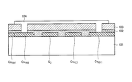
- FIG. 2 is a cross-sectional view of portion A of FIG. 1 as viewed from the II direction.
- description will be made with reference to FIGS. 1 and 2.
- the auxiliary capacitor bus line Cs XL1, Cs XL2, Cs YL1 , Cs YL2, Cs YL3, Cs XH1, Cs XH2, Cs YH1, and Cs YH2 and Cs YH3, the gate bus lines G 1, G 2 and G 3 Is generally composed of the same wiring layer.
- the auxiliary on the substrate 101 capacitor bus line Cs YL3, Cs XH1, Cs YH3 , and a gate bus line G 3 is disposed. And these auxiliary capacitor bus line Cs YL3, Cs XH1, Cs YH3 , and, on the top of the gate bus line G 3 are arranged interlayer insulating film 102 and the protective layer 103.
- Openings are provided in the interlayer insulating film 102 and the protective film 103 on the auxiliary capacitance bus line Cs XH1 .
- the interlayer insulating film 102 and the protective film 103 on the auxiliary capacitance bus line Cs YH3 are also provided with openings.
- connection structure between the auxiliary capacity bus lines Cs XH1 and Cs YH3 in the A part of FIG. 1 has been described as an example.
- the gate connection structure between the bus lines G 1 to jump over manner connected auxiliary capacitor bus line Cs YL1 and a Cs XL1 the gate bus line G 2 auxiliary capacitor is connected way jump over the bus line Cs YL2 connecting the connection structure, the connection structure between the auxiliary capacitor bus line Cs YL3 and Cs XL1 connected so as to jump over the gate bus line G 3, so as to jump over the gate bus lines G 1 between the Cs XL1 and connection structure between the connection structure, the auxiliary capacitor bus line Cs YH2 and Cs XH1 connected so as to jump over the gate bus line G 2 between the auxiliary capacitor bus line Cs YH1 and Cs XH1 is, the gate bus line and the auxiliary capacitor bus line
- two auxiliary capacitance bus lines are arranged to face each other between the gate bus lines, and one auxiliary capacitance bus line is connected to one gate. It arrange
- Each of the two auxiliary capacitance bus lines is connected to an auxiliary capacitance bus line arranged along the edge of the corresponding subpixel.
- the auxiliary capacitor bus line arranged along the edge of the subpixel is connected to the auxiliary capacitor bus line having the same potential beyond the opposite gate wiring.
- auxiliary capacitor bus lines having two different potentials can be arranged in a mesh pattern. Furthermore, unnecessary capacitance can be formed by using each subpixel electrode of two subpixels constituting one pixel as two subpixel electrodes driven by symmetrical TFTs across the source bus line. Is prevented.
- the storage capacitor bus line that is parallel to the gate bus line and formed of the same wiring layer (gate layer) as the gate bus line, and the adjacent potential of the same.
- the storage capacitor bus line is connected in a direction perpendicular to the gate wiring.
- Such a connection structure is performed using a wiring layer on the interlayer insulating film and the protective film through a contact hole which is an opening opened in the interlayer insulating film and the protective film.
- the sub-pixel structure in which the pixel electrode is divided across the source bus line that is, the same TFT (two or more TFTs driven at substantially the same timing) And a capacitance can be formed between each subpixel electrode and the auxiliary capacitor bus line having a different potential. For this reason, according to the liquid crystal display device 1 in the present embodiment, it is possible to perform the viewing angle control of the capacity division system that slightly changes the potential of the pixel electrode.
- the Cs trunk wiring groups BB 1 and BB 2 that are conventionally required for the number of divided groups can be reduced to at least two or zero outside the pixel area. Space can be reduced.
- FIG. 4 is a circuit diagram showing an arrangement configuration of a plurality of pixels arranged on the active area of the liquid crystal display device according to Embodiment 2 of the present invention.
- the auxiliary capacitor bus line Cs XH1 (the first branch line portion) which is arranged in proximity to each sub-pixel electrodes 13,16,23,26, Cs XL2 (first branch line portion ) are close to only one side of each of the sub-pixel electrodes 13, 16, 23, and 26.
- the storage capacitor bus line is close to both sides of each sub-pixel electrode having a rectangular shape, that is, two sides (first side and second side). Are arranged. By doing so, the auxiliary capacitance of each subpixel electrode is increased, and the potential of the subpixel can be further stabilized.
- the auxiliary capacitor 27 of the sub-pixel SP 21 is newly formed between the sub-pixel electrode 23 and the auxiliary capacitor bus line Cs XH1 B 1 with respect to the first embodiment.
- auxiliary capacitor 28 of the subpixel SP 22 is formed between the subpixel electrode 26 and the auxiliary capacitor bus line Cs XL2 B 1 with respect to the first embodiment.
- FIG. 5 is a circuit diagram showing an arrangement configuration of a plurality of pixels arranged on the active area of the liquid crystal display device according to Embodiment 3 of the present invention.
- each sub-pixel electrode the three sides (first side, second side, and second side) of each sub-pixel electrode are arranged so that the storage capacitor bus line surrounds each sub-pixel electrode having a rectangular shape. (3 sides). By doing so, the auxiliary capacitance of each subpixel electrode is further increased, and the potential of the subpixel can be further stabilized.
- the auxiliary capacitor 29 of the subpixel SP 21 is newly formed between the subpixel electrode 23 and the auxiliary capacitor bus line Cs XH1 B 2 with respect to the second embodiment.
- auxiliary capacitor 30 of the sub-pixel SP 22 is formed between the sub-pixel electrode 26 and the auxiliary capacitor bus line Cs XL2 B 2 with respect to the second embodiment.
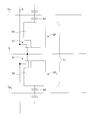
- FIG. 6 is a circuit diagram showing an arrangement configuration of a plurality of pixels arranged on the active area of the liquid crystal display device according to Embodiment 4 of the present invention.
- the sub-pixel electrodes of the two sub-pixels constituting each pixel are arranged to face each other with the same source bus line interposed therebetween.
- each sub-pixel electrode of two sub-pixels constituting each pixel is arranged so as to sandwich two source bus lines.
- the pixel P ⁇ b > 2 includes a subpixel SP ⁇ b > 21 and a subpixel SP ⁇ b > 22 .
- the subpixel SP 21 includes a TFT 21a, an auxiliary capacitor 22a, and a subpixel electrode 23a.
- the subpixel SP 22 includes a TFT 24a, an auxiliary capacitor 25a, and a subpixel electrode 26a.
- TFT21a subpixels SP 21 - gate electrode Gate of TFT21a subpixels SP 21 - gate electrode is connected to the gate bus line G 3, its source electrode is connected to the source bus line S 1.
- the TFT24a subpixels SP 22 gate - gate electrode is connected to the gate bus line G 3, its source electrode is connected to the source bus line S 1.
- the auxiliary capacitor 22a of the sub-pixel SP 21 is formed between the sub-pixel electrode 23a and the auxiliary capacitor bus line Cs XH1 .
- the auxiliary capacitor 25a of the sub-pixel SP 22 is formed between the sub-pixel electrode 26a and the auxiliary capacitor bus line Cs XL2 .
- the sub-pixel SP 21 is disposed in the vicinity of the storage capacitor bus line Cs XH1 .
- the subpixel SP 22 is disposed in the vicinity of the storage capacitor bus line Cs XL2 .
- one rectangular pixel area having a pixel P2 are separated by two sub-pixels SP 21 and SP 22 to predominantly occupy the sides of the long sides (right and left).
- Each sub-pixel SP 21 and SP 22 is connected to two TFTs 21 a and 24 a driven by the same gate bus line G 3 and source bus line S 1 . Note that the sizes of the two TFTs 21a and 24a may be different.
- Two auxiliary capacitor bus line Cs XH1 and the auxiliary capacitor bus line Cs XL2 forms an auxiliary capacitance between the sub-pixels SP 21 and SP 22 of respective one.
- subpixel electrode 23a and the subpixel electrode 26a in FIG. 6 may be replaced with, for example, the subpixel electrode 23b and the subpixel electrode 26b having the shape shown in FIG.
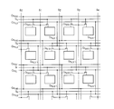
- FIG. 8 is a circuit diagram showing an arrangement configuration of a plurality of pixels arranged on the active area of the liquid crystal display device according to Embodiment 5 of the present invention.
- auxiliary capacitance bus lines Cs XH11 , Cs XH12 , Cs XL11 , Cs XH21 , Cs XL21 , Cs XL22 , Cs XH31 , Cs XH32 , Cs XL31 , Cs XH41 , Cs XL41 , and Cs XL42 are arranged.
- the liquid crystal display devices in the above first to fourth embodiments employ a stripe arrangement used for a display such as a personal computer.
- the liquid crystal display device in the present embodiment adopts a delta arrangement used for video display.
- the delta arrangement is an arrangement in which pixels are shifted every 1/2 pitch for each gate bus line (scanning line).
- the arrangement of pixels, storage capacitor bus lines, and the like is basically the same as the stripe arrangement except that the pitch is shifted.
- the source bus line extends and extends along the edge of the pixel electrode, there is a drawback that the wiring length becomes longer than the stripe arrangement.
- the present embodiment has a structure having two sub-pixels with the source bus line in between, there is an advantage that the data wiring does not have to meander and an efficient layout can be achieved.
- the delta arrangement can obtain a larger aperture ratio than the stripe arrangement, and is very advantageous for video display.
- the auxiliary capacity bus line can be connected as follows.
- a notch is provided in the transparent electrode of the counter substrate so that the above-mentioned connection portions are independent.
- a wiring for establishing conduction between the auxiliary capacitor bus lines is formed on the transparent electrode of the counter substrate after providing an additional insulating film so that conduction between the column spacers for the connection can be obtained. To do.
- the TFT substrate in the present invention is an active matrix TFT substrate in which a plurality of pixels are arranged in a matrix, which includes a first subpixel and a second subpixel adjacent to the first subpixel.
- First and second gate bus lines extending along adjacent directions in which the first and second sub-pixels are adjacent to each other, and the same wiring layer as the first and second gate bus lines
- the first and second auxiliary capacitor bus lines extending along the adjacent direction, the same wiring layer as the first and second gate bus lines, and the first
- a third auxiliary capacitance bus line that is adjacent to one subpixel and forms an auxiliary capacitance of the first subpixel with the subpixel electrode of the first subpixel; and the first and second subpixels Consists of the same wiring layer as the gate bus line
- a fourth auxiliary capacitor bus line that is adjacent to the second subpixel and forms an auxiliary capacitor of the second subpixel between the second subpixel and the subpixel electrode of the second subpixel.
- the first auxiliary capacitor bus line and the first sub-pixel are arranged so as to sandwich the first gate bus line, and the second auxiliary capacitor bus line and the second sub-pixel are The first auxiliary capacity bus line and the second auxiliary capacity bus line are applied with different voltages, and the first auxiliary capacity bus line is sandwiched between the first auxiliary capacity bus line and the second auxiliary capacity bus line.
- the third auxiliary capacitance bus line, the first connection wiring portion composed of a wiring layer different from the first and second gate bus lines, and the second auxiliary capacitance bus Line and the fourth auxiliary capacity Connecting the Surain further includes a second connection wiring part that is composed of a wiring layer different from the first and second gate bus line.
- the first subpixel forms an auxiliary capacitance with the third auxiliary capacitance bus line close to itself.
- the third auxiliary capacitance bus line is connected to the first auxiliary capacitance bus line via a first connection wiring portion configured from a different wiring layer from the first and second gate bus lines.
- the second subpixel forms an auxiliary capacitance with the fourth auxiliary capacitance bus line close to itself.
- the fourth auxiliary capacitance bus line is connected to the second auxiliary capacitance bus line via a second connection wiring portion configured from a different wiring layer from the first and second gate bus lines. Yes.
- the first auxiliary capacitor bus line and the third auxiliary capacitor bus line can be formed in a mesh pattern on the TFT substrate. Further, the second auxiliary capacitor bus line and the fourth auxiliary capacitor bus line can be formed in a mesh pattern on the TFT substrate.
- the same auxiliary capacitance voltage can be uniformly supplied to each pixel on the TFT substrate using the first auxiliary capacitance bus line and the third auxiliary capacitance bus line, and the second auxiliary capacitance bus line can be supplied.
- the same auxiliary capacitance voltage different from the auxiliary capacitance voltage applied to the first auxiliary capacitance bus line can be uniformly supplied to each pixel on the TFT substrate. By doing so, the pixel potential of each pixel in multi-image driving using two different voltages can be held with high accuracy.
- the first connection wiring portion is formed of the same wiring layer as the subpixel electrode of the first subpixel, and the second connection wiring portion is the same as the subpixel electrode of the second subpixel. It is preferable that the wiring layer is configured.
- the wiring structure constituting the TFT substrate can be simplified, the manufacturing cost of the TFT substrate can be reduced.
- the first sub-pixel having a rectangular shape has a first side and a second side located on the opposite side of the first side along the third storage capacitor bus line,
- the storage capacitor bus line includes a first branch line portion close to the first side of the first subpixel and a second branch line portion close to the second side of the first subpixel. It is preferable that
- auxiliary capacitors that is, an auxiliary capacitor using the first branch line portion and an auxiliary capacitor using the second branch line portion can be formed in each sub-pixel.
- the pixel potential of each pixel can be held with higher accuracy.
- the first sub-pixel further includes a third side on the first gate bus line side disposed between the first side and the second side, and the third auxiliary capacitance bus line includes: It is preferable that a third branch line portion adjacent to the third side of the first subpixel is further included.
- auxiliary capacitors that is, an auxiliary capacitor using the first branch line portion, an auxiliary capacitor using the second branch line portion, and an auxiliary capacitor using the third branch line portion are each subpixel. Therefore, the pixel potential of each pixel composed of these sub-pixels can be held with higher accuracy.
- a source bus line that intersects the first and second gate bus lines is further provided, and the first subpixel and the second subpixel are arranged to face each other with the source bus line interposed therebetween. It is preferable.
- the first and second sub-pixels can be arranged so as to face each other with the source bus line interposed therebetween, that is, to be substantially point-symmetric with respect to the source bus line. Further, two pixels composed of the first and second sub-pixels can be arranged to face each other with the third or fourth auxiliary capacitance bus line interposed therebetween. For this reason, a plurality of pixels can be arranged efficiently, and the area occupied by the plurality of pixels can be reduced.
- the first connection wiring portion includes the same wiring layer as the subpixel electrode of the first subpixel and the same wiring layer as the source bus line
- the second connection wiring portion includes the second connection wiring portion.
- the sub-pixel electrode includes the same wiring layer as the sub-pixel electrode and the same wiring layer as the source bus line.
- the wiring structure constituting the TFT substrate can be simplified, the manufacturing cost of the TFT substrate can be reduced.
- the wiring structure constituting the TFT substrate can be simplified, the manufacturing cost of the TFT substrate can be reduced.
- the arrangement of the plurality of pixels is preferably a stripe arrangement.
- the arrangement of the plurality of pixels is preferably a delta arrangement.
- the aperture ratio (light transmittance, effective utilization rate) of each pixel can be improved.
- a liquid crystal display device includes the above-described TFT substrate and a control circuit for controlling an image display process for displaying an image using the TFT substrate.
- the first sub-pixel forms an auxiliary capacitor with the second auxiliary capacitor bus line adjacent to the first sub-pixel.
- the second auxiliary capacitance bus line is connected to the first auxiliary capacitance bus line via a connection wiring portion formed of a wiring layer different from the gate bus line.
- the first auxiliary capacitor bus line and the second auxiliary capacitor bus line can be formed in a mesh pattern on the TFT substrate. Therefore, since the same auxiliary capacitance voltage can be uniformly supplied to each pixel on the TFT substrate using the first auxiliary capacitance bus line and the second auxiliary capacitance bus line, the pixel potential of each pixel is accurately determined. Can hold well.
- the present invention can be applied to various display devices such as a monitor of a personal computer and a television receiver.
- Liquid crystal display device 2 Display unit (TFT substrate) 3 Source Driver 4 Gate Driver 5 Display Control Circuit 6, 7 Cs Control Circuit 11, 14, 21, 21a, 24, 24a, 51, 61 TFT (Thin Film Transistor) 12, 15, 22, 22a, 25, 25a, 27, 28, 29, 30, 52, 62 Auxiliary capacitor 13, 16, 23, 23a, 23b, 26, 26a, 26b, 53, 63 Subpixel electrode 101 Substrate 102 Interlayer insulating film 103 Protective film 104 Wiring layer (first connection wiring portion, second connection wiring portion) Cs YH1 , Cs YH2 , Cs YH3 auxiliary capacity bus line (first auxiliary capacity bus line) Cs YL1 , Cs YL2 , Cs YL3 auxiliary capacity bus line (second auxiliary capacity bus line) Cs XH1 , Cs XH2 auxiliary capacity bus line (third auxiliary capacity bus line) Cs XL1 , Cs XL2 auxiliary capacity bus line (fourth
Abstract
Description
図3は、本発明の実施の形態1における液晶表示装置1の構成を示すブロック図である。本実施の形態における液晶表示装置1は、図3に示すように、アクティブマトリクス型の表示部(TFT基板)2と、ソースドライバ3と、ゲートドライバ(GD)4と、表示制御回路5と、Cs制御回路6及び7と、を備えている。
次に、本発明の実施の形態2について説明する。
次に、本発明の実施の形態3について説明する。
次に、本発明の実施の形態4について説明する。
次に、本発明の実施の形態5について説明する。
(1)対向基板の透明電極に切り欠きを設け、上記の接続部分が独立するようにする。
2 表示部(TFT基板)
3 ソースドライバ
4 ゲートドライバ
5 表示制御回路
6、7 Cs制御回路
11、14、21、21a、24、24a、51、61 TFT(薄膜トランジスタ)
12、15、22、22a、25、25a、27、28、29、30、52、62 補助容量
13、16、23、23a、23b、26、26a、26b、53、63 副画素電極
101 基板
102 層間絶縁膜
103 保護膜
104 配線層(第1の接続配線部、第2の接続配線部)
CsYH1、CsYH2、CsYH3 補助容量バスライン(第1の補助容量バスライン)
CsYL1、CsYL2、CsYL3 補助容量バスライン(第2の補助容量バスライン)
CsXH1、CsXH2 補助容量バスライン(第3の補助容量バスライン)
CsXL1、CsXL2 補助容量バスライン(第4の補助容量バスライン)
S1 ソースバスライン
Claims (10)
- 第1の副画素及び当該第1の副画素に隣接する第2の副画素からなる、複数の画素がマトリクス状に配列されたアクティブマトリクス型のTFT基板であって、
前記第1の副画素及び前記第2の副画素が隣接する隣接方向に沿って延在する第1及び第2のゲートバスラインと、
前記第1及び第2のゲートバスラインと同一の配線層から構成され、且つ、前記隣接方向に沿って延在する第1及び第2の補助容量バスラインと、
前記第1及び第2のゲートバスラインと同一の配線層から構成され、且つ、前記第1の副画素に近接し、前記第1の副画素の副画素電極との間において前記第1の副画素の補助容量を形成する第3の補助容量バスラインと、
前記第1及び第2のゲートバスラインと同一の配線層から構成され、且つ、前記第2の副画素に近接し、前記第2の副画素の副画素電極との間において前記第2の副画素の補助容量を形成する第4の補助容量バスラインと
を備え、
前記第1の補助容量バスラインと前記第1の副画素は、前記第1のゲートバスラインを挟むようにして配置され、前記第2の補助容量バスラインと前記第2の副画素は、前記第2のゲートバスラインを挟むようにして配置されており、
前記第1の補助容量バスラインと前記第2の補助容量バスラインとは、互いに異なる電圧が印加されており、
前記第1の補助容量バスラインと前記第3の補助容量バスラインとの間を接続する、前記第1及び第2のゲートバスラインとは異なる配線層から構成された第1の接続配線部と、
前記第2の補助容量バスラインと前記第4の補助容量バスラインとの間を接続する、前記第1及び第2のゲートバスラインとは異なる配線層から構成された第2の接続配線部と
をさらに備えていることを特徴とするTFT基板。 - 前記第1の接続配線部は、前記第1の副画素の副画素電極と同一の配線層から構成され、前記第2の接続配線部は、前記第2の副画素の副画素電極と同一の配線層から構成されていることを特徴とする請求項1に記載のTFT基板。
- 矩形形状を持つ前記第1の副画素は、前記第3の補助容量バスラインに沿っている、第1辺及び当該第1辺の反対側に位置する第2辺を有し、
前記第3の補助容量バスラインは、前記第1の副画素の第1辺に近接する第1の分岐ライン部分と、前記第1の副画素の第2辺に近接する第2の分岐ライン部分と、を含んでいることを特徴とする請求項1または2に記載のTFT基板。 - 前記第1の副画素は、前記第1辺と前記第2辺と間に配置された前記第1のゲートバスライン側の第3辺をさらに有し、
前記第3の補助容量バスラインは、前記第1の副画素の第3辺に近接する第3の分岐ライン部分をさらに含んでいることを特徴とする請求項3に記載のTFT基板。 - 前記第1及び第2のゲートバスラインと交差するソースバスラインをさらに備え、
前記第1の副画素及び前記第2の副画素は、前記ソースバスラインを挟むようにして対向するように配置されていることを特徴とする請求項1~4のいずれか1項に記載のTFT基板。 - 前記第1の接続配線部は、前記第1の副画素の副画素電極と同一の配線層及び前記ソースバスラインと同一の配線層から構成され、前記第2の接続配線部は、前記第2の副画素の副画素電極と同一の配線層及び前記ソースバスラインと同一の配線層から構成されていることを特徴とする請求項5に記載のTFT基板。
- 前記第1及び第2のゲートバスラインと交差する2つのソースバスラインをさらに備え、
前記第1の副画素及び前記第2の副画素は、隣接する前記2つのソースバスライン間に配置され、且つ、隣接する前記2つのソースバスラインのいずれか一方と接続されていることを特徴とする請求項1~4のいずれか1項に記載のTFT基板。 - 前記複数の画素の配列は、ストライプ配列であることを特徴とする請求項1~7のいずれか1項に記載のTFT基板。
- 前記複数の画素の配列は、デルタ配列であることを特徴とする請求項1~7のいずれか1項に記載のTFT基板。
- 請求項1~9のいずれか1項に記載のTFT基板と、
前記TFT基板を用いて画像を表示するための画像表示処理を制御するための制御回路と
を備えていることを特徴とする液晶表示装置。
Priority Applications (6)
| Application Number | Priority Date | Filing Date | Title |
|---|---|---|---|
| BRPI0924658A BRPI0924658A2 (pt) | 2009-03-24 | 2009-11-05 | substrato tft e aparelho de exibicao de cristal liquido usando o mesmo |
| CN2009801582011A CN102356352A (zh) | 2009-03-24 | 2009-11-05 | Tft基板和使用该tft基板的液晶显示装置 |
| JP2011505679A JP5128703B2 (ja) | 2009-03-24 | 2009-11-05 | Tft基板及びこれを用いた液晶表示装置 |
| US13/257,354 US20120007843A1 (en) | 2009-03-24 | 2009-11-05 | Tft substrate and liquid crystal display apparatus using the same |
| RU2011140079/28A RU2488865C9 (ru) | 2009-03-24 | 2009-11-05 | Подложка, содержащая тонкопленочные транзисторы и жидкокристаллический дисплей, в котором использована такая подложка |
| EP09842174A EP2413181A4 (en) | 2009-03-24 | 2009-11-05 | TFT SUBSTRATE AND LIQUID CRYSTAL DISPLAY APPARATUS USING THE SAME |
Applications Claiming Priority (2)
| Application Number | Priority Date | Filing Date | Title |
|---|---|---|---|
| JP2009072239 | 2009-03-24 | ||
| JP2009-072239 | 2009-03-24 |
Publications (1)
| Publication Number | Publication Date |
|---|---|
| WO2010109558A1 true WO2010109558A1 (ja) | 2010-09-30 |
Family
ID=42780268
Family Applications (1)
| Application Number | Title | Priority Date | Filing Date |
|---|---|---|---|
| PCT/JP2009/005883 WO2010109558A1 (ja) | 2009-03-24 | 2009-11-05 | Tft基板及びこれを用いた液晶表示装置 |
Country Status (7)
| Country | Link |
|---|---|
| US (1) | US20120007843A1 (ja) |
| EP (1) | EP2413181A4 (ja) |
| JP (1) | JP5128703B2 (ja) |
| CN (1) | CN102356352A (ja) |
| BR (1) | BRPI0924658A2 (ja) |
| RU (1) | RU2488865C9 (ja) |
| WO (1) | WO2010109558A1 (ja) |
Cited By (1)
| Publication number | Priority date | Publication date | Assignee | Title |
|---|---|---|---|---|
| JP5538559B2 (ja) * | 2010-11-02 | 2014-07-02 | シャープ株式会社 | 表示装置 |
Families Citing this family (8)
| Publication number | Priority date | Publication date | Assignee | Title |
|---|---|---|---|---|
| US9165948B2 (en) * | 2011-10-31 | 2015-10-20 | Sharp Kabushiki Kaisha | Thin film transistor array substrate and liquid crystal display device |
| CN103474472B (zh) * | 2013-09-10 | 2016-05-11 | 深圳市华星光电技术有限公司 | 一种薄膜晶体管、阵列基板及显示面板 |
| WO2015064477A1 (ja) * | 2013-10-30 | 2015-05-07 | 堺ディスプレイプロダクト株式会社 | 表示パネル |
| CN104362127A (zh) * | 2014-11-21 | 2015-02-18 | 深圳市华星光电技术有限公司 | 薄膜晶体管基板的制作方法及制造设备 |
| CN105404066B (zh) * | 2015-12-28 | 2018-11-23 | 深圳市华星光电技术有限公司 | 阵列基板及液晶显示器 |
| KR102459575B1 (ko) * | 2016-01-06 | 2022-10-27 | 삼성디스플레이 주식회사 | 표시 장치 |
| CN106463545B (zh) * | 2016-07-08 | 2019-11-01 | 京东方科技集团股份有限公司 | 薄膜晶体管及制造方法、阵列基板行驱动电路和显示装置 |
| JP2019191236A (ja) * | 2018-04-19 | 2019-10-31 | シャープ株式会社 | 表示装置 |
Citations (7)
| Publication number | Priority date | Publication date | Assignee | Title |
|---|---|---|---|---|
| JPS62265688A (ja) | 1986-05-13 | 1987-11-18 | 松下電器産業株式会社 | アクテイブマトリツクスアレイ |
| JPH0372321A (ja) | 1989-08-14 | 1991-03-27 | Sharp Corp | アクティブマトリクス表示装置 |
| JPH09160075A (ja) | 1995-12-08 | 1997-06-20 | Casio Comput Co Ltd | 液晶表示素子 |
| JP2001109018A (ja) | 1999-10-12 | 2001-04-20 | Matsushita Electric Ind Co Ltd | 液晶表示装置およびその駆動方法 |
| JP2001281690A (ja) | 2000-03-31 | 2001-10-10 | Fujitsu Ltd | 液晶表示装置及びその修復方法 |
| JP2006098449A (ja) | 2004-09-28 | 2006-04-13 | Seiko Epson Corp | 電気光学装置の製造方法 |
| JP2008158286A (ja) * | 2006-12-25 | 2008-07-10 | Sharp Corp | 液晶表示装置 |
Family Cites Families (13)
| Publication number | Priority date | Publication date | Assignee | Title |
|---|---|---|---|---|
| JP4003714B2 (ja) * | 2003-08-11 | 2007-11-07 | セイコーエプソン株式会社 | 電気光学装置及び電子機器 |
| JP4265788B2 (ja) * | 2003-12-05 | 2009-05-20 | シャープ株式会社 | 液晶表示装置 |
| CN101587274B (zh) * | 2004-10-06 | 2012-01-11 | 夏普株式会社 | 液晶显示器 |
| US7714948B2 (en) * | 2004-12-16 | 2010-05-11 | Sharp Kabushiki Kaisha | Active matrix substrate, method for fabricating active matrix substrate, display device, liquid crystal display device, and television device |
| US7948463B2 (en) * | 2005-03-18 | 2011-05-24 | Sharp Kabushiki Kaisha | Liquid crystal display device |
| KR20060111265A (ko) * | 2005-04-22 | 2006-10-26 | 삼성전자주식회사 | 박막 트랜지스터 기판, 이의 제조 방법 및 이를 갖는 표시장치 |
| JP4799926B2 (ja) * | 2005-06-28 | 2011-10-26 | 三菱電機株式会社 | 半透過型tftアレイ基板、および半透過型液晶表示装置 |
| JP4492483B2 (ja) * | 2005-08-18 | 2010-06-30 | ソニー株式会社 | 液晶表示装置およびその駆動方法 |
| KR101152135B1 (ko) * | 2005-09-12 | 2012-06-15 | 삼성전자주식회사 | 액정 표시 장치 및 그 구동 방법 |
| TWI274221B (en) * | 2005-09-29 | 2007-02-21 | Au Optronics Corp | Active device matrix substrate |
| JP2007199422A (ja) * | 2006-01-26 | 2007-08-09 | Sharp Corp | 液晶表示装置及びその製造方法 |
| CN101153999B (zh) * | 2006-09-29 | 2010-06-23 | 瀚宇彩晶股份有限公司 | 半透射半反射式液晶显示器结构 |
| CN101281329A (zh) * | 2007-04-04 | 2008-10-08 | 瀚宇彩晶股份有限公司 | 液晶显示器及其子像素 |
-
2009
- 2009-11-05 US US13/257,354 patent/US20120007843A1/en not_active Abandoned
- 2009-11-05 BR BRPI0924658A patent/BRPI0924658A2/pt not_active IP Right Cessation
- 2009-11-05 CN CN2009801582011A patent/CN102356352A/zh active Pending
- 2009-11-05 JP JP2011505679A patent/JP5128703B2/ja not_active Expired - Fee Related
- 2009-11-05 WO PCT/JP2009/005883 patent/WO2010109558A1/ja active Application Filing
- 2009-11-05 RU RU2011140079/28A patent/RU2488865C9/ru not_active IP Right Cessation
- 2009-11-05 EP EP09842174A patent/EP2413181A4/en not_active Withdrawn
Patent Citations (7)
| Publication number | Priority date | Publication date | Assignee | Title |
|---|---|---|---|---|
| JPS62265688A (ja) | 1986-05-13 | 1987-11-18 | 松下電器産業株式会社 | アクテイブマトリツクスアレイ |
| JPH0372321A (ja) | 1989-08-14 | 1991-03-27 | Sharp Corp | アクティブマトリクス表示装置 |
| JPH09160075A (ja) | 1995-12-08 | 1997-06-20 | Casio Comput Co Ltd | 液晶表示素子 |
| JP2001109018A (ja) | 1999-10-12 | 2001-04-20 | Matsushita Electric Ind Co Ltd | 液晶表示装置およびその駆動方法 |
| JP2001281690A (ja) | 2000-03-31 | 2001-10-10 | Fujitsu Ltd | 液晶表示装置及びその修復方法 |
| JP2006098449A (ja) | 2004-09-28 | 2006-04-13 | Seiko Epson Corp | 電気光学装置の製造方法 |
| JP2008158286A (ja) * | 2006-12-25 | 2008-07-10 | Sharp Corp | 液晶表示装置 |
Non-Patent Citations (1)
| Title |
|---|
| See also references of EP2413181A4 * |
Cited By (1)
| Publication number | Priority date | Publication date | Assignee | Title |
|---|---|---|---|---|
| JP5538559B2 (ja) * | 2010-11-02 | 2014-07-02 | シャープ株式会社 | 表示装置 |
Also Published As
| Publication number | Publication date |
|---|---|
| EP2413181A1 (en) | 2012-02-01 |
| JPWO2010109558A1 (ja) | 2012-09-20 |
| US20120007843A1 (en) | 2012-01-12 |
| RU2488865C9 (ru) | 2014-01-20 |
| RU2488865C2 (ru) | 2013-07-27 |
| RU2011140079A (ru) | 2013-04-27 |
| CN102356352A (zh) | 2012-02-15 |
| EP2413181A4 (en) | 2012-08-29 |
| JP5128703B2 (ja) | 2013-01-23 |
| BRPI0924658A2 (pt) | 2016-01-26 |
Similar Documents
| Publication | Publication Date | Title |
|---|---|---|
| JP5128703B2 (ja) | Tft基板及びこれを用いた液晶表示装置 | |
| JP5314155B2 (ja) | 液晶表示装置 | |
| US8228287B2 (en) | Liquid crystal display device for removing ripple voltage and method of driving the same | |
| KR101623593B1 (ko) | 액정표시장치 | |
| US20140078430A1 (en) | Horizontal Stripe Liquid Crystal Display Device | |
| US20130141660A1 (en) | Array substrate and display device | |
| KR20100055154A (ko) | 액정 표시 장치 및 그의 구동 방법 | |
| JP2014232332A (ja) | 液晶パネル | |
| US20180231814A1 (en) | Pixel structure, driving method thereof, display substrate and display device | |
| JP4428255B2 (ja) | 電気光学装置、駆動方法および電子機器 | |
| JP5095821B2 (ja) | 表示装置 | |
| US9336737B2 (en) | Array substrate, display device and control method thereof | |
| JP4163611B2 (ja) | 液晶表示装置 | |
| EP2998785B1 (en) | Liquid crystal display panel and driving method therefor | |
| US8384703B2 (en) | Liquid crystal display device | |
| JP5789354B2 (ja) | 電気光学装置及び電子機器 | |
| KR101171184B1 (ko) | 표시 장치 | |
| JP2017142312A (ja) | 液晶表示パネル、液晶表示装置、および液晶表示パネルの製造方法 | |
| KR20120090888A (ko) | 액정 표시 장치 | |
| JP2011164236A (ja) | 表示装置 | |
| JPWO2016143097A1 (ja) | 液晶表示パネル | |
| JP4612100B2 (ja) | 液晶表示装置及びこれの製造方法 | |
| WO2022193440A1 (zh) | 显示面板及显示装置 | |
| WO2018061094A1 (ja) | 表示装置 | |
| KR20120029266A (ko) | 액정표시장치 |
Legal Events
| Date | Code | Title | Description |
|---|---|---|---|
| WWE | Wipo information: entry into national phase |
Ref document number: 200980158201.1 Country of ref document: CN |
|
| 121 | Ep: the epo has been informed by wipo that ep was designated in this application |
Ref document number: 09842174 Country of ref document: EP Kind code of ref document: A1 |
|
| ENP | Entry into the national phase |
Ref document number: 2011505679 Country of ref document: JP Kind code of ref document: A |
|
| WWE | Wipo information: entry into national phase |
Ref document number: 13257354 Country of ref document: US |
|
| NENP | Non-entry into the national phase |
Ref country code: DE |
|
| WWE | Wipo information: entry into national phase |
Ref document number: 6972/CHENP/2011 Country of ref document: IN Ref document number: 2009842174 Country of ref document: EP |
|
| ENP | Entry into the national phase |
Ref document number: 2011140079 Country of ref document: RU Kind code of ref document: A |
|
| REG | Reference to national code |
Ref country code: BR Ref legal event code: B01A Ref document number: PI0924658 Country of ref document: BR |
|
| ENP | Entry into the national phase |
Ref document number: PI0924658 Country of ref document: BR Kind code of ref document: A2 Effective date: 20110921 |