WO2010095490A1 - 半導体装置の製造方法およびボンディング装置 - Google Patents
半導体装置の製造方法およびボンディング装置 Download PDFInfo
- Publication number
- WO2010095490A1 WO2010095490A1 PCT/JP2010/050910 JP2010050910W WO2010095490A1 WO 2010095490 A1 WO2010095490 A1 WO 2010095490A1 JP 2010050910 W JP2010050910 W JP 2010050910W WO 2010095490 A1 WO2010095490 A1 WO 2010095490A1
- Authority
- WO
- WIPO (PCT)
- Prior art keywords
- capillary
- bonding
- initial ball
- pressure contact
- pad surface
- Prior art date
- Legal status (The legal status is an assumption and is not a legal conclusion. Google has not performed a legal analysis and makes no representation as to the accuracy of the status listed.)
- Ceased
Links
Images






Classifications
-
- B—PERFORMING OPERATIONS; TRANSPORTING
- B23—MACHINE TOOLS; METAL-WORKING NOT OTHERWISE PROVIDED FOR
- B23K—SOLDERING OR UNSOLDERING; WELDING; CLADDING OR PLATING BY SOLDERING OR WELDING; CUTTING BY APPLYING HEAT LOCALLY, e.g. FLAME CUTTING; WORKING BY LASER BEAM
- B23K20/00—Non-electric welding by applying impact or other pressure, with or without the application of heat, e.g. cladding or plating
- B23K20/10—Non-electric welding by applying impact or other pressure, with or without the application of heat, e.g. cladding or plating making use of vibrations, e.g. ultrasonic welding
-
- B—PERFORMING OPERATIONS; TRANSPORTING
- B23—MACHINE TOOLS; METAL-WORKING NOT OTHERWISE PROVIDED FOR
- B23K—SOLDERING OR UNSOLDERING; WELDING; CLADDING OR PLATING BY SOLDERING OR WELDING; CUTTING BY APPLYING HEAT LOCALLY, e.g. FLAME CUTTING; WORKING BY LASER BEAM
- B23K20/00—Non-electric welding by applying impact or other pressure, with or without the application of heat, e.g. cladding or plating
- B23K20/002—Non-electric welding by applying impact or other pressure, with or without the application of heat, e.g. cladding or plating specially adapted for particular articles or work
- B23K20/004—Wire welding
- B23K20/005—Capillary welding
- B23K20/007—Ball bonding
-
- H—ELECTRICITY
- H10—SEMICONDUCTOR DEVICES; ELECTRIC SOLID-STATE DEVICES NOT OTHERWISE PROVIDED FOR
- H10W—GENERIC PACKAGES, INTERCONNECTIONS, CONNECTORS OR OTHER CONSTRUCTIONAL DETAILS OF DEVICES COVERED BY CLASS H10
- H10W72/00—Interconnections or connectors in packages
- H10W72/01—Manufacture or treatment
- H10W72/015—Manufacture or treatment of bond wires
- H10W72/01551—Changing the shapes of bond wires
-
- H—ELECTRICITY
- H10—SEMICONDUCTOR DEVICES; ELECTRIC SOLID-STATE DEVICES NOT OTHERWISE PROVIDED FOR
- H10W—GENERIC PACKAGES, INTERCONNECTIONS, CONNECTORS OR OTHER CONSTRUCTIONAL DETAILS OF DEVICES COVERED BY CLASS H10
- H10W72/00—Interconnections or connectors in packages
- H10W72/071—Connecting or disconnecting
- H10W72/0711—Apparatus therefor
- H10W72/07141—Means for applying energy, e.g. ovens or lasers
-
- H—ELECTRICITY
- H10—SEMICONDUCTOR DEVICES; ELECTRIC SOLID-STATE DEVICES NOT OTHERWISE PROVIDED FOR
- H10W—GENERIC PACKAGES, INTERCONNECTIONS, CONNECTORS OR OTHER CONSTRUCTIONAL DETAILS OF DEVICES COVERED BY CLASS H10
- H10W72/00—Interconnections or connectors in packages
- H10W72/071—Connecting or disconnecting
- H10W72/0711—Apparatus therefor
- H10W72/07173—Means for moving chips, wafers or other parts, e.g. conveyor belts
-
- H—ELECTRICITY
- H10—SEMICONDUCTOR DEVICES; ELECTRIC SOLID-STATE DEVICES NOT OTHERWISE PROVIDED FOR
- H10W—GENERIC PACKAGES, INTERCONNECTIONS, CONNECTORS OR OTHER CONSTRUCTIONAL DETAILS OF DEVICES COVERED BY CLASS H10
- H10W72/00—Interconnections or connectors in packages
- H10W72/071—Connecting or disconnecting
- H10W72/0711—Apparatus therefor
- H10W72/07183—Means for monitoring
-
- H—ELECTRICITY
- H10—SEMICONDUCTOR DEVICES; ELECTRIC SOLID-STATE DEVICES NOT OTHERWISE PROVIDED FOR
- H10W—GENERIC PACKAGES, INTERCONNECTIONS, CONNECTORS OR OTHER CONSTRUCTIONAL DETAILS OF DEVICES COVERED BY CLASS H10
- H10W72/00—Interconnections or connectors in packages
- H10W72/071—Connecting or disconnecting
- H10W72/075—Connecting or disconnecting of bond wires
- H10W72/07511—Treating the bonding area before connecting, e.g. by applying flux or cleaning
-
- H—ELECTRICITY
- H10—SEMICONDUCTOR DEVICES; ELECTRIC SOLID-STATE DEVICES NOT OTHERWISE PROVIDED FOR
- H10W—GENERIC PACKAGES, INTERCONNECTIONS, CONNECTORS OR OTHER CONSTRUCTIONAL DETAILS OF DEVICES COVERED BY CLASS H10
- H10W72/00—Interconnections or connectors in packages
- H10W72/071—Connecting or disconnecting
- H10W72/075—Connecting or disconnecting of bond wires
- H10W72/07521—Aligning
-
- H—ELECTRICITY
- H10—SEMICONDUCTOR DEVICES; ELECTRIC SOLID-STATE DEVICES NOT OTHERWISE PROVIDED FOR
- H10W—GENERIC PACKAGES, INTERCONNECTIONS, CONNECTORS OR OTHER CONSTRUCTIONAL DETAILS OF DEVICES COVERED BY CLASS H10
- H10W72/00—Interconnections or connectors in packages
- H10W72/071—Connecting or disconnecting
- H10W72/075—Connecting or disconnecting of bond wires
- H10W72/07531—Techniques
- H10W72/07532—Compression bonding, e.g. thermocompression bonding
- H10W72/07533—Ultrasonic bonding, e.g. thermosonic bonding
-
- H—ELECTRICITY
- H10—SEMICONDUCTOR DEVICES; ELECTRIC SOLID-STATE DEVICES NOT OTHERWISE PROVIDED FOR
- H10W—GENERIC PACKAGES, INTERCONNECTIONS, CONNECTORS OR OTHER CONSTRUCTIONAL DETAILS OF DEVICES COVERED BY CLASS H10
- H10W72/00—Interconnections or connectors in packages
- H10W72/50—Bond wires
- H10W72/531—Shapes of wire connectors
- H10W72/536—Shapes of wire connectors the connected ends being ball-shaped
-
- H—ELECTRICITY
- H10—SEMICONDUCTOR DEVICES; ELECTRIC SOLID-STATE DEVICES NOT OTHERWISE PROVIDED FOR
- H10W—GENERIC PACKAGES, INTERCONNECTIONS, CONNECTORS OR OTHER CONSTRUCTIONAL DETAILS OF DEVICES COVERED BY CLASS H10
- H10W72/00—Interconnections or connectors in packages
- H10W72/50—Bond wires
- H10W72/541—Dispositions of bond wires
- H10W72/5449—Dispositions of bond wires not being orthogonal to a side surface of the chip, e.g. fan-out arrangements
-
- H—ELECTRICITY
- H10—SEMICONDUCTOR DEVICES; ELECTRIC SOLID-STATE DEVICES NOT OTHERWISE PROVIDED FOR
- H10W—GENERIC PACKAGES, INTERCONNECTIONS, CONNECTORS OR OTHER CONSTRUCTIONAL DETAILS OF DEVICES COVERED BY CLASS H10
- H10W90/00—Package configurations
- H10W90/701—Package configurations characterised by the relative positions of pads or connectors relative to package parts
- H10W90/751—Package configurations characterised by the relative positions of pads or connectors relative to package parts of bond wires
- H10W90/754—Package configurations characterised by the relative positions of pads or connectors relative to package parts of bond wires between a chip and a stacked insulating package substrate, interposer or RDL
-
- H—ELECTRICITY
- H10—SEMICONDUCTOR DEVICES; ELECTRIC SOLID-STATE DEVICES NOT OTHERWISE PROVIDED FOR
- H10W—GENERIC PACKAGES, INTERCONNECTIONS, CONNECTORS OR OTHER CONSTRUCTIONAL DETAILS OF DEVICES COVERED BY CLASS H10
- H10W90/00—Package configurations
- H10W90/701—Package configurations characterised by the relative positions of pads or connectors relative to package parts
- H10W90/751—Package configurations characterised by the relative positions of pads or connectors relative to package parts of bond wires
- H10W90/756—Package configurations characterised by the relative positions of pads or connectors relative to package parts of bond wires between a chip and a stacked lead frame, conducting package substrate or heat sink
Definitions
- the present invention relates to a semiconductor device manufacturing method and a bonding apparatus for bonding a bonding target.
- an initial ball is formed at the tip of a bonding wire drawn out from a capillary, and the initial ball is applied by applying ultrasonic vibration in a state where the initial ball is in pressure contact with a pad surface of a semiconductor device.
- First bonding is performed to be fixed to the pad surface.
- the bonding wire is drawn out from the capillary to form a wire loop, and the bonding wire and the capillary are brought into pressure contact with the lead surface of the substrate, thereby fixing the bonding wire to the lead surface and cutting the bonding wire. Bonding is in progress.
- the initial ball may not be securely fixed to the pad surface during the first bonding, and during the second bonding. There is a problem that the bonding wire may not be cut.
- the present invention provides a method of manufacturing a semiconductor device and a bonding apparatus capable of improving the bonding accuracy by reducing the collapse amount of the initial ball when bonding the initial ball to the pad surface of the semiconductor device.
- Another object of the present invention is to provide a semiconductor device manufacturing method and a bonding apparatus capable of improving the cutting performance of the bonding wire fixed to the lead surface when bonding the bonding wire to the lead surface of the substrate.
- a method for manufacturing a semiconductor device includes a bonding stage on which a bonding target provided with a pad surface is placed, a capillary through which a bonding wire having an initial ball formed at the tip is inserted, and a bonding stage.
- a pressure contact means for pressurizing and contacting the initial ball to the pad surface to be bonded; and when the initial ball is in pressure contact with the pad surface, the capillary is swirled in a direction orthogonal to the pressure direction of the initial ball.
- a bonding target pad placed on the bonding stage by a step of preparing a bonding apparatus including a control unit having a scrubbing means that rotates in a shape, and a pressure contact unit based on a command from the control unit of the bonding apparatus On the surface, the tip of the bonding wire inserted through the capillary
- a scrubbing step of rotating the capillary in a spiral shape in a direction perpendicular to
- the pad surface and the initial ball are in pressure contact with each other by rotating the capillary. Since they are rubbed together, the initial ball is fixed to the pad surface. At this time, by rotating the capillary in a spiral shape, the force applied to the initial ball can be converged in the direction of the center of rotation, so that sufficient time and distance for rubbing the pad surface and the initial ball are secured. The time and distance at which the pad surface and the initial ball are rubbed together with the maximum diameter can be reduced. As a result, the collapse amount of the initial ball can be reduced, so that the bonding accuracy can be improved and the pad pitch, which is the distance between the pad surfaces, can be reduced.
- the scrubbing step uses the position where the initial ball contacts the pad surface as a reference position, rotates the capillary spirally while increasing the diameter from the reference position, and then spirals the capillary while reducing the diameter. It is preferable to rotate it back to the reference position.
- the capillary is rotated in a spiral shape while increasing the diameter, with the position where the initial ball contacts the pad surface as a reference position, and then the capillary is rotated in a spiral shape while reducing the diameter.
- the capillary In the scrubbing step, when the pad surface is extended, it is preferable to rotate the capillary into a flat spiral shape along the extending direction of the pad surface. According to this method for manufacturing a semiconductor device, since the capillary is rotated in a spiral shape along the extending direction of the pad surface, the shape of the initial ball fixed to the pad surface can be adapted to the shape of the pad surface. it can. For this reason, it is possible to improve the bonding accuracy even for the pad surface extending in an arbitrary direction.
- a bonding apparatus includes a bonding stage on which a bonding target provided with a pad surface is placed, a capillary through which a bonding wire having an initial ball formed at the tip is inserted, and a bonding placed on the bonding stage.
- Pressurizing contact means that presses the initial ball against the target pad surface, and when the initial ball is in pressure contact with the pad surface, the capillary rotates spirally in a direction perpendicular to the initial ball pressing direction.
- a controller having scrubbing means.
- the bonding apparatus of the present invention when the initial ball is brought into pressure contact with the pad surface to be bonded, the pad surface and the initial ball are rubbed in the pressure contact state by rotating the capillary. Therefore, the initial ball is fixed to the pad surface. At this time, by rotating the capillary in a spiral shape, the force applied to the initial ball can be converged in the direction of the center of rotation, so that sufficient time and distance for rubbing the pad surface and the initial ball are secured. The time and distance at which the pad surface and the initial ball are rubbed together with the maximum diameter can be reduced. As a result, the collapse amount of the initial ball generated by moving the capillary can be reduced, so that the bonding accuracy can be improved and the pad pitch, which is the distance between the pad surfaces, can be reduced. .
- the method for manufacturing a semiconductor device includes a bonding stage on which a bonding target provided with a lead surface is placed, a capillary through which a bonding wire is inserted, and a bonding target lead surface placed on the bonding stage.
- the pressure direction of the capillary when the capillary is in pressure contact with the lead surface by the pressure contact step of pressing the bonding wire inserted through the capillary and the scrubbing means based on the command of the controller of the bonding apparatus And a scrubbing step of rotating the capillary in a spiral shape in a direction perpendicular to.
- the bonding wire is fixed to the lead surface, and the bonding is performed.
- the wire is sandwiched between the capillary and the lead surface and cut. Then, by rotating the capillary in a spiral shape, the capillary is rubbed in a spiral shape while being in pressure contact with the lead surface, thereby reducing the bonding wire cutting error and improving the bonding wire cutting performance. be able to.
- the scrubbing step uses the position where the capillary contacts the lead surface as a reference position, rotates the capillary spirally while increasing the diameter from the reference position, and then spirals the capillary while reducing the diameter. It is preferable to rotate it back to the reference position.
- the capillary is rotated in a spiral shape while increasing the diameter, with the position where the capillary and the bonding wire are in contact with the lead surface as the reference position, and then the capillary is spiraled while reducing the diameter.
- the displacement between the position where the capillary is in pressure contact with the lead surface and the position of the indentation of the capillary generated on the lead surface when the capillary is in pressure contact can be reduced. .
- the lead pitch which is the distance between the lead surfaces.
- the shape of the indentation of the capillary formed on the lead surface is adapted to the shape of the lead surface in order to rotate the capillary in a spiral shape that is flat along the extending direction of the lead surface. Can do. For this reason, it is possible to improve the bonding accuracy even for a lead surface extending in an arbitrary direction.
- a bonding apparatus includes a bonding stage on which a bonding target provided with a lead surface is mounted, a capillary through which a bonding wire is inserted, a lead on the bonding target mounted on the bonding stage, and a capillary and Pressurizing contact means for pressurizing and contacting the bonding wire inserted through the capillary, and when the capillary is in press contact with the lead surface, the capillary is rotated in a spiral shape in a direction perpendicular to the pressurizing direction of the capillary And a controller having scrubbing means.
- the bonding wire when the capillary and the bonding wire inserted through the capillary are brought into pressure contact with the lead surface to be bonded, the bonding wire is fixed to the lead surface, and the bonding wire is connected to the capillary. And is cut between the lead surfaces. Then, by rotating the capillary on which the bonding target is placed in a spiral shape, the capillary is rubbed in a spiral shape while being in pressure contact with the lead surface, thereby reducing bonding wire cutting errors and bonding. The cutting property of the wire can be improved.
- the collapse accuracy of the initial ball can be reduced and the bonding accuracy can be improved.
- the cutting performance of the bonding wire fixed to the lead surface can be improved.
- FIG. 2 It is the figure which showed an example of the wire bonding apparatus which concerns on 1st Embodiment. It is a flowchart which shows the bonding method using a wire bonding apparatus.
- 3 is a flowchart showing a first bonding step shown in FIG. 2.
- 3 is a flowchart showing a second bonding step shown in FIG. 2.
- (A) is the figure which showed the movement locus
- (b) is the figure which showed the command position for driving an X-axis linear motor and a Y-axis linear motor. It is a figure which shows the temporary command position of X-axis, and the temporary command position of Y-axis.
- (A) has shown the enlarged photograph of the lead surface in a comparative example
- (b) has shown the enlarged photograph of the lead surface in an Example. It is a graph which shows the tensile strength of the bonding wire fixed to the lead surface.
- (A) is the figure which showed the movement locus
- (b) drives the X-axis linear motor and Y-axis linear motor in the case of (a). It is the figure which showed the command position for making it.
- (A) is the figure which showed the movement locus
- (b) drives the X-axis linear motor and Y-axis linear motor in the case of (a). It is the figure which showed the command position for making it.
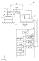
- FIG. 1 is a diagram illustrating an example of a wire bonding apparatus according to the first embodiment.
- the wire bonding apparatus 10 according to the first embodiment includes a pad surface 2 provided in the semiconductor device 1 by wire bonding using a bonding wire 11 inserted through a capillary 12, The lead surface 4 provided on the substrate 3 to which the semiconductor device 1 is bonded is electrically connected.
- the wire bonding apparatus 10 includes a capillary 12 through which the bonding wire 11 is inserted, a bonding head 15 that holds the capillary 12, an arm drive motor 16 that rotates (swings) the bonding head 15, and a substrate to be bonded.
- a bonding stage 17 on which 3 is mounted an XY moving mechanism 18 that moves the bonding head 15 in the X-axis direction and the Y-axis direction, which are horizontal directions, a control unit 20 that comprehensively controls the wire bonding apparatus 10, It has.
- the bonding head 15 extends from the bonding head 15 toward the bonding stage 17, and includes an ultrasonic horn 13 provided with a vibrator 13a that holds the capillary 12 at one end and generates ultrasonic vibration at the other end. It comprises a bonding arm 14 that holds a sonic horn 13. Therefore, by rotating the arm drive motor 16, the ultrasonic horn 13 moves the capillary 12 in the Z-axis direction, which is the vertical direction, so that the substrate 3 and the semiconductor device 1 placed on the bonding stage 17 are moved. The bonding wire 11 can be bonded. Then, by generating ultrasonic vibration from the vibrator 13 a of the ultrasonic horn 13, the capillary 12 held by the bonding arm 14 can be vibrated.
- the arm drive motor 16 moves the capillary 12 in the Z-axis direction, which is the vertical direction, by rotating (swinging).
- the arm drive motor 16 can adjust the load applied to the capillary 12 by adjusting the output torque of the rotational drive.
- the XY moving mechanism 18 moves the bonding head 15 in the X-axis direction and moves the bonding head 15 in the Y-axis direction. Therefore, the XY moving mechanism 18 is provided with an X-axis linear motor 18a that moves the bonding head 15 in the X-axis direction and a Y-axis linear motor 18b that moves the bonding head 15 in the Y-axis direction.
- the XY moving mechanism 18 is constituted by, for example, a linear motor mechanism, and the bonding head 15 moves in the X-axis direction and the Y-axis direction as the X-axis linear motor 18a and the Y-axis linear motor 18b rotate. It becomes possible to do.
- the bonding head 15 moves in the X-axis direction and the Y-axis direction, thereby moving the capillary 12 in the X-axis direction and the Y-axis direction.
- the control unit 20 is electrically connected to the ultrasonic horn 13 (vibrator 13a), the arm drive motor 16, the X-axis linear motor 18a, and the Y-axis linear motor 18b, and the ultrasonic horn 13, the arm drive motor 16, Wire bonding is performed by controlling the X-axis linear motor 18a and the Y-axis linear motor 18b.
- control unit 20 is bonded to the substrate 3 placed on the bonding stage 17 in the first bonding step of bonding the bonding wire 11 inserted through the capillary 12 to the pad surface 2 provided in the semiconductor device 1.
- a scrub function (means) for rotating the capillary 12 in a spiral shape in a direction orthogonal to the pressurizing direction of 11a.
- control unit 20 applies the bonding wire 11 bonded to the pad surface 2 to the lead surface 4 of the substrate 3 placed on the bonding stage 17 in the second bonding step of bonding the bonding wire 11 to the lead surface 4 provided on the substrate 3.
- the pressure contact function (means) that pressurizes and contacts the capillary 12 and the initial ball 11 a of the bonding wire 11 inserted through the capillary 12, and when the capillary 12 is in pressure contact with the lead surface 4,
- the pressure contact function and the scrub function are realized by executing a pressure contact program and a scrub program stored in a storage device or the like.
- the control unit 20 includes an arm drive motor I / F 21 that transmits and receives signals to and from the arm drive motor 16, and an ultrasonic horn I / F 22 that transmits and receives signals to and from the ultrasonic horn 13.
- the X-axis linear motor I / F 23 that transmits and receives signals to and from the X-axis linear motor 18a
- the Y-axis linear motor I / F 24 that transmits and receives signals to and from the Y-axis linear motor 18b
- a keyboard An input unit 25 that receives input of various control information from an operator, an output unit 26 that is a display device such as a monitor and displays various control information of the control unit 20, and various programs are stored.
- a memory 27 and a CPU 28 for performing bonding control are provided.
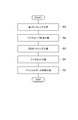
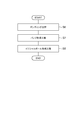
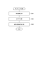
- FIG. 2 is a flowchart showing a bonding method using a wire bonding apparatus.
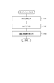
- FIG. 3 is a flowchart showing the first bonding step shown in FIG.
- FIG. 4 is a flowchart showing the second bonding step shown in FIG.
- the processing operation of the wire bonding apparatus 10 described below is performed by performing a pressure contact function as a pressure contact program based on a command from the control unit 20 or a scrub function as a scrub program.
- the wire bonding apparatus 10 first performs a first bonding process (step S1).
- step S11 a pressure contact process is performed (step S11).
- the capillary 12 is lowered by rotating the arm drive motor 16.
- the initial ball 11 a comes into contact with the pad surface 2 by lowering the capillary 12.
- a predetermined load is applied to the initial ball 11a through the capillary 12, and the initial ball 11a is applied to the pad surface. 2 is brought into pressure contact.
- a scrub process is performed (step S12).
- a scrubbing step when the initial ball 11a is brought into pressure contact with the pad surface 2, a scrubbing operation is performed in which the bonding head 15 is moved to rotate the capillary 12 in a spiral shape. Note that the scrubbing operation may be performed during any period regardless of the generation period of ultrasonic vibration in the ultrasonic vibration application process described later, as long as the scrub operation is performed while the initial ball 11a is in pressure contact with the pad surface 2. .
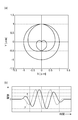
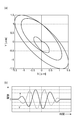
- FIG. 5A is a diagram showing the movement trajectory of the capillary that performs the scrubbing operation
- FIG. 5B is a diagram showing the command position for driving the X-axis linear motor and the Y-axis linear motor. is there.
- the scrubbing operation is performed by driving the X-axis linear motor and the Y-axis linear motor to rotate the capillary 12 held by the bonding head 15 in a spiral shape, thereby causing the initial ball 11a to move.
- the pad surface 2 is rotated in a spiral shape.
- the position when the initial ball 11a contacts the pad surface 2 is defined as the reference position (0, 0). Then, the capillary 12 is rotated in a spiral shape while increasing the rotation radius from the reference position. When the rotation radius is maximized, the capillary 12 is rotated in a spiral shape while reducing the rotation radius. Return to the reference position.
- the pad surface 2 is a 35 ⁇ m square and the initial ball 11a is a sphere having a diameter of 20 ⁇ m
- the maximum diameter (diameter) to be rotated in a spiral shape is about 20 ⁇ m.
- control unit 20 controls the driving of the X-axis linear motor 18a and the Y-axis linear motor 18b based on the X-axis command position x and the Y-axis command position y shown in FIG. Is done.
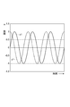
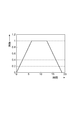
- FIG. 6 is a diagram illustrating an X-axis temporary command position and a Y-axis temporary command position.
- FIG. 7 is a diagram showing an operation ratio of the X-axis temporary command position and the Y-axis temporary command position.
- an X-axis temporary command position x1 that is the X-axis command position and a Y-axis temporary command position y1 that is the Y-axis command position
- the X-axis temporary command position x1 is fitted with a three-cycle sine curve
- the Y-axis temporary command position y1 is fitted with a three-cycle cosine curve that is 90 ° out of phase with the X-axis temporary command position x1.
- the operation ratios of the X-axis temporary command position x1 and the Y-axis temporary command position y1 are created. That is, the operation ratio shown in FIG. 7 indicates the speed ratio at which the capillary 12 moves. This operation rate rises linearly from 0 to 1 in the first cycle, maintains 1 in the next cycle, and falls linearly from 1 to 0 in the last cycle. As a result, the moving speed of the capillary 12 is linearly accelerated from the speed ratio 0 to the speed ratio 1 in the first period, and becomes a constant speed at the speed ratio 1 in the second period. The speed is linearly decelerated from the ratio 1 state to reach the speed ratio 0, and the vehicle is stopped.
- the X-axis command position x and the Y-axis command position shown in FIG. 5B are combined with the X-axis provisional command position x1 and the Y-axis provisional command position y1 shown in FIG. y is calculated.
- the initial ball 11a and the pad surface 2 are rubbed together, so that an oxide film (not shown) formed on the surface layer of the pad surface 2 is formed.
- the initial ball 11a is fixed to the pad surface 2 by breaking.
- the initial ball 11a is crushed by rubbing against the pad surface 2 to generate a crushed allowance 11b that is pushed outward in the radial direction of the scrubbing operation.
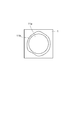
- the capillary 12 by rotating the capillary 12 in a spiral shape as a scrubbing operation, the time and distance at which the initial ball 11a and the pad surface 2 are rubbed with each other when the capillary 12 is rotated at the maximum diameter are shortened, and the initial ball is shortened. Since the force applied to 11a can be converged in the direction of the rotation center, the crushing margin 11b does not spread and its generation is suppressed.
- an ultrasonic vibration application step is performed (step S13).
- the ultrasonic vibration application step when the initial ball 11 a is pressed against the pad surface 2, ultrasonic vibration is generated from the vibrator 13 a of the ultrasonic horn 13. Then, the ultrasonic vibration generated by the vibrator 13 a is transmitted to the initial ball 11 a via the ultrasonic horn 13 and the capillary 12. Then, the initial ball 11a is vibrated ultrasonically, whereby the initial ball 11a and the pad surface 2 are finely rubbed, and the initial ball 11a is firmly fixed to the lead surface 4.
- a wire loop forming process is performed as shown in FIG. 2 (step S2).
- a wire loop is formed while the bonding wire 11 having the initial ball 11 a fixed to the pad surface 2 is fed out from the capillary 12, and the bonding wire 11 is brought into contact with the lead surface 4.
- step S3 a second bonding process is performed.
- a pressure contact process is first performed (step S31).
- the capillary 12 is lowered by rotating the arm drive motor 16 to bring the bonding wire 11 and the capillary 12 into contact with the lead surface 4. That is, by adjusting the output torque of the arm drive motor 16, a predetermined load is applied to the capillary 12, and the capillary 12 is brought into pressure contact with the lead surface 4 to such an extent that the bonding wire 11 is crushed by the capillary 12. . Thereby, the bonding wire 11 is fixed to the lead surface 4.
- a scrub process is performed (step S32).
- a scrubbing operation for rotating the capillary 12 in a spiral shape is performed as in the scrubbing process (step S12) in the first bonding process (step S1). Then, by this scrubbing operation, the bonding wire 11 is crushed between the capillary 12 and the lead surface 4.
- an ultrasonic vibration application step is performed (step S33).
- ultrasonic vibration is generated from the vibrator 13a of the ultrasonic horn 13 and applied to the initial ball 11a. Apply ultrasonic vibration. Then, the initial ball 11 a is fixed to the lead surface 4.
- a wire cutting process is performed as shown in FIG. 2 (step S4).
- the wire cutting process first, the capillary 12 is raised by rotating the arm drive motor 16 and the bonding wire 11 is fed out of the capillary 12 by a predetermined length. Then, the tail of the bonding wire 11 is cut by raising the capillary 12 again with the bonding wire 11 clamped (not shown). Thereby, the pad surface 2 and the lead surface 4 are electrically connected by the bonding wire 11 in which the wire loop is formed.
- an initial ball forming process is performed (step 5).
- the tail (tip portion) of the bonding wire 11 cut in the wire cutting step (step S4) is discharged by an electric torch to form a spherical initial ball 11a on the tail of the bonding wire 11.
- FIG. 9 is a diagram illustrating an example of a bump bonding apparatus according to the second embodiment.
- the bump bonding apparatus 30 according to the second embodiment is configured such that each of one or a plurality of semiconductor devices 7 fixed to the substrate 6 is bonded by bonding a bonding wire 11 inserted through the capillary 12. Bumps are formed on the pad surface 8 formed in the above.
- the bump bonding apparatus 30 has the same basic configuration as the wire bonding apparatus 10 according to the first embodiment, although the bonding target and the bonding method are different.
- the bump bonding apparatus 30 is similar to the wire bonding apparatus 10 in that the capillary 12 into which the bonding wire 11 is inserted, the bonding head 15 that holds the capillary, and the arm drive motor that rotates (swings) the bonding head 15. 16, a bonding stage 17 on which a substrate 6 to be bonded is placed, an XY moving mechanism 18 that moves the bonding stage 17 in the horizontal X-axis direction and the Y-axis direction, and a bump bonding apparatus 30. And a control unit 40 for controlling.
- the bonding head 15 includes an ultrasonic horn 13 provided with a vibrator 13 a that holds the capillary 12 at one end and generates ultrasonic vibration at the other end, and a bonding arm 14 that holds the ultrasonic horn 13. Has been.
- the control unit 40 is electrically connected to the ultrasonic horn 13 (vibrator 13a), the arm drive motor 16, the X-axis linear motor 18a, and the Y-axis linear motor 18b, and the ultrasonic horn 13, the arm drive motor 16, Bumps are formed on the pad surface 8 of the semiconductor device 7 by controlling the X-axis linear motor 18a and the Y-axis linear motor 18b.
- control unit 40 is a semiconductor bonded to the substrate 6 placed on the bonding stage 17 in the bonding step of bonding the bonding wire 11 inserted into the capillary 12 to the pad surface 8 provided in the semiconductor device 7.
- a scrubbing function (means) for rotating the capillary 12 in a spiral shape in a direction orthogonal to the pressurizing direction.
- the control unit 40 transmits / receives a signal to / from the arm drive motor 16. Therefore, the control unit 40 transmits / receives a signal to / from the arm drive motor 16.
- An ultrasonic horn I / F 22 that transmits and receives signals to and from the ultrasonic horn 13, an X-axis linear motor I / F 23 that transmits and receives signals to and from the X-axis linear motor 18a, and a Y-axis linear motor
- a Y-axis linear motor I / F 24 that transmits and receives signals to and from 18b, an input device 25 such as a keyboard that receives input of various control information from an operator, and a display device such as a monitor.
- An output unit 26 that displays various control information of the control unit 40, a memory 27 that stores various programs, and a CPU 28 that performs bonding control are provided.
- the pressure contact function and the scrub function are realized by executing a pressure contact program and a scrub program stored in a storage device or the like.
- FIG. 10 is a flowchart showing a bonding method using a bump bonding apparatus.
- FIG. 11 is a flowchart showing the bonding process shown in FIG.
- the processing operation of the bump bonding apparatus 30 described below is performed by performing a pressure contact function as a pressure contact program based on a command from the control unit 40, a scrub function as a scrub program, and the like.
- the bump bonding apparatus 30 first performs a bonding process (step S6).
- a pressure contact process is first performed (step S61).
- the capillary 12 is lowered and a predetermined load is applied to the initial ball 11a, so that the initial ball 11a is applied to the pad surface 8. Press contact.
- a scrub process is performed (step S62).
- the bonding head 15 is moved to rotate the capillary 12 in a spiral shape as in the scrubbing process (step S12) of the first embodiment. Perform scrubbing. Then, by this scrubbing operation, the initial ball 11 a and the pad surface 8 are rubbed together, an oxide film (not shown) formed on the surface of the pad surface 8 is broken, and the initial ball 11 a is fixed to the pad surface 8. .
- the capillary 12 is rotated in a spiral shape as a scrubbing operation, the time and distance at which the initial ball 11a and the pad surface 8 are rubbed with each other when the capillary 12 is rotated at the maximum diameter are shortened. Since the force applied to the initial ball 11a can be converged in the direction of the rotation center, the crushing margin 11b does not spread and its generation is suppressed.
- an ultrasonic vibration application step is performed (step S63).
- ultrasonic vibration is generated from the vibrator 13a of the ultrasonic horn 13 and the initial ball 11a is subjected to ultrasonic vibration. Apply.
- step S7 a bump forming process is performed as shown in FIG. 10 (step S7).
- the bump forming step first, the capillary 12 is raised by rotating the arm drive motor 16 and the bonding wire 11 is fed out of the capillary 12 by a predetermined length. Then, the tail of the bonding wire 11 is cut by raising the capillary 12 again with the bonding wire 11 clamped (not shown). Thus, bumps are formed on the pad surface 8 by the initial balls 11 a fixed to the pad surface 8.
- an initial ball forming process is performed (step S8).
- the tail (tip portion) of the bonding wire 11 cut in the wire cutting process (step S4) is discharged by an electric torch.
- wire bonding was performed using the wire bonding apparatus 10 according to the first embodiment.
- wire bonding was performed using a wire bonding apparatus that performs the first bonding step and the second bonding step without performing the scrubbing step.
- the size of the initial ball 11a fixed to the pad surface 2 is verified by observing the pad surface 2 of the semiconductor device 1 to which the initial ball 11a is bonded in the first bonding step (verification of the first bonding step).
- the tensile strength of the bonding wire 11 fixed to the lead surface 4 was verified by observing the lead surface 4 of the substrate 3 to which the bonding wire 11 was bonded in the second bonding step (verification of the second bonding step).
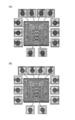
- FIG. 12A shows an enlarged photograph of the semiconductor device and the pad surface in the comparative example
- FIG. 12B shows an enlarged photograph of the semiconductor device and the pad surface in the example
- the central photograph is an enlarged photograph of the entire semiconductor device 1
- the peripheral photograph of the semiconductor device 1 is the twelve pad surfaces provided on the semiconductor device 1.
- 2 is an enlarged photograph.
- the square in the frame is the pad surface 2
- the center circle in the pad surface 2 is the initial ball 11 a
- the ring (ring) on the outside of the initial ball 11 a ) Is the crushing margin 11b.
- the crushing margin 11b is greatly generated and the initial ball 11a protrudes from the pad surface 2. It can be seen that the occurrence of the crushing allowance 11b is suppressed and fits on the pad surface 2 of the initial ball 11a.
- the diameter of the initial ball 11a bonded to the pad surface 2 provided at 12 locations in the semiconductor device 1 was measured. .
- the number of measurements was 12 times, which is the number of pad surfaces 2 provided in the semiconductor device 1.
- the diameter of the initial ball 11a is as shown in FIG.
- “X” indicates the diameter of the initial ball 11a in the X-axis direction
- “Y” indicates the diameter of the initial ball 11a in the Y-axis direction orthogonal to the X-axis.
- “Max” indicates the maximum value of each diameter
- “Min” indicates the maximum value of each diameter
- “Ave” indicates the average value of each diameter
- “ ⁇ ” Indicates a standard deviation (variation).
- the diameter of the initial ball 11a bonded to the pad surface 2 is smaller than that of the comparative example. That is, in the example, the crush margin 11b of the initial ball 11a by bonding is smaller than that in the comparative example. From this result, in the embodiment, by performing a scrubbing operation to rotate the capillary 12 in a spiral shape, when the initial ball 11a is bonded to the pad surface 2, the occurrence of the crushing margin 11b of the initial ball 11a can be suppressed to a small value. I understood that I could do it.
- FIG. 14 (a) shows an enlarged photograph of the lead surface in the comparative example
- FIG. 14 (b) shows an enlarged photograph of the lead surface in the example.
- 14A and 14B each photograph is an enlarged photograph of the lead surface 4 provided around the semiconductor device 1.
- the thick strip-shaped thing extended diagonally up and down, right and left is the lead surface 4, and the circular arc of the center of the lead surface 4 is an indentation of the capillary 12, and it extends along the lead surface 4 from this indentation.
- the thing is the bonding wire 11.
- the indentation generated when the capillary 12 is brought into pressure contact with the lead surface 4 is unclear.
- the bonding wire 11 is easily cut because the indentation is clearly generated.
- the verification of the tensile strength of the bonding wire 11 was performed by measuring the tensile strength of the bonding wire 11 fixed to each lead surface 4 provided at 12 locations in the semiconductor device 1. The number of measurements was 12 times, which is the number of lead surfaces 4 provided in the semiconductor device 1.
- the tensile strength of the bonding wire 11 was as shown in FIG.
- “crimp width” indicates the width of the bonding wire 11 that is crimped to the lead surface 4
- “tensile strength” refers to the tensile strength of the bonding wire 11 that is crimped to the lead surface 4. Is shown. “Max” indicates the maximum value of each diameter, “Min” indicates the maximum value of each diameter, “Ave” indicates the average value of each diameter, and “ ⁇ ” Indicates a standard deviation (variation).
- the tensile strength is almost the same in the example and the comparative example. From this result, in the embodiment, by performing a scrubbing operation to rotate the capillary 12 in a spiral shape, the cutting property of the bonding wire 11 is hardly reduced without substantially reducing the tensile strength of the bonding wire 11 fixed to the lead surface 4. It was found that can be improved.
- the capillary 12 is rotated.
- the pad surfaces 2 and 8 and the initial ball 11 a are rubbed in a state of being in pressure contact, so that the initial ball 11 a is fixed to the pad surfaces 2 and 8.
- the force applied to the initial ball 11a can be converged toward the center of rotation by rotating the capillary 12 in a spiral shape, the time and distance at which the pad surfaces 2, 8 and the initial ball 11a are rubbed together.
- the capillary 12 is rotated in a spiral shape while increasing the diameter, and then the capillary 12 is rotated in a spiral shape while reducing the diameter.
- the bonding wire 11 leads. While being fixed to the surface 4, the bonding wire 11 is sandwiched between the capillary 12 and the lead surface 4 and cut. Then, by rotating the capillary 12 in a spiral shape, the capillary 12 is rubbed in a spiral shape while being in pressure contact with the lead surface 4. Cutting property can be improved.
- the capillary 12 is rotated in a spiral shape while increasing the diameter, and then the capillary 12 is rotated in a spiral shape while reducing the diameter.
- the displacement between the position where the capillary 12 is in pressure contact with the lead surface 4 and the position of the indentation of the capillary 12 generated on the lead surface 4 when the capillary 12 is in pressure contact is reduced.
- the scrubbing operation is described as rotating the capillary 12 in a simple spiral shape, but the pad surfaces 2 and 8 and the lead surface 4 are formed in a strip shape (linear shape) with a predetermined width.
- the capillary 12 may be rotated in a spiral shape that is flat along the extending direction of the pad surfaces 2, 8 and the lead surface 4 as shown in FIGS. 16 and 17. .
- FIG. 16A is a diagram showing a movement trajectory when the capillary is rotated in a spiral shape that is flat in an oblique direction
- FIG. 16B is an X-axis linear motor and a Y-axis in the case of FIG. It is the figure which showed the command position for driving a linear motor.
- FIG. 17A is a diagram showing a movement locus when the capillary is rotated in a spiral shape flattened in the left-right direction.
- FIG. 17B is a diagram showing command positions for driving the X-axis linear motor and the Y-axis linear motor in the case of FIG.
- the capillaries 12 are rotated in a spiral shape along the extending direction of the pad surfaces 2 and 8, so that they are fixed to the pad surfaces 2 and 8.
- the shape of the initial ball 11a can be adapted to the shape of the pad surface. For this reason, it is possible to increase the bonding accuracy even for the pad surfaces 2 and 8 extending in an arbitrary direction.
- the capillary 12 is rotated in a flat spiral shape along the extending direction of the lead surface 4, so that the shape of the indentation of the capillary 12 formed on the lead surface 4 is formed. Can be adapted to the shape of the lead surface 4. For this reason, it is possible to improve the bonding accuracy even for the lead surface 4 extending in an arbitrary direction.
- the scrubbing operation is described as the capillary 12 is rotated three times in a spiral shape.
- the capillary 12 may be rotated any number of times, and the rotation number and the maximum diameter when rotating while expanding the diameter.
- the number of rotations and the number of rotations when rotating while reducing the diameter are not particularly limited.
- the rotation speed at the maximum diameter is preferably only one rotation in order to prevent the collapse allowance 11b of the initial ball 11a from expanding.
- the present invention is applicable to a bonding apparatus that performs bonding on a bonding target such as a semiconductor device.
- SYMBOLS 1 ... Semiconductor device, 2 ... Pad surface, 3 ... Substrate, 4 ... Lead surface, 6 ... Substrate, 7 ... Semiconductor device, 8 ... Pad surface, 10 ... Wire bonding apparatus, 11 ... Bonding wire, 11a ... Initial ball, 11b ... Crushing allowance, 12 ... capillary, 13 ... ultrasonic horn, 14 ... bonding arm, 15 ... bonding head, 16 ... arm drive motor, 17 ... bonding stage, 18 ... moving mechanism, 18a ... X-axis linear motor, 18b ... Y Axis linear motor, 20 ... control unit, 21 ... arm drive motor I / F, 22 ...
- ultrasonic horn I / F 23 ... X-axis linear motor I / F, 24 ... Y-axis linear motor I / F, 25 ... input , 26 ... output unit, 27 ... memory, 28 ... CPU, 30 ... bump bonding apparatus, 40 ... control unit, O ... reference position.
Landscapes
- Engineering & Computer Science (AREA)
- Mechanical Engineering (AREA)
- Wire Bonding (AREA)
Abstract
パッド面にボンディングする場合に、イニシャルボールの潰れ代を小さくしてボンディング精度を向上させ、リード面にボンディングする場合に、リード面に固着されたボンディングワイヤの切断性を向上させることができる。 パッド面2にイニシャルボール11aをボンディングする第1ボンディング工程において、イニシャルボール11aをパッド面2に加圧接触した状態で、超音波振動を印加するとともに、キャピラリ12を渦巻状に回転させるスクラブ動作を行う。また、ボンディングワイヤ11をリード面4にボンディングする第2ボンディング工程において、キャピラリ12及びボンディングワイヤ11をリード面4に加圧接触した状態で、超音波振動を印加するとともに、キャピラリ12を渦巻状に回転させるスクラブ動作を行う。
Description
本発明は、ボンディング対象にボンディングを行う半導体装置の製造方法およびボンディング装置に関する。
一般に、ワイヤボンディングでは、キャピラリから繰り出されるボンディングワイヤの先端にイニシャルボールを形成し、このイニシャルボールを半導体装置のパッド面に加圧接触させた状態で超音波振動を印加することで、イニシャルボールをパッド面に固着させる第1ボンディングを行っている。その後、キャピラリからボンディングワイヤを繰り出してワイヤループを形成し、このボンディングワイヤとキャピラリとを基板のリード面に加圧接触させることで、ボンディングワイヤをリード面に固着させるとともにボンディングワイヤを切断する第2ボンディングを行っている。
ところが、ボンディングステージに載置される基板がぐらつくなど基板が不安定な状態にあると、第1ボンディングの際は、イニシャルボールがパッド面に確実に固着されない場合があり、第2ボンディングの際は、ボンディングワイヤが切断できない場合があるという問題があった。
そこで、特許文献1に記載された技術では、ボンディングを行う際にキャピラリが取り付けられるXYテーブルをXY方向に移動させるスクラブ動作を行わせることで、イニシャルボールをパッド面に擦り付けてイニシャルボールをパッド面に確実に固着させている。
しかしながら、特許文献1に記載された技術では、第1ボンディングを行う際、イニシャルボールがパッド面に固着されるものの、スクラブ動作を行う際にイニシャルボールが潰れて押し広げられるため、このイニシャルボールの潰れ代が大きくなってしまう。このため、特許文献1に記載された技術では、小さいパッド面に対して高精度にボンディングすることが困難であるとともに、隣接するパッド面間の距離であるパッドピッチを小さくすることができないという問題があった。
なお、第2ボンディングの際のボンディングワイヤの切断性については、特許文献1に記載された技術でも解決されていない。
そこで、本発明は、半導体装置のパッド面にイニシャルボールをボンディングする場合に、イニシャルボールの潰れ代を小さくしてボンディング精度を向上させることができる半導体装置の製造方法及びボンディング装置を提供することを目的とする。また、本発明は、基板のリード面にボンディングワイヤをボンディングする場合に、リード面に固着されたボンディングワイヤの切断性を向上させることができる半導体装置の製造方法及びボンディング装置を提供することを目的とする。
本発明に係る半導体装置の製造方法は、パッド面が設けられたボンディング対象が載置されるボンディングステージと、先端にイニシャルボールが形成されたボンディングワイヤが挿通されるキャピラリと、ボンディングステージに載置されたボンディング対象のパッド面にイニシャルボールを加圧接触させる加圧接触手段と、パッド面にイニシャルボールが加圧接触されている際に、イニシャルボールの加圧方向と直交する方向においてキャピラリを渦巻状に回転させるスクラブ手段と、を有する制御部と、を含むボンディング装置を用意する工程と、ボンディング装置の制御部の指令に基づく加圧接触手段により、ボンディングステージに載置されたボンディング対象のパッド面に、キャピラリに挿通されたボンディングワイヤの先端に形成されたイニシャルボールを加圧接触させる加圧接触工程と、ボンディング装置の制御部の指令に基づくスクラブ手段により、パッド面にイニシャルボールが加圧接触されている際に、イニシャルボールの加圧方向と直交する方向においてキャピラリを渦巻状に回転させるスクラブ工程と、を含む。
本発明に係る半導体装置の製造方法によれば、ボンディング対象のパッド面にイニシャルボールが加圧接触されると、キャピラリを回転させることで、パッド面とイニシャルボールとが加圧接触された状態で擦り合わされるため、パッド面にイニシャルボールが固着される。このとき、キャピラリを渦巻状に回転させることで、イニシャルボールに加えられる力を回転中心方向に収束させることができるため、パッド面とイニシャルボールとが擦り合わされる時間及び距離を十分に確保しながら、パッド面とイニシャルボールとが最大径で擦り合わされる時間及び距離を低減させることができる。これにより、イニシャルボールの潰れ代を減らすことができるため、ボンディングの高精度化を図ることができるとともに、パッド面間の距離であるパッドピッチを小さくすることができる。
この場合、上記スクラブ工程は、イニシャルボールがパッド面に接触した位置を基準位置として、この基準位置から径を拡大しながらキャピラリを渦巻状に回転させた後、径を縮小しながらキャピラリを渦巻状に回転させて基準位置に戻すことが好ましい。この半導体装置の製造方法によれば、イニシャルボールがパッド面に接触した位置を基準位置として、径を拡大しながらキャピラリを渦巻状に回転させた後、径を縮小しながらキャピラリを渦巻状に回転させて基準位置に戻すことで、イニシャルボールをパッド面に加圧接触させる位置とイニシャルボールがパッド面に固着する位置とのズレを低減させることができる。これにより、ボンディングの更なる高精度化を図ることができ、パッド面間の距離であるパッドピッチをより小さくすることができる。
そして、上記スクラブ工程は、パッド面が延在している場合、パッド面の延在方向に沿って扁平した渦巻状にキャピラリを回転させることが好ましい。この半導体装置の製造方法によれば、パッド面の延在方向に沿って扁平した渦巻状にキャピラリを回転させるため、パッド面に固着されるイニシャルボールの形状をパッド面の形状に適合させることができる。このため、任意の方向に延びるパッド面に対しても、ボンディングの高精度化を図ることができる。
本発明に係るボンディング装置は、パッド面が設けられたボンディング対象が載置されるボンディングステージと、先端にイニシャルボールが形成されたボンディングワイヤが挿通されるキャピラリと、ボンディングステージに載置されたボンディング対象のパッド面にイニシャルボールを加圧接触させる加圧接触手段と、パッド面にイニシャルボールが加圧接触されている際に、イニシャルボールの加圧方向と直交する方向においてキャピラリを渦巻状に回転させるスクラブ手段と、を有する制御部と、を含む。
本発明に係るボンディング装置によれば、ボンディング対象のパッド面にイニシャルボールが加圧接触されると、キャピラリを回転させることで、パッド面とイニシャルボールとが加圧接触された状態で擦り合わされるため、パッド面にイニシャルボールが固着される。このとき、キャピラリを渦巻状に回転させることで、イニシャルボールに加えられる力を回転中心方向に収束させることができるため、パッド面とイニシャルボールとが擦り合わされる時間及び距離を十分に確保しながら、パッド面とイニシャルボールとが最大径で擦り合わされる時間及び距離を低減させることができる。これにより、キャピラリを移動させることにより発生するイニシャルボールの潰れ代を減らすことができるため、ボンディングの高精度化を図ることができるとともに、パッド面間の距離であるパッドピッチを小さくすることができる。
本発明に係る半導体装置の製造方法は、リード面が設けられたボンディング対象が載置されるボンディングステージと、ボンディングワイヤが挿通されるキャピラリと、ボンディングステージに載置されたボンディング対象のリード面に、キャピラリ及びこのキャピラリに挿通されたボンディングワイヤを加圧接触させる加圧接触手段と、リード面にキャピラリが加圧接触されている際に、キャピラリの加圧方向と直交する方向においてキャピラリを渦巻状に回転させるスクラブ手段と、を有する制御部と、を含むボンディング装置を用意する工程と、ボンディング装置の制御部の指令に基づく加圧接触手段により、ボンディングステージに載置されたボンディング対象のリード面に、ボンディングワイヤが挿通されたキャピラリ及びこのキャピラリに挿通されたボンディングワイヤを加圧接触させる加圧接触工程と、ボンディング装置の制御部の指令に基づくスクラブ手段により、リード面にキャピラリが加圧接触されている際に、キャピラリの加圧方向と直交する方向においてキャピラリを渦巻状に回転させるスクラブ工程と、を含む。
本発明に係る半導体装置の製造方法によれば、ボンディング対象のリード面にキャピラリ及びこのキャピラリに挿通されたボンディングワイヤが加圧接触されると、ボンディングワイヤがリード面に固着されるとともに、このボンディングワイヤがキャピラリとリード面との間に挟まれて切断される。そして、キャピラリを渦巻状に回転させることで、キャピラリがリード面に加圧接触された状態で渦巻状に擦り合わされるため、ボンディングワイヤの切断ミスを低減して、ボンディングワイヤの切断性を向上させることができる。
この場合、上記スクラブ工程は、キャピラリがリード面に接触した位置を基準位置として、この基準位置から径を拡大しながらキャピラリを渦巻状に回転させた後、径を縮小しながらキャピラリを渦巻状に回転させて基準位置に戻すことが好ましい。この半導体装置の製造方法によれば、キャピラリ及びボンディングワイヤがリード面に接触した位置を基準位置として、径を拡大しながらキャピラリを渦巻状に回転させた後、径を縮小しながらキャピラリを渦巻状に回転させて基準位置に戻すことで、キャピラリがリード面に加圧接触する位置と、キャピラリが加圧接触することによりリード面に発生するキャピラリの圧痕の位置とのズレを低減させることができる。これにより、ボンディングの更なる高精度化を図ることができ、リード面間の距離であるリードピッチをより小さくすることができる。
そして、上記スクラブ工程は、リード面が延在している場合、リード面の延在方向に沿って扁平した渦巻状にキャピラリを回転させることが好ましい。この半導体装置の製造方法によれば、リード面の延在方向に沿って扁平した渦巻状にキャピラリを回転させるため、リード面に形成されるキャピラリの圧痕の形状をリード面の形状に適合させることができる。このため、任意の方向に延びるリード面に対しても、ボンディングの高精度化を図ることができる。
本発明に係るボンディング装置は、リード面が設けられたボンディング対象が載置されるボンディングステージと、ボンディングワイヤが挿通されるキャピラリと、ボンディングステージに載置されたボンディング対象のリード面に、キャピラリ及びこのキャピラリに挿通されたボンディングワイヤを加圧接触させる加圧接触手段と、リード面にキャピラリが加圧接触されている際に、キャピラリの加圧方向と直交する方向においてキャピラリを渦巻状に回転させるスクラブ手段と、を有する制御部と、を含む。
本発明に係るボンディング装置によれば、ボンディング対象のリード面にキャピラリ及びこのキャピラリに挿通されたボンディングワイヤが加圧接触されると、ボンディングワイヤがリード面に固着されるとともに、このボンディングワイヤがキャピラリとリード面との間に挟まれて切断される。そして、ボンディング対象が載置されたキャピラリを渦巻状に回転させることで、キャピラリがリード面に加圧接触された状態で渦巻状に擦り合わされるため、ボンディングワイヤの切断ミスを低減して、ボンディングワイヤの切断性を向上させることができる。
本発明によれば、半導体装置のパッド面にイニシャルボールをボンディングする場合に、イニシャルボールの潰れ代を小さくしてボンディング精度を向上させることができる。また、本発明によれば、基板のリード面にボンディングワイヤをボンディングする場合に、リード面に固着されたボンディングワイヤの切断性を向上させることができる。
以下、図面を参照して、本発明に係る半導体装置の製造方法及びボンディング装置の好適な実施形態について詳細に説明する。第一の実施形態は、本発明をワイヤボンディング装置に適用したものであり、第二の実施形態は、本発明をバンプボンディング装置に適用したものである。なお、全図中、同一又は相当部分には同一符号を付すこととする。
[第1実施形態]
図1は、第1の実施形態に係るワイヤボンディング装置の一例を示した図である。図1に示すように、第1の実施形態に係るワイヤボンディング装置10は、キャピラリ12に挿通されたボンディングワイヤ11を用いてワイヤボンディングすることにより、半導体装置1に設けられたパッド面2と、この半導体装置1がボンディングされた基板3に設けられたリード面4とを、電気的に連結するものである。このため、ワイヤボンディング装置10は、ボンディングワイヤ11が挿通されるキャピラリ12と、キャピラリ12を保持するボンディングヘッド15と、ボンディングヘッド15を回転(揺動)させるアーム駆動モータ16と、ボンディング対象の基板3が載置されるボンディングステージ17と、ボンディングヘッド15を水平方向であるX軸方向及びY軸方向に移動させるXY移動機構18と、ワイヤボンディング装置10を統括的に制御する制御部20と、を備えている。
図1は、第1の実施形態に係るワイヤボンディング装置の一例を示した図である。図1に示すように、第1の実施形態に係るワイヤボンディング装置10は、キャピラリ12に挿通されたボンディングワイヤ11を用いてワイヤボンディングすることにより、半導体装置1に設けられたパッド面2と、この半導体装置1がボンディングされた基板3に設けられたリード面4とを、電気的に連結するものである。このため、ワイヤボンディング装置10は、ボンディングワイヤ11が挿通されるキャピラリ12と、キャピラリ12を保持するボンディングヘッド15と、ボンディングヘッド15を回転(揺動)させるアーム駆動モータ16と、ボンディング対象の基板3が載置されるボンディングステージ17と、ボンディングヘッド15を水平方向であるX軸方向及びY軸方向に移動させるXY移動機構18と、ワイヤボンディング装置10を統括的に制御する制御部20と、を備えている。
ボンディングヘッド15は、ボンディングヘッド15からボンディングステージ17に向けて延びており、一端にキャピラリ12を保持して他端に超音波振動を発生する振動子13aが設けられた超音波ホーン13と、超音波ホーン13を保持するボンディングアーム14とにより構成されている。このため、アーム駆動モータ16を回転駆動することで、超音波ホーン13がキャピラリ12を上下方向であるZ軸方向に移動させて、ボンディングステージ17に載置された基板3と半導体装置1とにボンディングワイヤ11をボンディングすることができる。そして、超音波ホーン13の振動子13aから超音波振動を発生させることで、ボンディングアーム14に保持されているキャピラリ12を振動させることができる。
アーム駆動モータ16は、回転(揺動)駆動することでキャピラリ12を上下方向であるZ軸方向に移動させるものである。そして、アーム駆動モータ16は、回転駆動の出力トルクを調整することで、キャピラリ12に印加する荷重を調整することができる。
XY移動機構18は、ボンディングヘッド15をX軸方向に移動させるとともに、ボンディングヘッド15をY軸方向に移動させるものである。このため、XY移動機構18には、ボンディングヘッド15をX軸方向に移動させるX軸リニアモータ18aと、ボンディングヘッド15をY軸方向に移動させるY軸リニアモータ18bとが設けられている。なお、XY移動機構18は、例えば、リニアモータ機構などにより構成されており、X軸リニアモータ18a及びY軸リニアモータ18bが回転することで、ボンディングヘッド15がX軸方向及びY軸方向に移動することが可能となる。そして、X軸リニアモータ18a及びY軸リニアモータ18bを回転させるとことで、ボンディングヘッド15がX軸方向及びY軸方向に移動することにより、キャピラリ12をX軸方向及びY軸方向に移動させることができる。
制御部20は、超音波ホーン13(振動子13a)、アーム駆動モータ16、X軸リニアモータ18a及びY軸リニアモータ18bと電気的に接続されており、超音波ホーン13、アーム駆動モータ16、X軸リニアモータ18a及びY軸リニアモータ18bを制御してワイヤボンディングを行わせるものである。
すなわち、制御部20は、キャピラリ12に挿通されたボンディングワイヤ11を半導体装置1に設けられたパッド面2にボンディングする第一ボンディング工程において、ボンディングステージ17に載置された基板3にボンディングされている半導体装置1のパッド面2に、ボンディングワイヤ11のイニシャルボール11aを加圧接触させる加圧接触機能(手段)と、パッド面2にイニシャルボール11aが加圧接触されている際に、イニシャルボール11aの加圧方向と直交する方向においてキャピラリ12を渦巻状に回転させるスクラブ機能(手段)と、を有する。また、制御部20は、パッド面2にボンディングしたボンディングワイヤ11を基板3に設けられたリード面4にボンディングする第二ボンディング工程において、ボンディングステージ17に載置された基板3のリード面4に、キャピラリ12及びキャピラリ12に挿通されたボンディングワイヤ11のイニシャルボール11aを加圧接触させる加圧接触機能(手段)と、リード面4にキャピラリ12が加圧接触されている際に、キャピラリ12の加圧方向と直交する方向においてキャピラリ12を渦巻状に回転させるスクラブ機能(手段)と、を有する。なお、この加圧接触機能及びスクラブ機能は、記憶装置などに記憶された加圧接触プログラム及びスクラブプログラムの実施により実現される。
このため、制御部20には、アーム駆動モータ16との間で信号の送受を行うアーム駆動モータI/F21と、超音波ホーン13との間で信号の送受を行う超音波ホーンI/F22と、X軸リニアモータ18aとの間で信号の送受を行うX軸リニアモータI/F23と、Y軸リニアモータ18bとの間で信号の送受を行うY軸リニアモータI/F24と、キーボードなどの入力装置であって作業者からの各種制御情報の入力を受け付ける入力部25と、モニタなどの表示装置であって制御部20の各種制御情報を表示する出力部26と、各種プログラムが格納されるメモリ27と、ボンディング制御を行うCPU28と、が設けられている。
次に、図2~図4を参照して、ワイヤボンディング装置10の処理動作について説明する。図2は、ワイヤボンディング装置を用いたボンディング方法を示すフローチャートである。図3は、図2に示した第1ボンディング工程を示すフローチャートである。図4は、図2に示した第2ボンディング工程を示すフローチャートである。なお、以下に説明するワイヤボンディング装置10の処理動作は、制御部20の指令に基づく加圧接触プログラムとしての加圧接触機能やスクラブプログラムとしてのスクラブ機能などの実施により行われる。
図2に示すように、ワイヤボンディング装置10は、まず、第1ボンディング工程を行う(ステップS1)。
図3に示すように、ステップS1の第1ボンディング工程では、まず、加圧接触工程を行う(ステップS11)。加圧接触工程では、アーム駆動モータ16を回転駆動させることによりキャピラリ12を下降させる。このとき、キャピラリ12に挿通されているボンディングワイヤ11のテールには、球状のイニシャルボール11aが形成されているため、キャピラリ12を下降させることにより、イニシャルボール11aがパッド面2に当接する。そして、イニシャルボール11aがパッド面2に当接すると、アーム駆動モータ16の出力トルクを調整することで、キャピラリ12を介してイニシャルボール11aに所定の荷重を印加して、イニシャルボール11aをパッド面2に加圧接触させる。
次に、スクラブ工程を行う(ステップS12)。スクラブ工程では、イニシャルボール11aがパッド面2に加圧接触されると、ボンディングヘッド15を移動させてキャピラリ12を渦巻状に回転させるスクラブ動作を行う。なお、スクラブ動作は、イニシャルボール11aがパッド面2に加圧接触されている間に行われれば、後述する超音波振動印加工程における超音波振動の発生期間に関わらず如何なる期間に行ってもよい。
ここで、図5を参照して、ステップS12のスクラブ動作について説明する。図5(a)は、スクラブ動作を行うキャピラリの移動軌跡を示した図であり、図5(b)は、X軸リニアモータ及びY軸リニアモータを駆動させるための指令位置を示した図である。
図5(a)に示すように、スクラブ動作は、X軸リニアモータ及びY軸リニアモータを駆動させることで、ボンディングヘッド15に保持されたキャピラリ12を渦巻状に回転させて、イニシャルボール11aをパッド面2に対して渦巻状に回転させるものである。
具体的に説明すると、スクラブ動作は、イニシャルボール11aがパッド面2に接触したときの位置を基準位置(0,0)とする。そして、この基準位置から回転半径を拡大させながらキャピラリ12を渦巻状に回転させていき、この回転半径が最大になると、回転半径を縮小させながらキャピラリ12を渦巻状に回転させていき、キャピラリ12を基準位置に戻す。なお、パッド面2が35μm四方の正方形で、イニシャルボール11aが直径20μmの球状である場合、渦巻状に回転させる最大径(直径)は、約20μm程度となる。
そして、このスクラブ動作は、図5(b)に示すX軸指令位置xおよびY軸指令位置yに基づいて、制御部20がX軸リニアモータ18a及びY軸リニアモータ18bに対して駆動制御することにより行われる。
ここで、図6及び図7を参照して、図5(b)に示すX軸指令位置x及びY軸指令位置yを算出する方法について説明する。図6は、X軸の暫定指令位置とY軸の暫定指令位置とを示す図である。図7は、X軸暫定指令位置及びY軸暫定指令位置の動作割合を示す図である。
まず、図6に示すように、円動作の基本動作となる正弦波を用いて、X軸の指令位置となるX軸暫定指令位置x1とY軸の指令位置となるY軸暫定指令位置y1とを作成する。X軸暫定指令位置x1は、3周期のサインカーブを当てはめ、Y軸暫定指令位置y1は、X軸暫定指令位置x1と90°位相のずれた3周期のコサインカーブを当てはめる。
次に、図7に示すように、X軸暫定指令位置x1及びY軸暫定指令位置y1の動作割合を作成する。すなわち、図7に示す動作割合は、キャピラリ12が移動する速度比率を示している。この動作割合は、始めの1周期を0から1まで直線的に上昇し、次の1周期を1のまま維持し、最後の1周期を1から0まで直線的に下降する。これにより、キャピラリ12の移動速度は、1周期目は、速度比率0の状態からリニアに加速して速度比率1に至り、2周期目は速度比率1で一定速度となり、3周期目は、速度比率1の状態からリニアに減速して速度比率0に至り、停止状態となる。
そして、図6に示すX軸暫定指令位置x1及びY軸暫定指令位置y1に、図7に示す動作割合を合成することで、図5(b)に示すX軸指令位置x及びY軸指令位置yを算出する。
このようにして、キャピラリ12を移動させてスクラブ動作を行わせると、イニシャルボール11aとパッド面2とが擦り合わされることにより、パッド面2の表層に形成されている酸化膜(不図示)が破れて、イニシャルボール11aがパッド面2に固着される。このとき、図8に示すように、イニシャルボール11aは、パッド面2に擦り合わされて潰れて、スクラブ動作の半径方向において外方に向けて押し広げられる潰れ代11bが発生する。ところが、スクラブ動作としてキャピラリ12を渦巻状に回転させることで、キャピラリ12を最大径で回転させているときにイニシャルボール11aとパッド面2とが擦り合わされる時間及び距離が短くなるとともに、イニシャルボール11aに加えられる力を回転中心方向に収束させることができるため、潰れ代11bが広がらずにその発生が抑制される。
次に、超音波振動印加工程を行う(ステップS13)。超音波振動印加工程では、イニシャルボール11aがパッド面2に加圧接触されると、超音波ホーン13の振動子13aから超音波振動を発生させる。すると、振動子13aで発生された超音波振動は、超音波ホーン13及びキャピラリ12を介してイニシャルボール11aに伝達される。すると、イニシャルボール11aが超音波振動することにより、イニシャルボール11aとパッド面2とが微細に擦れ合い、イニシャルボール11aがリード面4に強固に固着される。
このようにして第1ボンディング工程が終了すると、図2に示すように、ワイヤループ形成工程を行う(ステップS2)。ワイヤループ形成工程では、パッド面2にイニシャルボール11aが固着されたボンディングワイヤ11をキャピラリ12から繰り出しながらワイヤループを形成し、ボンディングワイヤ11をリード面4に当接させる。
次に、第2ボンディング工程を行う(ステップS3)。
図4に示すように、ステップS3の第2ボンディング工程では、まず、加圧接触工程を行う(ステップS31)。加圧接触工程では、アーム駆動モータ16を回転駆動させることによりキャピラリ12を下降させて、ボンディングワイヤ11とキャピラリ12とをリード面4に当接させる。すなわち、アーム駆動モータ16の出力トルクを調整することで、キャピラリ12に所定の荷重を印加して、ボンディングワイヤ11がキャピラリ12で押し潰される程度に、キャピラリ12をリード面4に加圧接触させる。これにより、ボンディングワイヤ11がリード面4に固着される。
次に、スクラブ工程を行う(ステップS32)。スクラブ工程では、第1ボンディング工程(ステップS1)におけるスクラブ工程(ステップS12)と同様に、キャピラリ12を渦巻状に回転させるスクラブ動作を行う。すると、このスクラブ動作により、ボンディングワイヤ11がキャピラリ12とリード面4との間に押し潰される。
次に、超音波振動印加工程を行う(ステップS33)。超音波振動印加工程では、第1ボンディング工程(ステップS1)における超音波振動印加工程(ステップS13)と同様に、超音波ホーン13の振動子13aから超音波振動を発生させて、イニシャルボール11aに超音波振動を印加する。すると、イニシャルボール11aがリード面4に固着される。
このようにして第2ボンディング工程が終了すると、図2に示すように、ワイヤカット工程を行う(ステップS4)。ワイヤカット工程では、まず、アーム駆動モータ16を回転駆動させることによりキャピラリ12を上昇させて、所定長さだけボンディングワイヤ11をキャピラリ12から繰り出す。その後、このボンディングワイヤ11をクランプした状態(不図示)で再度キャピラリ12を上昇させることで、ボンディングワイヤ11のテールをカットする。これにより、パッド面2とリード面4とは、ワイヤループが形成されたボンディングワイヤ11により電気的に連結される。
そして、最後に、イニシャルボール形成工程を行う(ステップ5)。イニシャルボール形成工程では、ワイヤカット工程(ステップS4)においてカットされたボンディングワイヤ11のテール(先端部)に電気トーチによる放電などを行い、ボンディングワイヤ11のテールに球状のイニシャルボール11aを形成する。
[第2実施形態]
図9は、第2の実施形態に係るバンプボンディング装置の一例を示した図である。図9に示すように、第2の実施形態に係るバンプボンディング装置30は、キャピラリ12に挿通されたボンディングワイヤ11をボンディングすることにより、基板6に固着された1又は複数の半導体装置7の各々に形成されたパッド面8にバンプを形成するものである。バンプボンディング装置30は、第1の実施形態に係るワイヤボンディング装置10と比較して、ボンディング対象及びボンディング方法が異なるものの、基本的な構成は同じである。このため、バンプボンディング装置30は、ワイヤボンディング装置10と同様に、ボンディングワイヤ11が挿通されるキャピラリ12と、キャピラリを保持するボンディングヘッド15と、ボンディングヘッド15を回転(揺動)させるアーム駆動モータ16と、ボンディング対象の基板6が載置されるボンディングステージ17と、ボンディングステージ17を水平方向であるX軸方向及びY軸方向に移動させるXY移動機構18と、バンプボンディング装置30を統括的に制御する制御部40と、を備えている。そして、ボンディングヘッド15は、一端にキャピラリ12を保持して他端に超音波振動を発生する振動子13aが設けられた超音波ホーン13と、超音波ホーン13を保持するボンディングアーム14とにより構成されている。
図9は、第2の実施形態に係るバンプボンディング装置の一例を示した図である。図9に示すように、第2の実施形態に係るバンプボンディング装置30は、キャピラリ12に挿通されたボンディングワイヤ11をボンディングすることにより、基板6に固着された1又は複数の半導体装置7の各々に形成されたパッド面8にバンプを形成するものである。バンプボンディング装置30は、第1の実施形態に係るワイヤボンディング装置10と比較して、ボンディング対象及びボンディング方法が異なるものの、基本的な構成は同じである。このため、バンプボンディング装置30は、ワイヤボンディング装置10と同様に、ボンディングワイヤ11が挿通されるキャピラリ12と、キャピラリを保持するボンディングヘッド15と、ボンディングヘッド15を回転(揺動)させるアーム駆動モータ16と、ボンディング対象の基板6が載置されるボンディングステージ17と、ボンディングステージ17を水平方向であるX軸方向及びY軸方向に移動させるXY移動機構18と、バンプボンディング装置30を統括的に制御する制御部40と、を備えている。そして、ボンディングヘッド15は、一端にキャピラリ12を保持して他端に超音波振動を発生する振動子13aが設けられた超音波ホーン13と、超音波ホーン13を保持するボンディングアーム14とにより構成されている。
制御部40は、超音波ホーン13(振動子13a)、アーム駆動モータ16、X軸リニアモータ18a及びY軸リニアモータ18bと電気的に接続されており、超音波ホーン13、アーム駆動モータ16、X軸リニアモータ18a及びY軸リニアモータ18bを制御して、半導体装置7のパッド面8にバンプを形成させるものである。
すなわち、制御部40は、キャピラリ12に挿通されたボンディングワイヤ11を半導体装置7に設けられたパッド面8にボンディングするボンディング工程において、ボンディングステージ17に載置された基板6にボンディングされている半導体装置7のパッド面8に、ボンディングワイヤ11のイニシャルボール11aを加圧接触させる加圧接触機能(手段)と、パッド面8にイニシャルボール11aが加圧接触されている際に、イニシャルボール11aの加圧方向と直交する方向においてキャピラリ12を渦巻状に回転させるスクラブ機能(手段)と、を有する。
このため、制御部40には、アーム駆動モータ16との間で信号の送受を行このため、制御部40には、アーム駆動モータ16との間で信号の送受を行うアーム駆動モータI/F21と、超音波ホーン13との間で信号の送受を行う超音波ホーンI/F22と、X軸リニアモータ18aとの間で信号の送受を行うX軸リニアモータI/F23と、Y軸リニアモータ18bとの間で信号の送受を行うY軸リニアモータI/F24と、キーボードなどの入力装置であって作業者からの各種制御情報の入力を受け付ける入力部25と、モニタなどの表示装置であって制御部40の各種制御情報を表示する出力部26と、各種プログラムが格納されるメモリ27と、ボンディング制御を行うCPU28と、が設けられている。なお、この加圧接触機能及びスクラブ機能は、記憶装置などに記憶された加圧接触プログラム及びスクラブプログラムの実施により実現される。
次に、図10及び図11を参照して、バンプボンディング装置30の処理動作について説明する。図10は、バンプボンディング装置を用いたボンディング方法を示すフローチャートである。図11は、図10に示したボンディング工程を示すフローチャートである。なお、以下に説明するバンプボンディング装置30の処理動作は、制御部40の指令に基づく加圧接触プログラムとしての加圧接触機能やスクラブプログラムとしてのスクラブ機能などの実施により行われる。
図10に示すように、バンプボンディング装置30は、まず、ボンディング工程を行う(ステップS6)。
図11に示すように、ステップS6のボンディング工程では、まず、加圧接触工程を行う(ステップS61)。加圧接触工程では、第1の実施形態における加圧接触工程(ステップS11)と同様に、キャピラリ12を下降させるとともにイニシャルボール11aに所定の荷重を印加して、イニシャルボール11aをパッド面8に加圧接触させる。
次に、スクラブ工程を行う(ステップS62)。スクラブ工程では、イニシャルボール11aがパッド面8に加圧接触されると、第1の実施形態のスクラブ工程(ステップS12)と同様に、ボンディングヘッド15を移動させてキャピラリ12を渦巻状に回転させるスクラブ動作を行う。すると、このスクラブ動作により、イニシャルボール11aとパッド面8とが擦り合わされて、パッド面8の表層に形成されている酸化膜(不図示)が破れ、イニシャルボール11aがパッド面8に固着される。このとき、スクラブ動作としてキャピラリ12を渦巻状に回転させているため、キャピラリ12を最大径で回転させているときにイニシャルボール11aとパッド面8とが擦り合わされる時間及び距離が短くなるとともに、イニシャルボール11aに加えられる力を回転中心方向に収束させることができるため、潰れ代11bが広がらずにその発生が抑制される。
次に、超音波振動印加工程を行う(ステップS63)。超音波振動印加工程では、第1の実施形態における超音波振動印加工程(ステップS13)と同様に、超音波ホーン13の振動子13aから超音波振動を発生させて、イニシャルボール11aに超音波振動を印加する。
このようにしてボンディング工程が終了すると、図10に示すように、バンプ形成工程を行う(ステップS7)。バンプ形成工程では、まず、アーム駆動モータ16を回転駆動させることによりキャピラリ12を上昇させて、所定長さだけボンディングワイヤ11をキャピラリ12から繰り出す。その後、このボンディングワイヤ11をクランプした状態(不図示)で再度キャピラリ12を上昇させることで、ボンディングワイヤ11のテールをカットする。これにより、パッド面8には、パッド面8に固着されたイニシャルボール11aによりバンプが形成される。
そして、最後に、イニシャルボール形成工程を行う(ステップS8)。イニシャルボール形成工程では、第1の実施形態におけるイニシャルボール形成工程(ステップS5)と同様に、ワイヤカット工程(ステップS4)においてカットされたボンディングワイヤ11のテール(先端部)に電気トーチによる放電などを行い、ボンディングワイヤ11のテールに球状のイニシャルボール11aを形成する。
次に、本発明の実施例について説明する。
本発明の実施例として、第1の実施形態に係るワイヤボンディング装置10を用いて、ワイヤボンディングを行った。
実施例の比較例として、スクラブ工程を行わずに第1ボンディング工程及び第2ボンディング工程を行うワイヤボンディング装置を用いて、ワイヤボンディングを行った。
そして、第1ボンディング工程によりイニシャルボール11aがボンディングされた半導体装置1のパッド面2を観察することで、パッド面2に固着されたイニシャルボール11aの寸法について検証し(第1ボンディング工程の検証)、第2ボンディング工程によりボンディングワイヤ11がボンディングされた基板3のリード面4を観察することで、リード面4に固着されたボンディングワイヤ11の引張強度について検証した(第2ボンディング工程の検証)。
[第1ボンディング工程の検証]
まず、第1ボンディング工程によりパッド面2に固着されたイニシャルボール11aの寸法について検証する。
まず、第1ボンディング工程によりパッド面2に固着されたイニシャルボール11aの寸法について検証する。
第1ボンディング工程の実験条件を、
[実施例]
・超音波振動印加時間:10ms
・キャピラリに印加する荷重:130gf
・荷重を印加する時間:13ms
・スクラブ動作:渦巻スクラブ、最大径は10μm、3周回転、周波数は250Hz
[比較例]
・超音波振動印加時間:10ms
・キャピラリに印加する荷重:170gf
・荷重を印加する時間:13ms
・スクラブ動作:なし
とした。
[実施例]
・超音波振動印加時間:10ms
・キャピラリに印加する荷重:130gf
・荷重を印加する時間:13ms
・スクラブ動作:渦巻スクラブ、最大径は10μm、3周回転、周波数は250Hz
[比較例]
・超音波振動印加時間:10ms
・キャピラリに印加する荷重:170gf
・荷重を印加する時間:13ms
・スクラブ動作:なし
とした。
図12(a)は、比較例における半導体装置及びパッド面の拡大写真を示しており、図12(b)は、実施例における半導体装置及びパッド面の拡大写真を示している。図12(a)及び図12(b)において、中央の写真は、半導体装置1全体を拡大した写真であり、半導体装置1の周辺の写真は、半導体装置1に設けられた12個のパッド面2を拡大した写真である。そして、各パッド面2を拡大した写真において、枠内の正方形がパッド面2であり、パッド面2内の中央部の円がイニシャルボール11aであり、このイニシャルボール11aの外側のリング(円環)が潰れ代11bである。図12(a)と図12(b)とを対比すると明らかなように、比較例は、潰れ代11bが大きく発生してイニシャルボール11aがパッド面2からはみ出しているのに対し、実施例は、潰れ代11bの発生が抑制されてイニシャルボール11aパッド面2に収まっていることが分かる。
イニシャルボール11aの寸法の検証は、半導体装置1に12箇所設けられたパッド面2にボンディングされているイニシャルボール11aの直径(直交するX軸方向とY軸方向におけるイニシャルボールの直径)を測定した。なお、測定回数は、半導体装置1に設けられたパッド面2の個数である12回とした。
上記条件の下で実施例と比較例とを検証した結果、イニシャルボール11aの直径は図13となった。なお、図13において、“X”は、X軸方向のイニシャルボール11aの直径を示しており、“Y”は、X軸に直交するY軸方向のイニシャルボール11aの直径を示している。また、“Max”は、各直径の最大値を示しており、“Min” は、各直径の最大値を示しており、“Ave”は、各直径の平均値を示しており、“σ”は、標準偏差(ばらつき)を示している。
図13を参照すると分かるように、実施例は、比較例に対してパッド面2にボンディングされたイニシャルボール11aの直径が小さくなっている。すなわち、実施例では、比較例よりもボンディングによるイニシャルボール11aの潰れ代11bが小さくなった。この結果から、実施例では、キャピラリ12を渦巻状に回転させるスクラブ動作を行うことで、パッド面2にイニシャルボール11aをボンディングする際に、イニシャルボール11aの潰れ代11bの発生を小さく抑えることができることが分かった。
[第2ボンディング工程の検証]
次に、第2ボンディング工程によりリード面4に固着されたボンディングワイヤ11の引張強度について検証する。
次に、第2ボンディング工程によりリード面4に固着されたボンディングワイヤ11の引張強度について検証する。
第2ボンディング工程の実験条件を、
[実施例]
・超音波振動印加時間:4ms
・キャピラリに印加する荷重:50gf
・荷重を印加する時間:7ms
・スクラブ動作:渦巻スクラブ、最大径は5μm、3周回転、周波数は350Hz
[比較例]
・超音波振動印加時間:4ms
・キャピラリに印加する荷重:50gf
・荷重を印加する時間:7ms
・スクラブ動作:直線スクラブ、最大直線長さは6μm、直線3回往復移動
とした。
[実施例]
・超音波振動印加時間:4ms
・キャピラリに印加する荷重:50gf
・荷重を印加する時間:7ms
・スクラブ動作:渦巻スクラブ、最大径は5μm、3周回転、周波数は350Hz
[比較例]
・超音波振動印加時間:4ms
・キャピラリに印加する荷重:50gf
・荷重を印加する時間:7ms
・スクラブ動作:直線スクラブ、最大直線長さは6μm、直線3回往復移動
とした。
図14(a)は、比較例におけるリード面の拡大写真を示しており、図14(b)は、実施例におけるリード面の拡大写真を示している。図14(a)及び図14(b)において、各写真は、半導体装置1の周囲に設けられたリード面4を拡大した写真である。そして、各写真において、上下、左右、斜めに延びる太い短冊状のものがリード面4であり、リード面4の中央の円弧がキャピラリ12の圧痕であり、この圧痕からリード面4に沿って延びるものがボンディングワイヤ11である。図14(a)と図14(b)とを対比すると明らかなように、比較例は、キャピラリ12がリード面4に加圧接触されることにより発生する圧痕が不明瞭であるのに対し、実施例は、この圧痕が明瞭に発生しているため、ボンディングワイヤ11がより切断されやすくなっていることが分かる。
ボンディングワイヤ11の引張強度の検証は、半導体装置1に12箇所設けられた各リード面4に固着されているボンディングワイヤ11の引張強度を測定した。なお、測定回数は、半導体装置1に設けられたリード面4の個数である12回とした。
上記条件の下で実施例と比較例とを検証した結果、ボンディングワイヤ11の引張強度は図15となった。なお、図15において、“圧着幅”は、リード面4に圧着されているボンディングワイヤ11の幅を示しており、“引張強度”は、リード面4に圧着されているボンディングワイヤ11の引張強度を示している。また、“Max”は、各直径の最大値を示しており、“Min” は、各直径の最大値を示しており、“Ave”は、各直径の平均値を示しており、“σ”は、標準偏差(ばらつき)を示している。
図15を参照すると分かるように、実施例と比較例とでは、引張強度がほぼ同じ値となっている。この結果から、実施例において、キャピラリ12を渦巻状に回転させるスクラブ動作を行うことで、リード面4に固着されたボンディングワイヤ11の引張強度を殆ど低下させることなく、このボンディングワイヤ11の切断性を向上できることが分かった。
このように、上記実施形態に係るワイヤボンディング装置10及びバンプボンディング装置30によれば、半導体装置1,7のパッド面2,8にイニシャルボール11aが加圧接触されると、キャピラリ12を回転させることで、パッド面2,8とイニシャルボール11aとが加圧接触された状態で擦り合わされるため、パッド面2,8にイニシャルボール11aが固着される。このとき、キャピラリ12を渦巻状に回転させることで、イニシャルボール11aに加えられる力を回転中心方向に収束させることができるため、パッド面2,8とイニシャルボール11aとが擦り合わされる時間及び距離を十分に確保しながら、パッド面2,8とイニシャルボール11aとが最大径で擦り合わされる時間及び距離を低減させることができる。これにより、キャピラリ12を移動させることにより発生するイニシャルボール11aの潰れ代11bを減らすことができるため、ボンディングの高精度化を図ることができるとともに、パッド面2,8間の距離であるパッドピッチを小さくすることができる。
そして、イニシャルボール11aがパッド面2,8に接触した位置を基準位置として、径を拡大しながらキャピラリ12を渦巻状に回転させた後、径を縮小しながらキャピラリ12を渦巻状に回転させて基準位置に戻すことで、イニシャルボール11aをパッド面2,8に加圧接触させる位置とイニシャルボール11aがパッド面2,8に固着する位置とのズレを低減させることができる。これにより、ボンディングの更なる高精度化を図ることができ、パッド面2,8間の距離であるパッドピッチをより小さくすることができる。
また、第1の実施形態に係るワイヤボンディング装置10によれば、基板6のリード面4にキャピラリ12及びこのキャピラリ12に挿通されたボンディングワイヤ11が加圧接触されると、ボンディングワイヤ11がリード面4に固着されるとともに、このボンディングワイヤ11がキャピラリ12とリード面4との間に挟まれて切断される。そして、キャピラリ12を渦巻状に回転させることで、キャピラリ12がリード面4に加圧接触された状態で渦巻状に擦り合わされるため、ボンディングワイヤ11の切断ミスを低減して、ボンディングワイヤ11の切断性を向上させることができる。
そして、キャピラリ12及びボンディングワイヤ11がリード面4に接触した位置を基準位置として、径を拡大しながらキャピラリ12を渦巻状に回転させた後、径を縮小しながらキャピラリ12を渦巻状に回転させて基準位置に戻すことで、キャピラリ12がリード面4に加圧接触する位置と、キャピラリ12が加圧接触することによりリード面4に発生するキャピラリ12の圧痕の位置とのズレを低減させることができる。これにより、ボンディングの更なる高精度化を図ることができ、リード面4間の距離であるリードピッチをより小さくすることができる。
以上、本発明の好適な実施形態について説明したが、本発明は上記実施形態に限定されるものではない。例えば、上記実施形態において、スクラブ動作は、単純な渦巻状にキャピラリ12を回転させるものとして説明したが、パッド面2,8及びリード面4が所定幅の短冊状(線状)に形成されて所定方向に延在している場合は、図16及び図17に示すように、パッド面2,8及びリード面4の延在方向に沿って扁平した渦巻状にキャピラリ12を回転させてもよい。すなわち、パッド面2、8及びリード面4の延在方向に向けて伸長し、この延在方向に直交する方向に短縮した楕円渦巻状にキャピラリ12を回転させるものとしてもよい。図16(a)は、斜め方向に扁平した渦巻状にキャピラリを回転させるときの移動軌跡を示した図であり、図16(b)は、(a)の場合におけるX軸リニアモータ及びY軸リニアモータを駆動させるための指令位置を示した図である。図17(a)は、左右方向に扁平した渦巻状にキャピラリを回転させるときの移動軌跡を示した図である。図17(b)は、(a)の場合におけるX軸リニアモータ及びY軸リニアモータを駆動させるための指令位置を示した図である。
そして、パッド面2,8にイニシャルボール11aをボンディングする場合は、パッド面2,8の延在方向に沿って扁平した渦巻状にキャピラリ12を回転させるため、パッド面2,8に固着されるイニシャルボール11aの形状をパッド面の形状に適合させることができる。このため、任意の方向に延びるパッド面2,8に対しても、ボンディングの高精度化を図ることができる。一方、リード面4にボンディングワイヤ11をボンディングする場合は、リード面4の延在方向に沿って扁平した渦巻状にキャピラリ12を回転させるため、リード面4に形成されるキャピラリ12の圧痕の形状をリード面4の形状に適合させることができる。このため、任意の方向に延びるリード面4に対しても、ボンディングの高精度化を図ることができる。
また、上記実施形態では、スクラブ動作として、渦巻状にキャピラリ12を3回転させるものとして説明したが、如何なる回数で回転させてもよく、径を拡大させながら回転させるときの回転数、最大径での回転数、径を縮小させながら回転させるときの回転数は、何れも特に制限されない。但し、最大径での回転数は、イニシャルボール11aの潰れ代11bが拡大するのを防止するために、1回転のみとするのが好ましい。
本発明は、半導体装置などのボンディング対象にボンディングを行うボンディング装置に利用可能である。
本発明は以上説明した実施形態に限定されるものではなく、請求の範囲により規定されている本発明の技術的範囲ないし本質から逸脱することのない全ての変更及び修正を包含するものである。
1…半導体装置、2…パッド面、3…基板、4…リード面、6…基板、7…半導体装置、8…パッド面、10…ワイヤボンディング装置、11…ボンディングワイヤ、11a…イニシャルボール、11b…潰れ代、12…キャピラリ、13…超音波ホーン、14…ボンディングアーム、15…ボンディングヘッド、16…アーム駆動モータ、17…ボンディングステージ、18…移動機構、18a…X軸リニアモータ、18b…Y軸リニアモータ、20…制御部、21…アーム駆動モータI/F、22…超音波ホーンI/F、23…X軸リニアモータI/F、24…Y軸リニアモータI/F、25…入力部、26…出力部、27…メモリ、28…CPU、30…バンプボンディング装置、40…制御部、O…基準位置。
Claims (8)
- パッド面が設けられたボンディング対象が載置されるボンディングステージと、
先端にイニシャルボールが形成されたボンディングワイヤが挿通されるキャピラリと、
ボンディングステージに載置されたボンディング対象のパッド面にイニシャルボールを加圧接触させる加圧接触手段と、パッド面にイニシャルボールが加圧接触されている際に、イニシャルボールの加圧方向と直交する方向においてキャピラリを渦巻状に回転させるスクラブ手段と、を有する制御部と、
を含むボンディング装置を用意する工程と、
ボンディング装置の制御部の指令に基づく加圧接触手段により、ボンディングステージに載置されたボンディング対象のパッド面に、キャピラリに挿通されたボンディングワイヤの先端に形成されたイニシャルボールを加圧接触させる加圧接触工程と、
ボンディング装置の制御部の指令に基づくスクラブ手段により、パッド面にイニシャルボールが加圧接触されている際に、イニシャルボールの加圧方向と直交する方向においてキャピラリを渦巻状に回転させるスクラブ工程と、
を含む半導体装置の製造方法。 - スクラブ工程は、イニシャルボールがパッド面に接触した位置を基準位置として、この基準位置から径を拡大しながらキャピラリを渦巻状に回転させた後、径を縮小しながらキャピラリを渦巻状に回転させて基準位置に戻す、請求項1に記載の半導体装置の製造方法。
- スクラブ工程は、パッド面が延在している場合、パッド面の延在方向に沿って扁平した渦巻状にキャピラリを回転させる、請求項1に記載の半導体装置の製造方法。
- パッド面が設けられたボンディング対象が載置されるボンディングステージと、
先端にイニシャルボールが形成されたボンディングワイヤが挿通されるキャピラリと、
ボンディングステージに載置されたボンディング対象のパッド面にイニシャルボールを加圧接触させる加圧接触手段と、パッド面にイニシャルボールが加圧接触されている際に、イニシャルボールの加圧方向と直交する方向においてキャピラリを渦巻状に回転させるスクラブ手段と、を有する制御部と、
を含むボンディング装置。 - リード面が設けられたボンディング対象が載置されるボンディングステージと、
ボンディングワイヤが挿通されるキャピラリと、
ボンディングステージに載置されたボンディング対象のリード面に、キャピラリ及びこのキャピラリに挿通されたボンディングワイヤを加圧接触させる加圧接触手段と、リード面にキャピラリが加圧接触されている際に、キャピラリの加圧方向と直交する方向においてキャピラリを渦巻状に回転させるスクラブ手段と、を有する制御部と、
を含むボンディング装置を用意する工程と、
ボンディング装置の制御部の指令に基づく加圧接触手段により、ボンディングステージに載置されたボンディング対象のリード面に、ボンディングワイヤが挿通されたキャピラリ及びこのキャピラリに挿通されたボンディングワイヤを加圧接触させる加圧接触工程と、
ボンディング装置の制御部の指令に基づくスクラブ手段により、リード面にキャピラリが加圧接触されている際に、キャピラリの加圧方向と直交する方向においてキャピラリを渦巻状に回転させるスクラブ工程と、
を含む半導体装置の製造方法。 - スクラブ工程は、キャピラリがリード面に接触した位置を基準位置として、この基準位置から径を拡大しながらキャピラリを渦巻状に回転させた後、径を縮小しながらキャピラリを渦巻状に回転させて基準位置に戻す、請求項5に記載の半導体装置の製造方法。
- スクラブ工程は、リード面が延在している場合、リード面の延在方向に沿って扁平した渦巻状にキャピラリを回転させる、請求項5に記載の半導体装置の製造方法。
- リード面が設けられたボンディング対象が載置されるボンディングステージと、
ボンディングワイヤが挿通されるキャピラリと、
ボンディングステージに載置されたボンディング対象のリード面に、キャピラリ及びこのキャピラリに挿通されたボンディングワイヤを加圧接触させる加圧接触手段と、リード面にキャピラリが加圧接触されている際に、キャピラリの加圧方向と直交する方向においてキャピラリを渦巻状に回転させるスクラブ手段と、を有する制御部と、
を含むボンディング装置。
Priority Applications (3)
| Application Number | Priority Date | Filing Date | Title |
|---|---|---|---|
| CN201080008761.1A CN102326241B (zh) | 2009-02-23 | 2010-01-25 | 半导体装置的制造方法以及焊接装置 |
| SG2011060969A SG173828A1 (en) | 2009-02-23 | 2010-01-25 | Method for manufacturing semiconductor device, and bonding apparatus |
| US13/214,682 US8292160B2 (en) | 2009-02-23 | 2011-08-22 | Method of manufacturing semiconductor device, and bonding apparatus |
Applications Claiming Priority (2)
| Application Number | Priority Date | Filing Date | Title |
|---|---|---|---|
| JP2009039448A JP4595018B2 (ja) | 2009-02-23 | 2009-02-23 | 半導体装置の製造方法およびボンディング装置 |
| JP2009-039448 | 2009-02-23 |
Related Child Applications (1)
| Application Number | Title | Priority Date | Filing Date |
|---|---|---|---|
| US13/214,682 Continuation US8292160B2 (en) | 2009-02-23 | 2011-08-22 | Method of manufacturing semiconductor device, and bonding apparatus |
Publications (1)
| Publication Number | Publication Date |
|---|---|
| WO2010095490A1 true WO2010095490A1 (ja) | 2010-08-26 |
Family
ID=42633776
Family Applications (1)
| Application Number | Title | Priority Date | Filing Date |
|---|---|---|---|
| PCT/JP2010/050910 Ceased WO2010095490A1 (ja) | 2009-02-23 | 2010-01-25 | 半導体装置の製造方法およびボンディング装置 |
Country Status (5)
| Country | Link |
|---|---|
| US (1) | US8292160B2 (ja) |
| JP (1) | JP4595018B2 (ja) |
| CN (1) | CN102326241B (ja) |
| SG (1) | SG173828A1 (ja) |
| WO (1) | WO2010095490A1 (ja) |
Families Citing this family (15)
| Publication number | Priority date | Publication date | Assignee | Title |
|---|---|---|---|---|
| DE102011080534A1 (de) * | 2011-08-05 | 2013-02-07 | Hesse & Knipps Gmbh | Verfahren zum Ultraschallbonden |
| TWI541920B (zh) * | 2013-07-23 | 2016-07-11 | 矽品精密工業股份有限公司 | 打線結構之製法 |
| MY171264A (en) | 2014-03-28 | 2019-10-07 | Nxp Usa Inc | Wire bonding method employing two scrub settings |
| USD771168S1 (en) | 2014-10-31 | 2016-11-08 | Coorstek, Inc. | Wire bonding ceramic capillary |
| USD797826S1 (en) | 2015-02-03 | 2017-09-19 | Coorstek, Inc. | Ceramic bonding tool with textured tip |
| USD797171S1 (en) | 2015-02-03 | 2017-09-12 | Coorstek, Inc. | Ceramic bonding tool with textured tip |
| USD797172S1 (en) | 2015-02-03 | 2017-09-12 | Coorstek, Inc. | Ceramic bonding tool with textured tip |
| USD753739S1 (en) | 2015-04-17 | 2016-04-12 | Coorstek, Inc. | Wire bonding wedge tool |
| USD868123S1 (en) | 2016-12-20 | 2019-11-26 | Coorstek, Inc. | Wire bonding wedge tool |
| JP6688725B2 (ja) * | 2016-12-26 | 2020-04-28 | ルネサスエレクトロニクス株式会社 | 半導体装置の製造方法 |
| CN112437974B (zh) * | 2018-06-06 | 2025-02-14 | 德州仪器公司 | 半导体裸片的球接合附接 |
| US11205937B2 (en) * | 2018-07-18 | 2021-12-21 | Asm Technology Singapore Pte Ltd | Driving system having reduced vibration transmission |
| WO2020039566A1 (ja) * | 2018-08-23 | 2020-02-27 | 株式会社カイジョー | ワイヤボンディング方法及びワイヤボンディング装置 |
| US11901329B2 (en) * | 2019-06-17 | 2024-02-13 | Kaijo Corporation | Wire bonding method and wire bonding apparatus |
| CN117020481B (zh) * | 2023-07-14 | 2026-01-20 | 凌波微步半导体设备(常熟)有限公司 | 一种用于焊接研磨工艺的焊接方法、装置及终端设备 |
Citations (3)
| Publication number | Priority date | Publication date | Assignee | Title |
|---|---|---|---|---|
| JPH0377338A (ja) * | 1989-08-21 | 1991-04-02 | Fujitsu Ltd | ワイヤボンディング装置 |
| JPH04372146A (ja) * | 1991-06-21 | 1992-12-25 | Toshiba Corp | ワイヤボンディング装置 |
| JPH06295941A (ja) * | 1993-04-08 | 1994-10-21 | Nec Kansai Ltd | ワイヤボンディング装置 |
Family Cites Families (23)
| Publication number | Priority date | Publication date | Assignee | Title |
|---|---|---|---|---|
| US4437604A (en) * | 1982-03-15 | 1984-03-20 | Kulicke & Soffa Industries, Inc. | Method of making fine wire interconnections |
| JP2530224B2 (ja) * | 1989-05-15 | 1996-09-04 | 株式会社新川 | ワイヤボンデイング方法 |
| US5121329A (en) * | 1989-10-30 | 1992-06-09 | Stratasys, Inc. | Apparatus and method for creating three-dimensional objects |
| US5459672A (en) * | 1990-07-30 | 1995-10-17 | Hughes Aircraft Company | Electrical interconnect integrity measuring method |
| JP2748770B2 (ja) * | 1992-05-13 | 1998-05-13 | 日本電気株式会社 | ワイヤボンディング方法 |
| JP3086158B2 (ja) * | 1995-07-26 | 2000-09-11 | 株式会社日立製作所 | 超音波ボンディング方法 |
| WO1998054545A2 (en) * | 1997-05-28 | 1998-12-03 | Absolute Sensors Limited | Position transducer and method of manufacture |
| US6090183A (en) * | 1998-09-25 | 2000-07-18 | Awaji; Toshio | Method and apparatus for processing exhaust gas produced during manufacturing of semi-conductor devices |
| AU2001248586A1 (en) * | 2000-04-20 | 2001-11-07 | Elwyn Paul Michael Wakefield | Process for forming electrical/mechanical connections |
| JP3323185B2 (ja) * | 2000-06-19 | 2002-09-09 | 田中電子工業株式会社 | 半導体素子接続用金線 |
| US7077916B2 (en) * | 2002-03-11 | 2006-07-18 | Matsushita Electric Industrial Co., Ltd. | Substrate cleaning method and cleaning apparatus |
| JP4018057B2 (ja) * | 2003-03-31 | 2007-12-05 | 株式会社新川 | ボンディング装置 |
| JP2005218579A (ja) * | 2004-02-04 | 2005-08-18 | Funai Electric Co Ltd | 自走式掃除機 |
| US7259354B2 (en) * | 2004-08-04 | 2007-08-21 | Electro Scientific Industries, Inc. | Methods for processing holes by moving precisely timed laser pulses in circular and spiral trajectories |
| CN101052493A (zh) * | 2004-09-22 | 2007-10-10 | 库利克和索夫工业公司 | 用于引线接合机接合头的运动控制装置 |
| US7731078B2 (en) * | 2004-11-13 | 2010-06-08 | Stats Chippac Ltd. | Semiconductor system with fine pitch lead fingers |
| US7954446B2 (en) * | 2005-01-27 | 2011-06-07 | Trinity Industrial Corporation | Hopper for cleaning coating machine |
| US7326640B2 (en) * | 2005-07-13 | 2008-02-05 | National Chung Cheng University | Method of realizing thermosonic wire bonding between metal wires and copper pads by depositing a thin film to surface of semiconductor chip with copper pads |
| US7597231B2 (en) * | 2006-04-10 | 2009-10-06 | Small Precision Tools Inc. | Wire bonding capillary tool having multiple outer steps |
| JP4372146B2 (ja) | 2006-12-18 | 2009-11-25 | 東京都 | 管内夾雑物の捕捉装置及びその使用方法 |
| KR101484940B1 (ko) * | 2009-05-14 | 2015-01-22 | 삼성전자 주식회사 | 로봇청소기 및 그 제어방법 |
| US8181890B2 (en) * | 2009-08-13 | 2012-05-22 | Nanoworx, LLC | Articulating and rotary cleaning nozzle spray system and method |
| US7918378B1 (en) * | 2010-08-06 | 2011-04-05 | National Semiconductor Corporation | Wire bonding deflector for a wire bonder |
-
2009
- 2009-02-23 JP JP2009039448A patent/JP4595018B2/ja active Active
-
2010
- 2010-01-25 CN CN201080008761.1A patent/CN102326241B/zh active Active
- 2010-01-25 SG SG2011060969A patent/SG173828A1/en unknown
- 2010-01-25 WO PCT/JP2010/050910 patent/WO2010095490A1/ja not_active Ceased
-
2011
- 2011-08-22 US US13/214,682 patent/US8292160B2/en active Active
Patent Citations (3)
| Publication number | Priority date | Publication date | Assignee | Title |
|---|---|---|---|---|
| JPH0377338A (ja) * | 1989-08-21 | 1991-04-02 | Fujitsu Ltd | ワイヤボンディング装置 |
| JPH04372146A (ja) * | 1991-06-21 | 1992-12-25 | Toshiba Corp | ワイヤボンディング装置 |
| JPH06295941A (ja) * | 1993-04-08 | 1994-10-21 | Nec Kansai Ltd | ワイヤボンディング装置 |
Also Published As
| Publication number | Publication date |
|---|---|
| JP2010199142A (ja) | 2010-09-09 |
| CN102326241A (zh) | 2012-01-18 |
| US20110315743A1 (en) | 2011-12-29 |
| US8292160B2 (en) | 2012-10-23 |
| CN102326241B (zh) | 2014-04-02 |
| SG173828A1 (en) | 2011-09-29 |
| JP4595018B2 (ja) | 2010-12-08 |
Similar Documents
| Publication | Publication Date | Title |
|---|---|---|
| JP4595018B2 (ja) | 半導体装置の製造方法およびボンディング装置 | |
| JP4314313B1 (ja) | ボンディング装置 | |
| JP6209800B2 (ja) | 半導体装置の製造方法及びワイヤボンディング装置 | |
| US20180331637A1 (en) | Gimbal motor mechanical limiting device and gimbal thereof | |
| JP5227227B2 (ja) | 超音波接合方法及びその装置 | |
| JP2010199142A5 (ja) | ||
| WO2018110417A1 (ja) | ワイヤボンディング装置及びワイヤボンディング方法 | |
| JP4531084B2 (ja) | ボンディング装置及びボンディング方法 | |
| JP2011171429A (ja) | 布線装置、超音波接合装置、超音波溶着装置 | |
| JP3942738B2 (ja) | バンプ接合装置及び方法、並びに半導体部品製造装置 | |
| JP6986561B2 (ja) | ワイヤボンディング方法及びワイヤボンディング装置 | |
| JP6727747B1 (ja) | ワイヤボンディング方法及びワイヤボンディング装置 | |
| WO2008066190A1 (fr) | Procédé de soudure de fils et appareil de soudure de fils | |
| JP3274731B2 (ja) | ワイヤボンディング装置 | |
| JP4234688B2 (ja) | ボンディング方法およびボンディング装置 | |
| JP4549335B2 (ja) | バンプ接合装置 | |
| JP2725116B2 (ja) | ワイヤボンディング装置及びその方法 | |
| JP2657709B2 (ja) | ワイヤボンディング装置並びにその方法 | |
| JP2725117B2 (ja) | ワイヤボンディング装置及びその方法 | |
| JP2017168735A (ja) | ワイヤボンディング方法 | |
| JP4842109B2 (ja) | フリーエアボールの形成方法及びワイヤボンディング装置 | |
| JP3493326B2 (ja) | バンプ形成方法及び装置 | |
| JP2005268676A (ja) | 電子部品の接合装置および電子部品の接合方法 | |
| KR20070076194A (ko) | 회전식 캐필러리를 갖는 와이어 본딩 장치 및 그를 이용한와이어 본딩 방법 |
Legal Events
| Date | Code | Title | Description |
|---|---|---|---|
| WWE | Wipo information: entry into national phase |
Ref document number: 201080008761.1 Country of ref document: CN |
|
| 121 | Ep: the epo has been informed by wipo that ep was designated in this application |
Ref document number: 10743619 Country of ref document: EP Kind code of ref document: A1 |
|
| NENP | Non-entry into the national phase |
Ref country code: DE |
|
| 122 | Ep: pct application non-entry in european phase |
Ref document number: 10743619 Country of ref document: EP Kind code of ref document: A1 |