WO2010089988A1 - 半導体装置 - Google Patents
半導体装置 Download PDFInfo
- Publication number
- WO2010089988A1 WO2010089988A1 PCT/JP2010/000593 JP2010000593W WO2010089988A1 WO 2010089988 A1 WO2010089988 A1 WO 2010089988A1 JP 2010000593 W JP2010000593 W JP 2010000593W WO 2010089988 A1 WO2010089988 A1 WO 2010089988A1
- Authority
- WO
- WIPO (PCT)
- Prior art keywords
- tft
- semiconductor
- silicon film
- semiconductor device
- film
- Prior art date
- Legal status (The legal status is an assumption and is not a legal conclusion. Google has not performed a legal analysis and makes no representation as to the accuracy of the status listed.)
- Ceased
Links
Images













Classifications
-
- G—PHYSICS
- G02—OPTICS
- G02F—OPTICAL DEVICES OR ARRANGEMENTS FOR THE CONTROL OF LIGHT BY MODIFICATION OF THE OPTICAL PROPERTIES OF THE MEDIA OF THE ELEMENTS INVOLVED THEREIN; NON-LINEAR OPTICS; FREQUENCY-CHANGING OF LIGHT; OPTICAL LOGIC ELEMENTS; OPTICAL ANALOGUE/DIGITAL CONVERTERS
- G02F1/00—Devices or arrangements for the control of the intensity, colour, phase, polarisation or direction of light arriving from an independent light source, e.g. switching, gating or modulating; Non-linear optics
- G02F1/01—Devices or arrangements for the control of the intensity, colour, phase, polarisation or direction of light arriving from an independent light source, e.g. switching, gating or modulating; Non-linear optics for the control of the intensity, phase, polarisation or colour
- G02F1/13—Devices or arrangements for the control of the intensity, colour, phase, polarisation or direction of light arriving from an independent light source, e.g. switching, gating or modulating; Non-linear optics for the control of the intensity, phase, polarisation or colour based on liquid crystals, e.g. single liquid crystal display cells
- G02F1/133—Constructional arrangements; Operation of liquid crystal cells; Circuit arrangements
- G02F1/1333—Constructional arrangements; Manufacturing methods
- G02F1/1345—Conductors connecting electrodes to cell terminals
- G02F1/13454—Drivers integrated on the active matrix substrate
-
- C—CHEMISTRY; METALLURGY
- C23—COATING METALLIC MATERIAL; COATING MATERIAL WITH METALLIC MATERIAL; CHEMICAL SURFACE TREATMENT; DIFFUSION TREATMENT OF METALLIC MATERIAL; COATING BY VACUUM EVAPORATION, BY SPUTTERING, BY ION IMPLANTATION OR BY CHEMICAL VAPOUR DEPOSITION, IN GENERAL; INHIBITING CORROSION OF METALLIC MATERIAL OR INCRUSTATION IN GENERAL
- C23F—NON-MECHANICAL REMOVAL OF METALLIC MATERIAL FROM SURFACE; INHIBITING CORROSION OF METALLIC MATERIAL OR INCRUSTATION IN GENERAL; MULTI-STEP PROCESSES FOR SURFACE TREATMENT OF METALLIC MATERIAL INVOLVING AT LEAST ONE PROCESS PROVIDED FOR IN CLASS C23 AND AT LEAST ONE PROCESS COVERED BY SUBCLASS C21D OR C22F OR CLASS C25
- C23F1/00—Etching metallic material by chemical means
- C23F1/10—Etching compositions
- C23F1/14—Aqueous compositions
- C23F1/16—Acidic compositions
- C23F1/26—Acidic compositions for etching refractory metals
-
- H—ELECTRICITY
- H10—SEMICONDUCTOR DEVICES; ELECTRIC SOLID-STATE DEVICES NOT OTHERWISE PROVIDED FOR
- H10D—INORGANIC ELECTRIC SEMICONDUCTOR DEVICES
- H10D30/00—Field-effect transistors [FET]
- H10D30/01—Manufacture or treatment
- H10D30/021—Manufacture or treatment of FETs having insulated gates [IGFET]
- H10D30/031—Manufacture or treatment of FETs having insulated gates [IGFET] of thin-film transistors [TFT]
- H10D30/0312—Manufacture or treatment of FETs having insulated gates [IGFET] of thin-film transistors [TFT] characterised by the gate electrodes
- H10D30/0316—Manufacture or treatment of FETs having insulated gates [IGFET] of thin-film transistors [TFT] characterised by the gate electrodes of lateral bottom-gate TFTs comprising only a single gate
-
- H—ELECTRICITY
- H10—SEMICONDUCTOR DEVICES; ELECTRIC SOLID-STATE DEVICES NOT OTHERWISE PROVIDED FOR
- H10D—INORGANIC ELECTRIC SEMICONDUCTOR DEVICES
- H10D30/00—Field-effect transistors [FET]
- H10D30/01—Manufacture or treatment
- H10D30/021—Manufacture or treatment of FETs having insulated gates [IGFET]
- H10D30/031—Manufacture or treatment of FETs having insulated gates [IGFET] of thin-film transistors [TFT]
- H10D30/0321—Manufacture or treatment of FETs having insulated gates [IGFET] of thin-film transistors [TFT] comprising silicon, e.g. amorphous silicon or polysilicon
-
- H—ELECTRICITY
- H10—SEMICONDUCTOR DEVICES; ELECTRIC SOLID-STATE DEVICES NOT OTHERWISE PROVIDED FOR
- H10D—INORGANIC ELECTRIC SEMICONDUCTOR DEVICES
- H10D30/00—Field-effect transistors [FET]
- H10D30/60—Insulated-gate field-effect transistors [IGFET]
- H10D30/67—Thin-film transistors [TFT]
- H10D30/674—Thin-film transistors [TFT] characterised by the active materials
-
- H—ELECTRICITY
- H10—SEMICONDUCTOR DEVICES; ELECTRIC SOLID-STATE DEVICES NOT OTHERWISE PROVIDED FOR
- H10D—INORGANIC ELECTRIC SEMICONDUCTOR DEVICES
- H10D86/00—Integrated devices formed in or on insulating or conducting substrates, e.g. formed in silicon-on-insulator [SOI] substrates or on stainless steel or glass substrates
- H10D86/40—Integrated devices formed in or on insulating or conducting substrates, e.g. formed in silicon-on-insulator [SOI] substrates or on stainless steel or glass substrates characterised by multiple TFTs
- H10D86/421—Integrated devices formed in or on insulating or conducting substrates, e.g. formed in silicon-on-insulator [SOI] substrates or on stainless steel or glass substrates characterised by multiple TFTs having a particular composition, shape or crystalline structure of the active layer
- H10D86/425—Integrated devices formed in or on insulating or conducting substrates, e.g. formed in silicon-on-insulator [SOI] substrates or on stainless steel or glass substrates characterised by multiple TFTs having a particular composition, shape or crystalline structure of the active layer having different crystal properties in different TFTs or within an individual TFT
-
- H—ELECTRICITY
- H10—SEMICONDUCTOR DEVICES; ELECTRIC SOLID-STATE DEVICES NOT OTHERWISE PROVIDED FOR
- H10D—INORGANIC ELECTRIC SEMICONDUCTOR DEVICES
- H10D86/00—Integrated devices formed in or on insulating or conducting substrates, e.g. formed in silicon-on-insulator [SOI] substrates or on stainless steel or glass substrates
- H10D86/40—Integrated devices formed in or on insulating or conducting substrates, e.g. formed in silicon-on-insulator [SOI] substrates or on stainless steel or glass substrates characterised by multiple TFTs
- H10D86/421—Integrated devices formed in or on insulating or conducting substrates, e.g. formed in silicon-on-insulator [SOI] substrates or on stainless steel or glass substrates characterised by multiple TFTs having a particular composition, shape or crystalline structure of the active layer
- H10D86/427—Integrated devices formed in or on insulating or conducting substrates, e.g. formed in silicon-on-insulator [SOI] substrates or on stainless steel or glass substrates characterised by multiple TFTs having a particular composition, shape or crystalline structure of the active layer having different thicknesses of the semiconductor bodies in different TFTs
-
- H—ELECTRICITY
- H10—SEMICONDUCTOR DEVICES; ELECTRIC SOLID-STATE DEVICES NOT OTHERWISE PROVIDED FOR
- H10D—INORGANIC ELECTRIC SEMICONDUCTOR DEVICES
- H10D86/00—Integrated devices formed in or on insulating or conducting substrates, e.g. formed in silicon-on-insulator [SOI] substrates or on stainless steel or glass substrates
- H10D86/40—Integrated devices formed in or on insulating or conducting substrates, e.g. formed in silicon-on-insulator [SOI] substrates or on stainless steel or glass substrates characterised by multiple TFTs
- H10D86/60—Integrated devices formed in or on insulating or conducting substrates, e.g. formed in silicon-on-insulator [SOI] substrates or on stainless steel or glass substrates characterised by multiple TFTs wherein the TFTs are in active matrices
-
- H—ELECTRICITY
- H10—SEMICONDUCTOR DEVICES; ELECTRIC SOLID-STATE DEVICES NOT OTHERWISE PROVIDED FOR
- H10D—INORGANIC ELECTRIC SEMICONDUCTOR DEVICES
- H10D30/00—Field-effect transistors [FET]
- H10D30/60—Insulated-gate field-effect transistors [IGFET]
- H10D30/67—Thin-film transistors [TFT]
- H10D30/6757—Thin-film transistors [TFT] characterised by the structure of the channel, e.g. transverse or longitudinal shape or doping profile
Definitions
- the present invention relates to a semiconductor device including a thin film transistor.
- An active matrix substrate used for a liquid crystal display device or the like includes a switching element such as a thin film transistor (hereinafter, “TFT”) for each pixel.
- a switching element such as a thin film transistor (hereinafter, “TFT”) for each pixel.
- TFT thin film transistor
- amorphous silicon TFT a TFT having an amorphous silicon film as an active layer
- polycrystalline silicon TFT a TFT having a polycrystalline silicon film as an active layer
- the polycrystalline silicon TFT Since the mobility of electrons and holes in the polycrystalline silicon film is higher than that of the amorphous silicon film, the polycrystalline silicon TFT has a higher on-current than the amorphous silicon TFT and can operate at high speed. Therefore, when an active matrix substrate is formed using a polycrystalline silicon TFT, the polycrystalline silicon TFT can be used not only as a switching element but also in a peripheral circuit such as a driver. Accordingly, there is an advantage that a part or the whole of a peripheral circuit such as a driver and the display unit can be integrally formed on the same substrate. Furthermore, there is an advantage that the pixel capacity of a liquid crystal display device or the like can be charged in a shorter switching time.
- the amorphous silicon TFT is preferably used for an active matrix substrate of a device that requires a large area. Despite the lower on-current of amorphous silicon TFTs than that of polycrystalline silicon TFTs, amorphous silicon TFTs are used in many active matrix substrates of liquid crystal televisions.
- liquid crystal display devices are strongly required to have a high performance such as a driver monolithic substrate for narrow frame and cost reduction, and a built-in touch panel function. It is difficult to fully respond to
- Patent Document 1 proposes forming an active layer of a TFT using a microcrystalline silicon ( ⁇ c-Si) film. Such a TFT is referred to as a “microcrystalline silicon TFT”.
- the microcrystalline silicon film is a silicon film having microcrystalline grains therein, and the grain boundaries of the microcrystalline grains are mainly in an amorphous phase. That is, it has a mixed state of a crystal phase composed of fine crystal grains and an amorphous phase.
- the size of each microcrystal grain is smaller than the size of the crystal grain contained in the polycrystalline silicon film.
- each microcrystalline grain has a columnar shape that grows in a columnar shape from the substrate surface, for example.
- the microcrystalline silicon film can be formed only by a film forming process such as a plasma enhanced chemical vapor deposition (plasma enhanced CVD) method using silane gas diluted with hydrogen gas as a source gas.
- a film forming process such as a plasma enhanced chemical vapor deposition (plasma enhanced CVD) method using silane gas diluted with hydrogen gas as a source gas.
- plasma enhanced CVD plasma enhanced chemical vapor deposition
- silane gas diluted with hydrogen gas as a source gas diluted with hydrogen gas as a source gas.
- annealing process a process for crystallizing the amorphous silicon film by laser or heat (annealing process) after forming the amorphous silicon film using a CVD apparatus or the like is necessary.
- a microcrystalline silicon film including a basic crystal phase can be formed by a CVD apparatus or the like, so that a crystallization process using a laser or heat or a thermal annealing process can be omitted.
- the microcrystalline silicon TFT since the microcrystalline silicon film is formed with a smaller number of processes than the number of processes necessary for forming the polycrystalline silicon film, the microcrystalline silicon TFT has the same productivity as the amorphous silicon TFT, that is, the same. It can be manufactured with a moderate number of steps and cost. In addition, a microcrystalline silicon TFT can be manufactured using an apparatus for manufacturing an amorphous silicon TFT.
- the microcrystalline silicon film has higher mobility than the amorphous silicon film, by using the microcrystalline silicon film, a higher on-current than the amorphous silicon TFT can be obtained. Further, since the microcrystalline silicon film can be formed without performing a complicated process like the polycrystalline silicon film, the manufacturing cost can be reduced.
- Patent Document 1 describes that by using a microcrystalline silicon film as an active layer of a TFT, an ON current 1.5 times that of an amorphous silicon TFT can be obtained.
- Non-Patent Document 1 provides a TFT having an on / off ratio of 10 6 , a mobility of about 1 cm 2 / Vs, and a threshold value of about 5 V by using a semiconductor film made of microcrystalline silicon and amorphous silicon. It is described. This mobility is higher than the mobility of the amorphous silicon TFT.
- Patent Document 2 discloses an inverted stagger type (bottom gate structure) TFT using a microcrystalline silicon film.
- a microcrystalline silicon TFT using a microcrystalline silicon film has high mobility and on-state current.
- Such a microcrystalline silicon TFT can be used for a monolithic substrate or a thin film substrate in order to reduce the frame of a display device or reduce the cost. It is suitably used for touch panels.
- the monolithic substrate and the touch panel will be briefly described.
- an active matrix substrate in which a drive circuit is formed on a substrate has been commercialized in order to reduce the frame (panel outer shape) size, reduce costs by reducing driver ICs to be mounted, and improve the mounting yield.
- Such an active matrix substrate is called a driver monolithic substrate or a monolithic substrate.
- the monolithic substrate of Patent Document 3 includes not only TFTs that function as switching elements for pixels in the display area but also TFTs that function as switching elements in a drive circuit in the peripheral area.
- touch panels have been manufactured by attaching a resistive film type or capacitive type touch sensor module, which is manufactured separately from the display panel, to the display panel. Touch panels that have been developed are also being studied.
- Such a touch panel is manufactured using an active matrix substrate provided with a diode as a semiconductor element different from the TFT (see, for example, Patent Document 4).
- the active matrix substrate of Patent Document 4 not only a TFT but also a photodiode is provided.
- the polycrystalline silicon film of the diode is formed in the same process as the polycrystalline silicon film of the TFT, and the manufacturing cost is reduced.
- a monolithic substrate provided with a TFT having a microcrystalline silicon film having a relatively high carrier mobility as part of a semiconductor layer has been studied (for example, see Patent Document 5).
- a TFT in a display region of an active matrix substrate and having one of a source electrode and a drain electrode connected to a pixel electrode is referred to as a pixel TFT, and other TFTs (specifically, the display region)
- a TFT in a peripheral region that constitutes a driver circuit, an amplifier circuit, a charge readout circuit, or the like may be referred to as a circuit TFT.
- Patent Document 5 discloses a semiconductor device provided with a pixel TFT having a microcrystalline silicon film as a part of a semiconductor layer and a circuit TFT having an amorphous silicon film.
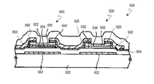
- FIG. 37 shows a semiconductor device 900 disclosed in Patent Document 5.
- the semiconductor device 900 includes a TFT 920 and a TFT 940.
- the TFT 920 is a pixel TFT
- the TFT 940 is a circuit TFT.
- the semiconductor layer 930 of the TFT 920 and the semiconductor layer 950 of the TFT 940 each have a three-layer structure.
- the layers 932, 934, and 936 included in the semiconductor layer 930 of the TFT 920 are all formed from amorphous silicon, whereas the layers 952, 954, and 956 included in the semiconductor layer 950 of the TFT 940 are mainly polycrystalline silicon, It is made of microcrystalline silicon or amorphous silicon. Therefore, the off current of the TFT 920 is low, and the on current of the TFT 940 is high.
- the manufacture of the semiconductor device 900 is performed as follows. First, gate electrodes 922 and 942 are formed over the substrate 902, and then an insulating layer 904 covering the gate electrodes 922 and 942 is deposited.
- the peripheral layer 952 is irradiated with an excimer laser to be crystallized, whereby the layer 952 is formed from the amorphous silicon film. Modification to a crystalline silicon film.
- the layer 934 on the layer 932 is formed mainly from amorphous silicon, but is polycrystalline.
- the layer 954 above the silicon layer 952 is mainly formed from microcrystalline silicon.
- layers of amorphous silicon 936 and 956 are further formed on the layers 934 and 954.
- the semiconductor device 900 including the TFT 920 and the TFT 940 having different characteristics is manufactured.
- the microcrystalline silicon TFT has a larger on-current than the amorphous silicon TFT, and the microcrystalline silicon TFT is suitably used as a circuit TFT.
- the microcrystalline silicon TFT has a high off current and cannot realize a high on / off ratio
- the microcrystalline silicon TFT is simply used as a pixel TFT, the potential of the pixel electrode is sufficiently increased due to the large off current. I can't hold it.
- the pixel electrode potential cannot be sufficiently held under driving conditions such as a high pixel potential writing interval such as in a high-temperature environment or low-frequency driving.
- a TFT 920 with a low off-current is used as the pixel TFT, and a TFT 940 with a high on-current is used as the circuit TFT.
- a TFT 940 with a high on-current is used as the circuit TFT.
- a microcrystalline silicon TFT is manufactured together with a diode
- the semiconductor layer of the diode is formed of a microcrystalline silicon film
- the light absorption rate and the photocurrent of the microcrystalline silicon film are lower than those of the amorphous silicon film.
- Such a diode does not sufficiently function as a photosensor.
- the present invention has been made in view of the above problems, and an object of the present invention is to provide a semiconductor device in which TFTs having different characteristics are easily manufactured. Another object of the present invention is to provide a semiconductor device including a TFT having a microcrystalline semiconductor film and a diode having good photoresponse characteristics.
- a semiconductor device includes a first thin film transistor and a second thin film transistor that is different from the first thin film transistor, wherein the first thin film transistor includes a gate electrode and a semiconductor layer including a microcrystalline semiconductor film. And a gate insulating layer provided between the gate electrode and the semiconductor layer.
- the second thin film transistor includes a gate electrode, a semiconductor layer including a microcrystalline semiconductor film, and the gate electrode.
- the gate insulating layer of the first thin film transistor has a thickness, a layer structure, and a dielectric constant smaller than the semiconductor layer of the first thin film transistor. Both different from the gate insulating layer of the second thin film transistor by a single point.
- the semiconductor layer of the first thin film transistor further includes an amorphous semiconductor film.
- the semiconductor layer of the second thin film transistor further includes an amorphous semiconductor film, and the amorphous semiconductor film of the first thin film transistor is thicker than the amorphous semiconductor film of the second thin film transistor.
- the thickness of the microcrystalline semiconductor film of the first thin film transistor is substantially equal to the thickness of the microcrystalline semiconductor film of the second thin film transistor.
- the thickness of the microcrystalline semiconductor film of the first thin film transistor is different from the thickness of the microcrystalline semiconductor film of the second thin film transistor.
- the gate insulating layer of the first thin film transistor is thicker than the gate insulating layer of the second thin film transistor.
- the gate insulating layer of the first thin film transistor has a multi-layer structure, and a composition of a portion of the gate insulating layer in contact with the semiconductor layer in the first thin film transistor is determined in the second thin film transistor.
- the composition of the portion of the gate insulating layer in contact with the semiconductor layer is different.
- the crystallization rate of the microcrystalline semiconductor film of the first thin film transistor is different from the crystallization rate of the microcrystalline semiconductor film of the second thin film transistor.
- a semiconductor device includes a first thin film transistor and a second thin film transistor that is different from the first thin film transistor, wherein the first thin film transistor includes a gate electrode and an amorphous semiconductor film. And a gate insulating layer provided between the gate electrode and the semiconductor layer.
- the second thin film transistor includes a gate electrode and a microcrystalline semiconductor film which does not include an amorphous semiconductor film.
- Including a semiconductor layer, and a gate insulating layer provided between the gate electrode and the semiconductor layer, and the semiconductor layer of the first thin film transistor includes a thickness, a layer structure, and a crystallization ratio. It differs from the semiconductor layer of the second thin film transistor in at least one point.
- the semiconductor device further includes a diode, and the diode includes a semiconductor layer including a microcrystalline semiconductor film and an amorphous semiconductor film.
- An active matrix substrate according to the present invention is an active matrix substrate including the semiconductor device described above, and a drain electrode of the second thin film transistor is connected to a pixel electrode.
- a semiconductor device includes a thin film transistor and a diode, and the thin film transistor includes a semiconductor layer including a microcrystalline semiconductor film, and the diode includes a microcrystalline semiconductor film and an amorphous semiconductor.
- a semiconductor layer including a film is included.
- the semiconductor layer of the thin film transistor further includes an amorphous semiconductor film.
- the amorphous semiconductor film of the diode is thicker than the amorphous semiconductor film of the thin film transistor.
- An active matrix substrate according to the present invention is an active matrix substrate including the semiconductor device described above, and the diode is provided in a display region.
- a semiconductor device including TFTs having different characteristics it is possible to easily provide a semiconductor device including TFTs having different characteristics. Further, according to the present invention, a semiconductor device including a TFT having a microcrystalline semiconductor film and a diode having high photoresponse characteristics can be provided.
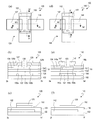
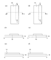
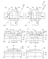
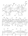
- FIG. 1 is a schematic diagram which shows 1st Embodiment of the semiconductor device by this invention, (a) is a top view of the 1st thin-film transistor in a semiconductor device, (b) and (c) are 2b-2b 'of (a), respectively. And (d) is a top view of a second thin film transistor in the semiconductor device, and (e) and (f) are respectively a line 2e-2e ′ and a line 2c-2c ′.
- FIG. 3 is a cross-sectional view taken along line 2f-2f ′.
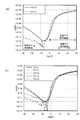
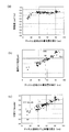
- (A) and (b) are both graphs showing the characteristics of TFT gate voltage Vgd-drain current Isd.
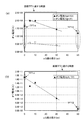
- (A) is a graph which shows the change of the on-current with respect to the change of the thickness of the amorphous silicon film in a semiconductor layer
- (b) is a graph which shows the change of the off-current with respect to the change of the thickness of the amorphous silicon film in a semiconductor layer. is there.
- (A) is a graph which shows the change of ON / OFF ratio with respect to the change of the thickness of the amorphous silicon film in a semiconductor layer
- (b) is the change of the threshold voltage with respect to the change of the thickness of the amorphous silicon film in a semiconductor layer. It is a graph which shows. It is the schematic for demonstrating the manufacturing method of the semiconductor device of 1st Embodiment.
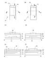
- (A)-(f) is a schematic diagram for demonstrating the manufacturing method of the semiconductor device of 1st Embodiment.
- (A)-(f) is a schematic diagram for demonstrating the manufacturing method of the semiconductor device of 1st Embodiment.
- (A)-(f) is a schematic diagram for demonstrating the manufacturing method of the semiconductor device of 1st Embodiment.
- (A)-(f) is a schematic diagram for demonstrating the manufacturing method of the semiconductor device of 1st Embodiment.
- (A)-(f) is a schematic diagram for demonstrating the manufacturing method of the semiconductor device of 1st Embodiment.
- (A)-(f) is a schematic diagram for demonstrating the manufacturing method of the semiconductor device of 1st Embodiment.
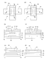
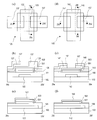
- FIG. 6 is a schematic diagram illustrating a modification of the semiconductor device of the first embodiment, (a) is a top view of a first thin film transistor in the semiconductor device, and (b) and (c) are 16b-16b ′ of (a), respectively. And (d) is a top view of a second thin film transistor in the semiconductor device, and (e) and (f) are respectively a line 16e-16e ′ of (d) and a line 16c-16c ′.
- FIG. 16 is a cross-sectional view taken along line 16f-16f ′.
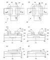
- FIG. 6A is a schematic diagram showing another modification of the semiconductor device of the first embodiment, FIG.
- FIG. 7A is a top view of a first thin film transistor in the semiconductor device
- FIGS. FIG. 17B is a cross-sectional view taken along lines 17b ′ and 17c-17c ′
- FIG. 10D is a top view of the second thin film transistor in the semiconductor device
- FIGS. 17E and 17F are 17e-17e ′ of FIG.
- FIG. 17 is a cross-sectional view taken along line 17f-17f ′.
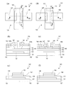
- It is a schematic diagram which shows another modification of the semiconductor device of 1st Embodiment, (a) is a top view of the 1st thin-film transistor in a semiconductor device, (b) and (c) are 18b of (a), respectively.
- FIG. 18D is a cross-sectional view taken along the lines ⁇ 18b ′ and 18c ⁇ 18c ′
- FIG. 8D is a top view of the second thin film transistor in the semiconductor device
- FIGS. FIG. 18 is a cross-sectional view taken along a line “18f-18f”.
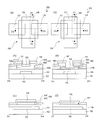
- It is a schematic diagram which shows another modification of the semiconductor device of 1st Embodiment, (a) is a top view of the 1st thin-film transistor in a semiconductor device, (b) and (c) are 19b of (a), respectively.
- FIG. 19 is a cross-sectional view taken along the lines “-19b” and 19c-19c ′.
- FIG. 6 is a schematic diagram showing a second embodiment of a semiconductor device according to the present invention, (a) is a top view of a first thin film transistor in the semiconductor device, and (b) and (c) are 20b-20b ′ of (a), respectively. And (d) is a top view of a second thin film transistor in the semiconductor device, and (e) and (f) are respectively a line 20e-20e ′ of (d) and a line 20c-20c ′.
- FIG. 20 is a cross-sectional view taken along line 20f-20f ′.
- FIG. 7 is a schematic diagram showing a semiconductor device of Comparative Example 1, (a) is a top view of a first thin film transistor in the semiconductor device, and (b) and (c) are lines 21b-21b ′ and 21c ⁇ in FIG. 21D is a cross-sectional view taken along a line 21c ′, FIG. 10D is a top view of a second thin film transistor in the semiconductor device, and FIGS. 21E and 21F are a line 21e-21e ′ and a line 21f-21f ′ in FIG. It is sectional drawing along a line. It is the schematic for demonstrating the manufacturing method of the semiconductor device of 2nd Embodiment.
- (A)-(f) is a schematic diagram for demonstrating the manufacturing method of the semiconductor device of 2nd Embodiment.
- (A)-(f) is a schematic diagram for demonstrating the manufacturing method of the semiconductor device of 2nd Embodiment.
- (A)-(f) is a schematic diagram for demonstrating the manufacturing method of the semiconductor device of 2nd Embodiment.
- (A)-(f) is a schematic diagram for demonstrating the manufacturing method of the semiconductor device of 2nd Embodiment.
- (A)-(f) is a schematic diagram for demonstrating the manufacturing method of the semiconductor device of 2nd Embodiment.
- FIG. 7A is a schematic diagram showing a modification of the semiconductor device of the second embodiment
- FIG. 9A is a top view of a first thin film transistor in the semiconductor device
- FIGS. 29B and 29C are 29b-29b ′ of FIG.
- FIG. 29 is a cross-sectional view taken along line 29f-29f ′.
- It is a schematic diagram showing a third embodiment of a semiconductor device according to the present invention, (a) is a top view of a first thin film transistor in the semiconductor device, (b) and (c) are 30b-30b ′ of (a), respectively.
- FIG. 10 is a schematic diagram illustrating a modification of the semiconductor device of the third embodiment, where (a) is a top view of a first thin film transistor in the semiconductor device, and (b) and (c) are 31b-31b ′ of (a), respectively.
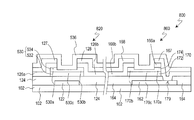
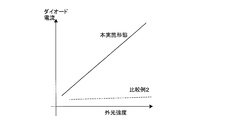
- FIG. 31 is a cross-sectional view taken along line 31f-31f ′. It is a schematic diagram which shows 4th Embodiment of the semiconductor device by this invention. It is a graph which shows the characteristic in the photodiode in the semiconductor device of 4th Embodiment and Comparative Example 2.
- (A) is a schematic diagram of the active matrix substrate provided with the semiconductor device of 4th Embodiment
- (b) is a circuit diagram which shows a liquid crystal display device provided with an active matrix substrate
- (c) is a cross section of a liquid crystal display device It is a figure
- (d) is a circuit diagram which shows another liquid crystal display device provided with an active matrix substrate.
- It is a schematic diagram which shows the 1st thin-film transistor in the modification of the semiconductor device of 4th Embodiment.
- It is a schematic diagram which shows an organic electroluminescence display provided with 5th Embodiment of the semiconductor device by this invention.
- the microcrystalline silicon film preferably has the following characteristics.
- the microcrystalline silicon film has a mixed state of a crystalline phase composed of microcrystalline grains and an amorphous phase.
- the volume ratio of the amorphous phase in the microcrystalline silicon film can be controlled in the range of 5% to 95%, for example.
- the volume ratio of the amorphous phase is preferably 5% or more and 40% or less. In this range, a good microcrystalline silicon film with few defects in the film can be obtained, so that the on / off ratio of the TFT can be improved more effectively. it can.
- Raman scattering spectrum analysis using visible light is performed on the microcrystalline silicon film, the spectrum has the highest peak at a wavelength near 520 cm ⁇ 1, which is the peak of crystalline silicon, and the peak of amorphous silicon.
- the peak heights of the amorphous silicon film near 480 cm -1 becomes 1/30 or more and 1 or less of the peak heights of the crystalline silicon film to be seen in the vicinity of 520 cm -1.
- Such a microcrystalline silicon film can be formed by a high-density plasma CVD such as a capacitively coupled plasma (CCP) method or an inductively coupled plasma (ICP) method, for example.
- a high-density plasma CVD such as a capacitively coupled plasma (CCP) method or an inductively coupled plasma (ICP) method, for example.
- CCP capacitively coupled plasma
- ICP inductively coupled plasma
- FIG. 1A to 1C are schematic enlarged cross-sectional views illustrating an amorphous silicon film, a polycrystalline silicon film, and a microcrystalline silicon film, respectively.
- the amorphous silicon film is formed from an amorphous phase 702.
- Such an amorphous silicon film is usually formed on the substrate 701 by a plasma CVD method or the like.
- the polycrystalline silicon film is composed of a plurality of crystal grains 732 separated by crystal grain boundaries 731. Further, the polycrystalline silicon film is substantially formed of polycrystalline silicon, and the volume ratio of the crystal grain boundary 731 occupying the polycrystalline semiconductor is extremely small.
- the polycrystalline silicon film can be obtained, for example, by performing a crystallization process by laser or heat on the amorphous silicon film formed on the substrate 701.
- the microcrystalline silicon film includes microcrystalline grains 733 and crystal grain boundaries 734 made of an amorphous phase.
- a thin amorphous layer (hereinafter referred to as “incubation layer”) 735 is formed on the substrate side of the microcrystalline silicon film.
- the crystal grain boundary 734 and the incubation layer 735 become the “amorphous phase” 736 of the microcrystalline silicon film, and the plurality of microcrystalline grains 733 become the “crystal phase” 737.
- each microcrystalline grain 733 extends in a column shape from the incubation layer 735 to the upper surface of the microcrystalline silicon film along the thickness direction of the microcrystalline silicon film.
- a microcrystalline silicon film can be formed using, for example, a plasma CVD method similar to the method for forming an amorphous silicon film, using a silane gas diluted with hydrogen gas as a source gas.
- the microcrystalline grains 733 in the microcrystalline silicon film are smaller than the crystal grains 732 in the polycrystalline silicon film.
- the average grain size of the microcrystalline grains 733 is 2 nm to 300 nm.
- the average grain size of the microcrystalline grains 733 is an average grain diameter in a cross section along a substantially plane direction of the substrate provided with the microcrystalline silicon film. Accordingly, since the crystal cross section of the microcrystalline grain 733 is sufficiently smaller than the size of the semiconductor element, the characteristics of the semiconductor element can be made uniform.
- the incubation layer 735 tends to grow early in the formation of the microcrystalline silicon film.
- the thickness of the incubation layer 735 is, for example, several nm although it depends on the formation conditions of the microcrystalline silicon film.
- the incubation layer 735 may be hardly seen depending on the formation conditions and the formation method of the microcrystalline silicon film, particularly when the high-density plasma CVD method is used.
- each microcrystalline grain 733 has a columnar shape extending in a substantially normal direction of the substrate 701.
- the microcrystalline silicon film can also be defined as a silicon film including columnar crystal grains extending in the normal direction of the substrate.
- the structure of the microcrystalline silicon film varies depending on the formation method and conditions, and is not limited to the illustrated structure.
- the volume fraction of the amorphous phase and the peak intensity ratio in the microcrystalline silicon film are: It is preferable to be within the above-described range, whereby a TFT having high on characteristics can be realized.
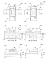
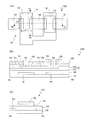
- the semiconductor device 100 of this embodiment has a plurality of TFTs 120 and TFTs 140.
- the TFT 120 and the TFT 140 are inverted staggered channel protection type TFTs.
- FIGS. 2A is a top view of the TFT 120
- FIGS. 2B and 2C are cross-sectional views of the TFT 120
- FIG. FIGS. 2B and 2C correspond to cross sections taken along lines 2b-2b 'and 2c-2c' of FIG. 2A, respectively.
- 2D shows a top view of the TFT 140
- FIGS. 2E and 2F show cross-sectional views of the TFT 140.
- FIGS. 2E and 2F correspond to cross sections taken along lines 2e-2e 'and 2f-2f' of FIG. 2D, respectively.
- the TFT 120 includes a gate electrode 122 provided on the substrate 102, a gate insulating layer 124 covering the gate electrode 122, a source electrode 127, a drain electrode 128, and a semiconductor layer 130 provided on the gate insulating layer 124.
- a channel protective layer 136 covering a part of the semiconductor layer 130.
- the semiconductor layer 130 has a source region 130a, a drain region 130b, and a channel region 130c.
- the source region 130a of the semiconductor layer 130 is electrically connected to the source electrode 127 through the contact layer 126a, and the drain region 130b of the semiconductor layer 130 is electrically connected to the drain electrode 128 through the contact layer 126b. Yes.
- the TFT 140 includes a gate electrode 142 provided over the substrate 102, a gate insulating layer 144 covering the gate electrode 142, a source electrode 147, a drain electrode 148, and a semiconductor layer 150 provided over the gate insulating layer 144. And a channel protective layer 156 that covers part of the semiconductor layer 150.
- the semiconductor layer 150 includes a source region 150a, a drain region 150b, and a channel region 150c.
- the source region 150a of the semiconductor layer 150 is electrically connected to the source electrode 147 through the contact layer 146a, and the drain region 150b of the semiconductor layer 150 is electrically connected to the drain electrode 148 through the contact layer 146b. Yes.
- the thickness of the gate insulating layers 124 and 144 is approximately 400 nm regardless of whether or not they are on the gate electrodes 122 and 142, and the gate insulating layers 124 and 144 are formed of silicon nitride (SiN x ). .
- the channel protective layers 136 and 156 have a thickness of 150 nm, and the channel protective layers 136 and 156 are also formed of silicon nitride (SiN x ).
- the width of the source electrode 127 is substantially equal to the width of the drain electrode 128, and the width of the source electrode 147 is substantially equal to the width of the drain electrode 148.
- the gate electrode 122 and the gate electrode 142 are formed in the same process, and the gate electrode 122 and the gate electrode 142 are formed of the same material (for example, molybdenum (Mo)).
- Mo molybdenum
- the channel regions 130c and 150c of the semiconductor layers 130 and 150 are covered with channel protection layers 136 and 156, respectively.
- the contact layers 126a and 126b and the contact layers 146a and 146b are formed in the same process, and the contact layers 126a and 126b and the contact layers 146a and 146b are formed of the same material (for example, silicon doped with phosphorus).
- the source electrodes 127 and 147 and the drain electrodes 128 and 148 are formed in the same process, and the source electrodes 127 and 147 and the drain electrodes 128 and 148 are formed of the same material (for example, molybdenum (Mo)). .
- the semiconductor layer 130 and the semiconductor layer 150 have a multilayer structure.
- the semiconductor layer 130 includes a microcrystalline semiconductor film 132 provided over the gate insulating layer 124 and an amorphous semiconductor film 134 provided over the microcrystalline semiconductor film 132 and the channel protective layer 136.
- the semiconductor layer 150 includes a microcrystalline semiconductor film 152 provided over the gate insulating layer 144 and an amorphous semiconductor film 154 provided over the microcrystalline semiconductor film 152 and the channel protective layer 156.
- a mode in which a microcrystalline silicon film is used as an example of a microcrystalline semiconductor film and an amorphous silicon film is used as an example of an amorphous semiconductor film will be described.
- the microcrystalline silicon films 132 and 152 are formed of the same material (for example, microcrystalline silicon), and the amorphous silicon films 134 and 154 are formed of the same material (for example, amorphous silicon).
- the contact layers 126a and 126b are provided on the microcrystalline silicon film 132 with the amorphous silicon film 134 interposed therebetween. Similarly, the contact layers 146a and 146b are provided over the microcrystalline silicon film 152 with the amorphous silicon film 154 interposed therebetween.
- the semiconductor layers 130 and 150 located on the gate electrodes 122 and 142 determine the basic characteristics of the TFTs 120 and 140.
- the semiconductor layer 150 of the TFT 140 is different from the semiconductor layer 130 of the TFT 120.
- the thickness of the microcrystalline silicon film 152 of the TFT 140 is substantially equal to the microcrystalline silicon film 132 of the TFT 120, but the amorphous silicon film 154 of the TFT 140 is thinner than the amorphous silicon film 134 of the TFT 120.
- the microcrystalline silicon films 132 and 152 have a thickness of 50 nm
- the amorphous silicon film 134 has a thickness of 30 nm
- the amorphous silicon film 154 has a thickness of 10 nm.
- the thickness of the amorphous silicon film 154 of the semiconductor layer 150 is different from that of the amorphous silicon film 134 of the semiconductor layer 130.
- the thickness of the microcrystalline silicon films 132 and 152 is preferably 20 nm to 60 nm.
- the thickness of the microcrystalline silicon film is less than 20 nm, the mobility is lowered and the on-characteristic of the TFT is lowered.
- the thickness of the microcrystalline silicon film exceeds 60 nm, the off-current of the TFT increases and the on / off ratio decreases.
- the characteristics of the TFT 120 are different from those of the TFT 140. Specifically, when the gate voltages are equal, the on-current of the TFT 140 is larger than the on-current of the TFT 120. Further, when the gate voltages are equal, the off current of the TFT 120 is smaller than the off current of the TFT 140. Focusing on the ratio of on-current to off-current (on / off ratio), the on / off ratio of the TFT 120 is larger than that of the TFT 140.
- the TFT 120 may be referred to as a first thin film transistor, and the TFT 140 may be referred to as a second thin film transistor.
- a region where the TFT 120 is provided may be referred to as a first region
- a region where the TFT 140 is provided may be referred to as a second region.
- Such a semiconductor device 100 is preferably used for manufacturing an active matrix substrate of a display device.
- the TFT 140 having a high on-current is preferably used as a circuit TFT in the peripheral region, and the TFT 120 having a low off-current is preferably used as a pixel TFT in the display region.
- FIG. 3A shows the characteristics of the gate voltage Vgd-drain current Isd of the TFT-A and TFT-B at room temperature (approximately 23 ° C.) when the source voltage Vsd is 10V.
- the following TFT characteristics are characteristics measured in a dark room at room temperature.
- TFT-A and TFT-B have the same configuration as the TFTs 120 and 140 described above except that the semiconductor layers are different.
- the TFT-A has only a microcrystalline silicon film as a semiconductor layer, and the thickness of the microcrystalline silicon film is 50 nm.
- the TFT-B has only an amorphous silicon film as a semiconductor layer, and the thickness of the amorphous silicon film is 50 nm.
- the semiconductor layer is in contact with the gate insulating layer and directly in contact with the contact layer.
- the channel length corresponding to the width of the channel protective layer in the direction connecting the source electrode and the drain electrode is 10 ⁇ m
- the channel width corresponding to the width of the source electrode is 20 ⁇ m.
- the width of the source electrode is substantially equal to the width of the drain electrode.
- the gate voltage Vgd and the source voltage Vsd indicate the potential of the gate electrode and the source electrode with respect to the potential of the drain electrode, respectively, and the drain current Isd indicates the current between the source and drain.
- the drain current Isd is minimized in both TFT-A and TFT-B.
- the gate voltage Vgd is approximately in the range of Vgd ⁇ 8V
- the drain current Isd of the TFT-A increases remarkably as the gate voltage Vgd decreases, but the increase in the TFT-B is smaller than that in the TFT-A.
- the off-current of TFT-A is larger than the off-current of TFT-B.
- the threshold value (threshold voltage) of TFT-A is higher than that of TFT-B, but the mobility of TFT-A is higher than that of TFT-B. Therefore, in the range of gate voltage Vgd> 10V, TFT-A The drain current Isd of A is larger than that of TFT-B. From the above, when the ranges of the gate voltages Vgd ⁇ 8 V and Vgd> 10 V are used as the TFT off-range and on-range, the on-current and off-current of the TFT-A are both larger than those of the TFT-B.
- the gate voltage Vgd is held at a value higher than zero when the TFT is on, and the gate voltage Vgd is held at a value lower than zero as the TFT is off. Transition. As described above, the gate voltage Vgd in the pixel TFT is repeatedly held and transitioned at a value in a range different from positive and negative, but since the transition period in which the gate voltage changes from on to off or vice versa is short, the gate voltage during this period is short. The voltage Vgd and the drain current Isd are substantially negligible.
- the gate voltage Vgd in the circuit TFT operates mainly in the range of Vgd ⁇ 0.
- a circuit can be designed using TFTs that operate only in the range of gate voltage Vgd ⁇ 0.
- the range of the gate voltage Vgd ⁇ 0 is not used at all, and the usage rate and importance are lower than in the case of the pixel TFT.
- FIG. 3A shows the range of the gate voltage when the pixel TFT in one case is on or off, and also shows the range of the gate voltage in the circuit TFT as an example. Yes.
- this is merely an example showing the operation range of the pixel TFT and the circuit TFT, and the range such as the upper and lower limits is actually different depending on each panel / circuit design.
- the source voltage Vsd is not limited to 10 V, and is appropriately selected according to the panel / circuit design.
- the thickness of the microcrystalline silicon film ( ⁇ c-Si layer) in the semiconductor layer is 50 nm
- the thickness of the amorphous silicon film (a-Si film) is 5 nm, 10 nm, and 30 nm, respectively.
- TFT-C to TFT-E are the same as those of TFT-A and TFT-B except for the semiconductor layer.
- the microcrystalline silicon film 152 has a thickness of 50 nm
- the amorphous silicon film 154 has a thickness of 10 nm.
- the thickness of the microcrystalline silicon film 132 is 50 nm
- the thickness of the amorphous silicon film 134 is 30 nm. That is, the TFT-D has the same configuration as the TFT 140, and the TFT-E has the same configuration as the TFT 120.
- the microcrystalline silicon film is disposed on the gate insulating layer side and is in contact with the gate insulating layer.
- FIG. 3B also shows the measurement results of the above-described TFT-A and TFT-B.
- the drain current that is, the off-current
- the off-current the drain current
- the gate voltage Vgd negative
- the off-state current significantly decreases. Therefore, when the semiconductor layer includes a microcrystalline silicon film with a thickness of 50 nm and an amorphous silicon film with a thickness of 30 nm, a low off-state current can be realized.
- FIGS. 4A, 4B, 5A, and 5B indicate the thickness of the amorphous silicon (a-Si) film on the microcrystalline silicon film.
- a-Si amorphous silicon
- FIGS. 4A to 5B are values of TFT-B having no microcrystalline silicon film.
- TFT-C to TFT-E having a semiconductor layer in which an amorphous silicon film is stacked on a microcrystalline silicon film reflect the high mobility characteristics of the microcrystalline silicon film and the threshold value can be appropriately controlled. Therefore, a high on-current can be obtained.
- the on-current is increased due to the presence of the amorphous silicon film on the microcrystalline silicon film.
- the thickness of the amorphous silicon film is preferably 0 nm or more and 30 nm or less, and the thickness of the amorphous silicon film is more preferably 5 nm or more and 30 nm or less.
- the thickness of the amorphous silicon film is preferably 30 nm or more, and the amorphous silicon film does not have the microcrystalline silicon film. It is more preferable to have only.
- the thicker the laminated amorphous silicon film the larger the on / off ratio, and the on / off ratio of TFT-B is the largest.
- the thickness of the amorphous silicon film is preferably 30 nm or more, and the amorphous silicon without the microcrystalline silicon film. More preferably, it has only a membrane.
- a TFT suitable for the pixel TFT is examined.
- most of the pixel TFTs operate in both the ON range where the gate voltage Vgd> 0 and the OFF range where Vgd ⁇ 0.
- the ratio is particularly important. Therefore, when the semiconductor layer of the pixel TFT has a microcrystalline silicon film and an amorphous silicon film, the amorphous silicon film has a thickness of 30 nm or more, or has an amorphous silicon film without having a microcrystalline silicon film. It is preferable.
- the circuit TFT often operates only when the range of the gate voltage Vgd is approximately Vgd ⁇ 0.
- the semiconductor layer of the circuit TFT includes microcrystalline silicon, and the thickness of the amorphous silicon film is preferably 0 nm or more and 30 nm or less, and more preferably, the thickness of the amorphous silicon film is 5 nm or more and 30 nm or less. It is.
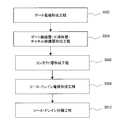
- FIG. 6 is a diagram for explaining the outline of the manufacturing method of the semiconductor device 100.
- the manufacturing method of the semiconductor device 100 includes a gate electrode forming step S602 for forming a gate electrode, and a gate insulating layer, a semiconductor layer, and a channel protective layer for forming a gate insulating layer, a semiconductor layer, and a channel protective layer. It includes a forming step S604, a contact layer forming step S606, a source / drain electrode forming step S608 for forming source and drain electrodes, and a source / drain separation step S610 for electrically separating the source and drain electrodes.
- FIGS. 7 to 12 a method of manufacturing the semiconductor device 100 will be described in detail for each process.
- (a) shows a top view of the first region
- (b) and (c) show cross-sectional views of (a).
- (d) shows a top view of the second region
- (e) and (f) show cross-sectional views of (d).
- Gate electrode formation step S602 As shown in FIGS. 7A to 7F, a gate metal film (not shown) is formed on the substrate 102 and patterned to form gate electrodes 122 and 142. Specifically, first, a gate metal film (not shown) is formed by depositing molybdenum (Mo) with a thickness of 200 nm on a substrate 102 such as a glass substrate by sputtering using argon (Ar) gas. To do. The temperature of the substrate 102 when forming the gate metal film is, for example, 200 to 300 ° C.
- Mo molybdenum
- Ar argon
- a photoresist pattern film (not shown) is formed on the gate metal film, and the gate metal film is patterned using the photoresist pattern film as a mask (photolithography process). Thereby, the gate electrodes 122 and 142 are formed.
- a wet etching method is used for etching the gate metal film.
- the etchant a solution comprising 10 to 90% by weight phosphoric acid, 1 to 10% by weight nitric acid, 1 to 10% by weight acetic acid, and the balance water is used.
- the photoresist pattern film is removed using a stripping solution containing organic alkali.
- the material of the gate electrodes 122 and 142 is indium tin oxide (ITO), tungsten (W), copper (Cu), chromium (Cr), tantalum (Ta), aluminum (Al)
- ITO indium tin oxide
- tungsten W
- Cu copper
- Cr chromium
- Ta tantalum
- Al aluminum
- simple metals such as titanium (Ti), or those containing nitrogen, oxygen, or other metals may be used.
- the gate metal film may be a single layer using the above materials or a laminated structure.
- the gate electrodes 122 and 142 may have a Ti / Al / Ti laminated structure of titanium and aluminum, a Ti / Cu / Ti laminated structure of titanium and copper, or a Mo / Cu / Mo laminated structure of copper and molybdenum. There may be.
- the gate metal film As a method for forming the gate metal film, an evaporation method or the like can be used in addition to the sputtering method. Further, the thickness of the gate metal film is not particularly limited. Also, the etching method of the gate metal film can be appropriately changed according to the material of the gate metal film, and is not limited to the wet etching method described above, but is not limited to chlorine (Cl 2 ) gas, boron trichloride (BCl 3 ). A dry etching method combining gas, CF 4 (carbon tetrafluoride) gas, O 2 (oxygen), or the like can also be used.
- gate insulating layer / semiconductor layer / channel protective layer forming step S604 Gate insulating layer / semiconductor layer / channel protective layer forming step S604 Next, as shown in FIGS. 8A to 8F, gate insulating layers 124 and 144 and microcrystalline silicon films 131 and 151 are sequentially deposited on the gate electrodes 122 and 142, respectively. Thereafter, a silicon nitride film (not shown) is further deposited, and the silicon nitride film is patterned to form channel protective layers 136 and 156.
- the gate insulating layers 124 and 144, the microcrystalline silicon films 131 and 151, and the silicon nitride film are continuously formed in a vacuum using a multi-chamber apparatus.
- the gate insulating layers 124 and 144 can be formed under the same formation conditions as in a general amorphous TFT manufacturing process. Specifically, after the gate electrodes 122 and 142 are formed, gate insulating layers (thickness: 400 nm, for example) 124 and 144 made of silicon nitride (SiN x ) are formed by plasma CVD.
- the gate insulating layers 124 and 144 are formed using a CCP method (capacitive coupling type) plasma CVD under conditions of a substrate temperature of 250 to 300 ° C. and a pressure of 50 to 300 Pa.
- a mixed gas of silane (SiH 4 ), ammonia (NH 3 ), and nitrogen (N 2 ) is used as the source gas.
- the substrate 102 having a stacked structure is transferred to another chamber in a vacuum, and microcrystalline silicon films 131 and 151 having a thickness of 50 nm are formed.
- a CVD method a high density plasma CVD method (ICP method, surface wave plasma method or ECR method) is used, and the substrate temperature is 250 to 300 ° C. and the pressure is about 1.33 Pa.
- Silane (SiH 4 ) and hydrogen (H 2 ) are used as source gases, and the flow ratio of silane and hydrogen is 1:20.
- surface treatment such as hydrogen plasma treatment may be performed on the gate insulating layers 124 and 144 before formation of the microcrystalline silicon film. The pressure at this time is 1.33 Pa, for example.
- the substrate 102 having a laminated structure is transferred to another chamber in a vacuum to form a silicon nitride film having a thickness of 150 nm.
- the silicon nitride film is formed in substantially the same manner as the gate insulating layers 124 and 144.
- a photoresist pattern film (not shown) is formed on the silicon nitride film, and the silicon nitride film is patterned using the photoresist pattern film as a mask (photolithography process). Thereby, island-shaped channel protective layers 136 and 156 are formed.
- a part of the photoresist pattern film can be formed in a self-aligned manner by using a back exposure method together.
- Etching of the silicon nitride film is performed by, for example, a dry etching method mainly using CF 4 (carbon tetrafluoride) gas and O 2 (oxygen) gas, and SF 6 (sulfur hexafluoride) gas and oxygen gas are used. It is also possible. Alternatively, wet etching using hydrofluoric acid is also possible. After completion of the etching, the photoresist pattern film is removed using a stripping solution containing organic alkali.
- contact holes may be formed in the gate insulating layers 124 and 144 as necessary. This contact hole is provided for the purpose of connecting the gate electrodes 122 and 142 to the upper electrode or the like.
- the contact hole can be formed in the same manner as the channel protective layers 136 and 156 described above.
- a photoresist pattern film (not shown) may be formed, and etching may be performed using this photoresist pattern film as a mask.
- an amorphous silicon film (not shown) is formed over the channel protective layers 136 and 156 and the microcrystalline silicon films 131 and 151, and the amorphous silicon film in the second region is formed in the same manner as in the photolithography process described above.
- the thickness is reduced, and amorphous silicon films 133 and 153 are formed as shown in FIGS. 9 (a) to 9 (f).
- an amorphous silicon film with a thickness of 30 nm is formed using CCP (capacitive coupling type) plasma CVD. To do.
- the amorphous silicon film can be formed under the same formation conditions as those for a general amorphous silicon TFT manufacturing process.
- the amorphous silicon film is formed under conditions of a substrate temperature of 250 to 300 ° C. and a pressure of 200 to 500 Pa, and silane (SiH 4 ) gas and hydrogen (H 2 ) gas are used as source gases.
- the flow ratio of silane gas to hydrogen gas is 1:10 to 1: 100.
- surface treatment such as hydrogen plasma treatment may be performed on the microcrystalline silicon films 131 and 151 and the like before formation of the amorphous silicon film.
- the pressure at this time is 1.33 Pa, for example.
- a photoresist pattern film (not shown) is formed on the amorphous silicon film, and the amorphous silicon film is patterned using the photoresist pattern film as a mask (photolithography process). At this time, a photoresist pattern film is arranged as a mask on the amorphous silicon film in the first region so that the amorphous silicon film in the first region is not etched.
- Etching of the amorphous silicon film is performed by, for example, a dry etching method mainly using Cl 2 (chlorine) gas, but other gases can also be used. Etching is performed so that the thickness of the amorphous silicon film in the second region is 10 nm. After completion of the etching, the photoresist pattern film is removed using a stripping solution containing organic alkali.
- n + -type amorphous silicon films 125 and 145 doped with phosphorus are formed on the amorphous silicon films 133 and 153.
- the thicknesses of the n + -type amorphous silicon films 125 and 145 are 30 nm.
- the amorphous silicon films 125 and 145 may be formed in the same manner as the amorphous silicon films 133 and 153 by using a silane gas containing about 0.5% of phosphine (PH 3 ), for example.
- Source / drain electrode formation step S608 Next, as shown in FIGS. 11A to 11F, source / drain metal films (not shown) and photoresist pattern films 137 and 157 are formed on the n + type amorphous silicon films 125 and 145, respectively. Then, the source / drain metal films are patterned using the photoresist pattern films 137 and 157 as masks, thereby forming the source electrodes 127 and 147 and the drain electrodes 128 and 148.
- the source / drain metal film is molybdenum (Mo) having a thickness of 200 nm, and the deposition and patterning of the source / drain metal film are performed in the same manner as the gate electrodes 122 and 142.
- the material of the source / drain metal film may be another material like the gate metal film, or may be a material different from the gate metal film.
- the photoresist pattern films 137 and 157 are left without being removed here, but the photoresist pattern films 137, 157, 157 may be removed.
- Source / drain separation step S610 Next, as shown in FIGS. 12A to 12F, the n + -type amorphous silicon films 125 and 145 and the amorphous silicon films 133 and 153 are etched using the photoresist pattern films 137 and 157 as masks. Further, the microcrystalline silicon films 131 and 151 are etched using the channel protective layers 136 and 156 as masks. The etching at this time is performed by a dry etching method using chlorine (Cl 2 ) gas. The material of the channel protective layers 136 and 156 is silicon nitride, which is hardly etched under an appropriate dry etching condition using chlorine gas and can be used as a mask. Note that the etching method is not limited to the above method, and other gases may be used. The photoresist pattern films 137 and 157 are removed using a stripping solution containing organic alkali after the etching is completed.
- the semiconductor device 100 including the TFT 120 and the TFT 140 is manufactured. Further, a passivation layer (not shown) made of silicon nitride or an organic material may be formed on the TFTs 120 and 140. In addition, a contact hole may be provided in the passivation layer as an opening for obtaining an electrical connection with the source electrodes 127 and 147 from the outside, but the description is omitted here.
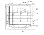
- FIG. 13 is a schematic diagram of an active matrix substrate 200 having the semiconductor device 100.
- a boundary 201 between the display area 202 and the peripheral area 203 of the active matrix substrate 200 is indicated by a double line.
- the display region 202 of the active matrix substrate 200 includes a TFT 120 functioning as a pixel TFT, a gate wiring G electrically connected to the gate electrode of the TFT 120, and a source wiring S electrically connected to the source electrode of the TFT 120.
- a pixel electrode 204 electrically connected to the drain electrode of the TFT 120 and an auxiliary capacitance wiring CS for providing an auxiliary capacitance to the pixel electrode 204 are provided.
- As an electrode for providing the auxiliary capacitance a part of the auxiliary capacitance wiring CS is used as an electrode.
- a gate driver circuit 205 that applies a scanning signal to the gate wiring G
- a source driver IC (Integrated Circuit) 206 that applies a source signal to the source wiring S
- the gate driver circuit 205 and the source driver IC 206 are electrically connected to an external circuit (not shown) through the connection terminal portion 207 and the like.
- a TFT 140 with a high on-current is used as the circuit TFT of the gate driver circuit 205 in the peripheral region 203, and a TFT 120 with a low off-current and a high on / off ratio is used as the pixel TFT in the display region 202. It has been. Since the TFT 140 has a high on-current, the channel width of the TFT can be reduced, whereby the area occupied by the gate driver circuit 205 on the active matrix substrate 200 can be reduced, so that the frame width of the active matrix substrate 200 and the semiconductor device 100 can be reduced. Can be realized.
- the off current of the TFT 120 is low and the on / off ratio is high, the pixel electrode potential is sufficiently maintained even when used as a pixel TFT. For this reason, in the display device, a decrease in contrast ratio can be suppressed, and display quality can be maintained.
- the TFTs 120 and 140 on the active matrix substrate 200 it is possible to realize a narrow frame without deteriorating the display quality.
- source driver IC 206 is provided here, a source driver circuit having the TFT 140 may be provided instead of the source driver IC 206.
- the TFT 140 is used in the gate driver circuit or the source driver circuit.
- the active matrix substrate is provided with a source division driving circuit as disclosed in, for example, Japanese Patent Laid-Open No. 2005-115342, and the source division circuit is provided.
- the TFT 140 may be used for the drive circuit.
- FIG. 14 is a schematic diagram of a source division drive circuit.
- Source lines SRn, SGn, SBn, SRn + 1, SGn + 1, and SBn + 1 are provided on the display area side, and driver lines SRINm, SGINm, and SBINm are provided on the source driver IC side.
- On / off of the TFT 140 is controlled by the switching signal SEL1 or SEL2.
- SEL1 or SEL2 For example, a signal supplied from the source driver IC and supplied via the driver wiring SRINm is divided into source wirings SRn and SRn + 1.
- the on-current of the TFT 140 is high, the circuit area can be reduced and a narrow frame can be realized.
- the TFT 140 with a high on-current is used as the TFT of the gate driver circuit or the source driver circuit.
- the TFT 120 with a low off-current is used as the TFT of the gate driver circuit or the source driver circuit as needed. May be used.
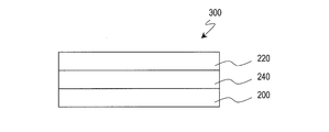
- FIG. 15 shows a schematic diagram of a liquid crystal display device 300 including an active matrix substrate 200.
- the liquid crystal display device 300 includes an active matrix substrate 200, a counter substrate 220, and a liquid crystal layer 240 provided between the active matrix substrate 200 and the counter substrate 220.
- the semiconductor layer 150 has a stacked structure including the microcrystalline silicon film 152 and the amorphous silicon film 154, but the present invention is not limited to this.
- the semiconductor devices 100A, 100B, and 100C will be described with reference to FIGS.
- (a) shows a top view of the first region
- (b) and (c) show cross-sectional views of (a).
- (d) shows a top view of the second region
- (e) and (f) show cross-sectional views of (d).
- the semiconductor layer 150 does not include the amorphous silicon film 154, and the semiconductor layer 150 is formed only from the microcrystalline silicon film 152.
- the TFT 120A is in the first region, and the TFT 140A is in the second region.
- the amorphous silicon film 134 is located between the channel protective layer 136 and the microcrystalline silicon film 132, and similarly, the amorphous silicon film 134 is amorphous silicon.
- the film 154 is located between the channel protective layer 156 and the microcrystalline silicon film 152.
- the TFT 120B is in the first region
- the TFT 140B is in the second region.
- the amorphous silicon film 134 is located between the channel protective layer 136 and the microcrystalline silicon film 132, and the semiconductor layer 150 is amorphous. Without including the silicon film 154, the semiconductor layer 150 is formed only from the microcrystalline silicon film 152.
- the TFT 120C is in the first region
- the TFT 140C is in the second region.
- the semiconductor devices 100A, 100B, and 100C shown in FIGS. 16 to 18 are manufactured in the same manner as the semiconductor device 100.
- the structure of the semiconductor layers 130 and 150 can be changed by changing the film formation order or omitting the film formation.
- a photolithography process may be performed as in the semiconductor device 100.
- a resist pattern film may be formed and etched appropriately.
- the contact layers 126a, 146a, 126b, and 146b are provided between the semiconductor layer 130 and the semiconductor layer 150 and the source electrodes 127 and 147 and the drain electrodes 128 and 148. Is not limited to this.
- the contact layers 126a, 146a, 126b, and 146b may not be provided.
- one of the contact layers 126a and 126b of the TFT 120 and the contact layers 146a and 146b of the TFT 140 may not be provided.
- the manufacturing method in these cases is the same as that of the semiconductor devices 100, 100A, 100B, and 100C.
- the microcrystalline silicon film 152 of the semiconductor layer 150 is formed in the same step as the microcrystalline silicon film 132 of the semiconductor layer 130, and the thickness of the microcrystalline silicon film 152 is the same as that of the microcrystalline silicon film 132. Although it was substantially equal, this invention is not limited to this. The thickness of the microcrystalline silicon film 152 may be different from that of the microcrystalline silicon film 132.
- the microcrystalline silicon film 152 of the semiconductor layer 150 is formed in the same step as the microcrystalline silicon film 132 of the semiconductor layer 130, and the crystallization rate of the microcrystalline silicon film 152 is the microcrystalline silicon film 132.
- the present invention is not limited to this.
- the crystallization rate of the microcrystalline silicon film 152 may be higher than that of the microcrystalline silicon film 132.
- the TFTs of the semiconductor devices 100, 100A, 100B, and 100C have a single gate structure, but the present invention is not limited to this.
- the TFT may have a double gate structure.
- both structures may be mixed so that some TFTs have a double gate structure and other TFTs have a single gate structure.
- FIG. 19 shows a TFT 120D having a double gate structure.
- the TFT 120D may be included in the semiconductor devices 100, 100A, 100B, and 100C.
- FIGS. 19A and 19C show cross-sectional views of the TFT 120D
- FIGS. 19B and 19C correspond to cross sections taken along lines 19b-19b 'and 19c-19c' of FIG. 19A, respectively.
- the TFT 120D includes gate electrodes 122 and 138 provided on the substrate 102, a gate insulating layer 124 covering the gate electrodes 122 and 138, a source electrode 127, a drain electrode 128, an intermediate electrode 129, and a gate insulating layer 124. And the channel protective layers 136 and 139 covering part of the semiconductor layer 130.
- the semiconductor layer 130 includes a microcrystalline silicon film 132 and an amorphous silicon film 134. Note that in the case where the TFT 120D is used, it is desirable to use the TFT 120D as a part of the TFTs in the semiconductor devices 100, 100A, 100B, and 100C.
- the TFT 120D having a double gate structure can be expected to improve the on / off ratio, like the TFT 120 included in the semiconductor devices 100, 100A, 100B, and 100C of this embodiment. There is a demerit that the occupied area becomes large. Therefore, when the TFT 120D is used as a pixel TFT in the first region, the aperture ratio may be lowered. As described above, in the case of improving the on / off ratio, the semiconductor devices 100, 100A, 100B, and 100C described above, and the semiconductor devices 500, 500A, 500B, 500C, 800, and 800A described later are included. As a result, the characteristics of the semiconductor device and the active matrix substrate can be improved more effectively than using a TFT having a double gate structure.
- the channel protective layers 136 and 156 are provided, and the channel protective layers 136 and 156 function as masks for the microcrystalline silicon films 132 and 152; however, the present invention is not limited to this.
- the semiconductor device 500 of this embodiment has a TFT 520 and a TFT 540.
- the TFT 520 and the TFT 540 are inverted staggered channel etching type TFTs.
- FIG. 20A shows a top view of the TFT 520
- FIGS. 20B and 20C show cross-sectional views of the TFT 520
- FIG. FIGS. 20B and 20C correspond to cross sections taken along lines 20b-20b 'and 20c-20c' of FIG. 20A, respectively.
- 20D is a top view of the TFT 540
- FIGS. 20E and 20F are cross-sectional views of the TFT 540.
- FIG. FIGS. 20E and 20F correspond to cross sections taken along lines 20e-20e 'and 20f-20f' of FIG. 20D, respectively.
- the TFT 520 includes a gate electrode 122 provided over the substrate 102, a gate insulating layer 124 covering the gate electrode 122, a source electrode 127, a drain electrode 128, and a semiconductor layer 530 provided over the gate insulating layer 124.
- the semiconductor layer 530 includes a source region 530a, a drain region 530b, and a channel region 530c.
- the source region 530a of the semiconductor layer 530 is electrically connected to the source electrode 127 through the contact layer 126a
- the drain region 530b of the semiconductor layer 530 is electrically connected to the drain electrode 128 through the contact layer 126b. Yes.
- the TFT 540 includes a gate electrode 142 provided over the substrate 102, a gate insulating layer 144 covering the gate electrode 142, a source electrode 147, a drain electrode 148, and a semiconductor layer 550 provided over the gate insulating layer 144. And have.
- the semiconductor layer 550 includes a source region 550a, a drain region 550b, and a channel region 550c.
- the source region 550a of the semiconductor layer 550 is electrically connected to the source electrode 147 through the contact layer 146a
- the drain region 550b of the semiconductor layer 550 is electrically connected to the drain electrode 148 through the contact layer 146b. Yes.
- the thicknesses of the gate insulating layers 124 and 144 are both approximately 400 nm regardless of whether or not they are on the gate electrodes 122 and 142, and the gate insulating layers 124 and 144 are made of silicon nitride (SiN x ).
- the channel lengths L3 and L4 of the TFTs 520 and 540 are the distance between the source electrode 127 and the drain electrode 128, the source electrode 147 and the drain electrode 148, respectively.
- the width of the source electrode 127 is approximately equal to the width of the drain electrode 128, and the width of the source electrode 147 is approximately equal to the width of the drain electrode 148.
- the gate electrode 122 and the gate electrode 142 are formed in the same process, and the gate electrode 122 and the gate electrode 142 are formed of the same material (for example, molybdenum (Mo)).
- the semiconductor layer 530 and the semiconductor layer 550 have a multilayer structure.
- the semiconductor layer 530 includes a microcrystalline silicon film 532 provided over the gate insulating layer 124 and an amorphous silicon film 534 provided over the microcrystalline silicon film 532.
- the semiconductor layer 550 includes a microcrystalline silicon film 552 provided over the gate insulating layer 144 and an amorphous silicon film 554 provided over the microcrystalline silicon film 552.
- the microcrystalline silicon films 532 and 552 are formed of the same material (for example, microcrystalline silicon), and the amorphous silicon films 534 and 554 are formed of the same material (for example, amorphous silicon).
- each of the semiconductor layers 530 and 550 a part of the channel region is removed. Specifically, in the channel region 550c of the semiconductor layer 550, the amorphous silicon film 554 is completely removed and part of the microcrystalline silicon film 552 is removed. On the other hand, part of the amorphous silicon film 534 is removed in the channel region 530c of the semiconductor layer 530, but the microcrystalline silicon film 532 is not removed.
- the contact layers 126a and 126b are provided on the microcrystalline silicon film 532 with the amorphous silicon film 534 interposed therebetween. Similarly, the contact layers 146a and 146b are provided over the microcrystalline silicon film 552 with the amorphous silicon film 554 interposed therebetween.
- passivation layers 536 and 556 are provided so as to cover the channel regions 530c and 550c of the semiconductor layers 530 and 550, the source electrodes 127 and 147, and the drain electrodes 128 and 148, respectively.
- the semiconductor layers 530 and 550 on the gate electrodes 122 and 142 determine basic characteristics of the TFTs 520 and 540.
- the semiconductor layer 550 of the TFT 540 is different from the semiconductor layer 530 of the TFT 520. Specifically, the amorphous silicon film 554 in the source region 550a and the drain region 550b is thinner than the amorphous silicon film 534 in the source region 530a and the drain region 530b. Further, the amorphous silicon film 554 in the channel region 550c is removed, but the amorphous silicon film 534 in the channel region 530c is left. The microcrystalline silicon film 552 in the channel region 550c is thinner than the microcrystalline silicon film 532 in the channel region 530c.
- the thickness of the amorphous silicon film 554 in the source region 550a and the drain region 550b is 10 nm
- the thickness of the amorphous silicon film 534 in the source region 530a and the drain region 530b is 50 nm.
- the thickness of the amorphous silicon film 534 in the channel region 530c is 20 nm.
- the thickness of the microcrystalline silicon film 552 in the channel region 550c is 30 nm
- the thickness of the microcrystalline silicon film 532 in the channel region 530c is 50 nm. Note that the thickness of the microcrystalline silicon films 532 and 552 in the source regions 530a and 550a and the drain regions 530b and 550b is 50 nm.
- the thickness of each of the microcrystalline silicon films 532 and 552 in the channel regions 530c and 550c is preferably 20 nm to 60 nm.
- the thickness of the microcrystalline silicon films 532 and 552 in the channel regions 530c and 550c is less than 20 nm, the mobility and on-current of the TFTs 520 and 540 are reduced.
- the thickness of the microcrystalline silicon films 532 and 552 in the channel regions 530c and 550c exceeds 60 nm, the off currents of the respective TFTs 520 and 540 increase, and the on / off ratio decreases.
- the semiconductor layer 550 includes the microcrystalline silicon film 552, and the on-current of the TFT 540 is large. Further, since the amorphous silicon film 534 of the semiconductor layer 530 in the source region 530a and the drain region 530b is thicker than the amorphous silicon film 554 of the semiconductor layer 550 in the source region 550a and the drain region 550b, the off current of the TFT 520 is small.
- both the on range of the gate voltage Vgd> 0 and the off range of the gate voltage Vgd ⁇ 0 are used.
- the / off ratio is particularly important. Therefore, when the semiconductor layer of the pixel TFT has a microcrystalline silicon film and an amorphous silicon film, the amorphous silicon film has a thickness of 30 nm or more, or the semiconductor layer does not have a microcrystalline silicon film. It is preferable to have.
- the circuit TFT can be designed in the range of the gate voltage Vgd only in the range of Vgd ⁇ 0.
- Circuit TFTs require small TFTs and large currents to narrow the frame or maximize the aperture ratio, especially when they are formed in the peripheral area of a panel or the like, or when a readout circuit is formed in the display area. Therefore, on-current is regarded as important among TFT characteristics. Therefore, the semiconductor layer of the circuit TFT includes a microcrystalline silicon film and, if necessary, an amorphous silicon film, and the thickness of the amorphous silicon film is preferably 0 nm or more and 30 nm or less. Therefore, in the semiconductor device 500, the TFT 520 is preferably used as a pixel TFT, and the TFT 540 is preferably used as a circuit TFT.
- the characteristics of the TFT 520 are different from the characteristics of the TFT 540. Specifically, when the gate voltages are equal, the on-current of the TFT 540 is larger than the on-current of the TFT 520. When the gate voltages are equal, the off-current of the TFT 520 is smaller than the off-current of the TFT 540. Focusing on the ratio of on-current to off-current (on / off ratio), the on / off ratio of the TFT 520 is larger than that of the TFT 540.
- the TFT 520 may be referred to as a first thin film transistor
- the TFT 540 may be referred to as a second thin film transistor.
- a region where the TFT 520 is provided may be referred to as a first region
- a region where the TFT 540 is provided may be referred to as a second region.
- Such a semiconductor device 500 is suitably used for manufacturing an active matrix substrate of a display device.
- the TFT 540 having a high on-current is preferably used as a circuit TFT in the peripheral region, and the TFT 520 having a low off-current is preferably used as a pixel TFT in the display region.
- the semiconductor device 600 includes a TFT 620 provided in the first region and a TFT 640 provided in the second region.
- the TFT 620 has a configuration similar to that of the TFT 640.
- FIGS. 21A is a top view of the TFT 620
- FIGS. 21B and 21C are cross-sectional views of the TFT 620
- FIG. FIGS. 21B and 21C correspond to cross sections taken along lines 21b-21b ′ and 21c-21c ′ of FIG. 21A, respectively.
- FIG. 21D is a top view of the TFT 640
- FIGS. 21E and 21F are cross-sectional views of the TFT 640.
- FIGS. 21E and 21F correspond to cross sections taken along the lines 21e-21e 'and 21f-21f' of FIG. 21D, respectively.
- the TFT 620 includes only the microcrystalline silicon film 632 as the semiconductor layer 630.
- the microcrystalline silicon film 632 is in contact with the gate insulating layer 624 and directly in contact with the contact layers 626a and 626b.
- the TFT 640 includes only the microcrystalline silicon film 652 as the semiconductor layer 650.
- the microcrystalline silicon film 652 is in contact with the gate insulating layer 644 and directly in contact with the contact layers 626a and 626b.
- the thickness of the microcrystalline silicon films 632 and 652 is 30 nm in the channel regions 630c and 650c, and 50 nm in the source regions 630a and 650a and the drain regions 630b and 650b.
- the channel length L0 of the TFTs 620 and 640 is the distance between the source electrode 627 and the drain electrode 628 or the source electrode 647 and the drain electrode 648, respectively.
- L0 3.5 ⁇ m.
- the width of the source electrode 627 is equal to the width of the drain electrode 628
- the width of the source electrode 647 is equal to the width of the drain electrode 648.
- FIG. 22 is a diagram for explaining the outline of the manufacturing method of the semiconductor device 500.
- the manufacturing method of the semiconductor device 500 includes a gate electrode forming step S2202 for forming a gate electrode, a gate insulating layer and a semiconductor layer forming step S2204 for forming a semiconductor layer, and a contact layer.
- Contact layer forming step S2206 to be formed source / drain electrode forming step S2208 for forming source and drain electrodes, source / drain separation step S2210 for electrically separating the source and drain electrodes, and passivation layer forming step S2212 Include.
- FIGS. 23 to 27 show a top view of the first region, and (b) and (c) show cross-sectional views of (a). Similarly, in each of FIGS. 23 to 27, (d) shows a top view of the second region, and (e) and (f) show sectional views of (d).
- the same components as those of the semiconductor device 100 described above are denoted by the same reference numerals, and the description thereof is omitted.
- Gate electrode formation step S2202 The gate electrode formation step S2202 is the same as the gate electrode formation step S602 in the semiconductor device 100 described above with reference to FIG. 7, and a detailed description thereof will be omitted.
- the gate electrode 122 and the gate electrode 142 are formed in the same process, and the gate electrode 122 and the gate electrode 142 are formed of the same material (for example, molybdenum (Mo)).
- the materials of the gate electrodes 122 and 142 are in addition to molybdenum (Mo), indium tin oxide (ITO), tungsten (W), copper (Cu), chromium (Cr), and tantalum. It may be a single metal such as (Ta), aluminum (Al), titanium (Ti) or the like, or those containing nitrogen, oxygen, or other metals.
- the gate electrodes 122 and 142 may be a single layer using the above materials or may have a stacked structure.
- the gate electrodes 122 and 142 may have a Ti / Al / Ti laminated structure of titanium and aluminum, a Ti / Cu / Ti laminated structure of titanium and copper, or a Mo / Cu / Mo laminated structure of copper and molybdenum. There may be.
- a method for forming the gate metal film an evaporation method or the like can be used in addition to the sputtering method.
- the thickness of the gate metal film is not particularly limited.
- the method for etching the gate metal film is not limited.
- gate insulating layer / semiconductor layer forming step S2204 As shown in FIGS. 23A to 23F, gate insulating layers 124 and 144, a microcrystalline silicon film (not shown), and an amorphous silicon film are formed on the gate electrodes 122 and 142, respectively. (Not shown) are sequentially deposited, and the microcrystalline silicon film and the amorphous silicon film are patterned in the same photolithography process. Thereafter, the amorphous silicon film in the second region is thinned by another photolithography process to form microcrystalline silicon films 531 and 551 and amorphous silicon films 533 and 553.
- the gate insulating layers 124 and 144, the microcrystalline silicon film, and the amorphous silicon film are continuously formed in a vacuum using a multi-chamber apparatus.
- the gate insulating layers 124 and 144 can be formed under the same formation conditions as in a general amorphous TFT manufacturing process.
- the gate insulating layers for example, 400 nm thick
- the gate insulating layers are formed by plasma CVD. Form.
- the gate insulating layers 124 and 144 are formed using a CCP method (capacitive coupling type) plasma CVD under conditions of a substrate temperature of 250 to 300 ° C. and a pressure of 50 to 300 Pa. Further, a mixed gas of silane (SiH 4 ), ammonia (NH 3 ), and nitrogen (N 2 ) is used as a source gas.
- CCP method capactive coupling type plasma CVD under conditions of a substrate temperature of 250 to 300 ° C. and a pressure of 50 to 300 Pa.
- a mixed gas of silane (SiH 4 ), ammonia (NH 3 ), and nitrogen (N 2 ) is used as a source gas.
- the substrate 102 having a stacked structure is transferred to another chamber in a vacuum, and a microcrystalline silicon film with a thickness of 50 nm is formed.
- CVD is performed using a high-density plasma CVD method (ICP method, surface wave plasma method or ECR method) under conditions of a substrate temperature of 250 to 300 ° C. and a pressure of about 1.33 Pa.
- silane (SiH 4 ) and hydrogen (H 2 ) are used as the source gas, but the flow ratio of silane and hydrogen is 1:20.
- surface treatment such as hydrogen plasma treatment may be performed on the gate insulating layers 124 and 144 before formation of the microcrystalline silicon film. The pressure at this time is 1.33 Pa, for example.
- the substrate 102 having a stacked structure is transferred to another chamber in a vacuum, and an amorphous silicon film having a thickness of 50 nm is formed.
- the amorphous silicon film can be formed under the same formation conditions as those for a general amorphous silicon TFT manufacturing process.
- the amorphous silicon film is formed under conditions of a substrate temperature of 250 to 300 ° C. and a pressure of 200 to 500 Pa, and silane (SiH 4 ) gas and hydrogen (H 2 ) gas are used as source gases.
- the flow ratio of silane gas to hydrogen gas is 1:10 to 1: 100.
- surface treatment such as hydrogen plasma treatment may be performed on the microcrystalline silicon film or the like before formation of the amorphous silicon film.
- the pressure at this time is 1.33 Pa, for example.
- a photoresist pattern film (not shown) is formed on the amorphous silicon film, and the microcrystalline silicon film and the amorphous silicon film are patterned using the photoresist pattern film as a mask (photolithography process). Further, a photoresist pattern film (not shown) is formed on the amorphous silicon film in the first region, and the amorphous silicon film in the second region is thinned using this photoresist pattern film as a mask (photolithography process). As a result, island-shaped amorphous silicon films 533 and 553 and microcrystalline silicon films 531 and 551 are formed.
- Etching of the microcrystalline silicon film and the amorphous silicon film is performed by, for example, a dry etching method mainly using Cl 2 (chlorine) gas, but other gases can also be used.
- Etching in the second photolithography process is performed so that the thickness of the amorphous silicon film is 10 nm in the second region.
- the photoresist pattern film is removed using a stripping solution containing organic alkali.
- contact holes may be formed in the gate insulating layers 124 and 144 as necessary. This contact hole is provided for the purpose of connecting the gate electrodes 122 and 142 to the upper electrode or the like.
- the contact hole may be formed by forming a photoresist pattern film (not shown) and performing etching using this photoresist pattern film as a mask.
- n + -type amorphous silicon films 125 and 145 doped with phosphorus are formed on the amorphous silicon films 533 and 553.
- the thicknesses of the n + -type amorphous silicon films 125 and 145 are 30 nm.
- the amorphous silicon films 125 and 145 are formed using a silane gas containing, for example, about 0.5% of phosphine (PH 3 ) in the same manner as the amorphous silicon film in the gate insulating layer / semiconductor layer forming step S2204, which is the previous step. Also good.
- Source / drain electrode formation step S2208 Next, as shown in FIGS. 25A to 25F, source / drain metal films (not shown) and photoresist pattern films 137 and 157 are formed on the n + -type amorphous silicon films 125 and 145, respectively. Then, by patterning the source / drain metal film, the source electrodes 127 and 147 and the drain electrodes 128 and 148 are formed.
- the source / drain metal film is molybdenum (Mo) with a thickness of 200 nm, and the deposition and patterning of the source / drain metal film are performed in the same manner as the gate electrodes 122 and 142.
- the material of the source / drain metal film may be another material like the gate metal film, or may be a material different from the gate metal film.
- the photoresist pattern films 137 and 157 are left without being removed here, but the photoresist pattern films 137, 157, 157 may be removed.
- Source / drain separation step S2210 the n + -type amorphous silicon films 125 and 145, the amorphous silicon films 533 and 553, and a part of the microcrystalline silicon film 551 are etched using the photoresist pattern films 137 and 157 as a mask.
- the etching at this time is performed by a dry etching method using chlorine (Cl 2 ) gas. Note that the etching method is not limited to the above method, and other gases may be used.
- the photoresist pattern films 137 and 157 are removed.
- the photoresist pattern films 137 and 157 are removed using a stripping solution containing organic alkali after the etching is completed.
- passivation layer forming step S2212 Next, as shown in FIGS. 27A to 27F, passivation layers 536 and 556 are formed.
- the passivation layers 536 and 556 can be formed under the same formation conditions as in a general amorphous TFT manufacturing process. Specifically, after the source / drain separation step S2210, the passivation layers 536 and 556 (thickness :, for example, 250 nm) made of silicon nitride (SiN x ) are formed by plasma CVD as in the formation of the gate insulating layers 124 and 144. ).
- the passivation layers 536 and 556 are formed under the conditions of substrate temperature: 250 to 300 ° C.
- a mixed gas of silane (SiH 4 ), ammonia (NH 3 ), and nitrogen (N 2 ) is used as the source gas.
- silane SiH 4
- NH 3 ammonia
- N 2 nitrogen
- an organic material specifically, a photosensitive organic material can be used, or silicon nitride and silicon oxide (SiO x ) may be used in combination.
- the semiconductor device 500 including the TFT 520 and the TFT 540 is manufactured.
- a photolithography step may be further performed to form contact holes in the passivation layers 536 and 556 as openings for obtaining electrical connection with the source electrodes 127 and 147 from the outside. .
- the amorphous silicon films 533 and 553 having different thicknesses are formed by performing two photolithography steps, but the present invention is not limited thereto.
- amorphous silicon films 533 and 553 having different thicknesses can be formed by using halftone exposure. In this case, the number of formations of the photoresist pattern film can be reduced, and the material for forming the photoresist pattern film can be reduced.
- the process using halftone exposure is, for example, C.I. W. SID 2000 DIGEST, pp 1006-1009 by Kim et al.
- a thick photoresist pattern film is formed on the amorphous silicon film in the first region using halftone exposure.
- a thin photoresist pattern film is formed on the amorphous silicon film in the second region.
- the amorphous silicon film and the microcrystalline silicon film are etched using all the photoresist pattern film, and then the entire photoresist pattern is thinned by dry etching or the like, thereby removing the thin portion of the photoresist pattern film and leaving the remaining portion.
- the photoresist pattern film in the first region the amorphous silicon film in the second region is thinned.
- the halftone exposure process is applied to the semiconductor device 500, the number of times the photoresist pattern film is formed can be made the same as that of the semiconductor device 600 of Comparative Example 1, so that productivity is improved. Therefore, the combined use of the halftone exposure process is effective for forming the semiconductor device 500.
- contact holes can be formed in the gate insulating layers 124 and 144 and the passivation layers 536 and 556 by halftone exposure using the same photoresist pattern film, and the combination of layers to be processed Are various.
- the process using halftone exposure can also be used in other embodiments.
- the thickness of the microcrystalline silicon films 532 and 552 is preferably 20 nm to 60 nm.
- the thickness of the microcrystalline silicon film is less than 20 nm, the mobility is lowered and the on-characteristic of the TFT is lowered.
- the thickness of the microcrystalline silicon film exceeds 60 nm, the off-current of the TFT increases and the on / off ratio decreases.
- FIG. 28 is a graph showing in detail the relationship between the thickness of the semiconductor layer in the channel region and the TFT characteristics at a source voltage Vsd of 10 V in each of a number of inverted staggered channel etching TFTs.
- the horizontal axis indicates the thickness of the semiconductor layer in the channel region
- the vertical axis indicates the mobility, the minimum off-state current, and the S value.
- the TFT 620 having the shape shown in FIGS.
- the semiconductor layer 630 includes only the microcrystalline silicon film 632, and the source region 630a and the drain region 630b are formed.
- the thickness of the semiconductor layer 630 is 100 nm.
- the channel length of the TFT is 3 ⁇ m and the channel width W is 20 ⁇ m.
- the mobility shows a substantially constant high value.
- the minimum off-current is within the allowable range (15 pA).
- the subthreshold swing value S value falls within the allowable range (2.1 V / decade). .
- the thickness of the semiconductor layer in the channel region is 20 nm or more and 60 nm or less, high mobility (ON characteristics) and low OFF current (minimum OFF current) can be achieved and the subthreshold swing value is set as desired. I understand that I can do it.
- FIG. 28 shows the result of the inverted staggered channel etching type TFT structure, but it is confirmed that the same result can be obtained even with the TFT having the inverted staggered channel protection type TFT structure described in the first embodiment. ing.
- the thickness of the microcrystalline silicon film in the channel region is preferably in the range of 20 nm to 60 nm.
- the semiconductor layer 550 has a stacked structure including the microcrystalline silicon film 552 and the amorphous silicon film 554, but the present invention is not limited thereto.
- the semiconductor device 500A of this embodiment includes a TFT 520A provided in the first region and a TFT 540A provided in the second region.
- FIG. 29A shows a top view of the first region of the semiconductor device 500A
- FIGS. 29B and 29C show cross-sectional views of FIG. 29A
- FIG. 29D is a top view of the second region of the semiconductor device 500A
- FIGS. 29E and 29F are cross-sectional views of FIG. 29D.
- the semiconductor layer 550 does not include the amorphous silicon film 554, and the semiconductor layer 550 is formed only from the microcrystalline semiconductor film 552.
- the semiconductor layer 550 of the semiconductor device 500A can be formed by etching all of the amorphous silicon film in the second region in the second photolithography process in the gate insulating layer / semiconductor layer forming process S2204 described above.
- the amorphous silicon film in the second thin film transistor is thinner than the amorphous silicon film in the first thin film transistor, or the semiconductor layer in the second thin film transistor has no amorphous silicon film, but the present invention is not limited to this. .
- the semiconductor device 500B of this embodiment includes a TFT 520B provided in the first region and a TFT 540B provided in the second region.
- FIG. 30 (a) shows a top view of the first region
- FIGS. 30 (b) and 30 (c) show cross-sectional views of FIG. 30 (a).
- FIG. 30D shows a top view of the second region
- FIGS. 30E and 30F show cross-sectional views of FIG. 30D.
- the TFT 520B includes a gate electrode 122, a gate insulating layer 524B, a source electrode 127, a drain electrode 128, and a semiconductor layer 530.
- the semiconductor layer 530 includes a source region 530a, a drain region 530b, and a channel region 530c.
- the source region 530a of the semiconductor layer 530 is electrically connected to the source electrode 127 via the contact layer 126a
- the drain region 530b of the semiconductor layer 130 is electrically connected to the drain electrode 128 via the contact layer 126b. Yes.
- the TFT 540B includes a gate electrode 142, a gate insulating layer 544B, a source electrode 147, a drain electrode 148, and a semiconductor layer 550.
- the semiconductor layer 550 includes a source region 550a, a drain region 550b, and a channel region 550c.
- the source region 550a of the semiconductor layer 550 is electrically connected to the source electrode 147 through the contact layer 146a, and the drain region 550b of the semiconductor layer 550 is electrically connected to the drain electrode 148 through the contact layer 146b. Yes.
- the semiconductor layer 530 of the TFT 520B has the same configuration as the semiconductor layer 550 of the TFT 540B, and the semiconductor layer 530 and the semiconductor layer 550 have a single-layer structure.
- the semiconductor layer 530 includes only the microcrystalline silicon film 532 having a thickness of 50 nm.
- the semiconductor layer 550 includes only the microcrystalline silicon film 552 having a thickness of 50 nm.
- the gate insulating layer 524B and the gate insulating layer 544B are made of, for example, silicon nitride (SiN x ), and the thickness of the gate insulating layer 524B is different from that of the gate insulating layer 544B.
- the thickness of the gate insulating layer 524B is 400 nm, and the thickness of the gate insulating layer 544B is approximately 2/3 of the gate insulating layer 524B and is approximately 266 nm.
- the gate insulating layer 544B is thinner than the gate insulating layer 524B.
- the semiconductor device 500B is manufactured in the same manner as the semiconductor device 500.
- the gate insulating layers 524B and 544B of the semiconductor device 500B are partially formed by, for example, depositing a silicon nitride film (SiN x ) to be a gate insulating layer and then performing a photolithography process to partially form the silicon nitride film in the second region. It is formed by etching.
- the method for forming the gate insulating layers 524B and 544B is not limited to this.
- the gate insulating layer 544B of the TFT 540B is thinner than the gate insulating layer 524B. Therefore, even if the gate voltage Vgd is the same, the electric field strength applied to the semiconductor layer 550 is the electric field applied to the semiconductor layer 530. Stronger than strength. Therefore, when the gate voltage Vgd is the same, the on-current of the TFT 540B is larger than that of the TFT 520B.
- Such a TFT 540B has a large off-current when the gate voltage Vgd ⁇ 0, but an increase in off-current does not cause a problem when the TFT 540B is operated in the range of the gate voltage Vgd ⁇ 0.
- the TFT 540B for the TFT driven in the range of Vgd ⁇ 0 among the circuit TFTs.
- the gate insulating layer 524B of the TFT 520B has a thickness of 400 nm similarly to the gate insulating layers 124 and 144 in the semiconductor device 100 described above, and the potential of the pixel electrode is sufficiently maintained even when used as a pixel TFT. Therefore, a reduction in contrast ratio can be suppressed and display quality can be maintained.
- the semiconductor device 500B is appropriately provided with TFTs 520B and 540B having different gate insulating layers 524B and 544B, and the monolithic substrate using the semiconductor device 500B realizes a narrow frame without deteriorating display quality. it can.
- An active matrix substrate of a display device is preferably manufactured using such a semiconductor device 500B.
- the TFT 540B having a high on-current is preferably used as a circuit TFT in the peripheral region, and the TFT 520B having a low off-current is preferably used as a pixel TFT in the display region.
- the semiconductor layer 530 of the TFT 520B has the same structure as the semiconductor layer 550 of the TFT 540B, and the semiconductor layer 530 and the semiconductor layer 550 have a single-layer structure. It is not limited to.
- the semiconductor layer 530 and the semiconductor layer 550 may have a stacked structure of a microcrystalline silicon film and an amorphous silicon film. Note that in the semiconductor device 500B, the semiconductor layer 530 of the TFT 520B may have a different structure from the semiconductor layer 550 of the TFT 540B.
- each of the gate insulating layer 524B and the gate insulating layer 544B has a single layer structure, but the present invention is not limited to this.
- FIG. 31 shows a semiconductor device 500C.
- FIG. 31A shows a top view of the first region of the semiconductor device 500C
- FIGS. 31B and 31C show cross-sectional views of FIG. 31A.
- FIG. 31 (d) shows a top view of the second region
- FIGS. 31 (e) and 31 (f) show cross-sectional views of FIG. 31 (d).
- the same reference numerals are given to the same components as those of the semiconductor device 500 illustrated in FIG. 20, and description thereof is omitted.
- the gate insulating layer 524C has a stacked structure of an insulating layer 524C1 and an insulating layer 524C2, and the gate insulating layer 544C has a single-layer structure.
- the insulating layer 524C1 has a structure similar to that of the gate insulating layer 544C.
- the insulating layer 524C1 and the gate insulating layer 544C are 200 nm thick silicon oxide films (SiO x ), and the insulating layer 524C2 is a 50 nm thick silicon nitride film (SiN x ).
- the semiconductor device 500C is manufactured in the same manner as the semiconductor device 500 described above.
- the silicon oxide film can be formed by a plasma CVD method using TEOS (tetraethoxysilane) as a raw material in the same manner as the silicon nitride film.
- TEOS tetraethoxysilane
- the semiconductor device 500C may be manufactured in a mode different from that of the semiconductor device 500.
- the semiconductor layer 550 has a configuration different from that of the semiconductor layer 530.
- the semiconductor layers 530 and 550 are both formed of a single layer of microcrystalline silicon films 532 and 552, a difference in crystallization rate occurs due to a difference in material of the surface of the base insulating layer.
- the microcrystalline silicon film 532 is formed over the insulating layer 524C2 made of silicon nitride, while the microcrystalline silicon film 552 is a gate insulating layer made of silicon oxide. Since it is formed over 544C, the crystallization rate of the microcrystalline silicon film 552 is higher than that of the microcrystalline silicon film 532.
- the higher the crystallinity of the microcrystalline silicon film the higher the mobility of the TFT.
- the crystallization rate of the microcrystalline silicon film 552 is high, the mobility of the TFT 540C is high and the on-state current is large. Therefore, the TFT 540C is suitable for the circuit TFT, and the area occupied by the driver circuit on the active matrix substrate can be reduced.
- the crystallization rate of the microcrystalline silicon film 532 is relatively low, the characteristics of the TFT 520C are close to those of an amorphous silicon TFT, and have low mobility and low on-current, but have a small off-current and a high on / off ratio.
- the TFT 520C is used as a pixel TFT, the pixel electrode potential is sufficiently maintained, so that a reduction in contrast ratio can be suppressed and display quality can be maintained.
- the semiconductor device 500C is provided with the TFTs 520C and 540C having different gate insulating layers and microcrystalline silicon films having different crystallization ratios on the substrate.
- a narrow frame can be realized without degrading the quality.
- the gate insulating layer 524B and the gate insulating layer 544B are both formed of the same material; however, the present invention is not limited to this.
- the gate insulating layer 524B and the gate insulating layer 544B may be formed of different materials.
- the gate insulating layer 524B may be a single layer of silicon nitride film (SiN x ), and the gate insulating layer 544B may be a single layer of silicon oxide film (SiO x ).
- the thickness of the gate insulating layer 524B is 400 nm, and the thickness of the gate insulating layer 544B is 200 nm.
- the semiconductor layers 530 and 550 are both formed of a single layer of microcrystalline silicon films 532 and 552, even in such a case, a difference in crystallization rate occurs due to a difference in material of the surface of the base insulating layer. To do. In this case, since the crystallinity of the microcrystalline silicon film 552 is higher than that of the microcrystalline silicon film 532, the mobility of the TFT 540B is high and the on-current is large. Therefore, the TFT 540B is suitable as a circuit TFT, and the area occupied by the driver circuit on the active matrix substrate can be reduced.
- the crystallization rate of the microcrystalline silicon film 532 is relatively low, the characteristics of the TFT 520B are close to those of an amorphous silicon TFT, and the mobility is low and the on-current is small, but the off-current is small and the on / off ratio is high.
- the TFT 520B is used as a pixel TFT, the pixel electrode potential is sufficiently maintained, so that a reduction in contrast ratio can be suppressed and display quality can be maintained.
- the TFT 520B is suitable as a pixel TFT because the microcrystalline silicon film 532 is formed on the surface of the gate insulating layer 524B made of a silicon nitride film (SiN x ).
- the microcrystalline silicon film 552 is a silicon oxide film. Since it is formed on the surface of the gate insulating layer 544B made of (SiO x ), it has characteristics suitable as a circuit TFT.
- TFTs 520B and 540B having different gate insulating layers and microcrystalline silicon films having different crystallization ratios are appropriately provided over a substrate. Therefore, in a semiconductor device having a gate driver circuit or the like Therefore, it is possible to realize a narrow frame without degrading display quality.
- the semiconductor device includes TFTs having different characteristics, but the present invention is not limited to this.
- the semiconductor device may include a semiconductor element other than the TFT.
- the semiconductor device 800 of this embodiment includes a TFT 820 and a diode 860.
- a diode 860 is a photodiode in which TFTs are diode-connected.
- FIG. 32 shows a schematic cross-sectional view of the TFT 820 and the diode 860.
- the TFT 820 includes a gate electrode 122 provided over the substrate 102, a gate insulating layer 124 covering the gate electrode 122, a source electrode 127, a drain electrode 128, and a semiconductor layer 530 provided over the gate insulating layer 124.
- the semiconductor layer 530 includes a microcrystalline silicon film 532 and an amorphous silicon film 534.
- the source region 530a of the semiconductor layer 530 is electrically connected to the source electrode 127 through the contact layer 126a, and the drain region 530b of the semiconductor layer 530 is electrically connected to the drain electrode 128 through the contact layer 126b. Yes.
- the diode 860 includes a gate electrode 162 provided over the substrate 102, a gate insulating layer 164 covering the gate electrode 162, a first electrode (source electrode) 167, a second electrode (drain electrode) 168, a gate, A semiconductor layer 170 provided over the insulating layer 164;
- the semiconductor layer 170 includes a microcrystalline silicon film 172 and an amorphous silicon film 174.
- the source region 170a of the semiconductor layer 170 is electrically connected to the first electrode 167 via the contact layer 166a, and the drain region 170b of the semiconductor layer 170 is electrically connected to the second electrode 168 via the contact layer 166b.
- the channel length of the TFT 820 corresponds to the distance between the source electrode 127 and the drain electrode 128, and is, for example, 3.5 ⁇ m.
- the channel length of the diode 860 corresponds to the distance between the first electrode 167 and the second electrode 168 and is, for example, 10 ⁇ m.
- at least one of the first electrode (source electrode) 167 and the second electrode (drain electrode) 168 of the diode 860 may have a U-shaped planar shape at a part thereof.
- the total extension of the gap (gap) formed by one electrode (source electrode) 167 and the second electrode (drain electrode) 168 corresponds to the channel width.
- the source electrode or the drain electrode may have a U-shaped planar shape.
- the channel width of the TFT 820 corresponds to the electrode width of the source electrode 127 and is 24 ⁇ m.
- the channel width of the diode 860 corresponds to the width of the first electrode 167 and the second electrode 168 and is 150 ⁇ m.
- the source electrode 127 and the source electrode 128 have the same width
- the first electrode 167 and the second electrode 168 have the same width.
- each of the semiconductor layers 530 and 170 part of the channel regions 530c and 170c are removed.
- the thickness of the microcrystalline silicon films 532 and 172 is 50 nm, and the thickness of the amorphous silicon films 534 and 174 is 80 nm. However, the thickness of the amorphous silicon film in the channel regions 530c and 170c is 50 nm.
- the gate electrode 162 is electrically connected to the first electrode 167 through a contact hole 179 provided in the gate insulating layer 164.
- a diode 860 can be used as a photodiode.
- the diode 860 has a very small dark current.
- a photocurrent is generated, and the potential of a separately provided storage capacitor portion changes. This change in potential is read out to the outside by a predetermined wiring and a reading circuit or the like, and signal processing is performed to obtain intensity information of light received by the diode 860.
- the semiconductor layer 170 of the diode 860 includes the amorphous silicon film 174 as well as the microcrystalline silicon film 172. As described above, since the semiconductor layer 170 includes the amorphous silicon film 174, the diode current with respect to the external light intensity can be increased, so that the sensitivity as a photodiode is improved.
- the semiconductor device of Comparative Example 2 has a photodiode having only a microcrystalline silicon film as a semiconductor layer.
- FIG. 33 shows the characteristics of the photodiode in the semiconductor device of Comparative Example 2 and the characteristics of the photodiode 860 in the semiconductor device 800.
- FIG. Here, external light is emitted from the opposite side of the substrate 102 in the normal direction of the main surface of the substrate 102.
- the diode current of the photodiode in the semiconductor device of Comparative Example 2 does not increase so much regardless of the increase in external light intensity.
- the diode current of the diode 860 in the semiconductor device 800 greatly increases as the external light intensity increases, so that the sensitivity and the S / N ratio can be improved. This is because in the semiconductor device 800, the amorphous silicon film 174 receives external light and generates a photocurrent.
- Such an active matrix substrate including the semiconductor device 800 is suitably used for a display device incorporating a photosensor and / or a touch panel function using the photosensor.
- the thickness of each of the microcrystalline silicon films 532 and 172 in the channel regions 530c and 170c is preferably 20 nm to 60 nm.
- the thickness of the microcrystalline silicon film in the channel regions 530c and 170c is less than 20 nm, the mobility is lowered, and the on characteristics and photocurrent of the TFT and the diode are lowered.
- the thickness of the microcrystalline silicon film exceeds 60 nm, the off current and dark current of the TFT and diode increase, and the on / off ratio and S / N ratio decrease.
- the thickness of the amorphous silicon film 174 in the diode 860 is preferably 30 nm or more in the channel region 170c. In this case, since the diode current generated in response to external light is large, it is preferably used as a photosensor.
- FIG. 34A shows a schematic diagram of the active matrix substrate 1000.
- FIG. 34B shows a schematic circuit diagram of a liquid crystal display device 1100 including the active matrix substrate 1000
- FIG. 34C shows a schematic diagram of the liquid crystal display device 1100.
- FIG. 34 (d) shows a schematic circuit diagram of another liquid crystal display device 1100A including the active matrix substrate 1000.
- the active matrix substrate 1000 includes a source line S, a read line R, an auxiliary capacitance line CS, a gate line G, a pixel region 1106, and a sensor region 1107. Yes.
- the storage capacitor line CS extends in parallel with the gate line G.
- the readout wiring R extends in parallel with the source wiring S.
- the pixel region 1106 is provided with a pixel electrode 135, a TFT 820 having a semiconductor layer 530, a connection wiring 1111, and a contact hole 180.
- the pixel electrode 135 is drained through the connection wiring 1111 and the contact hole 180.
- the electrode 128 is electrically connected.
- a capacitive coupling is formed between the connection wiring 1111 and the auxiliary capacitance wiring CS, which contributes to holding the pixel potential.
- a source electrode 127 of the TFT 820 is connected to the source wiring S.
- a diode 860 having a semiconductor layer 170, a TFT 880 having a semiconductor layer 590, a contact hole 181 and a connection wiring 1110 are provided in the sensor region 1107.
- capacitive coupling is formed between the auxiliary capacitance wiring CS and a branch portion thereof to form a storage capacitor portion 1112.
- the connection wiring 1110 connects the drain electrode 188 of the TFT 880 and the second electrode (drain electrode) 168 of the diode 860.
- a source electrode 187 of the TFT 880 is connected to the readout wiring R.
- the first electrode (source electrode) 167 of the diode 860 is connected to the auxiliary capacitance line CS through the contact hole 181.
- the TFT 880 and the semiconductor layer 590 have the same structure as the TFT 820 and the semiconductor layer 530, respectively, but the planar shape and size are not necessarily the same.
- COM is a common electrode (not shown) on the counter substrate
- Clc is a capacitance between the common electrode on the counter substrate and the pixel electrode 135
- Ccs is between the connection wiring 1111 and the auxiliary capacitance wiring CS.
- Cps represents the capacitance between the connection wiring 1110 and the auxiliary capacitance wiring CS.
- the liquid crystal display device 1100 includes an active matrix substrate 1000, a counter substrate 1101, a light shielding layer 1102, an opening 1103 provided in the light shielding layer 1102, TFTs 820 and 880, a diode. 860, a pixel electrode 135, a color filter 1105, and a liquid crystal layer 1104 provided between the active matrix substrate 1000 and the counter substrate 1101.
- the active matrix substrate 1000 and the liquid crystal display device 1100 described above are merely examples, and the present invention is not limited thereto.
- the region 1108 includes both the pixel region 1106 and the sensor region 1107, and one photosensor may be provided for each pixel.
- the circuit diagrams shown in FIGS. 34 (b) and 34 (d) may have other forms.
- the semiconductor layers 130 and 150 and / or the gate insulating layers 124 and 144 of the TFTs 120 and 140 are different from each other, and the semiconductor devices 100A, 100B, 100C, 500, 500A, 500B, and 500C are similarly semiconductors.
- the layers and / or gate insulating layers are different from each other.
- the semiconductor layers 530 and 170 and the gate insulating layers 124 and 164 of the TFT 820 and the diode 860 may have the same configuration or may be different.
- the semiconductor device 800 may further include the TFT 540 of the semiconductor device 500 described above in addition to the TFT 820 and the diode 860.
- the TFTs 820 and 540 are also called a first thin film transistor and a second thin film transistor, respectively.
- the thickness of the amorphous silicon film 554 of the semiconductor layer 550 of the TFT 540 is, for example, 10 ⁇ m, and the amorphous silicon film 174 in the diode 860 is thinner than the amorphous silicon film 554.
- the TFT 820 is suitable as a pixel TFT because the off-state current is low and the on / off ratio is high
- the TFT 540 is suitable as a circuit TFT because the on-state current is large.
- the diode 860 is suitable as a sensor that senses a change in external light intensity as a photodiode.
- the TFT 540, the TFT 820, and the diode 860 having different semiconductor layers are appropriately arranged on the substrate in the semiconductor device 800. Therefore, in the semiconductor device having a gate driver circuit and the like, the frame is narrowed without deteriorating the display quality.
- a photodiode can be formed to incorporate a touch panel function.
- the semiconductor layer 530 of the TFT 820 includes the microcrystalline silicon film 532 and the amorphous silicon film 534, but the present invention is not limited to this.
- the semiconductor layer 530 of the TFT 820A does not have a microcrystalline silicon film, but is formed only from an amorphous silicon film 534.
- the semiconductor device 800A similarly includes the diode 860 included in the semiconductor device 800, but the semiconductor device 800A may further include a TFT 540.
- the TFTs of the semiconductor devices 100, 100A, 100B, 100C, 500, 500A, 500B, 500C, 800, and 800A have a single gate structure, but the present invention is not limited to this.
- the TFT may have a double gate structure, or both a double gate structure and a single gate structure may be mixed.
- the semiconductor device may be used for an organic EL (Organic Light Emitting Diode: OLED) display device.
- the organic EL display device is a current driving type, and one pixel is composed of two or more TFTs, a driving TFT for driving the organic EL element and a switching TFT for switching the driving TFT.
- FIG. 36 shows an example of a pixel equivalent circuit of an organic EL display device 1300 having the semiconductor device 1200 of this embodiment.
- the organic EL display device 1300 includes a source line 1301, a gate line 1302, a supply line 1303, an organic EL element 1306, a cathode 1304 and an anode 1305 for applying a predetermined voltage to the organic EL element 1306, and a display signal.
- the drive TFT 1309 always keeps flowing a current, and thus a high on-current is required.
- the TFTs 1308 and 1309 of the semiconductor device 1200 have the same configuration as the TFTs 520 and 540 of the semiconductor device 500 described above.
- the switching TFT 1308 has the same configuration as the TFT 520
- the driving TFT 1309 has the same configuration as the TFT 540. Therefore, each semiconductor layer of the switching TFT 1308 and the driving TFT 1309 has a microcrystalline silicon film and an amorphous silicon film, and the amorphous silicon film in the source region and the drain region of the semiconductor layer in the switching TFT 1308 is thick, and the semiconductor layer in the driving TFT 1309 The amorphous silicon film in the source and drain regions is thin.
- the switching TFT 1308 has a high on / off ratio, it is possible to appropriately hold an analog voltage as a display signal and realize a good display.
- the driving TFT 1309 has a microcrystalline silicon film and has a large on-current, the size of the TFT can be reduced with the same on-current. For this reason, a display with high luminance can be realized by advantages such as an increase in the aperture ratio and an increase in the area of the organic EL element.
- the semiconductor device 1200 is suitably used as an organic EL display device, and can realize high luminance.
- the semiconductor device 1200 may have a structure similar to any of the structures of the semiconductor devices 100, 100A, 100B, 100C, 500, 500A, 500B, 500C, 800, and 800A described above, and includes a microcrystalline silicon film and an amorphous structure.
- the thickness of the silicon film may have the same structure as any of the semiconductor devices 100, 100A, 100B, 100C, 500, 500A, 500B, 500C, 800, and 800A described above. The same applies to the optimum range.
- a microcrystalline silicon film is described as an example of a microcrystalline semiconductor film; however, the present invention is not limited to this.
- the microcrystalline semiconductor film may contain silicon and germanium.
- the microcrystalline semiconductor film may contain silicon and gallium, or may contain silicon and barium.
- the microcrystalline semiconductor film may contain silicon and a metal element (nickel, molybdenum, neodymium, titanium, vanadium, niobium, or any combination thereof).
- the microcrystalline semiconductor film is formed using a metal oxide semiconductor such as a Zn—O based semiconductor (ZnO) film, an In—Zn—O based semiconductor (IZO) film, or a Zn—Ti—O based semiconductor (ZTO) film. Also good.
- an amorphous silicon film is described as an example of an amorphous semiconductor film, but the present invention is not limited to this.
- the amorphous semiconductor film may contain silicon and germanium.
- the amorphous semiconductor film may contain silicon and gallium, or may contain silicon and barium.
- the amorphous semiconductor film may contain silicon and a metal element (eg, nickel, molybdenum, neodymium, titanium, vanadium, niobium, or any combination thereof).
- the amorphous semiconductor film includes a Zn—O based semiconductor (ZnO) film, an In—Ga—Zn—O based semiconductor (IGZO) film, a Zn—O based semiconductor (ZnO) film, and an In—Zn—O based semiconductor. It may be made of a metal oxide semiconductor such as an (IZO) film.
- the above microcrystalline semiconductor film and the above amorphous semiconductor film may be used in any combination.
- a microcrystalline silicon film may be used as the microcrystalline semiconductor film, and a mixed color film containing silicon and germanium or an amorphous film thereof may be used as the amorphous semiconductor film.
- a very small amount of a metal element may be added to silicon in order to promote crystallization.
- a semiconductor device including TFTs having different characteristics can be easily manufactured.
- a semiconductor device that includes a TFT having a microcrystalline silicon film and a diode having good photoresponse characteristics.
- Such a semiconductor device is suitably used for a liquid crystal display device.
- the semiconductor device according to the present invention is also suitably used for an imaging device such as a flat panel X-ray image sensor device, an electronic device such as an image input device, and a display device such as an organic electroluminescence display device.
Landscapes
- Physics & Mathematics (AREA)
- Chemical & Material Sciences (AREA)
- Nonlinear Science (AREA)
- Optics & Photonics (AREA)
- Crystallography & Structural Chemistry (AREA)
- General Physics & Mathematics (AREA)
- Mathematical Physics (AREA)
- Chemical Kinetics & Catalysis (AREA)
- General Chemical & Material Sciences (AREA)
- Engineering & Computer Science (AREA)
- Materials Engineering (AREA)
- Mechanical Engineering (AREA)
- Metallurgy (AREA)
- Organic Chemistry (AREA)
- Thin Film Transistor (AREA)
Abstract
本発明による半導体装置(100)は、TFT(120)と、TFT(140)とを備える。TFT(120)は、ゲート電極(122)と、微結晶半導体膜(132)を含む半導体層(130)と、ゲート電極(122)と半導体層(130)との間に設けられたゲート絶縁層(124)とを有しており、TFT(140)は、ゲート電極(142)と、微結晶半導体膜(152)を含む半導体層(150)と、ゲート電極(142)と半導体層(150)との間に設けられたゲート絶縁層(144)とを有している。TFT(140)の半導体層(150)は厚さおよび層構造の点でTFT(120)の半導体層(130)と異なる。
Description
本発明は薄膜トランジスタを備えた半導体装置に関する。
液晶表示装置等に用いられるアクティブマトリクス基板は、画素毎に薄膜トランジスタ(Thin Film Transistor;以下、「TFT」)などのスイッチング素子を備えている。このようなスイッチング素子としては、従来、アモルファスシリコン膜を活性層とするTFT(以下、「アモルファスシリコンTFT」)や多結晶シリコン膜を活性層とするTFT(以下、「多結晶シリコンTFT」)が広く用いられている。
多結晶シリコン膜における電子および正孔の移動度はアモルファスシリコン膜の移動度よりも高いので、多結晶シリコンTFTは、アモルファスシリコンTFTよりも高いオン電流を有し、高速動作が可能である。そのため、多結晶シリコンTFTを用いてアクティブマトリクス基板を形成すると、スイッチング素子としてのみでなく、ドライバーなどの周辺回路にも多結晶シリコンTFTを使用することができる。従って、ドライバーなどの周辺回路の一部または全体と表示部とを同一基板上に一体形成することができるという利点がある。さらに、液晶表示装置等の画素容量をより短いスイッチング時間で充電できるという利点もある。
しかし、多結晶シリコンTFTを作製しようとすると、その前段階として形成したアモルファスシリコン膜を結晶化させるためのレーザーや熱による結晶化工程の他、熱アニール工程などの複雑な工程を行う必要があり、基板の単位面積あたりの製造コストが高くなるという問題がある。一方、アモルファスシリコン膜は多結晶シリコン膜よりも容易に形成されるので大面積化に向いている。そのため、アモルファスシリコンTFTは、大面積を必要とする装置のアクティブマトリクス基板に好適に使用される。アモルファスシリコンTFTのオン電流は多結晶シリコンTFTよりも低いにもかかわらず、液晶テレビのアクティブマトリクス基板の多くにはアモルファスシリコンTFTが用いられている。
しかしながら、アモルファスシリコンTFTを用いると、アモルファスシリコン膜の移動度が低いことから、その高性能化に限界がある。特に、近年、液晶表示装置には、狭額縁化やコストダウンのためのドライバーモノリシック基板化や、タッチパネル機能の内蔵等の高性能化が強く求められており、アモルファスシリコンTFTでは、このような要求に十分に応えることが困難である。
そこで、製造工程数や製造コストを抑えつつ、より高性能なTFTを実現するために、TFTの活性層の材料として、アモルファスシリコンや多結晶シリコン以外の材料を用いることが試みられている。特許文献1、特許文献2および非特許文献1には、微結晶シリコン(μc-Si)膜を用いてTFTの活性層を形成することが提案されている。このようなTFTを「微結晶シリコンTFT」と称する。
微結晶シリコン膜は、内部に微結晶粒を有するシリコン膜であり、微結晶粒の粒界は主としてアモルファス相である。すなわち、微結晶粒からなる結晶相とアモルファス相との混合状態を有している。各微結晶粒のサイズは、多結晶シリコン膜に含まれる結晶粒のサイズよりも小さい。また、後で詳述するように、微結晶シリコン膜では、各微結晶粒が例えば基板面から柱状に成長した柱状形状を有する。
微結晶シリコン膜は、原料ガスとして水素ガスで希釈したシランガスを用いたプラズマCVD(Plasma Enhanced Chemical Vapor Deposition)法などの膜形成工程のみによって形成され得る。多結晶シリコン膜を形成する場合、CVD装置等を用いてアモルファスシリコン膜を形成した後に、レーザーや熱によってアモルファスシリコン膜を結晶化させる工程(アニール工程)が必要であるのに対して、微結晶シリコン膜を形成する場合には、CVD装置等によって、基本的な結晶相を含む微結晶シリコン膜を形成できるので、レーザーや熱による結晶化工程や、熱アニール工程を省略することができる。このように、微結晶シリコン膜は、多結晶シリコン膜の形成に必要な工程数よりも少ない工程数で形成されるので、微結晶シリコンTFTは、アモルファスシリコンTFTと同程度の生産性、すなわち同程度の工程数とコストで作製され得る。また、アモルファスシリコンTFTを作製するための装置を用いて微結晶シリコンTFTを作製することも可能である。
微結晶シリコン膜は、アモルファスシリコン膜よりも高い移動度を有するので、微結晶シリコン膜を用いることにより、アモルファスシリコンTFTよりも高いオン電流を得ることができる。また、微結晶シリコン膜は、多結晶シリコン膜のように複雑な工程を行うことなく形成できるので、製造コストが低く抑えられる。
特許文献1には、TFTの活性層として微結晶シリコン膜を用いることにより、アモルファスシリコンTFTの1.5倍のオン電流が得られることが記載されている。また、非特許文献1には、微結晶シリコンおよびアモルファスシリコンからなる半導体膜を用いることにより、オン/オフ比が106、移動度が約1cm2/Vs、閾値が約5VのTFTが得られることが記載されている。この移動度は、アモルファスシリコンTFTの移動度より高い。さらに、特許文献2には、微結晶シリコン膜を用いた逆スタガ型(ボトムゲート構造)のTFTが開示されている。
微結晶シリコン膜を用いた微結晶シリコンTFTは高い移動度およびオン電流を有しており、このような微結晶シリコンTFTは、表示装置の狭額縁化やコストダウンを図るために、モノリシック基板やタッチパネルに好適に用いられる。ここで、モノリシック基板およびタッチパネルについて簡単に説明する。
近年、額縁(パネル外形)サイズの縮小、実装するドライバーICの削減によるコスト削減や実装歩留まりの向上を実現するために、基板上に駆動回路を形成したアクティブマトリクス基板が製品化されている。このようなアクティブマトリクス基板はドライバーモノリシック基板、あるいはモノリシック基板と呼ばれる。モノリシック基板には、例えば、機能の異なるTFTを設けることが検討されている(例えば、特許文献3参照)。具体的には、特許文献3のモノリシック基板では、表示領域の画素のスイッチング素子として機能するTFTだけでなく周辺領域の駆動回路におけるスイッチング素子として機能するTFTが設けられている。
また、従来、タッチパネルは、表示パネルとは別途作製された抵抗膜方式や静電容量方式のタッチセンサモジュールを表示パネルと貼り合わせることによって作製されていたが、近年、表示パネルにフォトセンサーを内蔵したタッチパネルも検討されている。このようなタッチパネルは、TFTとは別の半導体素子としてダイオードの設けられたアクティブマトリクス基板を用いて作製される(例えば、特許文献4参照)。特許文献4のアクティブマトリクス基板では、TFTだけでなくフォトダイオードが設けられている。ダイオードの多結晶シリコン膜はTFTの多結晶シリコン膜と同一工程で形成されており、製造コストの抑制が図られている。
また、半導体層の一部として、キャリア移動度の比較的高い微結晶シリコン膜を有するTFTの設けられたモノリシック基板が検討されている(例えば、特許文献5参照)。なお、以下の説明において、アクティブマトリクス基板における表示領域にあって、ソース電極またはドレイン電極の一方が画素電極と接続されるTFTを画素TFTと呼び、それ以外のTFT(具体的には、表示領域または周辺領域にあって、駆動回路、増幅回路、電荷読み出し回路等を構成するTFT)を回路TFTと呼ぶことがある。
また、特許文献5には、半導体層の一部として微結晶シリコン膜を有する画素TFTと、アモルファスシリコン膜を有する回路TFTとが設けられた半導体装置が開示されている。図37に、特許文献5に開示されている半導体装置900を示す。
半導体装置900は、TFT920およびTFT940を備えている。半導体装置900においてTFT920は画素TFTであり、TFT940は回路TFTである。
半導体装置900では、TFT920の半導体層930およびTFT940の半導体層950はそれぞれ3層構造を有している。TFT920の半導体層930に含まれる層932、934、936はいずれもアモルファスシリコンから形成されているのに対して、TFT940の半導体層950に含まれる層952、954、956はそれぞれ主として多結晶シリコン、微結晶シリコン、アモルファスシリコンから形成されている。このため、TFT920のオフ電流は低く、また、TFT940のオン電流は高い。
半導体装置900の作製は以下のように行われる。まず、基板902上にゲート電極922、942を形成し、その後、ゲート電極922、942を覆う絶縁層904を堆積する。
次に、絶縁層904上に、アモルファスシリコンの層932、952を形成した後で、周辺領域の層952にエキシマレーザを照射して結晶化を行い、これにより、層952をアモルファスシリコン膜から多結晶シリコン膜に改質する。
次に、プラズマ中で基板面の処理を行った後で、層932、952上にアモルファスのシリコン膜を堆積すると、層932の上の層934は主にアモルファスシリコンから形成されるが、多結晶シリコンの層952の上の層954は主に微結晶シリコンから形成される。その後、さらに、層934、954の上にアモルファスシリコンの層936、956を形成する。以上のようにして、特性の異なるTFT920およびTFT940を備える半導体装置900が作製される。
Zhongyang Xu他「A Novel Thin-film Transistors With μc-Si/a-Si Dual Active Layer Structure For AM-LCD」 IDW’96 Proceedings of The Third International Diplay Workshops VOLUME 1、1996、p.117~120
微結晶シリコンTFTはアモルファスシリコンTFTよりも大きいオン電流を有しており、微結晶シリコンTFTは回路TFTとして好適に用いられる。一方、微結晶シリコンTFTはオフ電流が高く、高いオン/オフ比を実現できないため、微結晶シリコンTFTを単純に画素TFTとして用いる場合、大きいオフ電流に起因して、画素電極の電位を十分に保持することができない。特に、高温環境下や低周波駆動などのように画素電位の書き込み間隔が長いなどの駆動条件において、画素電極の電位の保持が十分にできない。
また、上述した特許文献5の半導体装置900では、画素TFTとしてオフ電流の低いTFT920が用いられており、回路TFTとしてオン電流の高いTFT940が用いられている。しかしながら、特許文献5に開示されている製造方法では、上述したように、アモルファスシリコンの層932、952を形成した後に、層952に選択的にレーザー光を照射することが必要であり、製造工程およびコストが増大する。
また、微結晶シリコンTFTをダイオードとともに作製する場合、ダイオードの半導体層が微結晶シリコン膜から形成されると、微結晶シリコン膜の光吸収率および光電流はアモルファスシリコン膜と比べて低いため、ダイオードの光応答特性が低下してしまい、このようなダイオードはフォトセンサーとして十分に機能しない。
本発明は、上記課題を鑑みてなされたものであり、その目的は、特性の異なるTFTが簡便に作製された半導体装置を提供することにある。また、本発明の別の目的は、微結晶半導体膜を有するTFTとともに光応答特性の良好なダイオードを備える半導体装置を提供することにある。
本発明による半導体装置は、第1薄膜トランジスタと、前記第1薄膜トランジスタとは異なる第2薄膜トランジスタとを備える、半導体装置であって、前記第1薄膜トランジスタは、ゲート電極と、微結晶半導体膜を含む半導体層と、前記ゲート電極と前記半導体層との間に設けられたゲート絶縁層とを有しており、前記第2薄膜トランジスタは、ゲート電極と、微結晶半導体膜を含む半導体層と、前記ゲート電極と前記半導体層との間に設けられたゲート絶縁層とを有しており、前記第1薄膜トランジスタの前記半導体層は厚さ、層構造および結晶化率のうちの少なくとも1つの点で前記第2薄膜トランジスタの前記半導体層と異なるか、または、前記第1薄膜トランジスタの前記ゲート絶縁層は厚さ、層構造および誘電率のうちの少なくとも1つの点で前記第2薄膜トランジスタの前記ゲート絶縁層と異なる。
ある実施形態において、前記第1薄膜トランジスタの前記半導体層は非晶質半導体膜をさらに含む。
ある実施形態において、前記第2薄膜トランジスタの前記半導体層は非晶質半導体膜をさらに含み、前記第1薄膜トランジスタの前記非晶質半導体膜は前記第2薄膜トランジスタの前記非晶質半導体膜よりも厚い。
ある実施形態において、前記第1薄膜トランジスタの前記微結晶半導体膜の厚さは前記第2薄膜トランジスタの前記微結晶半導体膜の厚さと略等しい。
ある実施形態において、前記第1薄膜トランジスタの前記微結晶半導体膜の厚さは前記第2薄膜トランジスタの前記微結晶半導体膜の厚さと異なる。
ある実施形態において、前記第1薄膜トランジスタの前記ゲート絶縁層は前記第2薄膜トランジスタの前記ゲート絶縁層よりも厚い。
ある実施形態において、前記第1薄膜トランジスタの前記ゲート絶縁層は多層構造を有しており、前記第1薄膜トランジスタにおいて前記ゲート絶縁層のうちの前記半導体層と接する部分の組成は、前記第2薄膜トランジスタにおいて前記ゲート絶縁層のうちの前記半導体層と接する部分の組成と異なる。
ある実施形態において、前記第1薄膜トランジスタの前記微結晶半導体膜の結晶化率は前記第2薄膜トランジスタの前記微結晶半導体膜の結晶化率と異なる。
本発明による半導体装置は、第1薄膜トランジスタと、前記第1薄膜トランジスタとは異なる第2薄膜トランジスタとを備える、半導体装置であって、前記第1薄膜トランジスタは、ゲート電極と、非晶質半導体膜を含む半導体層と、前記ゲート電極と前記半導体層との間に設けられたゲート絶縁層とを有しており、前記第2薄膜トランジスタは、ゲート電極と、非晶質半導体膜を含まず微結晶半導体膜を含む半導体層と、前記ゲート電極と前記半導体層との間に設けられたゲート絶縁層とを有しており、前記第1薄膜トランジスタの前記半導体層は厚さ、層構造および結晶化率のうちの少なくとも1つの点で前記第2薄膜トランジスタの前記半導体層と異なる。
ある実施形態において、前記半導体装置はダイオードをさらに備え、前記ダイオードは微結晶半導体膜および非晶質半導体膜を含む半導体層を有している。
本発明によるアクティブマトリクス基板は、上記に記載の半導体装置を備えるアクティブマトリクス基板であって、前記第2薄膜トランジスタのドレイン電極は画素電極と接続されている。
本発明による半導体装置は、薄膜トランジスタと、ダイオードとを備える、半導体装置であって、前記薄膜トランジスタは微結晶半導体膜を含む半導体層を有しており、前記ダイオードは微結晶半導体膜および非晶質半導体膜を含む半導体層を有している。
ある実施形態において、前記薄膜トランジスタの前記半導体層は非晶質半導体膜をさらに含む。
ある実施形態において、前記ダイオードの前記非晶質半導体膜は前記薄膜トランジスタの前記非晶質半導体膜よりも厚い。
本発明によるアクティブマトリクス基板は、上記に記載の半導体装置を備えるアクティブマトリクス基板であって、前記ダイオードは表示領域に設けられる。
本発明によれば、特性の異なるTFTを備える半導体装置を簡便に提供することができる。また、本発明によれば、微結晶半導体膜を有するTFTとともに光応答特性の高いダイオードを備える半導体装置を提供することができる。
本発明における半導体装置の薄膜トランジスタおよびダイオードの半導体層が微結晶シリコン膜を含む場合、その微結晶シリコン膜は以下に示す特性を有していることが好ましい。
微結晶シリコン膜は、微結晶粒からなる結晶相とアモルファス相との混合状態を有している。微結晶シリコン膜に占めるアモルファス相の体積率は例えば5%以上95%以下の範囲で制御され得る。なお、アモルファス相の体積率は好ましくは5%以上40%以下であり、この範囲では膜中欠陥の少ない良好な微結晶シリコン膜が得られるため、TFTのオン/オフ比をより効果的に改善できる。また、微結晶シリコン膜に対して可視光を用いたラマン散乱スペクトル分析を行うと、そのスペクトルは、結晶シリコンのピークである520cm-1付近の波長で最も高いピークを有するとともに、アモルファスシリコンのピークである480cm-1付近の波長でブロードなピークを有する。例えば、480cm-1付近のアモルファスシリコン膜のピーク高さは、520cm-1付近にみられる結晶シリコン膜のピーク高さの1/30以上1以下となる。
比較のため、多結晶シリコン膜に対して同様のラマン散乱スペクトル分析を行うと、アモルファス成分はほとんど確認されず、アモルファスシリコン膜におけるピークの高さはほぼゼロとなる。なお、多結晶シリコン膜を形成する際に、結晶化条件により、局所的にアモルファス相が残ってしまう場合があるが、そのような場合でも、多結晶シリコン膜に占めるアモルファス相の体積率は概ね5%未満であり、ラマン散乱スペクトル分析によるアモルファスシリコンのピーク高さは多結晶シリコンのピーク高さの概ね1/30未満となる。
このような微結晶シリコン膜は、容量結合プラズマ(Capacitively Coupled Plasma:CCP)方式や、例えば誘導結合プラズマ(Inductively Coupled Plasma:ICP)方式のような高密度プラズマCVDで形成できる。プラズマCVDの装置方式や膜形成条件によって、上述したピーク強度比を調整することが可能である。
ここで、図1を参照して、多結晶シリコン膜およびアモルファスシリコン膜の構造と比較して微結晶シリコン膜の構造を説明する。図1(a)~図1(c)に、アモルファスシリコン膜、多結晶シリコン膜および微結晶シリコン膜をそれぞれ例示する模式的な拡大断面図を示す。
図1(a)に示すように、アモルファスシリコン膜は、アモルファス相702から形成されている。このようなアモルファスシリコン膜は、通常、プラズマCVD法等によって基板701の上に形成される。
図1(b)に示すように、多結晶シリコン膜は、結晶粒界731によって分離される複数の結晶粒732からなる。また、多結晶シリコン膜はほぼ多結晶シリコンから形成されており、多結晶半導体に占める結晶粒界731の体積率は極めて小さい。多結晶シリコン膜は、例えば、基板701の上に形成されたアモルファスシリコン膜に対し、レーザーや熱による結晶化工程を行うことによって得られる。
図1(c)に示すように、微結晶シリコン膜は、微結晶粒733と、アモルファス相からなる結晶粒界734とを含んでいる。また、微結晶シリコン膜の基板側には、薄いアモルファス層(以下、「インキュベーション層」という)735が形成されている。この例では、結晶粒界734およびインキュベーション層735が、微結晶シリコン膜の「アモルファス相」736となり、複数の微結晶粒733が「結晶相」737となる。
また、図1(c)に示すように、各微結晶粒733は、微結晶シリコン膜の厚さ方向に沿って、インキュベーション層735上から微結晶シリコン膜の上面まで柱状に延びている。このような微結晶シリコン膜は、例えば、水素ガスで希釈したシランガスを原料ガスとして、アモルファスシリコン膜の作製方法と同様のプラズマCVD法を用いて形成できる。
なお、微結晶シリコン膜における微結晶粒733は、多結晶シリコン膜における結晶粒732よりも小さい。透過型電子顕微鏡(Transmission Electron Microscope:TEM)を用いて、微結晶シリコン膜の断面を観察すると、微結晶粒733の平均粒径は2nm以上300nm以下である。ここで、微結晶粒733の平均粒径は、微結晶シリコン膜の設けられた基板の略面方向に沿った断面における粒径の平均である。従って、微結晶粒733の結晶断面が半導体素子の大きさに比べて十分に小さくなるので、半導体素子の特性を均一化することができる。
インキュベーション層735は、微結晶シリコン膜形成の初期に成長しやすい。インキュベーション層735の厚さは、微結晶シリコン膜の形成条件にもよるが、例えば数nmである。ただし、特に高密度プラズマCVD法を用いる場合など、微結晶シリコン膜の形成条件、形成方法によってはインキュベーション層735がほとんどみられない場合もある。
図1(c)に示した微結晶シリコン膜では、各微結晶粒733は基板701の略法線方向に延びる柱状である。この特徴から、微結晶シリコン膜は、基板の法線方向に延びる柱状結晶粒を含んだシリコン膜とも定義できる。
微結晶シリコン膜の構造は、形成方法や条件によって異なり、図示した構造に限定されない。ただし、微結晶シリコン膜の構造にかかわらず、微結晶シリコン膜におけるアモルファス相の体積率およびピーク強度比(ラマン散乱スペクトル分析による結晶シリコンのピーク高さに対するアモルファスシリコンのピーク高さの比)は、上述した範囲内であることが好ましく、これにより、高いオン特性を有するTFTを実現できる。
以下、図面を参照して、本発明による半導体装置の実施形態を説明する。ただし、本発明は、以下の実施形態に限定されるものではない。
(実施形態1)
以下、図2を参照して本発明による半導体装置の第1実施形態の構成を説明する。本実施形態の半導体装置100はTFT120およびTFT140を複数有している。ここでは、TFT120およびTFT140は逆スタガ・チャネル保護型TFTである。
以下、図2を参照して本発明による半導体装置の第1実施形態の構成を説明する。本実施形態の半導体装置100はTFT120およびTFT140を複数有している。ここでは、TFT120およびTFT140は逆スタガ・チャネル保護型TFTである。
図2(a)に、TFT120の上面図を示し、図2(b)および図2(c)に、TFT120の断面図を示す。図2(b)および図2(c)は、図2(a)の2b-2b’線および2c-2c’線に沿った断面のそれぞれに相当する。また、図2(d)に、TFT140の上面図を示し、図2(e)および図2(f)に、TFT140の断面図を示す。図2(e)および図2(f)は、図2(d)の2e-2e’線および2f-2f’線に沿った断面のそれぞれに相当する。
TFT120は、基板102上に設けられたゲート電極122と、ゲート電極122を覆うゲート絶縁層124と、ソース電極127と、ドレイン電極128と、ゲート絶縁層124上に設けられた半導体層130と、半導体層130の一部を覆うチャネル保護層136とを有している。半導体層130は、ソース領域130aと、ドレイン領域130bと、チャネル領域130cとを有している。半導体層130のソース領域130aはコンタクト層126aを介してソース電極127と電気的に接続されており、半導体層130のドレイン領域130bはコンタクト層126bを介してドレイン電極128と電気的に接続されている。
また、TFT140は、基板102上に設けられたゲート電極142と、ゲート電極142を覆うゲート絶縁層144と、ソース電極147と、ドレイン電極148と、ゲート絶縁層144上に設けられた半導体層150と、半導体層150の一部を覆うチャネル保護層156とを有している。半導体層150は、ソース領域150aと、ドレイン領域150bと、チャネル領域150cとを有している。半導体層150のソース領域150aはコンタクト層146aを介してソース電極147と電気的に接続されており、半導体層150のドレイン領域150bはコンタクト層146bを介してドレイン電極148と電気的に接続されている。例えば、ゲート絶縁層124、144の厚さは、ゲート電極122、142上にあるかどうかにかかわらず、それぞれほぼ400nmであり、ゲート絶縁層124、144は窒化シリコン(SiNx)から形成される。また、チャネル保護層136、156の厚さは150nmで、チャネル保護層136、156も窒化シリコン(SiNx)から形成される。
TFT120、140のチャネル長L1、L2は、図2(a)および図2(d)に示されているように、それぞれソース電極127とドレイン電極128を結ぶ方向のチャネル保護層136の幅、ソース電極147とドレイン電極148を結ぶ方向のチャネル保護層156の幅に相当しており、L1=L2=10μmである。また、TFT120、140のチャネル幅W1、W2は、図2(a)および図2(d)に示されているように、それぞれソース電極127、147の電極の幅に相当しており、W1=W2=20μmである。半導体装置100では、ソース電極127の幅はドレイン電極128の幅と略等しく、ソース電極147の幅はドレイン電極148の幅と略等しい。
ゲート電極122およびゲート電極142は同一工程で形成されており、ゲート電極122およびゲート電極142は互いに同じ材料(例えば、モリブデン(Mo))から形成されている。半導体層130、150のそれぞれのチャネル領域130c、150cはチャネル保護層136、156に覆われている。
コンタクト層126a、126bおよびコンタクト層146a、146bは同一工程で形成されており、コンタクト層126a、126bおよびコンタクト層146a、146bは互いに同じ材料(例えば、リンをドープしたシリコン)から形成されている。
また、ソース電極127、147およびドレイン電極128、148は同一工程で形成されており、ソース電極127、147およびドレイン電極128、148は互いに同じ材料(例えば、モリブデン(Mo))から形成されている。
ここでは、半導体層130および半導体層150は多層構造である。半導体層130は、ゲート絶縁層124上に設けられた微結晶半導体膜132と、微結晶半導体膜132およびチャネル保護層136上に設けられた非晶質半導体膜134とを含んでいる。同様に、半導体層150は、ゲート絶縁層144上に設けられた微結晶半導体膜152と、微結晶半導体膜152およびチャネル保護層156上に設けられた非晶質半導体膜154とを含んでいる。なお、以下の説明において特に言及しない場合、微結晶半導体膜の一例として微結晶シリコン膜を用い、非晶質半導体膜の一例としてアモルファスシリコン膜を用いる形態を説明する。微結晶シリコン膜132、152は互いに同じ材料(例えば、微結晶シリコン)から形成されており、アモルファスシリコン膜134、154は互いに同じ材料(例えば、アモルファスシリコン)から形成されている。
コンタクト層126a、126bはアモルファスシリコン膜134を介して微結晶シリコン膜132上に設けられている。同様に、コンタクト層146a、146bはアモルファスシリコン膜154を介して微結晶シリコン膜152上に設けられている。
半導体装置100では、ゲート電極122、142上に位置する半導体層130、150がTFT120、140の基本的な特性を決める。TFT140の半導体層150はTFT120の半導体層130と異なる。具体的には、TFT140の微結晶シリコン膜152の厚さはTFT120の微結晶シリコン膜132と略等しいが、TFT140のアモルファスシリコン膜154はTFT120のアモルファスシリコン膜134よりも薄い。例えば、微結晶シリコン膜132、152の厚さは50nmであり、アモルファスシリコン膜134の厚さは30nmであり、アモルファスシリコン膜154の厚さは10nmである。このように、半導体装置100では、半導体層150のアモルファスシリコン膜154の厚さが半導体層130のアモルファスシリコン膜134とは異なる。
なお、微結晶シリコン膜132、152の厚さは20nm以上60nm以下であることが好ましい。微結晶シリコン膜の厚さが20nm未満である場合、移動度が低下し、TFTのオン特性が低下する。一方、微結晶シリコン膜の厚さが60nmを越えると、TFTのオフ電流が増加し、オン/オフ比が低下する。
半導体装置100においてTFT120の特性はTFT140の特性と異なる。具体的には、ゲート電圧が等しい場合、TFT140のオン電流はTFT120のオン電流よりも大きい。また、ゲート電圧が等しい場合、TFT120のオフ電流はTFT140のオフ電流よりも小さい。また、オン電流とオフ電流の比(オン/オフ比)に着目すると、TFT120のオン/オフ比はTFT140よりも大きい。本明細書において、TFT120を第1薄膜トランジスタと呼ぶことがあり、TFT140を第2薄膜トランジスタと呼ぶことがある。また、TFT120の設けられる領域を第1領域と呼び、TFT140の設けられる領域を第2領域と呼ぶことがある。
このような半導体装置100は、表示装置のアクティブマトリクス基板の作製に好適に用いられる。オン電流の高いTFT140は周辺領域の回路TFTとして好適に用いられ、オフ電流の低いTFT120は表示領域における画素TFTとして好適に用いられる。
ここで、図3~図5を参照して、微結晶シリコン膜およびアモルファスシリコン膜の厚さの異なるTFTの特性を説明する。図3(a)に、ソース電圧Vsdが10Vである場合のTFT-A、TFT-Bのゲート電圧Vgd―ドレイン電流Isdの室温(概ね23℃)における特性を示す。なお、特に記載のない限り、以下のTFT特性は室温の暗室内で測定を行った特性である。
TFT-A、TFT-Bは、半導体層が異なる点を除いて上述したTFT120、140と同様の構成を有している。TFT-Aは、半導体層として微結晶シリコン膜のみを有しており、微結晶シリコン膜の厚さは50nmである。また、TFT-Bは、半導体層としてアモルファスシリコン膜のみを有しており、アモルファスシリコン膜の厚さは50nmである。
TFT-A、TFT-Bのそれぞれについて、半導体層は、ゲート絶縁層に接し、コンタクト層にそれぞれ直接接している。また、TFT-A、TFT-Bのそれぞれについて、ソース電極とドレイン電極を結ぶ方向のチャネル保護層の幅に相当するチャネル長は10μmであり、ソース電極の幅に相当するチャネル幅は20μmである。また、ソース電極の幅はドレイン電極の幅と略等しい。
なお、ゲート電圧Vgd、ソース電圧Vsdはそれぞれドレイン電極の電位に対するゲート電極、ソース電極の電位を示しており、ドレイン電流Isdはソース-ドレイン間の電流を示している。
ゲート電圧Vgdが-8V近傍の場合、TFT-A、TFT-Bのいずれにおいても、ドレイン電流Isdは極小となる。ゲート電圧Vgdが概ねVgd<-8Vの範囲では、ゲート電圧Vgdが低くなるにつれてTFT-Aのドレイン電流Isdが著しく増加するが、TFT-Bにおいてはその増加はTFT-Aと比べて小さい。このように、TFT-Aのオフ電流はTFT-Bのオフ電流よりも大きい。
一方、TFT-Aのしきい値(しきい値電圧)はTFT-Bよりも高いが、TFT-Aの移動度はTFT-Bよりも高いため、概ねゲート電圧Vgd>10Vの範囲ではTFT-Aのドレイン電流IsdはTFT-Bと比べて大きい。以上から、ゲート電圧Vgd<-8V、Vgd>10Vの範囲をTFTのオフ範囲、オン範囲として用いる場合、TFT-Aのオン電流およびオフ電流はいずれもTFT-Bよりも大きい。
なお、一般に、画素TFTでは、TFTのオン状態としてゲート電圧Vgdをゼロよりも高い値で保持し、TFTのオフ状態としてゲート電圧Vgdをゼロよりも低い値で保持し、これらの2つの状態を遷移させる。このように、画素TFTにおけるゲート電圧Vgdは正と負の異なる範囲内の値で保持および遷移を繰り返すが、ゲート電圧がオンからオフまたはその逆に変化する遷移期間は短いため、この期間のゲート電圧Vgdおよびドレイン電流Isdは実質的に無視できる。
これに対し、回路TFTにおけるゲート電圧Vgdは主にVgd≧0の範囲で動作する。例えば基板上にモノリシック化したゲートドライバーでは、ゲート電圧Vgd≧0の範囲のみで動作するTFTを用いて回路を設計することができる。ただし、回路TFTでもゲート電圧Vgd<0の範囲を全く利用しないというわけではなく、画素TFTの場合に比べて使用割合や重要度が低いということである。
図3(a)には、参考のために、ある場合での画素TFTがオンまたはオフである場合のゲート電圧の範囲を示しており、また、回路TFTにおけるゲート電圧の範囲を一例として示している。ただし、これはあくまで画素TFTと回路TFTの動作範囲を示す一例であって、実際はそれぞれのパネル・回路設計によって上限下限等の範囲が異なる。ソース電圧Vsdも10Vに限らず、そのパネル・回路設計に応じて適切に選択される。
以下、図3(b)を参照して、ソース電圧Vsdが10Vである場合のTFT-C~TFT-Eのゲート電圧Vgd-ドレイン電流Isdの特性を説明する。図3(b)では、半導体層のうちの微結晶シリコン膜(μc-Si層)の厚さが50nmであり、アモルファスシリコン膜(a-Si膜)の厚さがそれぞれ5nm、10nm、30nmと異なる半導体層を有するTFT-C、TFT-D、TFT-Eの室温における測定結果を示している。
TFT-C~TFT-Eの構成は、半導体層を除いてTFT-AおよびTFT-Bと同様の構成を有している。なお、半導体装置100では、上述したように、TFT140において微結晶シリコン膜152の厚さは50nmであり、アモルファスシリコン膜154の厚さは10nmである。TFT120において微結晶シリコン膜132の厚さは50nmであり、アモルファスシリコン膜134の厚さは30nmである。すなわち、TFT-DはTFT140と同様の構成を有しており、TFT-EはTFT120と同様の構成を有している。ここで、微結晶シリコン膜はゲート絶縁層側に配置され、ゲート絶縁層と接する。図3(b)には、上述したTFT-A、TFT-Bの測定結果も併せて示している。
図3(b)から、アモルファスシリコン膜が厚くなるほど、ゲート電圧Vgdがマイナスである場合のドレイン電流(すなわち、オフ電流)Isdは低下することが理解される。特に、この条件において、アモルファスシリコン膜の厚さが30nmになると、オフ電流は著しく低下する。このため、半導体層が厚さ50nmの微結晶シリコン膜と厚さ30nmのアモルファスシリコン膜を有する場合、低いオフ電流を実現できる。
図4および図5を参照して、図3(b)に示したTFTの特性をより詳しく説明する。図4(a)、図4(b)および図5(a)、図5(b)のそれぞれの横軸は微結晶シリコン膜上のアモルファスシリコン(a-Si)膜の厚さを示している。ただし、図4(a)~図5(b)のそれぞれの横軸において厚さ50nmに示されたデータは微結晶シリコン膜を有しないTFT-Bの値である。
図4(a)の縦軸はゲート電圧Vgd=15Vまたは9Vである場合のドレイン電流Isd(オン電流)である。図4(b)の縦軸はゲート電圧Vgd=-15Vの場合のドレイン電流Isd(オフ電流)である。図5(a)の縦軸はオン/オフ比である。このオン/オフ比は、ゲート電圧Vgd=15Vのときのドレイン電流Isd(オン電流)をゲート電圧Vgd=-15Vのときのドレイン電流Isd(オフ電流)で除した値である。参考として、図5(b)に、各TFT-A~TFT-Eのしきい値を示す。なお、図4(a)~図5(b)のいずれにおいても、ソース電圧Vsd=10Vとしている。
図4(a)から理解されるように、ゲート電圧Vgd=15V、9Vのいずれの場合においても、積層したアモルファスシリコン膜の厚さが5nm~10nm付近の場合、オン電流は最大となり、TFT-Bのオン電流が最小である。TFT-Aのオン電流が最大となっていないのは、図5(b)に示すように、TFT-Aのしきい値電圧が高いためである。TFT-Aのように、微結晶シリコン膜のみからなる半導体層を有する微結晶シリコンTFTは、一般にしきい値が高くなりやすい特性を有しており、しきい値を低い値に制御することは難しい。一方、微結晶シリコン膜上にアモルファスシリコン膜を積層した半導体層を有するTFT-C~TFT-Eは、微結晶シリコン膜の高移動度の特性を反映するとともに、しきい値が適切に制御できることから高いオン電流を得ることができるという優れた特性を有する。このように、TFT-C~TFT-Eでは微結晶シリコン膜上にアモルファスシリコン膜が存在することにより、オン電流が増大されている。オン電流の観点からTFT特性を評価すると、TFT特性はアモルファスシリコン膜の厚さが0nm以上30nm以下であることが好ましく、アモルファスシリコン膜の厚さが5nm以上30nm以下であることがさらに好ましい。
一方、図4(b)から理解されるように、ゲート電圧Vgd=-15Vの場合、積層したアモルファスシリコン膜が厚いほどオフ電流は小さく、TFT-Bのオフ電流が最も小さい。これはアモルファスシリコン膜がソース電極-ドレイン電極間の電流経路上にあって、ゲート電圧Vgd=-15Vの場合、ソース電極-ドレイン電極間を流れる電流に対して直列の抵抗成分として効果的に働いているためと考えられる。オフ電流の観点からTFT特性を評価すると、微結晶シリコン膜およびアモルファスシリコン膜を有する場合にはアモルファスシリコン膜の厚さは30nm以上であることが好ましく、微結晶シリコン膜を有することなくアモルファスシリコン膜のみを有することがさらに好ましい。
また、図5(a)から理解されるように、積層したアモルファスシリコン膜が厚いほどオン/オフ比は大きく、TFT-Bのオン/オフ比が最も大きい。ここで、アモルファスシリコン膜が厚いほうがオン/オフ比が大きいということは、アモルファスシリコン膜がオフ電流を効果的に下げることを示している。オン/オフ比の観点からTFT特性を評価すると、微結晶シリコン膜およびアモルファスシリコン膜を有する場合にはアモルファスシリコン膜の厚さは30nm以上あることが好ましく、微結晶シリコン膜を有することなくアモルファスシリコン膜のみを有することがさらに好ましい。
図4(a)~図5(a)の結果を参照して画素TFTに適するTFTを検討する。図3(a)を参照して説明したように、ほとんどの画素TFTは、ゲート電圧Vgd>0のオン範囲と、Vgd<0のオフ範囲の両方で動作するので、オフ電流、およびオン/オフ比が特に重要である。従って、画素TFTの半導体層は、微結晶シリコン膜およびアモルファスシリコン膜を有する場合にはアモルファスシリコン膜の厚さが30nm以上であること、または、微結晶シリコン膜を有することなくアモルファスシリコン膜を有することが好ましい。一方、回路TFTは、ゲート電圧Vgdの範囲がほぼVgd≧0の範囲のみで動作することが多い。回路TFTは、特にパネル等の周辺領域に形成される場合、あるいは表示領域において読み出し回路等を形成する場合に、狭額縁化あるいは開口率の最大化のために、サイズの小さいTFTおよび大電流を必要とすることが多いので、TFTの特性のうちオン電流が重要視される。従って、回路TFTの半導体層は微結晶シリコンを有しており、さらに、アモルファスシリコン膜の厚さは好ましくは0nm以上30nm以下であり、さらに好ましくは、アモルファスシリコン膜の厚さは5nm以上30nm以下である。
以下、図6~図12を参照して、半導体装置100の製造方法を説明する。
図6は、半導体装置100の製造方法の概略を説明するための図である。図6に示すように、半導体装置100の製造方法は、ゲート電極を形成するゲート電極形成工程S602と、ゲート絶縁層、半導体層およびチャネル保護層を形成するゲート絶縁層・半導体層・チャネル保護層形成工程S604と、コンタクト層形成工程S606と、ソースおよびドレイン電極を形成するソース・ドレイン電極形成工程S608と、ソースおよびドレイン電極を電気的に分離するソース・ドレイン分離工程S610とを包含する。
以下、図7~図12を参照して、半導体装置100の製造方法を工程毎に詳しく説明する。図7~図12のそれぞれにおいて、(a)には第1領域の上面図を示しており、(b)および(c)には(a)の断面図を示している。同様に、図7~図12のそれぞれにおいて、(d)には第2領域の上面図を示しており、(e)および(f)には(d)の断面図を示している。
(1)ゲート電極形成工程S602
図7(a)~図7(f)に示すように、基板102の上にゲート金属膜(図示せず)を形成し、これをパターニングすることにより、ゲート電極122、142を形成する。具体的には、まず、アルゴン(Ar)ガスを用いたスパッタ法により、ガラス基板などの基板102の上に厚さ200nmのモリブデン(Mo)を堆積してゲート金属膜(図示せず)を形成する。ゲート金属膜を形成する際の基板102の温度は、例えば200~300℃である。
図7(a)~図7(f)に示すように、基板102の上にゲート金属膜(図示せず)を形成し、これをパターニングすることにより、ゲート電極122、142を形成する。具体的には、まず、アルゴン(Ar)ガスを用いたスパッタ法により、ガラス基板などの基板102の上に厚さ200nmのモリブデン(Mo)を堆積してゲート金属膜(図示せず)を形成する。ゲート金属膜を形成する際の基板102の温度は、例えば200~300℃である。
次に、ゲート金属膜の上にフォトレジストパターン膜(図示せず)を形成し、このフォトレジストパターン膜をマスクとしてゲート金属膜のパターニングを行う(フォトリソグラフィ工程)。これにより、ゲート電極122、142が形成される。ゲート金属膜のエッチングには例えばウェットエッチング法が用いられる。エッチャントとして、10~90重量%の燐酸、1~10重量%の硝酸、1~10重量%の酢酸、および、残部水からなる溶液が用いられる。エッチング終了後、有機アルカリを含む剥離液を用いてフォトレジストパターン膜を除去する。
ゲート電極122、142の材料は、モリブデン(Mo)の他に、インジウム錫酸化物(ITO)や、タングステン(W)、銅(Cu)、クロム(Cr)、タンタル(Ta)、アルミニウム(Al)、チタン(Ti)等の単体金属、またはそれらに窒素、酸素、あるいは他の金属を含有させたものであってもよい。ゲート金属膜は、上記材料を用いた単一の層であってもよいし、積層構造であってもよい。例えば、ゲート電極122、142は、チタンおよびアルミニウムによるTi/Al/Ti積層構造であってよく、チタンおよび銅によるTi/Cu/Ti積層構造、あるいは銅およびモリブデンによるMo/Cu/Mo積層構造であってもよい。
ゲート金属膜の形成方法としては、スパッタ法の他、蒸着法等を用いることもできる。また、ゲート金属膜の厚さも特に限定されない。また、ゲート金属膜のエッチング方法も、ゲート金属膜の材料に応じて適切に変更することができ、上述したウェットエッチング法に限定されず、塩素(Cl2)ガス、三塩化ホウ素(BCl3)ガス、CF4(四フッ化炭素)ガスおよびO2(酸素)等を組み合わせたドライエッチング法等を用いることもできる。
(2)ゲート絶縁層・半導体層・チャネル保護層形成工程S604
次に、図8(a)~図8(f)に示すように、ゲート電極122、142の上に、それぞれゲート絶縁層124、144、微結晶シリコン膜131、151を順番に堆積する。その後、窒化シリコン膜(図示せず)をさらに堆積し、この窒化シリコン膜をパターニングすることにより、チャネル保護層136、156を形成する。
次に、図8(a)~図8(f)に示すように、ゲート電極122、142の上に、それぞれゲート絶縁層124、144、微結晶シリコン膜131、151を順番に堆積する。その後、窒化シリコン膜(図示せず)をさらに堆積し、この窒化シリコン膜をパターニングすることにより、チャネル保護層136、156を形成する。
例えば、ゲート絶縁層124、144、微結晶シリコン膜131、151および窒化シリコン膜は、マルチチャンバー型装置を用いて真空中において連続して形成される。ゲート絶縁層124、144は、一般的なアモルファスTFTの製造プロセスと同じ形成条件で形成できる。具体的には、ゲート電極122、142の形成後、プラズマCVD法により、窒化シリコン(SiNx)からなるゲート絶縁層(厚さ:例えば400nm)124、144を形成する。例えば、ゲート絶縁層124、144の形成は、CCP方式(容量結合型)のプラズマCVDを用いて、基板温度:250~300℃、圧力:50~300Paの条件下で行われる。また、原料ガスとして、シラン(SiH4)、アンモニア(NH3)および窒素(N2)の混合ガスが用いられる。
次に、積層構造を有する基板102を真空中で別チャンバーに搬送し、厚さ:50nmの微結晶シリコン膜131、151を形成する。CVDの方式は高密度プラズマCVD方式(ICP方式、表面波プラズマ方式又はECR方式)を用いて、基板温度:250~300℃、圧力:約1.33Paの条件下で行う。原料ガスとして、シラン(SiH4)および水素(H2)が用いられ、シランと水素との流量の比は1:20である。なお、微結晶シリコン膜の形成の前に、ゲート絶縁層124、144に対して、水素プラズマ処理などの表面処理を行ってもよい。このときの圧力は例えば1.33Paである。
さらに、積層構造を有する基板102を真空中で別チャンバーに搬送し、厚さ150nmの窒化シリコン膜を形成する。ここでは、窒化シリコン膜は、ゲート絶縁層124、144とほぼ同様に形成される。
この後、窒化シリコン膜の上にフォトレジストパターン膜(図示せず)を形成し、このフォトレジストパターン膜をマスクとして窒化シリコン膜のパターニングを行う(フォトリソグラフィ工程)。これにより、島状のチャネル保護層136、156が形成される。このときのフォトレジストパターン膜の形成の際に、裏面露光法を併用することにより、フォトレジストパターン膜の一部を自己整合的に形成することもできる。窒化シリコン膜のエッチングは、例えばCF4(四フッ化炭素)ガスおよびO2(酸素)ガスを主として用いたドライエッチング法で行われるが、SF6(六フッ化硫黄)ガスおよび酸素ガスを用いることも可能である。または、フッ化水素酸によるウェットエッチング法でも可能である。エッチング終了後、有機アルカリを含む剥離液を用いてフォトレジストパターン膜を除去する。
なお、必要に応じて、ゲート絶縁層124、144にコンタクトホール(図示せず)を形成してもよい。このコンタクトホールはゲート電極122、142と、上層の電極等と接続を行うため等の目的で設けられる。コンタクトホールの形成は、上記のチャネル保護層136、156の形成と同様に行うことができる。フォトレジストパターン膜(図示せず)を形成し、このフォトレジストパターン膜をマスクとして、エッチングを行えばよい。
次に、チャネル保護層136、156、および微結晶シリコン膜131、151の上に、アモルファスシリコン膜(図示せず)を形成し、上記のフォトリソグラフィ工程と同様に第2領域のアモルファスシリコン膜を薄くし、図9(a)~図9(f)に示すようにアモルファスシリコン膜133、153を形成する。具体的には、チャネル保護層136、156、および、微結晶シリコン膜131、151が形成された後、CCP方式(容量結合型)のプラズマCVDを用いて、厚さ30nmのアモルファスシリコン膜を形成する。このアモルファスシリコン膜については、一般的なアモルファスシリコンTFTの製造プロセスと同じ形成条件で形成することができる。ここでは、アモルファスシリコン膜の形成は、基板温度:250~300℃、圧力:200~500Paという条件下で行われ、原料ガスとしてシラン(SiH4)ガスおよび水素(H2)ガスを用いる。シランガスと水素ガスとの流量比は1:10~1:100である。なお、アモルファスシリコン膜の形成の前に、微結晶シリコン膜131、151等に対して、水素プラズマ処理などの表面処理を行ってもよい。このときの圧力は例えば1.33Paである。
この後、アモルファスシリコン膜の上にフォトレジストパターン膜(図示せず)を形成し、このフォトレジストパターン膜をマスクとしてアモルファスシリコン膜のパターニングを行う(フォトリソグラフィ工程)。このとき、第1領域のアモルファスシリコン膜上にマスクとしてフォトレジストパターン膜を配置し、第1領域のアモルファスシリコン膜がエッチングされないようにする。
アモルファスシリコン膜のエッチングは、例えばCl2(塩素)ガスを主として用いたドライエッチング法で行われるが、他のガスを用いることも可能である。エッチングは第2領域のアモルファスシリコン膜の厚さが10nmとなるように行う。エッチング終了後、有機アルカリを含む剥離液を用いてフォトレジストパターン膜を除去する。
(3)コンタクト層形成工程S606
次に、図10(a)~図10(f)に示すように、アモルファスシリコン膜133、153上に、リンをドープしたn+型アモルファスシリコン膜125、145を形成する。ここで、n+型アモルファスシリコン膜125、145の厚さは30nmである。アモルファスシリコン膜125、145は、ホスフィン(PH3)を例えば0.5%程度含むシランガスを用いて、アモルファスシリコン膜133、153と同様に形成してもよい。
次に、図10(a)~図10(f)に示すように、アモルファスシリコン膜133、153上に、リンをドープしたn+型アモルファスシリコン膜125、145を形成する。ここで、n+型アモルファスシリコン膜125、145の厚さは30nmである。アモルファスシリコン膜125、145は、ホスフィン(PH3)を例えば0.5%程度含むシランガスを用いて、アモルファスシリコン膜133、153と同様に形成してもよい。
(4)ソース・ドレイン電極形成工程S608
次に、図11(a)~図11(f)に示すように、n+型アモルファスシリコン膜125、145上にソース・ドレイン金属膜(図示せず)およびフォトレジストパターン膜137、157を形成し、フォトレジストパターン膜137、157をマスクとしてソース・ドレイン金属膜をパターニングすることにより、ソース電極127、147、ドレイン電極128、148を形成する。ソース・ドレイン金属膜は、厚さ200nmのモリブデン(Mo)であり、ソース・ドレイン金属膜の堆積およびパターニングはゲート電極122、142と同様に行われる。ソース・ドレイン金属膜の材料はゲート金属膜と同様に他の材料であってもよく、ゲート金属膜と異なる材料であってもよい。また、次の工程において、ソース電極127、147、ドレイン電極128、148を保護するために、ここでは、フォトレジストパターン膜137、157は除去せずに残しているが、フォトレジストパターン膜137、157を除去してもよい。
次に、図11(a)~図11(f)に示すように、n+型アモルファスシリコン膜125、145上にソース・ドレイン金属膜(図示せず)およびフォトレジストパターン膜137、157を形成し、フォトレジストパターン膜137、157をマスクとしてソース・ドレイン金属膜をパターニングすることにより、ソース電極127、147、ドレイン電極128、148を形成する。ソース・ドレイン金属膜は、厚さ200nmのモリブデン(Mo)であり、ソース・ドレイン金属膜の堆積およびパターニングはゲート電極122、142と同様に行われる。ソース・ドレイン金属膜の材料はゲート金属膜と同様に他の材料であってもよく、ゲート金属膜と異なる材料であってもよい。また、次の工程において、ソース電極127、147、ドレイン電極128、148を保護するために、ここでは、フォトレジストパターン膜137、157は除去せずに残しているが、フォトレジストパターン膜137、157を除去してもよい。
(5)ソース・ドレイン分離工程S610
次に、図12(a)~図12(f)に示すように、フォトレジストパターン膜137、157をマスクとして、n+型アモルファスシリコン膜125、145、アモルファスシリコン膜133、153をエッチングし、さらにチャネル保護層136、156をマスクとして、微結晶シリコン膜131、151をエッチングする。このときのエッチングは、塩素(Cl2)ガスを用いたドライエッチング法で行われる。チャネル保護層136、156の材料は窒化シリコンであって、塩素ガスを用いた適切なドライエッチング条件においてはほとんどエッチングされず、マスクとして利用できる。なお、エッチング方法は上記の方法に限定されず、他のガスを用いることも可能である。フォトレジストパターン膜137、157は、エッチング終了後に有機アルカリを含む剥離液を用いて除去する。
次に、図12(a)~図12(f)に示すように、フォトレジストパターン膜137、157をマスクとして、n+型アモルファスシリコン膜125、145、アモルファスシリコン膜133、153をエッチングし、さらにチャネル保護層136、156をマスクとして、微結晶シリコン膜131、151をエッチングする。このときのエッチングは、塩素(Cl2)ガスを用いたドライエッチング法で行われる。チャネル保護層136、156の材料は窒化シリコンであって、塩素ガスを用いた適切なドライエッチング条件においてはほとんどエッチングされず、マスクとして利用できる。なお、エッチング方法は上記の方法に限定されず、他のガスを用いることも可能である。フォトレジストパターン膜137、157は、エッチング終了後に有機アルカリを含む剥離液を用いて除去する。
以上のようにして、TFT120およびTFT140を備える半導体装置100が作製される。なお、さらにTFT120、140に、窒化シリコンまたは有機材料からなるパッシベーション層(図示せず)を形成してもよい。また、このパッシベーション層に、外部からソース電極127、147等と電気的な接続を得るための開口部としてコンタクトホールを設けてもよいが、ここでは記載を省略する。
上述した半導体装置100は表示装置のアクティブマトリクス基板に好適に用いられる。図13に、半導体装置100を有するアクティブマトリクス基板200の模式図を示す。図13において、アクティブマトリクス基板200の表示領域202と周辺領域203との境界201を二重線で示している。
アクティブマトリクス基板200の表示領域202には、画素TFTとして機能するTFT120と、TFT120のゲート電極と電気的に接続されたゲート配線Gと、TFT120のソース電極と電気的に接続されたソース配線Sと、TFT120のドレイン電極と電気的に接続された画素電極204と、画素電極204に補助容量を与えるための補助容量配線CSが設けられている。補助容量を与えるための電極は、補助容量配線CSの一部を電極として用いている。また、アクティブマトリクス基板200の周辺領域203には、ゲート配線Gに走査信号を印加するゲートドライバー回路205と、ソース配線Sにソース信号を印加するソースドライバーIC(Integrated Circuit)206と、ゲートドライバー回路205およびソースドライバーIC206に電源や信号を印加するための接続端子部207とを有している。ゲートドライバー回路205およびソースドライバーIC206は接続端子部207等を介して外部回路(図示せず)と電気的に接続されている。
アクティブマトリクス基板200では、周辺領域203にあるゲートドライバー回路205の回路TFTとしてオン電流の高いTFT140が用いられ、表示領域202にある画素TFTとしてオフ電流が低く、オン/オフ比の高いTFT120が用いられている。TFT140はオン電流が高いのでTFTのチャネル幅を小さくでき、それによってゲートドライバー回路205がアクティブマトリクス基板200上に占める面積を小さくすることができるので、アクティブマトリクス基板200や半導体装置100の狭額縁化を実現することができる。また、TFT120のオフ電流は低く、オン/オフ比が高いので、画素TFTとして用いても画素電極電位が十分に保持される。このため、表示装置ではコントラスト比の低下を抑制でき、表示品位が保たれる。このようにTFT120、140をアクティブマトリクス基板200上に適切に設けることにより、表示品位を低下させることなく狭額縁化を実現できる。
なお、ここでは、ソースドライバーIC206が設けられているが、ソースドライバーIC206の代わりにTFT140を有するソースドライバー回路が設けられてもよい。
なお、上記では、ゲートドライバー回路またはソースドライバー回路にTFT140が用いられていたが、アクティブマトリクス基板に例えば特開2005-115342号公報に開示されているようなソース分割駆動回路が設けられ、ソース分割駆動回路にTFT140が用いられてもよい。
図14は、ソース分割駆動回路の模式図である。表示領域側に、ソース配線SRn、SGn、SBn、SRn+1、SGn+1、SBn+1が設けられ、ソースドライバーIC側にドライバー配線SRINm、SGINm、SBINmが設けられている。TFT140のオンオフはスイッチング信号SEL1またはSEL2によって制御される。例えば、ソースドライバーICから供給され、ドライバー配線SRINmを介して供給される信号はソース配線SRnおよびSRn+1に分割される。ソースドライバーICからドライバー配線SGINm、SBINmを介して供給される信号についても同様である。ここでTFT140はオン電流が高いので、回路の面積を小さくでき、狭額縁化を実現できる。
また、上述した説明では、ゲートドライバー回路またはソースドライバー回路のTFTとしてオン電流の高いTFT140が用いられているが、必要に応じてゲートドライバー回路またはソースドライバー回路のTFTとしてオフ電流の低いTFT120を併用して用いてもよい。
図15に、アクティブマトリクス基板200を備える液晶表示装置300の模式図を示す。液晶表示装置300は、アクティブマトリクス基板200と、対向基板220と、アクティブマトリクス基板200と対向基板220との間に設けられた液晶層240とを備えている。
なお、図2に示した半導体装置100では、半導体層150は微結晶シリコン膜152およびアモルファスシリコン膜154を含む積層構造であったが、本発明はこれに限定されない。以下、図16~図18を参照して半導体装置100A、100B、100Cを説明する。図16~図18のそれぞれにおいて、(a)には第1領域の上面図を示しており、(b)および(c)には(a)の断面図を示している。同様に、図16~図18のそれぞれにおいて、(d)には第2領域の上面図を示しており、(e)および(f)には(d)の断面図を示している。以下、簡単のため、図2に示した半導体装置100と同様の構成要素には同一の参照符号を付し、説明を省略する。
図16(a)~図16(f)に示す半導体装置100Aでは、半導体層150はアモルファスシリコン膜154を含まず、半導体層150は微結晶シリコン膜152のみから形成されている。なお、TFT120Aは第1領域にあり、TFT140Aは第2領域にある。
また、図17(a)~図17(f)に示した半導体装置100Bでは、アモルファスシリコン膜134はチャネル保護層136と微結晶シリコン膜132との間に位置しており、同様に、アモルファスシリコン膜154はチャネル保護層156と微結晶シリコン膜152との間に位置している。ここで、TFT120Bは第1領域にあり、TFT140Bは第2領域にある。
さらに、図18(a)~図18(f)に示した半導体装置100Cでは、アモルファスシリコン膜134はチャネル保護層136と微結晶シリコン膜132との間に位置しており、半導体層150はアモルファスシリコン膜154を含まず、半導体層150は微結晶シリコン膜152のみから形成されている。ここで、TFT120Cは第1領域にあり、TFT140Cは第2領域にある。
なお、図16~図18に示した半導体装置100A、100B、100Cは、半導体装置100と同様に製造される。特に、膜の形成順序を変更したり、膜の形成を省略することにより、半導体層130、150の構成を変えることができる。また、特にアモルファスシリコン膜134、154の厚さの変更、あるいは一方を形成しないような場合でも、半導体装置100と同様に、例えばフォトリソグラフィ工程を行えばよく、具体的には、マスクとなるフォトレジストパターン膜を形成して適切にエッチングを行えばよい。
また、上述した説明では、半導体層130および半導体層150とソース電極127、147、ドレイン電極128、148との間には、コンタクト層126a、146a、126b、146bが設けられていたが、本発明はこれに限定されない。コンタクト層126a、146a、126b、146bが設けられなくてもよい。あるいは、TFT120のコンタクト層126a、126bおよびTFT140のコンタクト層146a、146bの一方が設けられなくてもよい。半導体装置100A、100B、100Cについても同様である。これらの場合の製造方法は、半導体装置100、100A、100Bおよび100Cと同様である。
また、上述した説明では、半導体層150の微結晶シリコン膜152は半導体層130の微結晶シリコン膜132と同一工程で形成されており、微結晶シリコン膜152の厚さは微結晶シリコン膜132と略等しかったが、本発明はこれに限定されない。微結晶シリコン膜152の厚さは微結晶シリコン膜132と異なってもよい。
また、上述した説明では、半導体層150の微結晶シリコン膜152は半導体層130の微結晶シリコン膜132と同一工程で形成されており、微結晶シリコン膜152の結晶化率は微結晶シリコン膜132と略等しかったが、本発明はこれに限定されない。微結晶シリコン膜152の結晶化率は微結晶シリコン膜132よりも高くてもよい。
また、上述した説明では、半導体装置100、100A、100B、100CのTFTはシングルゲート構造であったが、本発明はこれに限定されない。TFTはダブルゲート構造であってもよい。あるいは、一部のTFTがダブルゲート構造であり、他のTFTがシングルゲート構造を有するように両方の構造が混在してもよい。図19に、ダブルゲート構造を有するTFT120Dを示す。TFT120Dは、半導体装置100、100A、100B、100Cの中に含まれてもよい。
図19(a)に、TFT120Dの上面図を示し、図19(b)および図19(c)に、TFT120Dの断面図を示す。図19(b)および図19(c)は、図19(a)の19b-19b’線および19c-19c’線に沿った断面のそれぞれに相当する。
TFT120Dは、基板102上に設けられたゲート電極122、138と、ゲート電極122、138を覆うゲート絶縁層124と、ソース電極127と、ドレイン電極128と、中間電極129と、ゲート絶縁層124上に設けられた半導体層130と、半導体層130の一部を覆うチャネル保護層136、139とを有している。半導体層130は、微結晶シリコン膜132およびアモルファスシリコン膜134を含んでいる。なお、TFT120Dを用いる場合、半導体装置100、100A、100B、100Cの中の一部のTFTとして用いることが望ましい。ダブルゲート構造を有するTFT120Dは、本実施形態の半導体装置100、100A、100B、100Cの有するTFT120等と同様に、オン/オフ比の改善が期待できるが、サイズが大きくなるために基板102上の占有面積が大きくなるというデメリットがある。従って、TFT120Dを第1領域にて画素TFTとして用いた場合には、開口率が低下してしまうことがある。以上のように、オン/オフ比の改善を図る場合、上述した半導体装置100、100A、100B、100C、および、後述の半導体装置500、500A、500B、500C、800、800Aに示した構成を有することにより、ダブルゲート構造のTFTを用いるよりも、半導体装置およびアクティブマトリクス基板の特性を効果的に向上させることができる。
(実施形態2)
上述した説明では、チャネル保護層136、156が設けられており、このチャネル保護層136、156が微結晶シリコン膜132、152のマスクとして機能したが、本発明はこれに限定されない。
上述した説明では、チャネル保護層136、156が設けられており、このチャネル保護層136、156が微結晶シリコン膜132、152のマスクとして機能したが、本発明はこれに限定されない。
以下、図20を参照して、本発明による半導体装置の第2実施形態を説明する。本実施形態の半導体装置500はTFT520およびTFT540を有している。ここでは、TFT520およびTFT540は逆スタガ・チャネルエッチング型TFTである。
図20(a)に、TFT520の上面図を示し、図20(b)および図20(c)に、TFT520の断面図を示す。図20(b)および図20(c)は、図20(a)の20b-20b’線および20c-20c’線に沿った断面のそれぞれに相当する。また、図20(d)に、TFT540の上面図を示し、図20(e)および図20(f)に、TFT540の断面図を示す。図20(e)および図20(f)は、図20(d)の20e-20e’線および20f-20f’線に沿った断面のそれぞれに相当する。以下、簡単のため、図2に示した半導体装置100と同様の構成要素には同一の参照符号を付し、説明を省略する。
TFT520は、基板102上に設けられたゲート電極122と、ゲート電極122を覆うゲート絶縁層124と、ソース電極127と、ドレイン電極128と、ゲート絶縁層124上に設けられた半導体層530とを有している。半導体層530は、ソース領域530aと、ドレイン領域530bと、チャネル領域530cとを有している。半導体層530のソース領域530aはコンタクト層126aを介してソース電極127と電気的に接続されており、半導体層530のドレイン領域530bはコンタクト層126bを介してドレイン電極128と電気的に接続されている。
また、TFT540は、基板102上に設けられたゲート電極142と、ゲート電極142を覆うゲート絶縁層144と、ソース電極147と、ドレイン電極148と、ゲート絶縁層144上に設けられた半導体層550とを有している。半導体層550は、ソース領域550aと、ドレイン領域550bと、チャネル領域550cとを有している。半導体層550のソース領域550aはコンタクト層146aを介してソース電極147と電気的に接続されており、半導体層550のドレイン領域550bはコンタクト層146bを介してドレイン電極148と電気的に接続されている。例えば、ゲート絶縁層124、144の厚さは、ゲート電極122、142上にあるかどうかにかかわらず、いずれもほぼ400nmであり、ゲート絶縁層124、144は窒化シリコン(SiNx)から形成される。
TFT520、540のチャネル長L3、L4は、図20(a)、図20(d)に示されているように、ソース電極127とドレイン電極128との間の距離、ソース電極147とドレイン電極148との間の距離にそれぞれ相当しており、例えば、L3=L4=3.5μmである。また、TFT520、540のチャネル幅W3、W4は、図20(a)、図20(d)に示されているように、ソース電極127、147の電極の幅にそれぞれ相当しており、W3=W4=24μmである。ここでは、ソース電極127の幅はドレイン電極128の幅とほぼ等しく、ソース電極147の幅はドレイン電極148の幅とほぼ等しい。
ゲート電極122およびゲート電極142は同一工程で形成されており、ゲート電極122およびゲート電極142は互いに同じ材料(例えば、モリブデン(Mo))から形成されている。
ここで、半導体層530および半導体層550は多層構造である。半導体層530は、ゲート絶縁層124上に設けられた微結晶シリコン膜532と、微結晶シリコン膜532上に設けられたアモルファスシリコン膜534とを含んでいる。同様に、半導体層550は、ゲート絶縁層144上に設けられた微結晶シリコン膜552と、微結晶シリコン膜552上に設けられたアモルファスシリコン膜554とを含んでいる。微結晶シリコン膜532、552は互いに同じ材料(例えば、微結晶シリコン)から形成されており、アモルファスシリコン膜534、554は互いに同じ材料(例えば、アモルファスシリコン)から形成されている。
半導体層530、550のそれぞれにおいて、チャネル領域の一部は除去されている。具体的には、半導体層550のチャネル領域550cではアモルファスシリコン膜554が完全に除去されているとともに、微結晶シリコン膜552の一部が除去されている。一方、半導体層530のチャネル領域530cにおいてアモルファスシリコン膜534の一部が除去されているが、微結晶シリコン膜532は除去されていない。
コンタクト層126a、126bはアモルファスシリコン膜534を介して微結晶シリコン膜532上に設けられている。同様に、コンタクト層146a、146bはアモルファスシリコン膜554を介して微結晶シリコン膜552上に設けられている。
半導体装置500では、半導体層530、550のチャネル領域530c、550c、ソース電極127、147およびドレイン電極128、148を覆うようにパッシベーション層536、556が設けられている。
ここでは、ゲート電極122、142上にある半導体層530、550がTFT520、540の基本的な特性を決める。TFT540の半導体層550はTFT520の半導体層530と異なる。具体的には、ソース領域550aおよびドレイン領域550bにおけるアモルファスシリコン膜554は、ソース領域530aおよびドレイン領域530bにおけるアモルファスシリコン膜534よりも薄い。さらに、チャネル領域550cにおけるアモルファスシリコン膜554は除去されているが、チャネル領域530cにおけるアモルファスシリコン膜534は残されている。また、チャネル領域550cにおける微結晶シリコン膜552は、チャネル領域530cにおける微結晶シリコン膜532よりも薄い。
例えば、ソース領域550aおよびドレイン領域550bにおけるアモルファスシリコン膜554の厚さは10nmであって、ソース領域530aおよびドレイン領域530bにおけるアモルファスシリコン膜534の厚さは50nmである。チャネル領域550cにおけるアモルファスシリコン膜554は除去されているが、チャネル領域530cにおけるアモルファスシリコン膜534の厚さは20nmである。また、チャネル領域550cにおける微結晶シリコン膜552の厚さは30nmであって、チャネル領域530cにおける微結晶シリコン膜532の厚さは50nmである。なお、ソース領域530a、550aおよびドレイン領域530b、550bにおける微結晶シリコン膜532、552の厚さは50nmである。
なお、チャネル領域530c、550cにおける微結晶シリコン膜532、552の厚さはともに20nm以上60nm以下であることが好ましい。チャネル領域530c、550cにおける微結晶シリコン膜532、552の厚さが20nm未満であると、それぞれのTFT520、540の移動度、オン電流が低下する。一方、チャネル領域530c、550cにおける微結晶シリコン膜532、552の厚さが60nmを越えると、それぞれのTFT520、540のオフ電流が増加し、オン/オフ比が低下する。
半導体装置500では、半導体層550が微結晶シリコン膜552を有しており、TFT540のオン電流が大きい。また、ソース領域530aおよびドレイン領域530bにおける半導体層530のアモルファスシリコン膜534は、ソース領域550aおよびドレイン領域550bにおける半導体層550のアモルファスシリコン膜554と比べて厚いので、TFT520のオフ電流が小さい。
上述した半導体装置100と同様、半導体装置500においても、ほとんどの画素TFTでは、ゲート電圧Vgd>0のオン範囲と、ゲート電圧Vgd<0のオフ範囲の両方が用いられるので、オフ電流、およびオン/オフ比が特に重要である。従って画素TFTの半導体層は、微結晶シリコン膜およびアモルファスシリコン膜を有する場合にはアモルファスシリコン膜の厚さが30nm以上であること、または、半導体層が微結晶シリコン膜を有することなくアモルファスシリコン膜を有することが好ましい。一方、回路TFTは、ゲート電圧Vgdの範囲がほぼVgd≧0の範囲のみで回路設計が可能な場合が多い。回路TFTは、特にパネル等の周辺領域に形成される場合、あるいは表示領域において読み出し回路等を形成する場合において、狭額縁化あるいは開口率の最大化のためにサイズの小さいTFTおよび大電流を必要とすることが多いので、TFTの特性のうちオン電流が重要視される。従って、回路TFTの半導体層は、微結晶シリコン膜および必要に応じてアモルファスシリコン膜を有しており、そのアモルファスシリコン膜の厚さは0nm以上30nm以下であることが好ましい。このため、半導体装置500においてTFT520は画素TFTとして好適に用いられ、TFT540は回路TFTとして好適に用いられる。
このように、半導体装置500においてTFT520の特性はTFT540の特性と異なる。具体的には、ゲート電圧が等しい場合、TFT540のオン電流はTFT520のオン電流よりも大きい。また、ゲート電圧が等しい場合、TFT520のオフ電流はTFT540のオフ電流よりも小さい。また、オン電流とオフ電流の比(オン/オフ比)に着目すると、TFT520のオン/オフ比はTFT540よりも大きい。ここでは、第1の実施形態と同様に、TFT520を第1薄膜トランジスタと呼ぶことがあり、TFT540を第2薄膜トランジスタと呼ぶことがある。また、同様に、TFT520の設けられる領域を第1領域と呼び、TFT540の設けられる領域を第2領域と呼ぶことがある。
このような半導体装置500は、表示装置のアクティブマトリクス基板の作製に好適に用いられる。オン電流の高いTFT540は周辺領域の回路TFTとして好適に用いられ、オフ電流の低いTFT520は表示領域における画素TFTとして好適に用いられる。
ここで、図21を参照して比較例1の半導体装置600を説明する。半導体装置600は第1領域に設けられたTFT620と、第2領域に設けられたTFT640とを有しており、TFT620はTFT640と同様の構成を有している。
図21(a)に、TFT620の上面図を示し、図21(b)および図21(c)に、TFT620の断面図を示す。図21(b)および図21(c)は、図21(a)の21b-21b’線および21c-21c’線に沿った断面のそれぞれに相当する。また、図21(d)に、TFT640の上面図を示し、図21(e)および図21(f)に、TFT640の断面図を示す。図21(e)および図21(f)は、図21(d)の21e-21e’線および21f-21f’線に沿った断面のそれぞれに相当する。
TFT620は、半導体層630として微結晶シリコン膜632のみを有している。微結晶シリコン膜632は、ゲート絶縁層624に接し、コンタクト層626a、626bにそれぞれ直接接している。同様に、TFT640は、半導体層650として微結晶シリコン膜652のみを有している。微結晶シリコン膜652は、ゲート絶縁層644に接し、コンタクト層626a、626bにそれぞれ直接接している。ここで、微結晶シリコン膜632、652の厚さはチャネル領域630c、650cにおいて30nmであって、ソース領域630a、650a、ドレイン領域630b、650bにおいて50nmである。
TFT620、640のチャネル長L0は、図21(a)、図21(b)に示されているように、それぞれソース電極627とドレイン電極628との間の距離またはソース電極647とドレイン電極648との間の距離に相当しており、L0=3.5μmである。また、TFT620、640のチャネル幅W0は、図21(a)、図21(b)に示されているように、それぞれソース電極627、647の幅に相当しており、W0=24μmである。ここでは、ソース電極627の幅はドレイン電極628の幅と等しく、ソース電極647の幅はドレイン電極648の幅と等しい。
以下、図22~図27を参照して、本実施形態の半導体装置500の製造方法を説明する。
図22は、半導体装置500の製造方法の概略を説明するための図である。図22に示すように、半導体装置500の製造方法は、ゲート電極を形成するゲート電極形成工程S2202と、ゲート絶縁層、半導体層を形成するゲート絶縁層・半導体層形成工程S2204と、コンタクト層を形成するコンタクト層形成工程S2206と、ソースおよびドレイン電極を形成するソース・ドレイン電極形成工程S2208と、ソースおよびドレイン電極を電気的に分離するソース・ドレイン分離工程S2210と、パッシベーション層形成工程S2212とを包含する。
以下、図23~図27を参照して半導体装置500の製造方法を工程毎に詳しく説明する。図23~図27のそれぞれにおいて、(a)には第1領域の上面図を示しており、(b)および(c)には(a)の断面図を示している。同様に、図23~図27のそれぞれにおいて、(d)には第2領域の上面図を示しており、(e)および(f)には(d)の断面図を示している。なお、簡単のため、上述した半導体装置100と同様の構成要素には同一の参照符号を付し、説明を省略する。
(1)ゲート電極形成工程S2202
ゲート電極形成工程S2202は、図7を参照して上述した半導体装置100におけるゲート電極形成工程S602と同様であり、その詳細な説明を省略する。ゲート電極122およびゲート電極142は同一工程で形成されており、ゲート電極122およびゲート電極142は互いに同じ材料(例えば、モリブデン(Mo))から形成されている。
ゲート電極形成工程S2202は、図7を参照して上述した半導体装置100におけるゲート電極形成工程S602と同様であり、その詳細な説明を省略する。ゲート電極122およびゲート電極142は同一工程で形成されており、ゲート電極122およびゲート電極142は互いに同じ材料(例えば、モリブデン(Mo))から形成されている。
上述した半導体装置100と同様、ゲート電極122、142の材料は、モリブデン(Mo)の他に、インジウム錫酸化物(ITO)や、タングステン(W)、銅(Cu)、クロム(Cr)、タンタル(Ta)、アルミニウム(Al)、チタン(Ti)等の単体金属、またはそれらに窒素、酸素、あるいは他の金属を含有させたものであってもよい。ゲート電極122、142は、上記材料を用いた単一の層であってもよいし、積層構造を有していてもよい。例えば、ゲート電極122、142は、チタンおよびアルミニウムによるTi/Al/Ti積層構造であってよく、チタンおよび銅によるTi/Cu/Ti積層構造、あるいは銅およびモリブデンによるMo/Cu/Mo積層構造であってもよい。ゲート金属膜の形成方法としては、スパッタ法の他、蒸着法等を用いることもできる。ゲート金属膜の厚さも特に限定されない。ゲート金属膜のエッチング方法も限定されない。
(2)ゲート絶縁層・半導体層形成工程S2204
次に、図23(a)~図23(f)に示すように、ゲート電極122、142の上に、それぞれゲート絶縁層124、144、微結晶シリコン膜(図示せず)、およびアモルファスシリコン膜(図示せず)を順に堆積し、この微結晶シリコン膜およびアモルファスシリコン膜を同一のフォトリソグラフィ工程でパターニングする。その後、さらに別のフォトリソグラフィ工程により、第2領域のアモルファスシリコン膜を薄くし、微結晶シリコン膜531、551、アモルファスシリコン膜533、553を形成する。
次に、図23(a)~図23(f)に示すように、ゲート電極122、142の上に、それぞれゲート絶縁層124、144、微結晶シリコン膜(図示せず)、およびアモルファスシリコン膜(図示せず)を順に堆積し、この微結晶シリコン膜およびアモルファスシリコン膜を同一のフォトリソグラフィ工程でパターニングする。その後、さらに別のフォトリソグラフィ工程により、第2領域のアモルファスシリコン膜を薄くし、微結晶シリコン膜531、551、アモルファスシリコン膜533、553を形成する。
例えば、ゲート絶縁層124、144、微結晶シリコン膜およびアモルファスシリコン膜は、マルチチャンバー型装置を用いて真空中にて連続して形成される。ゲート絶縁層124、144は、一般的なアモルファスTFTの製造プロセスと同じ形成条件で形成できる。具体的には、上述した半導体装置100と同様に、ゲート電極122、142が形成された後、プラズマCVD法により、窒化シリコン(SiNx)からなるゲート絶縁層(例えば厚さ400nm)124、144を形成する。ここでは、ゲート絶縁層124、144の形成は、CCP方式(容量結合型)のプラズマCVDを用いて、基板温度:250~300℃、圧力:50~300Paの条件下で行われる。また、原料ガスとして、シラン(SiH4)、アンモニア(NH3)および窒素(N2)の混合ガスを用いる。
次に、積層構造を有する基板102を真空中で別チャンバーに搬送し、厚さ50nmの微結晶シリコン膜を形成する。CVDは高密度プラズマCVD方式(ICP方式、表面波プラズマ方式又はECR方式)を用いて、基板温度:250~300℃、圧力:約1.33Paの条件下で行う。また、原料ガスとして、シラン(SiH4)および水素(H2)が用いられるが、シランと水素との流量の比は1:20である。また、微結晶シリコン膜の形成の前に、ゲート絶縁層124、144に対して、水素プラズマ処理などの表面処理を行ってもよい。このときの圧力は例えば1.33Paである。
さらに、積層構造を有する基板102を真空中で別チャンバーに搬送し、厚さ50nmのアモルファスシリコン膜を形成する。このアモルファスシリコン膜については、一般的なアモルファスシリコンTFTの製造プロセスと同じ形成条件で形成することができる。ここでは、アモルファスシリコン膜の形成は、基板温度:250~300℃、圧力:200~500Paの条件下で行われ、原料ガスとしてシラン(SiH4)ガスおよび水素(H2)ガスが用いられる。シランガスと水素ガスとの流量比は1:10~1:100である。なお、アモルファスシリコン膜の形成の前に、微結晶シリコン膜等に対して、水素プラズマ処理などの表面処理を行ってもよい。このときの圧力は例えば1.33Paである。
この後、アモルファスシリコン膜の上にフォトレジストパターン膜(図示せず)を形成し、このフォトレジストパターン膜をマスクとして微結晶シリコン膜とアモルファスシリコン膜のパターニングを行う(フォトリソグラフィ工程)。さらに、第1領域のアモルファスシリコン膜上にフォトレジストパターン膜(図示せず)を形成し、このフォトレジストパターン膜をマスクとして第2領域のアモルファスシリコン膜を薄くする(フォトリソグラフィ工程)。これにより、島状のアモルファスシリコン膜533、553、微結晶シリコン膜531、551が形成される。
微結晶シリコン膜およびアモルファスシリコン膜のエッチングは、例えばCl2(塩素)ガスを主として用いたドライエッチング法で行われるが、他のガスを用いることも可能である。2回目のフォトリソグラフィ工程におけるエッチングは第2領域において、アモルファスシリコン膜の厚さが10nmとなるように行う。エッチング終了後、有機アルカリを含む剥離液を用いてフォトレジストパターン膜を除去する。
なお、必要に応じて、ゲート絶縁層124、144にコンタクトホール(図示せず)を形成してもよい。このコンタクトホールはゲート電極122、142と、上層の電極等と接続を行うため等の目的で設けられる。コンタクトホールの形成は、フォトレジストパターン膜(図示せず)を形成し、このフォトレジストパターン膜をマスクとして、エッチングを行えばよい。
(3)コンタクト層形成工程S2206
次に、図24(a)~図24(f)に示すように、アモルファスシリコン膜533、553上に、リンをドープしたn+型アモルファスシリコン膜125、145を形成する。ここで、n+型アモルファスシリコン膜125、145の厚さは30nmである。アモルファスシリコン膜125、145は、ホスフィン(PH3)を例えば0.5%程度含むシランガスを用いて、前工程であるゲート絶縁層・半導体層形成工程S2204でのアモルファスシリコン膜と同様に形成してもよい。
次に、図24(a)~図24(f)に示すように、アモルファスシリコン膜533、553上に、リンをドープしたn+型アモルファスシリコン膜125、145を形成する。ここで、n+型アモルファスシリコン膜125、145の厚さは30nmである。アモルファスシリコン膜125、145は、ホスフィン(PH3)を例えば0.5%程度含むシランガスを用いて、前工程であるゲート絶縁層・半導体層形成工程S2204でのアモルファスシリコン膜と同様に形成してもよい。
(4)ソース・ドレイン電極形成工程S2208
次に、図25(a)~図25(f)に示すように、n+型アモルファスシリコン膜125、145上にソース・ドレイン金属膜(図示せず)とフォトレジストパターン膜137、157を形成し、ソース・ドレイン金属膜をパターニングすることにより、ソース電極127、147、ドレイン電極128、148を形成する。
次に、図25(a)~図25(f)に示すように、n+型アモルファスシリコン膜125、145上にソース・ドレイン金属膜(図示せず)とフォトレジストパターン膜137、157を形成し、ソース・ドレイン金属膜をパターニングすることにより、ソース電極127、147、ドレイン電極128、148を形成する。
ソース・ドレイン金属膜は厚さ200nmのモリブデン(Mo)であり、ソース・ドレイン金属膜の堆積およびパターニングはゲート電極122、142と同様に行われる。ソース・ドレイン金属膜の材料はゲート金属膜と同様に他の材料であってもよく、ゲート金属膜と異なる材料であってもよい。また、次の工程において、ソース電極127、147、ドレイン電極128、148を保護するために、ここでは、フォトレジストパターン膜137、157は除去せずに残しているが、フォトレジストパターン膜137、157を除去してもよい。
(5)ソース・ドレイン分離工程S2210
次に、フォトレジストパターン膜137、157をマスクとして、n+型アモルファスシリコン膜125、145、アモルファスシリコン膜533、553、微結晶シリコン膜551の一部をエッチングする。このときのエッチングは、塩素(Cl2)ガスを用いたドライエッチング法で行われる。なお、エッチング方法は上記の方法に限定されず、他のガスを用いることも可能である。
次に、フォトレジストパターン膜137、157をマスクとして、n+型アモルファスシリコン膜125、145、アモルファスシリコン膜533、553、微結晶シリコン膜551の一部をエッチングする。このときのエッチングは、塩素(Cl2)ガスを用いたドライエッチング法で行われる。なお、エッチング方法は上記の方法に限定されず、他のガスを用いることも可能である。
その後、図26(a)~図26(f)に示すように、フォトレジストパターン膜137、157を除去する。フォトレジストパターン膜137、157は、エッチング終了後に有機アルカリを含む剥離液を用いて除去する。
(6)パッシベーション層形成工程S2212
次に、図27(a)~図27(f)に示すように、パッシベーション層536、556を形成する。パッシベーション層536、556については、一般的なアモルファスTFTの製造プロセスと同じ形成条件で形成することができる。具体的には、ソース・ドレイン分離工程S2210の後に、ゲート絶縁層124、144の形成と同様に、プラズマCVD法により、窒化シリコン(SiNx)からなるパッシベーション層536、556(厚さ:例えば250nm)を形成する。ここでは、パッシベーション層536、556の形成は、容量結合プラズマ方式のプラズマCVDを用いて、基板温度:250~300℃、圧力:50~300Paの条件下で行われる。また、原料ガスとして、シラン(SiH4)、アンモニア(NH3)および窒素(N2)の混合ガスが用いられる。なお、パッシベーション層536、556の材料としては、有機材料、具体的には感光性の有機材料を用いることができ、または、窒化シリコン、酸化シリコン(SiOx)を組み合わせて用いてもよい。
次に、図27(a)~図27(f)に示すように、パッシベーション層536、556を形成する。パッシベーション層536、556については、一般的なアモルファスTFTの製造プロセスと同じ形成条件で形成することができる。具体的には、ソース・ドレイン分離工程S2210の後に、ゲート絶縁層124、144の形成と同様に、プラズマCVD法により、窒化シリコン(SiNx)からなるパッシベーション層536、556(厚さ:例えば250nm)を形成する。ここでは、パッシベーション層536、556の形成は、容量結合プラズマ方式のプラズマCVDを用いて、基板温度:250~300℃、圧力:50~300Paの条件下で行われる。また、原料ガスとして、シラン(SiH4)、アンモニア(NH3)および窒素(N2)の混合ガスが用いられる。なお、パッシベーション層536、556の材料としては、有機材料、具体的には感光性の有機材料を用いることができ、または、窒化シリコン、酸化シリコン(SiOx)を組み合わせて用いてもよい。
以上のようにして、TFT520およびTFT540を備える半導体装置500が作製される。なお、ここでは図示しないが、さらにフォトリソグラフィ工程を行い、パッシベーション層536、556に、外部からソース電極127、147等と電気的な接続を得るための開口部としてコンタクトホールを形成してもよい。
なお、上述した説明では、上記のゲート絶縁層・半導体層形成工程S2204において、厚さの異なるアモルファスシリコン膜533、553は、2度のフォトリソグラフィ工程を行って形成されたが、これに限定されない。例えば、ハーフトーン露光を用いることにより、厚さの異なるアモルファスシリコン膜533、553を形成することができる。この場合、フォトレジストパターン膜の形成回数を減らすことができ、フォトレジストパターン膜形成のための材料を削減できる。
ハーフトーン露光を用いたプロセスは、例えばC.W.Kim等によるSID 2000 DIGEST、pp1006-1009に記載されている。上述したゲート絶縁層・半導体層形成工程S2204において、アモルファスシリコン膜の上にフォトレジストパターン膜を形成する際、ハーフトーン露光を用いて、第1領域にあるアモルファスシリコン膜上に厚いフォトレジストパターン膜を形成し、第2領域にあるアモルファスシリコン膜上に薄いフォトレジストパターン膜を形成する。まず、全てのフォトレジストパターン膜を用いてアモルファスシリコン膜、微結晶シリコン膜をエッチングした後、ドライエッチングなどによってフォトレジストパターン全体を薄くすることにより、フォトレジストパターン膜の薄い部分を除去し、残された第1領域にあるフォトレジストパターン膜を利用して、第2領域のアモルファスシリコン膜を薄くする。このように2段階の厚さを有するフォトレジストパターン膜を形成することで、フォトレジストパターン膜の形成回数が減少するので、工程数の削減が可能である。
半導体装置500において、上記ハーフトーン露光プロセスを適用すれば、フォトレジストパターン膜の形成回数を、比較例1の半導体装置600と同様にできるので、生産性が向上する。従って、半導体装置500の形成には、ハーフトーン露光プロセスの併用が有効である。
なお、上記のハーフトーン露光を用いたプロセスは、他の工程においても用いることができる。例えば、パッシベーション層形成工程S2212において、同一のフォトレジストパターン膜を用いたハーフトーン露光により、ゲート絶縁層124、144およびパッシベーション層536、556にコンタクトホールを形成することもでき、加工する層の組み合わせは様々である。また、ハーフトーン露光を用いたプロセスは、他の実施形態においても用いることができる。
なお、上述したように、微結晶シリコン膜532、552の厚さは20nm以上60nm以下であることが好ましい。微結晶シリコン膜の厚さが20nm未満である場合、移動度が低下し、TFTのオン特性が低下する。一方、微結晶シリコン膜の厚さが60nmを越えると、TFTのオフ電流が増加し、オン/オフ比が低下する。
以下、図28を参照してチャネル領域の半導体層の厚さとTFTの特性との関係を説明する。図28は、多数の逆スタガ・チャネルエッチング型のTFTのそれぞれにおいて10Vのソース電圧Vsdでチャネル領域の半導体層の厚さとTFT特性の関係を詳細に調べたグラフである。図28(a)、図28(b)および図28(c)において、横軸はいずれもチャネル領域の半導体層の厚さを示しており、縦軸は移動度、最低オフ電流およびS値をそれぞれ示す。なお、ここでは、図21(a)~図21(c)において示された形状を有するTFT620が用いられ、半導体層630は微結晶シリコン膜632のみからなり、ソース領域630aとドレイン領域630bでの半導体層630の厚さは100nmである。また、ここでは、TFTのチャネル長は3μm、チャネル幅Wは20μmである。
図28(a)に示すように、チャネル領域の半導体層の厚さが20nm以上であれば、移動度はほぼ一定の高い値を示す。また、図28(b)に示すように、チャネル領域の半導体層の厚さが60nm以下であれば、最低オフ電流が許容範囲(15pA)内に収まる。さらに、また、図28(c)に示すように、チャネル領域の半導体層の厚さが60nm以下であれば、サブスレッショルドスイング値(S値)が許容範囲(2.1V/decade)内に収まる。これらの結果から、チャネル領域の半導体層の厚さが20nm以上60nm以下であれば、高移動度(オン特性)と低オフ電流(最低オフ電流)を両立できるとともにサブスレッショルドスイング値を所望に設定できることがわかる。
なお、図28には、逆スタガ・チャネルエッチング型TFT構造の結果を示したが、実施形態1において上述した逆スタガ・チャネル保護型TFT構造を有するTFTでも同様の結果が得られることが確認されている。また、他の実施形態においても、チャネル領域の微結晶シリコン膜の厚さは20nm以上60nm以下の範囲であることが好ましい。
なお、図20に示した半導体装置500では、半導体層550は微結晶シリコン膜552およびアモルファスシリコン膜554を含む積層構造であったが、本発明はこれに限定されない。
以下、図29を参照して半導体装置500Aを説明する。本実施形態の半導体装置500Aは、第1領域に設けられたTFT520Aと、第2領域に設けられたTFT540Aとを備えている。
図29(a)に、半導体装置500Aの第1領域の上面図を示し、図29(b)および図29(c)に、図29(a)の断面図を示す。同様に、図29(d)に、半導体装置500Aの第2領域の上面図を示し、図29(e)および図29(f)には図29(d)の断面図を示している。以下、簡単のため、図20に示した半導体装置500と同様の構成要素には同一の参照符号を付し、説明を省略する。
半導体装置500Aでは、半導体層550はアモルファスシリコン膜554を含まず、半導体層550は微結晶半導体膜552のみから形成されている。半導体装置500Aの半導体層550は、上述したゲート絶縁層・半導体層形成工程S2204における2回目のフォトリソグラフィ工程において、第2領域のアモルファスシリコン膜を全てエッチングすることによって形成できる。
(実施形態3)
上述した説明では、第2薄膜トランジスタにおけるアモルファスシリコン膜は第1薄膜トランジスタにおけるアモルファスシリコン膜よりも薄いか、第2薄膜トランジスタにおける半導体層はアモルファスシリコン膜を有していなかったが、本発明はこれに限定されない。
上述した説明では、第2薄膜トランジスタにおけるアモルファスシリコン膜は第1薄膜トランジスタにおけるアモルファスシリコン膜よりも薄いか、第2薄膜トランジスタにおける半導体層はアモルファスシリコン膜を有していなかったが、本発明はこれに限定されない。
以下、図30を参照して本発明による半導体装置の第3実施形態を説明する。本実施形態の半導体装置500Bは、第1領域に設けられたTFT520Bと、第2領域に設けられたTFT540Bとを備えている。
図30(a)に、第1領域の上面図を示しており、図30(b)および図30(c)に、図30(a)の断面図を示している。同様に、図30(d)に、第2領域の上面図を示しており、図30(e)および図30(f)には図30(d)の断面図を示している。以下、簡単のため、図20に示した半導体装置500と同様の構成要素には同一の参照符号を付し、説明を省略する。
TFT520Bは、ゲート電極122と、ゲート絶縁層524Bと、ソース電極127と、ドレイン電極128と、半導体層530とを有している。半導体層530は、ソース領域530aと、ドレイン領域530bと、チャネル領域530cとを有している。半導体層530のソース領域530aはコンタクト層126aを介してソース電極127と電気的に接続されており、半導体層130のドレイン領域530bはコンタクト層126bを介してドレイン電極128と電気的に接続されている。
また、TFT540Bは、ゲート電極142と、ゲート絶縁層544Bと、ソース電極147と、ドレイン電極148と、半導体層550とを有している。半導体層550は、ソース領域550aと、ドレイン領域550bと、チャネル領域550cとを有している。半導体層550のソース領域550aはコンタクト層146aを介してソース電極147と電気的に接続されており、半導体層550のドレイン領域550bはコンタクト層146bを介してドレイン電極148と電気的に接続されている。
図30に示した半導体装置500Bでは、TFT520Bの半導体層530はTFT540Bの半導体層550と同様の構成を有しており、半導体層530および半導体層550は単層構造である。半導体層530は、厚さ50nmの微結晶シリコン膜532のみを含んでいる。同様に、半導体層550は、厚さ50nmの微結晶シリコン膜552のみを含んでいる。
半導体装置500Bにおいて、ゲート絶縁層524Bおよびゲート絶縁層544Bは、例えば窒化シリコン(SiNx)から形成されており、ゲート絶縁層524Bの厚さはゲート絶縁層544Bと異なる。例えば、ゲート絶縁層524Bの厚さは400nmであり、ゲート絶縁層544Bの厚さはゲート絶縁層524Bのほぼ2/3であって、ほぼ266nmである。このように、ゲート絶縁層544Bはゲート絶縁層524Bよりも薄い。
半導体装置500Bは、半導体装置500と同様に作製される。ただし、半導体装置500Bのゲート絶縁層524B、544Bは、例えば、ゲート絶縁層となる窒化シリコン膜(SiNx)を堆積した後にフォトリソグラフィ工程を行うことによって第2領域の窒化シリコン膜を部分的にエッチングすることによって形成される。ただし、ゲート絶縁層524B、544Bの形成方法はこれに限定されない。
半導体装置500Bでは、TFT540Bのゲート絶縁層544Bはゲート絶縁層524Bと比べて薄いため、ゲート電圧Vgdが同じであっても、半導体層550に印加される電界強度が半導体層530に印加される電界強度よりも強い。このため、ゲート電圧Vgdが同じ場合、TFT540Bのオン電流はTFT520Bよりも大きい。このようなTFT540Bは、ゲート電圧Vgd<0の場合のオフ電流も大きいが、ゲート電圧Vgd≧0の範囲で動作させる場合にはオフ電流の増大は問題にならない。従って、回路TFTのうち、例えばVgd≧0の範囲で駆動するTFTにTFT540Bを用いることが好ましい。この場合、同じサイズのTFTで大きなオン電流を得ることができるので、ドライバー回路がアクティブマトリクス基板上に占める面積を小さくすることができる。一方、TFT520Bのゲート絶縁層524Bは、上述した半導体装置100におけるゲート絶縁層124、144と同様に400nmの厚さを有しており、画素TFTとして用いても画素電極の電位が十分に保持されるため、コントラスト比の低下を抑制でき、表示品位が保たれる。このように半導体装置500Bは、異なるゲート絶縁層524B、544Bを有するTFT520B、540Bが適切に設けられており、半導体装置500Bを用いたモノリシック基板は、表示品位を低下させることなく狭額縁化を実現できる。このような半導体装置500Bを用いて表示装置のアクティブマトリクス基板が好適に作製される。オン電流の高いTFT540Bは周辺領域の回路TFTとして好適に用いられ、オフ電流の低いTFT520Bは表示領域の画素TFTとして好適に用いられる。
図30に示した半導体装置500Bでは、TFT520Bの半導体層530はTFT540Bの半導体層550と同様の構成を有しており、半導体層530および半導体層550は単層構造であるが、本発明はこれに限定されない。例えば、半導体層530および半導体層550は、微結晶シリコン膜とアモルファスシリコン膜の積層構造であってもよい。なお、半導体装置500Bにおいて、TFT520Bの半導体層530はTFT540Bの半導体層550と異なる構成であってもよい。
また、上述した説明では、ゲート絶縁層524Bおよびゲート絶縁層544Bはいずれも単層構造であったが、本発明はこれに限定されない。
図31に、半導体装置500Cを示す。図31(a)に、半導体装置500Cの第1領域の上面図を示しており、図31(b)および図31(c)には図31(a)の断面図を示している。同様に、図31(d)には第2領域の上面図を示しており、図31(e)および図31(f)には図31(d)の断面図を示している。図31に示した半導体装置500Cでは、簡単のため、図20に示した半導体装置500と同様の構成要素には同一の参照符号を付しており、その説明を省略する。
半導体装置500Cにおいてゲート絶縁層524Cは絶縁層524C1と絶縁層524C2の積層構造であり、ゲート絶縁層544Cは単層構造である。絶縁層524C1はゲート絶縁層544Cと同様の構成を有している。例えば、絶縁層524C1およびゲート絶縁層544Cは厚さ200nmの酸化シリコン膜(SiOx)であり、絶縁層524C2は厚さ50nmの窒化シリコン膜(SiNx)である。
半導体装置500Cは、上述した半導体装置500と同様に作製される。ただし、酸化シリコン膜は、TEOS(テトラエトキシシラン)を原材料として、窒化シリコン膜と同様にプラズマCVD法で形成可能である。なお、半導体装置500Cは半導体装置500とは異なる態様で作製されてもよい。
図31に示した半導体装置500Cでは、半導体層550は半導体層530と異なる構成を有している。半導体層530、550は両方とも微結晶シリコン膜532、552の単層から構成されるが、下地絶縁層の表面の材料の違いに起因して結晶化率の違いが発生する。微結晶シリコン膜532、552の形成条件は同様であっても、微結晶シリコン膜532は窒化シリコンからなる絶縁層524C2上に形成される一方、微結晶シリコン膜552は酸化シリコンからなるゲート絶縁層544C上に形成されるため、微結晶シリコン膜552の結晶化率は微結晶シリコン膜532よりも高い。
一般に、微結晶シリコンTFTでは、微結晶シリコン膜の結晶化率が高いほどTFTの移動度が高い。ここでは、微結晶シリコン膜552の結晶化率が高いので、TFT540Cの移動度が高く、オン電流が大きい。従って、TFT540Cは回路TFTに適し、ドライバー回路がアクティブマトリクス基板上に占める面積を小さくすることができる。一方、微結晶シリコン膜532の結晶化率は比較的低いので、TFT520Cの特性はアモルファスシリコンTFTに近く、移動度が低く、オン電流は小さいものの、オフ電流が小さく、オン/オフ比が高い。TFT520Cを画素TFTとして用いると、画素電極電位が十分に保持されるため、コントラスト比の低下を抑制でき、表示品位が保たれる。
このように半導体装置500Cは、異なるゲート絶縁層と異なる結晶化率の微結晶シリコン膜を有するTFT520C、540Cが基板上に適切に設けられているので、ゲートドライバー回路等を有する半導体装置において、表示品位を低下させることなく狭額縁化を実現できる。
なお、図30に示した半導体装置500Bでは、ゲート絶縁層524Bおよびゲート絶縁層544Bはいずれも同じ材料から形成されていたが、本発明はこれに限定されない。ゲート絶縁層524Bおよびゲート絶縁層544Bは別の材料から形成されていてもよい。例えば、ゲート絶縁層524Bは窒化シリコン膜(SiNx)単層からなり、ゲート絶縁層544Bは酸化シリコン膜(SiOx)単層からなっていてもよい。例えば、ゲート絶縁層524Bの厚さは400nmであって、ゲート絶縁層544Bの厚さは200nmである。半導体層530、550は両方とも微結晶シリコン膜532、552の単層から構成されるが、このような場合でも、下地絶縁層の表面の材料の違いに起因して結晶化率の違いが発生する。この場合、微結晶シリコン膜552の結晶化率は微結晶シリコン膜532よりも高いので、TFT540Bの移動度が高く、オン電流が大きい。従って、TFT540Bは回路TFTに適し、ドライバー回路がアクティブマトリクス基板上に占める面積を小さくすることができる。一方、微結晶シリコン膜532の結晶化率は比較的低いので、TFT520Bの特性はアモルファスシリコンTFTに近く、移動度が低く、オン電流は小さいものの、オフ電流が小さく、オン/オフ比が高い。TFT520Bを画素TFTとして用いると、画素電極電位が十分に保持されるため、コントラスト比の低下を抑制でき、表示品位が保たれる。
このように、異なるゲート絶縁層524B、544Bの表面上に微結晶シリコン膜532、552を形成することによって、異なる特性を有するTFT520B、540Bを得ることができる。この場合、TFT520Bでは、微結晶シリコン膜532を窒化シリコン膜(SiNx)からなるゲート絶縁層524Bの表面上に形成するため、画素TFTとして適し、TFT540Bでは、微結晶シリコン膜552を酸化シリコン膜(SiOx)からなるゲート絶縁層544Bの表面上に形成するため、回路TFTとして適する特性を有する。このような形態を有する半導体装置でも、異なるゲート絶縁層と異なる結晶化率の微結晶シリコン膜を有するTFT520B、540Bが基板上に適切に設けられているので、ゲートドライバー回路等を有する半導体装置において、表示品位を低下させることなく狭額縁化を実現できる。
(実施形態4)
上述した説明では、半導体装置は特性の異なるTFTを備えていたが、本発明はこれに限定されない。半導体装置はTFT以外の半導体素子を備えていてもよい。
上述した説明では、半導体装置は特性の異なるTFTを備えていたが、本発明はこれに限定されない。半導体装置はTFT以外の半導体素子を備えていてもよい。
以下、図32を参照して本発明による半導体装置の第4実施形態の構成を説明する。本実施形態の半導体装置800は、TFT820と、ダイオード860とを備えている。ダイオード860はTFTのダイオード接続の行われたフォトダイオードである。図32にTFT820、ダイオード860の模式的な断面図を示す。以下、簡単のため、図20に示した半導体装置500と同様の構成要素には同一の参照符号を付し、説明を省略する。
TFT820は、基板102上に設けられたゲート電極122と、ゲート電極122を覆うゲート絶縁層124と、ソース電極127と、ドレイン電極128と、ゲート絶縁層124上に設けられた半導体層530とを有している。半導体層530は微結晶シリコン膜532およびアモルファスシリコン膜534を有している。半導体層530のソース領域530aはコンタクト層126aを介してソース電極127と電気的に接続されており、半導体層530のドレイン領域530bはコンタクト層126bを介してドレイン電極128と電気的に接続されている。
また、ダイオード860は、基板102上に設けられたゲート電極162と、ゲート電極162を覆うゲート絶縁層164と、第1電極(ソース電極)167と、第2電極(ドレイン電極)168と、ゲート絶縁層164上に設けられた半導体層170とを有している。半導体層170は微結晶シリコン膜172およびアモルファスシリコン膜174を有している。半導体層170のソース領域170aはコンタクト層166aを介して第1電極167と電気的に接続されており、半導体層170のドレイン領域170bはコンタクト層166bを介して第2電極168と電気的に接続されている。
なお、TFT820のチャネル長は、ソース電極127とドレイン電極128との間の距離に相当しており、例えば、3.5μmである。ダイオード860のチャネル長は、同様に第1電極167と第2電極168との間の距離に相当しており、例えば、10μmである。なお、ダイオード860の第1電極(ソース電極)167および第2電極(ドレイン電極)168の少なくとも一方がその一部分にU字状の平面形状を有してもよく、このような場合には、第1電極(ソース電極)167と第2電極(ドレイン電極)168がつくる隙間(ギャップ)の総延長がチャネル幅に相当する。なお、TFT820等、本明細書中で説明した他のTFTについても同様に、ソース電極またはドレイン電極はU字状の平面形状を有してもよい。
TFT820のチャネル幅は、ソース電極127の電極の幅に相当し、24μmである。ダイオード860のチャネル幅は、第1電極167と第2電極168の幅に相当し、150μmである。ここでは、ソース電極127とソース電極128の幅は等しく、第1電極167と第2電極168の幅は等しい。
半導体層530、170のそれぞれにおいて、チャネル領域530c、170cの一部は除去されている。微結晶シリコン膜532、172の厚さは50nmであって、アモルファスシリコン膜534、174の厚さは80nmである。ただし、チャネル領域530c、170cにおけるアモルファスシリコン膜の厚さは50nmである。
ダイオード860では、ゲート電極162はゲート絶縁層164に設けられたコンタクトホール179を介して第1電極167と電気的に接続されている。このようなダイオード860はフォトダイオードとして用いることができる。ダイオード860に逆方向バイアスを与えた場合のダイオード860は暗電流が非常に小さいものの、外光を受けたときには光電流が発生し、別途設けられる蓄積容量部の電位が変化する。この電位の変化を所定の配線と読み出し用回路等によって外部に読み出して信号処理を行い、ダイオード860が受けた光の強度情報を得る。
半導体装置800において、ダイオード860の半導体層170は微結晶シリコン膜172だけでなくアモルファスシリコン膜174を有している。このように、半導体層170がアモルファスシリコン膜174を有していることにより、外光強度に対するダイオード電流を増大させることができるので、フォトダイオードとしての感度が向上する。
ここで、図33を参照して、比較例2の半導体装置と比較して本実施形態の半導体装置800の利点を説明する。まず、比較例2の半導体装置を説明する。比較例2の半導体装置は半導体層として微結晶シリコン膜のみを有するフォトダイオードを有している。
図33には、比較例2の半導体装置におけるフォトダイオードの特性および半導体装置800におけるフォトダイオード860の特性を示す。ここで、外光は基板102と反対側から、基板102の主面の法線方向に照射する。比較例2の半導体装置におけるフォトダイオードのダイオード電流は外光強度の増加にかかわらずそれほど増加しない。これに対して半導体装置800におけるダイオード860のダイオード電流は外光強度の増加に伴い大きく増加するため、感度およびS/N比を向上させることができる。半導体装置800ではアモルファスシリコン膜174が外光を受けて光電流を発生させるためである。このような半導体装置800を備えるアクティブマトリクス基板は光センサーおよび/または光センサーを利用したタッチパネル機能を内蔵した表示装置に好適に用いられる。
なお、チャネル領域530c、170cにおける微結晶シリコン膜532、172の厚さはいずれも20nm以上60nm以下であることが好ましい。チャネル領域530c、170cにおける微結晶シリコン膜の厚さが20nm未満である場合、移動度が低下し、TFTおよびダイオードのオン特性や光電流が低下する。一方、微結晶シリコン膜の厚さが60nmを越えると、TFTおよびダイオードのオフ電流、暗電流が増加し、オン/オフ比、S/N比が低下する。
また、ダイオード860におけるアモルファスシリコン膜174の厚さは、チャネル領域170cにおいて30nm以上であることが好ましい。この場合、外光に反応して発生するダイオード電流が大きいので、フォトセンサーとして好適に用いられる。
ここで、図34を参照して、半導体装置800を備えるアクティブマトリクス基板1000を説明する。図34(a)に、アクティブマトリクス基板1000の模式図を示す。図34(b)に、アクティブマトリクス基板1000を備える液晶表示装置1100の模式的な回路図を示し、図34(c)に液晶表示装置1100の模式図を示す。また、図34(d)に、アクティブマトリクス基板1000を備える別の液晶表示装置1100Aの模式的な回路図を示す。
図34(a)に示すように、アクティブマトリクス基板1000は、ソース配線Sと、読み出し配線Rと、補助容量配線CSと、ゲート配線Gと、画素領域1106と、センサー領域1107とを有している。補助容量配線CSはゲート配線Gと平行に延びている。また、読み出し配線Rはソース配線Sと平行に延びている。
画素領域1106には、画素電極135と、半導体層530を有するTFT820と、接続配線1111と、コンタクトホール180とが設けられており、画素電極135は、接続配線1111とコンタクトホール180を介してドレイン電極128と電気的に接続されている。ここで、接続配線1111には、補助容量配線CSとの間で容量結合が形成され、画素電位の保持に寄与する。TFT820のソース電極127は、ソース配線Sと接続されている。
一方、センサー領域1107には、半導体層170を有するダイオード860と、半導体層590を有するTFT880と、コンタクトホール181と、接続配線1110とが設けられている。接続配線1110は補助容量配線CSおよびその分岐部分との間に容量結合が形成され、蓄積容量部1112を形成する。また、接続配線1110は、TFT880のドレイン電極188とダイオード860の第2電極(ドレイン電極)168を接続する。TFT880のソース電極187は、読み出し配線Rと接続されている。また、ダイオード860の第1電極(ソース電極)167は、コンタクトホール181を介して補助容量配線CSと接続されている。ここで、TFT880、半導体層590は、それぞれTFT820、半導体層530と同様の構成を有するが、平面形状およびサイズは必ずしも同一である必要はない。
図34(b)において、COMは対向基板上の共通電極(図示せず)、Clcは対向基板上の共通電極と画素電極135の間の容量、Ccsは接続配線1111と補助容量配線CSの間の容量、Cpsは接続配線1110と補助容量配線CSの間の容量を表す。
図34(c)に示すように、液晶表示装置1100は、アクティブマトリクス基板1000と、対向基板1101と、遮光層1102と、遮光層1102に設けられた開口部1103と、TFT820、880と、ダイオード860と、画素電極135と、カラーフィルター1105と、アクティブマトリクス基板1000と対向基板1101との間に設けられた液晶層1104とを備えている。なお、上記のアクティブマトリクス基板1000、液晶表示装置1100はあくまでも一例であって、本発明はこれに限定されるものではない。例えば、図34(d)に示すように、液晶表示装置1100Aにおいて、領域1108は、画素領域1106とセンサー領域1107の両方を含んでおり、1画素につき1つのフォトセンサーを備えていてもよい。また、図34(b)および図34(d)に示した回路図は他の形態であってもよい。
上述した半導体装置100ではTFT120、140の半導体層130、150および/またはゲート絶縁層124、144は互いに異なっており、半導体装置100A、100B、100C、500、500A、500B、500Cでも同様に、半導体層および/またはゲート絶縁層は互いに異なっている。半導体装置800において、TFT820およびダイオード860の半導体層530、170およびゲート絶縁層124、164は同様の構成であってもよいし、異なってもよい。
また、半導体装置800は、TFT820、ダイオード860に加えて、上述した半導体装置500のTFT540をさらに有してもよい。TFT820、540は、それぞれ第1薄膜トランジスタ、第2薄膜トランジスタとも呼ばれる。上述したように、TFT540の半導体層550のアモルファスシリコン膜554の厚さは例えば10μmであり、ダイオード860におけるアモルファスシリコン膜174はアモルファスシリコン膜554よりも薄い。この場合、TFT820はオフ電流が低くオン/オフ比が高いため、画素TFTとして適しており、TFT540はオン電流が大きいので、回路TFTとして適している。また、ダイオード860はフォトダイオードとして外光強度の変化を感じ取るセンサーとして適している。
このように半導体装置800は、異なる半導体層を有するTFT540、TFT820、ダイオード860が基板上に適切に配置されるので、ゲートドライバー回路等を有する半導体装置において、表示品位を低下させることなく狭額縁化を実現するとともに、フォトダイオードを形成してタッチパネル機能を内蔵することができる。
なお、図32を参照して上述した半導体装置800では、TFT820の半導体層530が微結晶シリコン膜532およびアモルファスシリコン膜534を有していたが、本発明はこれに限定されない。
図35に示した半導体装置800Aでは、TFT820Aの半導体層530は微結晶シリコン膜を有しておらず、アモルファスシリコン膜534のみから形成されている。ここで、図示していないが、半導体装置800Aは、半導体装置800の有するダイオード860を同様に有しているが、半導体装置800AはTFT540をさらに有してもよい。
また、上述した説明では、半導体装置100、100A、100B、100C、500、500A、500B、500C、800、800AのTFTはシングルゲート構造であったが、本発明はこれに限定されない。TFTはダブルゲート構造であってもよく、ダブルゲート構造とシングルゲート構造の両方を混在させてもよい。
(実施形態5)
上述した説明では、半導体装置を液晶表示装置に用いた形態を説明したが、本発明はこれに限定されない。半導体装置を有機EL(Organic Light Emitting Diode:OLED)表示装置に用いてもよい。有機EL表示装置は電流駆動型であって、一つの画素は、有機EL素子を駆動するための駆動TFTと、駆動TFTをスイッチングするスイッチングTFTの二つ以上のTFTで構成される。
上述した説明では、半導体装置を液晶表示装置に用いた形態を説明したが、本発明はこれに限定されない。半導体装置を有機EL(Organic Light Emitting Diode:OLED)表示装置に用いてもよい。有機EL表示装置は電流駆動型であって、一つの画素は、有機EL素子を駆動するための駆動TFTと、駆動TFTをスイッチングするスイッチングTFTの二つ以上のTFTで構成される。
以下、図36を参照して本発明による半導体装置の第5実施形態の構成を説明する。図36に、本実施形態の半導体装置1200を有する有機EL表示装置1300の画素等価回路例を示す。
有機EL表示装置1300は、ソース配線1301と、ゲート配線1302と、供給線1303と、有機EL素子1306と、有機EL素子1306に所定の電圧を与えるためのカソード1304およびアノード1305と、表示信号としてのアナログ電圧を保持するための保持容量1307と、スイッチングTFT1308と、駆動TFT1309とを有する。有機EL素子1306が発光状態であるとき、駆動TFT1309は常に電流を流しつづけるため、高いオン電流が必要である。
半導体装置1200のTFT1308および1309は上述した半導体装置500のTFT520、540と同様の構成を有している。具体的には、スイッチングTFT1308はTFT520と同様の構成を有しており、駆動TFT1309はTFT540と同様の構成を有している。したがって、スイッチングTFT1308および駆動TFT1309のそれぞれの半導体層は微結晶シリコン膜およびアモルファスシリコン膜を有しており、スイッチングTFT1308における半導体層のソース領域およびドレイン領域におけるアモルファスシリコン膜は厚く、駆動TFT1309における半導体層のソース領域およびドレイン領域におけるアモルファスシリコン膜は薄い。スイッチングTFT1308はオン/オフ比が高いので、表示信号としてのアナログ電圧を適切に保持して、良好な表示を実現することができる。また、駆動TFT1309は微結晶シリコン膜を有しており、オン電流が大きいので、同一オン電流でTFTのサイズを小さくできる。このため、開口率の拡大および有機EL素子の面積の拡大などの利点により、輝度の高いディスプレイを実現できる。このように、半導体装置1200は、有機EL表示装置として好適に用いられ、高輝度を実現できる。
なお、半導体装置1200は上述した半導体装置100、100A、100B、100C、500、500A、500B、500C、800、800Aのいずれの構成と同様の構成を有してもよく、微結晶シリコン膜およびアモルファスシリコン膜の厚さも上述した半導体装置100、100A、100B、100C、500、500A、500B、500C、800、800Aのいずれの構成と同様の構成を有してもよい。また、最適な範囲についても同様である。
なお、上述した説明では、微結晶半導体膜の一例として微結晶シリコン膜を説明したが、本発明はこれに限定されない。例えば、微結晶半導体膜は、シリコンとゲルマニウムを含んでいてもよい。あるいは、微結晶半導体膜は、シリコンとガリウムを含んでいてもよく、または、シリコンとバリウムを含んでいてもよい。微結晶半導体膜は、シリコンと金属元素(ニッケル、モリブデン、ネオジウム、チタン、バナジウムまたはニオブあるいはこれらの任意の組み合わせ)を含んでいてもよい。あるいは、微結晶半導体膜は、Zn-O系半導体(ZnO)膜、In-Zn-O系半導体(IZO)膜、Zn-Ti-O系半導体(ZTO)膜などの金属酸化物半導体からなってもよい。
また、上述した説明では、非晶質半導体膜の一例としてアモルファスシリコン膜を説明したが、本発明はこれに限定されない。例えば、非晶質半導体膜は、シリコンとゲルマニウムを含んでいてもよい。非晶質半導体膜は、シリコンとガリウムを含んでいてもよく、または、シリコンとバリウムを含んでいてもよい。あるいは、非晶質半導体膜は、シリコンと金属元素(例えば、ニッケル、モリブデン、ネオジウム、チタン、バナジウムまたはニオブあるいはこれらの任意の組み合わせ)を含んでいてもよい。また、非晶質半導体膜は、Zn-O系半導体(ZnO)膜、In-Ga-Zn-O系半導体(IGZO)膜、Zn-O系半導体(ZnO)膜、In-Zn-O系半導体(IZO)膜などの金属酸化物半導体からなってもよい。
また、上述した微結晶半導体膜と上述した非晶質半導体膜は任意の組み合わせで用いてもよい。例えば微結晶半導体膜として微結晶シリコン膜を用いるとともに、非晶質半導体膜としてシリコンとゲルマニウムを含んだ混色膜あるいはそのアモルファス膜を用いてもよい。なお、結晶化促進のためにシリコンに金属元素をごく微量添加してもよい。
なお、参考のために、本願の基礎出願である特願2009-26784号の開示内容を本明細書に援用する。
本発明によれば、特性の異なるTFTを備える半導体装置を簡便に作製することができる。また、本発明によれば、微結晶シリコン膜を有するTFTとともに光応答特性の良好なダイオードを備える半導体装置を提供することができる。このような半導体装置は、液晶表示装置に好適に用いられる。また、本発明による半導体装置は、フラットパネル型X線イメージセンサー装置等の撮像装置、画像入力装置等の電子装置、および、有機エレクトロルミネセンス表示装置等の表示装置にも好適に用いられる。
100 半導体装置
120 第1薄膜トランジスタ
140 第2薄膜トランジスタ
200 アクティブマトリクス基板
220 対向基板
240 液晶層
300 液晶表示装置
120 第1薄膜トランジスタ
140 第2薄膜トランジスタ
200 アクティブマトリクス基板
220 対向基板
240 液晶層
300 液晶表示装置
Claims (15)
- 第1薄膜トランジスタと、
前記第1薄膜トランジスタとは異なる第2薄膜トランジスタと
を備える、半導体装置であって、
前記第1薄膜トランジスタは、ゲート電極と、微結晶半導体膜を含む半導体層と、前記ゲート電極と前記半導体層との間に設けられたゲート絶縁層とを有しており、
前記第2薄膜トランジスタは、ゲート電極と、微結晶半導体膜を含む半導体層と、前記ゲート電極と前記半導体層との間に設けられたゲート絶縁層とを有しており、
前記第1薄膜トランジスタの前記半導体層は厚さ、層構造および結晶化率のうちの少なくとも1つの点で前記第2薄膜トランジスタの前記半導体層と異なるか、または、前記第1薄膜トランジスタの前記ゲート絶縁層は厚さ、層構造および誘電率のうちの少なくとも1つの点で前記第2薄膜トランジスタの前記ゲート絶縁層と異なる、半導体装置。 - 前記第1薄膜トランジスタの前記半導体層は非晶質半導体膜をさらに含む、請求項1に記載の半導体装置。
- 前記第2薄膜トランジスタの前記半導体層は非晶質半導体膜をさらに含み、
前記第1薄膜トランジスタの前記非晶質半導体膜は前記第2薄膜トランジスタの前記非晶質半導体膜よりも厚い、請求項2に記載の半導体装置。 - 前記第1薄膜トランジスタの前記微結晶半導体膜の厚さは前記第2薄膜トランジスタの前記微結晶半導体膜の厚さと略等しい、請求項1から3のいずれかに記載の半導体装置。
- 前記第1薄膜トランジスタの前記微結晶半導体膜の厚さは前記第2薄膜トランジスタの前記微結晶半導体膜の厚さと異なる、請求項1から3のいずれかに記載の半導体装置。
- 前記第1薄膜トランジスタの前記ゲート絶縁層は前記第2薄膜トランジスタの前記ゲート絶縁層よりも厚い、請求項1から5のいずれかに記載の半導体装置。
- 前記第1薄膜トランジスタの前記ゲート絶縁層は多層構造を有しており、
前記第1薄膜トランジスタにおいて前記ゲート絶縁層のうちの前記半導体層と接する部分の組成は、前記第2薄膜トランジスタにおいて前記ゲート絶縁層のうちの前記半導体層と接する部分の組成と異なる、請求項1から6のいずれかに記載の半導体装置。 - 前記第1薄膜トランジスタの前記微結晶半導体膜の結晶化率は前記第2薄膜トランジスタの前記微結晶半導体膜の結晶化率と異なる、請求項1から7のいずれかに記載の半導体装置。
- 第1薄膜トランジスタと、
前記第1薄膜トランジスタとは異なる第2薄膜トランジスタと
を備える、半導体装置であって、
前記第1薄膜トランジスタは、ゲート電極と、非晶質半導体膜を含む半導体層と、前記ゲート電極と前記半導体層との間に設けられたゲート絶縁層とを有しており、
前記第2薄膜トランジスタは、ゲート電極と、非晶質半導体膜を含まず微結晶半導体膜を含む半導体層と、前記ゲート電極と前記半導体層との間に設けられたゲート絶縁層とを有しており、
前記第1薄膜トランジスタの前記半導体層は厚さ、層構造および結晶化率のうちの少なくとも1つの点で前記第2薄膜トランジスタの前記半導体層と異なる、半導体装置。 - ダイオードをさらに備え、
前記ダイオードは微結晶半導体膜および非晶質半導体膜を含む半導体層を有している、請求項1から9のいずれかに記載の半導体装置。 - 請求項1から10のいずれかに記載の半導体装置を備えるアクティブマトリクス基板であって、
前記第2薄膜トランジスタのドレイン電極は画素電極と接続されている、アクティブマトリクス基板。 - 薄膜トランジスタと、
ダイオードと
を備える、半導体装置であって、
前記薄膜トランジスタは微結晶半導体膜を含む半導体層を有しており、
前記ダイオードは微結晶半導体膜および非晶質半導体膜を含む半導体層を有している、半導体装置。 - 前記薄膜トランジスタの前記半導体層は非晶質半導体膜をさらに含む、請求項12に記載の半導体装置。
- 前記ダイオードの前記非晶質半導体膜は前記薄膜トランジスタの前記非晶質半導体膜よりも厚い、請求項13に記載の半導体装置。
- 請求項12から14のいずれかに記載の半導体装置を備えるアクティブマトリクス基板であって、
前記ダイオードは表示領域に設けられる、アクティブマトリクス基板。
Priority Applications (1)
| Application Number | Priority Date | Filing Date | Title |
|---|---|---|---|
| US13/147,920 US20120049193A1 (en) | 2009-02-06 | 2010-02-02 | Semiconductor device |
Applications Claiming Priority (2)
| Application Number | Priority Date | Filing Date | Title |
|---|---|---|---|
| JP2009-026784 | 2009-02-06 | ||
| JP2009026784 | 2009-02-06 |
Publications (1)
| Publication Number | Publication Date |
|---|---|
| WO2010089988A1 true WO2010089988A1 (ja) | 2010-08-12 |
Family
ID=42541899
Family Applications (1)
| Application Number | Title | Priority Date | Filing Date |
|---|---|---|---|
| PCT/JP2010/000593 Ceased WO2010089988A1 (ja) | 2009-02-06 | 2010-02-02 | 半導体装置 |
Country Status (2)
| Country | Link |
|---|---|
| US (1) | US20120049193A1 (ja) |
| WO (1) | WO2010089988A1 (ja) |
Cited By (2)
| Publication number | Priority date | Publication date | Assignee | Title |
|---|---|---|---|---|
| JP2012137753A (ja) * | 2010-12-10 | 2012-07-19 | Semiconductor Energy Lab Co Ltd | 表示装置 |
| US9929274B2 (en) | 2011-07-05 | 2018-03-27 | Joled Inc. | Thin-film transistor, method for fabricating thin-film transistor, and display device |
Families Citing this family (11)
| Publication number | Priority date | Publication date | Assignee | Title |
|---|---|---|---|---|
| KR101460869B1 (ko) * | 2009-09-04 | 2014-11-11 | 가부시끼가이샤 도시바 | 박막 트랜지스터 및 그 제조 방법 |
| JP5275517B2 (ja) * | 2010-07-21 | 2013-08-28 | シャープ株式会社 | 基板及びその製造方法、表示装置 |
| JP6229658B2 (ja) * | 2012-09-21 | 2017-11-15 | 凸版印刷株式会社 | 薄膜トランジスタ及びその製造方法、画像表示装置 |
| KR20140058789A (ko) * | 2012-11-06 | 2014-05-15 | 삼성디스플레이 주식회사 | 박막 트랜지스터 및 그 제조 방법 |
| JP2014135478A (ja) * | 2012-12-03 | 2014-07-24 | Semiconductor Energy Lab Co Ltd | 半導体装置およびその作製方法 |
| TWI507948B (zh) * | 2013-08-28 | 2015-11-11 | Au Optronics Corp | 具有觸控功能之基板以及採用此基板之顯示器 |
| US9840781B2 (en) * | 2014-12-02 | 2017-12-12 | Texas Instruments Incorporated | Process for NiFe fluxgate device |
| CN105845737B (zh) * | 2016-05-17 | 2019-07-02 | 京东方科技集团股份有限公司 | 薄膜晶体管及其制造方法、阵列基板、显示装置 |
| US10565917B2 (en) * | 2016-12-23 | 2020-02-18 | Intel Corporation | Monolithic micro LED display |
| CN109508135B (zh) * | 2017-09-15 | 2022-05-27 | 上海耕岩智能科技有限公司 | 一种基于指纹识别的电子设备执行命令方法及电子设备 |
| KR102418302B1 (ko) * | 2021-01-14 | 2022-07-06 | 성균관대학교산학협력단 | 다중 영미분 전달전도 특성을 갖는 반도체 소자 및 그 제조 방법 |
Citations (5)
| Publication number | Priority date | Publication date | Assignee | Title |
|---|---|---|---|---|
| JPH0659278A (ja) * | 1992-08-07 | 1994-03-04 | Hitachi Ltd | 液晶表示装置及びその製造方法 |
| JPH06202151A (ja) * | 1992-12-28 | 1994-07-22 | Casio Comput Co Ltd | 薄膜トランジスタアレイ |
| JPH06222387A (ja) * | 1993-01-21 | 1994-08-12 | Sharp Corp | 半導体装置 |
| JPH08116067A (ja) * | 1994-05-20 | 1996-05-07 | Sanyo Electric Co Ltd | 半導体装置,表示装置,表示装置の製造方法 |
| JP2009027200A (ja) * | 1992-04-06 | 2009-02-05 | Semiconductor Energy Lab Co Ltd | 絶縁ゲイト型半導体装置及びその作製方法 |
Family Cites Families (8)
| Publication number | Priority date | Publication date | Assignee | Title |
|---|---|---|---|---|
| JPH0792500A (ja) * | 1993-06-29 | 1995-04-07 | Toshiba Corp | 半導体装置 |
| US6274887B1 (en) * | 1998-11-02 | 2001-08-14 | Semiconductor Energy Laboratory Co., Ltd. | Semiconductor device and manufacturing method therefor |
| US20040229412A1 (en) * | 1999-05-10 | 2004-11-18 | Sigurd Wagner | Inverter made of complementary p and n channel transistors using a single directly-deposited microcrystalline silicon film |
| JP4439766B2 (ja) * | 2001-08-02 | 2010-03-24 | シャープ株式会社 | 薄膜トランジスタ装置及びその製造方法 |
| US6528858B1 (en) * | 2002-01-11 | 2003-03-04 | Advanced Micro Devices, Inc. | MOSFETs with differing gate dielectrics and method of formation |
| US7436038B2 (en) * | 2002-02-05 | 2008-10-14 | E-Phocus, Inc | Visible/near infrared image sensor array |
| TW577176B (en) * | 2003-03-31 | 2004-02-21 | Ind Tech Res Inst | Structure of thin-film transistor, and the manufacturing method thereof |
| KR101050351B1 (ko) * | 2004-09-24 | 2011-07-19 | 엘지디스플레이 주식회사 | 박막트랜지스터 및 그 제조방법 |
-
2010
- 2010-02-02 US US13/147,920 patent/US20120049193A1/en not_active Abandoned
- 2010-02-02 WO PCT/JP2010/000593 patent/WO2010089988A1/ja not_active Ceased
Patent Citations (5)
| Publication number | Priority date | Publication date | Assignee | Title |
|---|---|---|---|---|
| JP2009027200A (ja) * | 1992-04-06 | 2009-02-05 | Semiconductor Energy Lab Co Ltd | 絶縁ゲイト型半導体装置及びその作製方法 |
| JPH0659278A (ja) * | 1992-08-07 | 1994-03-04 | Hitachi Ltd | 液晶表示装置及びその製造方法 |
| JPH06202151A (ja) * | 1992-12-28 | 1994-07-22 | Casio Comput Co Ltd | 薄膜トランジスタアレイ |
| JPH06222387A (ja) * | 1993-01-21 | 1994-08-12 | Sharp Corp | 半導体装置 |
| JPH08116067A (ja) * | 1994-05-20 | 1996-05-07 | Sanyo Electric Co Ltd | 半導体装置,表示装置,表示装置の製造方法 |
Cited By (2)
| Publication number | Priority date | Publication date | Assignee | Title |
|---|---|---|---|---|
| JP2012137753A (ja) * | 2010-12-10 | 2012-07-19 | Semiconductor Energy Lab Co Ltd | 表示装置 |
| US9929274B2 (en) | 2011-07-05 | 2018-03-27 | Joled Inc. | Thin-film transistor, method for fabricating thin-film transistor, and display device |
Also Published As
| Publication number | Publication date |
|---|---|
| US20120049193A1 (en) | 2012-03-01 |
Similar Documents
| Publication | Publication Date | Title |
|---|---|---|
| WO2010089988A1 (ja) | 半導体装置 | |
| JP6651048B1 (ja) | 表示装置 | |
| US8575615B2 (en) | Semiconductor device | |
| JP5406295B2 (ja) | 半導体装置 | |
| US8487309B2 (en) | Thin film transistor with a semiconductor layer that includes a microcrystalline semiconductor layer and display device | |
| KR101213707B1 (ko) | 폴리실리콘 박막트랜지스터 및 그 제조방법 | |
| KR20090079686A (ko) | 박막 트랜지스터 기판 및 이의 제조 방법 | |
| KR20090012156A (ko) | 액정 표시 장치 및 전자기기 | |
| US8378348B2 (en) | Semiconductor element and method for manufacturing the same | |
| US11688743B2 (en) | Active matrix substrate and method for manufacturing same | |
| US20190243194A1 (en) | Active matrix substrate and method for manufacturing same | |
| US20120043543A1 (en) | Semiconductor device and manufacturing method therefor | |
| WO2013118233A1 (ja) | 薄膜半導体装置の製造方法及び薄膜半導体装置 | |
| US12349414B2 (en) | Semiconductor device | |
| US12100711B2 (en) | Active matrix substrate and method for manufacturing same | |
| US11502115B2 (en) | Active matrix substrate and method for manufacturing same | |
| KR101051004B1 (ko) | 두 가지 타입의 박막트랜지스터를 포함하는액정표시장치용 어레이기판 및 그 제조방법 | |
| KR20100075058A (ko) | 박막 트랜지스터 기판 및 그 제조 방법 | |
| KR101338106B1 (ko) | 액정표시장치 및 그 제조방법 | |
| US7388625B2 (en) | Thin-film transistor array substrate and liquid crystal display device | |
| JPWO2013118234A1 (ja) | 薄膜半導体装置の製造方法及び薄膜半導体装置 | |
| WO2010103802A1 (ja) | 半導体装置およびその製造方法 | |
| KR20090127687A (ko) | 투명 박막트랜지스터의 제조방법 |
Legal Events
| Date | Code | Title | Description |
|---|---|---|---|
| 121 | Ep: the epo has been informed by wipo that ep was designated in this application |
Ref document number: 10738330 Country of ref document: EP Kind code of ref document: A1 |
|
| NENP | Non-entry into the national phase |
Ref country code: DE |
|
| WWE | Wipo information: entry into national phase |
Ref document number: 13147920 Country of ref document: US |
|
| 122 | Ep: pct application non-entry in european phase |
Ref document number: 10738330 Country of ref document: EP Kind code of ref document: A1 |
|
| NENP | Non-entry into the national phase |
Ref country code: JP |