WO2010089832A1 - 多層膜付き半導体ウェーハ及びその製造方法並びに半導体デバイスの製造方法 - Google Patents
多層膜付き半導体ウェーハ及びその製造方法並びに半導体デバイスの製造方法 Download PDFInfo
- Publication number
- WO2010089832A1 WO2010089832A1 PCT/JP2009/006680 JP2009006680W WO2010089832A1 WO 2010089832 A1 WO2010089832 A1 WO 2010089832A1 JP 2009006680 W JP2009006680 W JP 2009006680W WO 2010089832 A1 WO2010089832 A1 WO 2010089832A1
- Authority
- WO
- WIPO (PCT)
- Prior art keywords
- semiconductor wafer
- semiconductor
- film
- porous layer
- thickness
- Prior art date
- Legal status (The legal status is an assumption and is not a legal conclusion. Google has not performed a legal analysis and makes no representation as to the accuracy of the status listed.)
- Ceased
Links
Images


Classifications
-
- H—ELECTRICITY
- H10—SEMICONDUCTOR DEVICES; ELECTRIC SOLID-STATE DEVICES NOT OTHERWISE PROVIDED FOR
- H10P—GENERIC PROCESSES OR APPARATUS FOR THE MANUFACTURE OR TREATMENT OF DEVICES COVERED BY CLASS H10
- H10P90/00—Preparation of wafers not covered by a single main group of this subclass, e.g. wafer reinforcement
- H10P90/19—Preparing inhomogeneous wafers
- H10P90/1904—Preparing vertically inhomogeneous wafers
- H10P90/1906—Preparing SOI wafers
- H10P90/1924—Preparing SOI wafers with separation/delamination along a porous layer
-
- H—ELECTRICITY
- H10—SEMICONDUCTOR DEVICES; ELECTRIC SOLID-STATE DEVICES NOT OTHERWISE PROVIDED FOR
- H10P—GENERIC PROCESSES OR APPARATUS FOR THE MANUFACTURE OR TREATMENT OF DEVICES COVERED BY CLASS H10
- H10P90/00—Preparation of wafers not covered by a single main group of this subclass, e.g. wafer reinforcement
- H10P90/12—Preparing bulk and homogeneous wafers
- H10P90/15—Preparing bulk and homogeneous wafers by making porous regions on the surface
-
- H—ELECTRICITY
- H10—SEMICONDUCTOR DEVICES; ELECTRIC SOLID-STATE DEVICES NOT OTHERWISE PROVIDED FOR
- H10W—GENERIC PACKAGES, INTERCONNECTIONS, CONNECTORS OR OTHER CONSTRUCTIONAL DETAILS OF DEVICES COVERED BY CLASS H10
- H10W10/00—Isolation regions in semiconductor bodies between components of integrated devices
- H10W10/10—Isolation regions comprising dielectric materials
- H10W10/181—Semiconductor-on-insulator [SOI] isolation regions, e.g. buried oxide regions of SOI wafers
-
- H—ELECTRICITY
- H10—SEMICONDUCTOR DEVICES; ELECTRIC SOLID-STATE DEVICES NOT OTHERWISE PROVIDED FOR
- H10D—INORGANIC ELECTRIC SEMICONDUCTOR DEVICES
- H10D86/00—Integrated devices formed in or on insulating or conducting substrates, e.g. formed in silicon-on-insulator [SOI] substrates or on stainless steel or glass substrates
- H10D86/01—Manufacture or treatment
- H10D86/021—Manufacture or treatment of multiple TFTs
- H10D86/0214—Manufacture or treatment of multiple TFTs using temporary substrates
-
- H—ELECTRICITY
- H10—SEMICONDUCTOR DEVICES; ELECTRIC SOLID-STATE DEVICES NOT OTHERWISE PROVIDED FOR
- H10D—INORGANIC ELECTRIC SEMICONDUCTOR DEVICES
- H10D86/00—Integrated devices formed in or on insulating or conducting substrates, e.g. formed in silicon-on-insulator [SOI] substrates or on stainless steel or glass substrates
- H10D86/40—Integrated devices formed in or on insulating or conducting substrates, e.g. formed in silicon-on-insulator [SOI] substrates or on stainless steel or glass substrates characterised by multiple TFTs
-
- H—ELECTRICITY
- H10—SEMICONDUCTOR DEVICES; ELECTRIC SOLID-STATE DEVICES NOT OTHERWISE PROVIDED FOR
- H10D—INORGANIC ELECTRIC SEMICONDUCTOR DEVICES
- H10D86/00—Integrated devices formed in or on insulating or conducting substrates, e.g. formed in silicon-on-insulator [SOI] substrates or on stainless steel or glass substrates
- H10D86/40—Integrated devices formed in or on insulating or conducting substrates, e.g. formed in silicon-on-insulator [SOI] substrates or on stainless steel or glass substrates characterised by multiple TFTs
- H10D86/60—Integrated devices formed in or on insulating or conducting substrates, e.g. formed in silicon-on-insulator [SOI] substrates or on stainless steel or glass substrates characterised by multiple TFTs wherein the TFTs are in active matrices
-
- H—ELECTRICITY
- H10—SEMICONDUCTOR DEVICES; ELECTRIC SOLID-STATE DEVICES NOT OTHERWISE PROVIDED FOR
- H10P—GENERIC PROCESSES OR APPARATUS FOR THE MANUFACTURE OR TREATMENT OF DEVICES COVERED BY CLASS H10
- H10P90/00—Preparation of wafers not covered by a single main group of this subclass, e.g. wafer reinforcement
- H10P90/12—Preparing bulk and homogeneous wafers
- H10P90/16—Preparing bulk and homogeneous wafers by reclaiming or re-processing
Definitions
- the present invention relates to a semiconductor wafer with a multilayer film having a porous layer and a semiconductor film on a semiconductor wafer, a manufacturing method thereof, and a method of manufacturing a semiconductor device using such a semiconductor wafer with a multilayer film.
- Patent Document 1 As described in Patent Document 1, as a method for manufacturing a thin film semiconductor device used for an IC card or the like, a porous layer is formed on the surface of a semiconductor wafer, and an element forming region is formed on the surface of the porous layer. There is a method in which a wafer on which a semiconductor film is formed is manufactured, an element is formed on the semiconductor film, and then peeled off by a porous layer to form a thin film semiconductor device.
- this semiconductor wafer when this semiconductor wafer is reused, it is peeled off (separated) by the porous layer, so that a minute crack is generated on the peeled surface (separated surface), and therefore, it has such a peeled surface. It is necessary to remove all of the porous layer and form a porous layer again. Therefore, the thickness of the wafer has a problem that at least the porous layer becomes thinner every time the wafer is regenerated.
- the semiconductor wafer to be reused becomes thinner each time the wafer is regenerated, the overall thickness of the wafer for producing the semiconductor device also becomes thinner. Therefore, if the number of reuses increases, the total thickness of the wafer at the time of device production will increase. It is out of the standard value and cannot be input into the device manufacturing process. For this reason, there has been a problem that the number of wafer reuses is limited.
- the present invention was made to solve the above problems, and when a semiconductor wafer with a multilayer film for manufacturing a semiconductor device is manufactured by employing a method of forming a porous layer on a semiconductor wafer for peeling, It is an object of the present invention to provide a semiconductor wafer with a multilayer film having an overall thickness within the standard regardless of the number of reuses of the peeling semiconductor wafer.
- the present invention provides at least a step of forming a porous layer on the surface of a semiconductor wafer by changing the surface portion of the semiconductor wafer into a porous layer, and a semiconductor film on the surface of the porous layer.
- Forming a semiconductor wafer with a multi-layer film by forming a step, manufacturing a device on the semiconductor film, and manufacturing a semiconductor device by peeling the semiconductor film from which the device has been manufactured with the porous layer;
- the step of flattening the surface on the porous layer side used for the peeling of the semiconductor wafer after peeling the semiconductor film on which the element is manufactured is performed.
- the semiconductor wafer is reused as a semiconductor wafer for forming the porous layer, and the porous layer forming step and the semiconductor film forming step are performed to provide a semiconductor wafer with a multilayer film.
- the method includes the step of adjusting the thickness so that the entire thickness of the semiconductor wafer with a multilayer film manufactured using the semiconductor wafer to be reused falls within a predetermined standard.
- the manufacturing method of the semiconductor wafer with a multilayer film characterized by these is provided.
- the multilayer film which has the whole thickness within a standard regardless of the reuse frequency of the semiconductor wafer for peeling An attached semiconductor wafer can be provided.
- the thickness adjustment can be performed by adjusting the thickness of the semiconductor film formed on the surface of the porous layer after forming the porous layer on the surface of the semiconductor wafer to be reused.
- a multilayer having a total thickness within the standard is adjusted by adjusting the thickness of the semiconductor film formed on the surface of the porous layer.
- a semiconductor wafer with a film can be provided.
- the etching removal region here refers to a layer serving as a margin for removal by etching after peeling in order to adjust the thickness of a semiconductor device to be manufactured.
- the thickness of a semiconductor device is the thickness which combined the electrically active layer of the semiconductor device, and the support layer which supports the active layer with mechanical strength.
- the entire semiconductor film can be formed as a uniform layer, and a predetermined thickness of the semiconductor film can be used as an etching removal region.
- the etching removal region has a higher etching rate than the layer that remains without being removed by etching. It is preferable to form a layer. Thus, if the etching removal region is provided on the porous layer side of the semiconductor film formed on the surface of the porous layer, the etching removal can be performed more quickly and accurately.
- the thickness adjustment can be performed by forming an additional film on the surface of the semiconductor wafer to be reused after peeling the semiconductor film on which the element is manufactured.
- the additional film can be formed on the surface on which the porous layer of the semiconductor wafer to be reused is formed. Further, the additional film can be formed on a surface opposite to the surface on which the porous layer of the semiconductor wafer to be reused is formed.
- the thickness of the semiconductor wafer with a multilayer film can be adjusted by forming an additional film on the surface of the semiconductor wafer to be reused, A semiconductor wafer with a multilayer film having an overall thickness within the standard can be provided. Further, this additional film can be formed either on the surface on which the porous layer of the semiconductor wafer to be reused is formed or on the opposite surface.
- a polycrystalline film when forming on the surface on the opposite side to the surface which forms the porous layer of the semiconductor wafer which reuses an additional film, a polycrystalline film can be formed as said additional film.
- a polycrystalline film is formed as an additional film on the back surface, it is inexpensive, and an effect of functioning as a gettering layer for contaminants such as metal impurities can be obtained at the time of heat treatment in a subsequent element formation process or the like. it can.
- the present invention provides a process for producing an element on a semiconductor film of a semiconductor wafer with a multilayer film produced by any one of the above-described methods for producing a semiconductor wafer with a multilayer film, and the semiconductor film produced with the element is made of the porous film.
- a method for manufacturing a semiconductor device comprising a step of manufacturing a semiconductor device by peeling off at a porous layer. With such a method for manufacturing a semiconductor device, a semiconductor wafer with a multilayer film having an overall thickness within the standard can be used, so that a semiconductor device can be manufactured without limitation on the number of reuses.
- the present invention also provides a semiconductor with a multilayer film for manufacturing a semiconductor device, comprising a semiconductor wafer, a porous layer formed on the surface of the semiconductor wafer, and a semiconductor film formed on the surface of the porous layer.
- a semiconductor wafer with a multilayer film wherein the semiconductor film has an etching removal region on the porous layer side. If it is a semiconductor wafer with a multilayer film which has such an area
- the diameter of the semiconductor wafer is 450 mm or more.
- the deflection of the wafer due to its own weight becomes a problem, and even when the wafer needs to be relatively thick, the deflection of the wafer.
- the semiconductor wafer for peeling can be reused many times, and the cost can be reduced.
- a semiconductor wafer with a multilayer film for manufacturing a semiconductor device when a semiconductor wafer with a multilayer film for manufacturing a semiconductor device is manufactured by adopting a method of forming a porous layer on the semiconductor wafer for peeling, A semiconductor wafer with a multilayer film having an overall thickness within the standard can be provided regardless of the number of reuses.
- a semiconductor wafer with a multilayer film having an overall thickness within the standard can be used, so that a semiconductor device can be manufactured without limitation on the number of reuses.
- it if it is a semiconductor wafer with a multilayer film concerning this invention, it can be set as the semiconductor wafer with a multilayer film which has the whole thickness within the specification which can be provided at low cost.
- the present invention will be described in detail, but the present invention is not limited thereto.
- the method of forming the porous layer on the surface of the semiconductor wafer is adopted, there is a problem that the wafer thickness becomes thin as the number of reuses increases.
- the porous layer formed for peeling needs to have a thickness of at least several ⁇ m.
- the removal of the porous layer remaining on the surface of the semiconductor wafer after peeling and the wafer surface are flattened. Polishing of about several ⁇ m is required in order to carry out the process of converting into the shape. That is, the thickness of the initial semiconductor wafer is reduced by at least about 10 ⁇ m by a single regeneration process.
- the standard (tolerance) of wafer thickness required for wafer materials for device manufacturers to manufacture devices is generally about ⁇ 15 ⁇ m, and the standard is moderate depending on the type of device to be manufactured. Even if it exists, it is about ⁇ 25 ⁇ m. Therefore, the number of reuses of the semiconductor wafer for peeling allowed from the total thickness of the wafer is 2 to 3 times or less for ⁇ 15 ⁇ m and 3 to 4 times for ⁇ 25 ⁇ m even if the tolerance is utilized to the maximum. It will be limited to the following.
- the number of reuse is at least 3 times, preferably 5 times. It turns out that sufficient cost merit cannot be obtained unless it is set above.
- the present inventors have further studied based on these findings, and when manufacturing a semiconductor wafer with a multilayer film for manufacturing a semiconductor device by adopting a method of forming a porous layer on a semiconductor wafer for peeling, If the thickness is adjusted so that the total thickness of the semiconductor wafer with a multilayer film manufactured using the semiconductor wafer to be reused falls within the specified standard, it will be within the standard regardless of the number of times the peeling wafer is reused. It was conceived that a semiconductor wafer with a multilayer film having an overall thickness of 1 mm can be obtained.
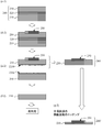
- FIG. 5 is a flowchart showing an example of a semiconductor wafer reuse process to which the present invention can be applied.
- a semiconductor wafer 110 is prepared as shown in FIG. 5A (step a-1).
- the semiconductor wafer 110 is not particularly limited as long as the porous layer can be formed by changing the wafer surface portion to the porous layer, but a p-type silicon single crystal wafer is preferably used as described above. Can be used.
- the wafer diameter is not particularly limited, and the present invention can be applied even to a wafer having a diameter of 450 mm or more.
- the thickness t 1 of the semiconductor wafer 110 to the preparation is not particularly limited, it is possible to use a wafer of normal standards.
- the porous layer 120 is formed on the surface 111 of the semiconductor wafer 110 by changing the surface portion of the semiconductor wafer 110 into a porous layer (step b-1).
- the formation of the porous layer 120 can be performed, for example, by an anodizing method, and the formation conditions (porosity, thickness, etc. of the porous layer 120) are appropriately selected so as to be convenient for peeling described later. be able to.
- the porous layer 120 can be formed in a plurality of stages, and the porous layer 120 can have a multilayer structure.
- the thickness of the porous layer 120 can be 1 to 10 ⁇ m, but is not limited thereto.
- the thickness t 2 of the semiconductor wafer 110 decreases from the thickness t 1 of the semiconductor wafer 110 prepared in step a-1 by the amount used for the change to the porous layer 120.
- a pretreatment may be performed before the step of forming the semiconductor film 130, which will be described later, so as to close the holes present on the surface of the porous layer 120 (pre-growth treatment— 1). It is preferable to perform such pretreatment because generation of defects in the semiconductor film 130 can be suppressed when the semiconductor film 130 is formed by epitaxial growth.
- a semiconductor film 130 is formed on the surface of the porous layer 120 to manufacture a semiconductor wafer 140 with a multilayer film (step c-1).
- the semiconductor film 130 can be formed with various properties (thickness, conductivity type, resistivity, etc.) suitable for the semiconductor device to be manufactured.
- the semiconductor film 130 can be formed by, for example, epitaxial growth. The epitaxial growth conditions can be selected as appropriate.
- the total thickness of the multilayer-coated semiconductor wafer 140 manufactured at this time is T.
- the element 150 is formed on the semiconductor film 130 (step d-1).
- Various kinds of elements 150 can be manufactured and are not particularly limited.
- back-illuminated devices among image sensors such as DRAM, NAND Flash, CCD / CIS, etc. that are being developed for Multi-Chip-Package (MCP), combinations of these image sensors and memories, and combinations of MPU and memories
- MCP Multi-Chip-Package
- the present invention is suitable for a device that requires a thin film, such as a three-dimensional device.
- the semiconductor film 130 on which the element 150 is manufactured is peeled off by the porous layer 120 to manufacture the semiconductor device 160 (step e-1).
- the peeling here can adopt a method that can be peeled off by the porous layer 120.
- a method of applying a jet of water to the porous layer 120 or a method of mechanically peeling can be employed.
- the element 150 side is preferably protected by being attached to a temporary attachment substrate (quartz substrate or the like) through wax or the like.
- an ultraviolet (UV) curable resist can be used instead of wax, and after the quartz substrate is temporarily attached, ultraviolet rays can be irradiated from the quartz substrate side to cure the resist and protect it.
- an appropriate method such as mechanical peeling other than a water jet can be adopted.
- a porous layer residual film 120b remains on the back surface of the semiconductor film 130 (the side opposite to the side on which the element 150 is formed). This is selected by etching. Can be removed. As an etchant, a mixed aqueous solution of HF / HNO 3 / CH 3 COOH or the like can be used.
- the protective means such as the quartz substrate of the element 150 as described above is preferably removed after the remaining film 120b of the porous layer is removed by etching.
- the surface on the porous layer 120 (porous film remaining film 120a) side used for peeling is flattened (step f). -1).
- the porous layer 120a on the surface as a remaining film is removed by etching or the like.
- the surface of the semiconductor wafer 110 on the side where the porous layer 120 (the remaining film 120a of the porous layer) is present is repolished.
- the residual film 120a of the porous layer can be removed by polishing in the same process as the polishing of the surface of the semiconductor wafer 110, instead of removing it alone.
- the semiconductor wafer 110 after peeling is flattened to form a semiconductor wafer 210, which is used as a semiconductor wafer to be reused.
- the thickness t 3 of the semiconductor wafer 210 to be reused is reduced by the flattening for reuse from the thickness t 2 after the porous layer is formed.
- the semiconductor wafer 210 to be reused in this way is again put into a process corresponding to FIG. 5A as a semiconductor wafer for forming a porous layer (step a-2), and a porous layer is formed (step b). -2) and the formation of the semiconductor film (step c-2) are performed again to manufacture a semiconductor wafer with a multilayer film again.
- the present invention includes a step of adjusting the thickness so that the entire thickness of the semiconductor wafer with a multilayer film manufactured using the semiconductor wafer 210 to be reused falls within a predetermined standard.
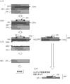
- FIG. 1 (a-1), (b-1), and (c-1) correspond to (a), (b), and (c) of FIG. 5, respectively, and the first cycle (reuse) Shows the first manufacturing process).
- FIGS. 1 (a-2), (b-2), and (c-2) show a second cycle (first manufacturing process using a semiconductor wafer to be reused).
- the semiconductor wafer 210 that has been planarized in the above-described step f-1 is used again as a semiconductor wafer for forming a porous layer (step a-2).
- the thickness of the semiconductor wafer 210 to be reused at this time is minute planarization for reuse is reduced, and is t 3, as described above. That is, the thickness of the wafer is reduced by t 1 -t 3 as compared with the semiconductor wafer 110 initially prepared in step a-1.
- the planarized surface 211 of the semiconductor wafer 210 is changed to a porous layer to form the porous layer 220 (step b-2).
- the formation of the porous layer 220 can be performed using the same method as in the formation of the porous layer 120 in step b-1.
- the thickness t 4 of the semiconductor wafer 210 decreases from the thickness t 3 of the semiconductor wafer 210 prepared for reuse in the step a-2 by the amount used for the change to the porous layer 220.
- a pre-growth treatment step similar to the pre-growth treatment 1 performed before the first growth of the semiconductor layer can be performed (pre-growth treatment-2).
- a semiconductor film 230 is formed on the surface of the porous layer 220 to manufacture a semiconductor wafer 240 with a multilayer film (step c-2).
- the formation of the semiconductor film 230 can be performed using a method similar to that for forming the semiconductor film 130 in Step c-1.
- the thickness of the semiconductor film 230 formed on the surface of the porous layer 220 the entire thickness of the semiconductor wafer 240 with the multilayer film is within a predetermined standard. It is possible to adjust the thickness.
- the total thickness of the semiconductor wafer 210 to be reused after peeling at the time of step a-2 is such that the thickness of the wafer is t 1 -t 3 compared to the semiconductor wafer 110 initially prepared in step a-1. (Specifically, for example, at least about a few ⁇ m as described above), it is manufactured by forming the semiconductor film 230 to be thick so as to compensate for the decrease in the semiconductor wafer. Variation in thickness of the semiconductor wafer with multilayer film, that is, variation in thickness between the semiconductor wafer 140 with multilayer film manufactured in the first cycle and the semiconductor wafer 240 with multilayer film manufactured in the second cycle is reduced. Can do. The allowable range (allowable tolerance) of this variation in thickness varies depending on the device to be manufactured, but if the reproduction process is repeated without adjusting the thickness, it will eventually exceed the allowable range.
- FIG. 2 (c-2) corresponds to FIG. 1 (c-2), and a semiconductor wafer 240 with a multilayer film manufactured by forming the semiconductor film 230 thick on the surface of the porous layer 220 by t 1 -t 3 is shown. (Step c-2).
- an element 250 is formed on the semiconductor film 230 by the same method as in step d-1 (FIG. 5 (d)).
- Step d-2 With respect to this semiconductor wafer 240 with a multilayer film, as shown in FIG. 2 (d-2), an element 250 is formed on the semiconductor film 230 by the same method as in step d-1 (FIG. 5 (d)). Step d-2).
- the semiconductor film 230 on which the element 250 is fabricated is peeled off by the porous layer 220 by the same method as in the step e-1 (FIG. 5 (e)).
- the device 260 is manufactured (step e-2).
- the thickness of the semiconductor film 230 to be formed in the step c-2 is determined by the type of the element to be manufactured, as described above, the thickness of the semiconductor layer 230 is larger than that of the semiconductor layer 130 in the first cycle.
- the thickness is increased by t 1 -t 3 (for example, about several tens of ⁇ m), there is a concern that inconvenience may occur in manufacturing the device. Therefore, after the peeling, if necessary, the peeling surface side of the semiconductor film 230 can be removed by etching together with the remaining film 220b of the porous layer to adjust the film thickness (see FIG. 2 (g-2)).
- Semiconductor device 260 ′ shown.
- the semiconductor wafer 210 after peeling As shown in FIG. 2 (f-2), the surface on the porous layer 220 (porous film residual film 220a) side used for peeling is formed on the step f-1 (FIG. 5).
- planarization is performed (step f-2) to obtain a semiconductor wafer 310, which is used as a semiconductor wafer 310 to be reused.
- the third and subsequent cycles can be performed, and the semiconductor wafer after peeling can be reused to manufacture a semiconductor wafer with a multilayer film and a semiconductor device.
- the formation of the semiconductor film is mainly performed by a technique such as epitaxial growth.
- a technique such as epitaxial growth.
- the thickness of the semiconductor device mainly targeted by the present invention is, for example, a semiconductor film of about 20 to 100 ⁇ m including the support layer that supports the active layer with mechanical strength. Since the epitaxial growth rate is several ⁇ m / min or more, even if an extra thickness of 10 tens ⁇ m to several tens of ⁇ m is deposited, the reaction time at the time of epitaxial growth is only extended by several minutes. The cost increase of the process does not have to be so large.
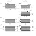
- FIG. 3 shows another example of a method for adjusting the thickness of the semiconductor film 230.
- (C-3) to (g-3) in FIG. 3 correspond to (c-2) to (g-2) in FIG. 2, respectively.
- the etching is performed by providing an etching removal region 230a on the porous layer 220 side of the semiconductor film 230 formed on the surface of the porous layer 220.
- the etching removal region 230a referred to here is a layer serving as a margin for removal by etching after peeling in order to adjust the thickness of a semiconductor device to be manufactured.
- the entire semiconductor film can be formed as a uniform layer, and a predetermined thickness of the semiconductor film can be used as an etching removal region.
- the etching removal region 230a has an etching rate higher than that of a layer left without etching removal. It is preferable to form a fast layer.
- the semiconductor device 260 ′ can be obtained by performing the etching removal more quickly and accurately.
- a p + layer (with a resistivity of about 0.01 ⁇ cm) is formed as the etching removal region 230a
- a p ⁇ layer (a lightly doped layer, with a resistivity of about 10 ⁇ cm) is formed as a layer that remains without being etched away
- the semiconductor wafer 240 with a multilayer film having the etching removal region 230a on the porous layer 220 side of the semiconductor film 230 as described above the semiconductor wafer with a multilayer film having an overall thickness within the standard can be obtained at low cost. Can be provided.
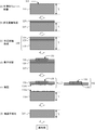
- the additional film 270 is formed on the surface opposite to the surface 211 forming the porous layer 220 of the semiconductor wafer 210 (see FIG. 4A-4) to be reused in the second cycle.
- the thickness adjustment is performed so that the entire thickness of the semiconductor wafer 240 with a multilayer film falls within a predetermined standard.
- the thickness of the additional film 270 can be t 1 -t 3 .
- the material of the additional film 270 on the back surface may be the same as that of the semiconductor wafer 210 to be reused, the dopant concentration may be changed, or a polycrystalline film may be used. If a polycrystalline film is formed as the additional film 270 on the back surface, it can be formed at a low cost, and an effect of functioning as a gettering layer for contaminants such as metal impurities at the time of heat treatment such as a subsequent element formation process can be obtained. It is preferable because it is possible.
- the porous layer 220 is formed (step b-4), and the semiconductor film 230 is formed (step c-4).
- a semiconductor wafer 240 with a porous film having a thickness T can be obtained.
- the entire thickness of the semiconductor wafer 240 with a multilayer film is formed by forming an additional film on the surface opposite to the surface on which the porous layer of the semiconductor wafer to be reused is formed.
- the thickness can be adjusted so as to fall within a predetermined standard.
- the thickness adjustment for forming the additional film on the back surface of the wafer is performed every time the semiconductor wafer is reused (every cycle), but the thickness after the reuse is repeated several times. You may make it adjust a decreasing part collectively. This is preferable because a cost reduction effect can be easily obtained.
- the additional film 270 ′ is formed on the surface 211 ′ on the side on which the porous layer 220 is formed of the semiconductor wafer 210 (see FIG. 6A-5) to be reused in the second cycle.
- the thickness adjustment is performed so that the entire thickness of the semiconductor wafer 240 with the multilayer film falls within a predetermined standard.
- the thickness of the additional film 270 ′ can be, for example, t 1 ⁇ t 3 .
- the additional film 270 ′ needs to be made of a material that can be changed into a porous layer, and constitutes a semiconductor wafer together with the semiconductor wafer 210 to be reused.
- the conductivity type, resistivity, and the like of the additional film 270 ′ are not necessarily the same as those of the semiconductor wafer 210 to be reused, and can be adjusted as appropriate.
- the surface portion of the additional film 270 ′ (that is, the surface portion of the semiconductor wafer) constituting the semiconductor wafer together with the semiconductor wafer 210 to be reused is made porous.
- the porous layer 220 is formed on the surface 271 of the additional film 270 ′ (step b-5).
- FIG. 6B-5 shows a case where a part of the additional film 270 ′ remains, but the present invention is not limited to this.
- a part of the reused semiconductor wafer 210 is changed into a porous layer. May be.
- a semiconductor film 230 with a thickness T can be obtained by forming a semiconductor film 230 on the surface of the porous layer 220 (step c). -5).
- the total thickness of the semiconductor wafer 240 with a multilayer film is predetermined. The thickness can be adjusted to be within the specifications.
- the thickness may be adjusted by forming an additional film, but the thickness reduction after repeated reuse may be adjusted collectively. In this way, it is preferable to adjust the thickness reduction after the reuse is repeated several times so that the cost reduction effect can be easily obtained.
- a wafer having a diameter of 450 mm which has been developed as a next generation wafer of a silicon single crystal wafer having a diameter of 300 mm, or a semiconductor wafer having a larger diameter than that can be preferably used.
- the deflection of the wafer due to its own weight becomes a problem.
- the wafer thickness is about 1.5 to 2 mm or more in order to sufficiently suppress the deflection. It is estimated that it is necessary to.
- the raw material cost is further increased if the usage method is used up once in the conventional device fabrication.
- the method of reusing the semiconductor wafer of the present invention as described above, even when a standard where the wafer thickness is significantly thicker than the conventional one is required for suppressing the deflection of the wafer, The peeling semiconductor wafer can be reused many times with a thickness corresponding to the standard, and the cost can be reduced.
- Example 2 A semiconductor wafer with a multilayer film and a semiconductor device were manufactured according to the method for manufacturing a semiconductor wafer with a multilayer film and the method for manufacturing a semiconductor device of the present invention shown in FIGS. This will be described with reference to FIG.
- a porous layer 120 was formed on one surface 111 (step b-1).
- the entire thickness of the porous layer 120 is 9 ⁇ m. Therefore, the thickness t 2 of the semiconductor wafer 110 at this time is about 736 ⁇ m.
- pores on the surface of the porous layer 120 are closed to suppress generation of defects in the epitaxial layer (semiconductor film 130) grown on the porous layer 120.
- the following treatment was performed (pre-growth treatment-1).
- side wall oxidation of the pores of the porous layer 120 was performed at 400 ° C. for 1 hour in an oxygen atmosphere.
- the oxide film on the surface of the porous layer 120 was etched with hydrofluoric acid (HF aqueous solution).
- pre-baking was performed at 950 ° C. in a hydrogen atmosphere. Thereafter, hydrogen gas baking containing dilute Si gas was performed.
- a semiconductor film 130 was formed on the surface of the porous layer 120 by epitaxial growth as follows (step c-1).
- the epitaxial growth conditions were such that the atmospheric gas was SiHCl 3 (trichlorosilane) / H 2 , the temperature was 1150 ° C., the dopant was boron, and the growth rate was 3 ⁇ m / min.
- the thickness of the semiconductor film 130 after epitaxial growth was 30 ⁇ m, the conductivity type of the semiconductor film 130 was p-type, and the resistivity was 10 ⁇ cm.
- the total thickness T of the wafer after epitaxial growth was 775 ⁇ m.
- a dummy CCD device was fabricated as an element 150 on the semiconductor film 130 (step d-1).
- the porous layer 120 was peeled as follows to separate the semiconductor film 130 from which the element 150 was produced from the semiconductor wafer 110 (step e-1). Specifically, the surface of the element 150 was covered with wax and then attached to a temporary attachment quartz substrate. Thereafter, the porous layer 120 was peeled off by applying a water jet. On the peeled element 150 and semiconductor film 130 side, the quartz substrate temporarily attached was removed by removing the wax. Further, the remaining film 120b of the porous layer on the back surface (the side opposite to the side on which the element 150 is formed) is removed by etching using a mixed aqueous solution of HF / HNO 3 / CH 3 COOH as an etching solution, thereby removing the semiconductor device. 160.
- the porous layer 120a on the surface as a residual film was removed by etching using HF / HNO 3 / CH 3 COOH as an etchant. Thereafter, the surface of the semiconductor wafer 110 where the porous layer was present was repolished (step f-1). The back surface (the surface opposite to the side where the porous layer was present) was also polished. In this way, a process for reuse was performed, and a semiconductor wafer (recycled wafer) 210 to be reused was obtained. The total reclaiming allowance including the back surface was 5 ⁇ m.
- the thickness t 3 of the semiconductor wafer 210 to be reused that has been subjected to the planarization process was 731 ⁇ m. That is, it decreased by 14 ⁇ m with respect to the original semiconductor wafer 110.
- the flattened semiconductor wafer 210 was prepared for use as a semiconductor wafer for forming a porous layer again (see FIG. 1 (a-2), step a-2).
- the surface 211 of the flattened semiconductor wafer 210 is changed into a porous layer by anodization to form a porous layer 220 (step b-2).
- the second porous layer 220 was formed under the same conditions as the first porous layer formation (step b-1).
- the thickness of the porous layer 220 was 9 ⁇ m, and the thickness t 4 of the semiconductor wafer 210 at this time was about 722 ⁇ m.
- a pre-growth treatment step was performed under the same conditions as the pre-growth treatment-1 performed before the first semiconductor layer growth (growth pre-treatment-2).
- a semiconductor film 230 was formed on the surface of the porous layer 220 by epitaxial growth as follows (step c-3). At this time, as shown in FIG. 3C-3, an etching removal region 230a was provided on the porous layer 220 side of the semiconductor film 230.
- the specific method for forming the semiconductor film 230 is as follows. Epitaxial growth was performed in two stages with different conditions.
- the epitaxial growth conditions were such that the atmospheric gas was SiHCl 3 (trichlorosilane) / H 2 , the temperature was 1150 ° C., the dopant was boron, and the growth rate was 3 ⁇ m / min.
- the thickness of the first epitaxial layer (corresponding to the etching removal region 230a) is 14 ⁇ m (that is, corresponding to the total thickness reduction of the recycled wafer 210 from the original semiconductor wafer 110), the conductivity type is p-type, and the resistivity
- the growth time and the dopant concentration were set to 0.012 ⁇ cm (p + layer, ie, the dopant was highly concentrated).
- a dummy CCD device was fabricated as an element 250 on the semiconductor film 230 in the same manner as in step d-1 (step d-3).
- the surface of the element 250 is protected with wax and a temporary sticking quartz substrate by the same method as in the step e-1, and then the water jet is applied to the porous layer 220.
- the semiconductor film 230 on which the element 250 peeled off was applied and the semiconductor wafer 210 were separated (step e-3).
- the remaining film 220b of the porous layer is removed by etching to form the semiconductor device 260.
- the wax on the element 250 side and the temporarily attached quartz substrate were removed to obtain a semiconductor device 260 ′ from which the etching removal region 230a was removed.
- the peeled semiconductor wafer 210 is etched away from the porous layer 220a on the surface as a residual film by the same method as in the step f-1. Both surfaces were polished to obtain a semiconductor wafer 310 to be reused (step f-3).
- the present invention is not limited to the above embodiment.
- the above embodiment is merely an example, and the present invention has the same configuration as that of the technical idea described in the claims of the present invention, and any device that exhibits the same function and effect is the present invention. It is included in the technical scope of the invention.
Landscapes
- Recrystallisation Techniques (AREA)
- Weting (AREA)
- Mechanical Treatment Of Semiconductor (AREA)
Abstract
本発明は、表面部を多孔質層に変化させることにより半導体ウェーハの表面に多孔質層を形成、多孔質層上に半導体膜を形成して多層膜付き半導体ウェーハを製造、半導体膜上に素子を作製、及び、多孔質層で剥離して半導体デバイスを製造、の各工程により半導体デバイスを製造する際に、剥離後の半導体ウェーハを平坦化し、平坦化を行った半導体ウェーハを再利用して多層膜付き半導体ウェーハを製造する方法であって、再利用する半導体ウェーハを用いて製造された多層膜付き半導体ウェーハの全体の厚さが所定の規格内に入るように厚さ調整を行う工程を含む多層膜付き半導体ウェーハの製造方法である。これにより、剥離用半導体ウェーハに多孔質層を形成する方法を採用して半導体デバイス作製用の多層膜付き半導体ウェーハを製造する際、剥離用半導体ウェーハの再利用回数にかかわらず、規格内の全体厚さを有する多層膜付き半導体ウェーハが低コストで提供される。
Description
本発明は、半導体ウェーハ上に多孔質層と半導体膜とを有する多層膜付き半導体ウェーハ及びその製造方法、並びに、そのような多層膜付き半導体ウェーハを用いて半導体デバイスを製造する方法に関する。
ICカードなどに使用される薄膜半導体デバイスを製造する方法として、特許文献1に記載されているように、半導体ウェーハ表面に多孔質層を形成し、その多孔質層の表面に素子形成領域となる半導体膜を形成したウェーハを作製し、その半導体膜上に素子を形成した後に多孔質層で剥離して薄膜半導体デバイスを形成する方法がある。
この方法によれば、剥離により薄膜化を行うために、素子を形成した後の半導体ウェーハの裏面側(デバイスを作製する側とは反対側)を従来のように研削・研磨等で除去する必要がなく、その結果、材料ロスが少なく、削り屑などの廃棄物も低減できるため、環境面でのメリットが得られる。さらに、剥離後の半導体ウェーハを再利用することにより、使用する製品ウェーハの枚数を減らすことができるため、製造コストを削減できるというメリットが大いに期待されている。
しかし、この半導体ウェーハを再利用するに当たっては、多孔質層で剥離(分離)するので、剥離面(分離面)には微小な割れ欠けが生じており、このため、このような剥離面を有する多孔質層を全て除去し、あらためて多孔質層を形成する必要がある。したがって、ウェーハの厚みは、ウェーハを再生する毎に少なくとも多孔質層の厚み分が薄くなるという問題があった。
このように、再利用する半導体ウェーハがウェーハを再生する毎に薄くなると、半導体デバイスを作製するウェーハの全体厚も薄くなるため、再利用する回数が増加すると、デバイス作製の際のウェーハ全体厚の規格値から外れ、デバイス製造工程に投入することができなくなる。そのため、ウェーハの再利用回数が制限されるという問題があった。
本発明は、前記問題点を解決するためになされたものであって、剥離用半導体ウェーハに多孔質層を形成する方法を採用して半導体デバイス作製用の多層膜付き半導体ウェーハを製造する際、剥離用半導体ウェーハの再利用回数にかかわらず、規格内の全体厚さを有する多層膜付き半導体ウェーハを提供することを目的とする。
上記目的達成のため、本発明は、少なくとも、半導体ウェーハの表面部を多孔質層に変化させることにより半導体ウェーハの表面に多孔質層を形成する工程と、該多孔質層の表面上に半導体膜を形成して多層膜付き半導体ウェーハを製造する工程と、前記半導体膜上に素子を作製する工程と、該素子を作製した半導体膜を前記多孔質層で剥離して半導体デバイスを製造する工程とにより、半導体デバイスを製造する際に、前記素子が作製された半導体膜を剥離した後の半導体ウェーハの前記剥離に用いた多孔質層側の表面を平坦化する工程を行い、該平坦化を行った半導体ウェーハを、前記多孔質層を形成するための半導体ウェーハとして再利用し、前記多孔質層の形成工程と、前記半導体膜の形成工程とを行って多層膜付き半導体ウェーハを製造する方法であって、前記再利用する半導体ウェーハを用いて製造された前記多層膜付き半導体ウェーハの全体の厚さが、所定の規格内に入るように厚さ調整を行う工程を含むことを特徴とする多層膜付き半導体ウェーハの製造方法を提供する。
このような工程を有し、剥離用半導体ウェーハを再利用する多層膜付き半導体ウェーハの製造方法であれば、剥離用半導体ウェーハの再利用回数にかかわらず、規格内の全体厚さを有する多層膜付き半導体ウェーハを提供することができる。
この場合、前記厚さ調整を、前記再利用する半導体ウェーハの表面に多孔質層を形成した後に、該多孔質層の表面上に形成する半導体膜の厚さを調整することにより行うことができる。
このように、再利用する半導体ウェーハの表面に多孔質層を形成した後に、該多孔質層の表面上に形成する半導体膜の厚さを調整することにより、規格内の全体厚さを有する多層膜付き半導体ウェーハを提供することができる。
このように、再利用する半導体ウェーハの表面に多孔質層を形成した後に、該多孔質層の表面上に形成する半導体膜の厚さを調整することにより、規格内の全体厚さを有する多層膜付き半導体ウェーハを提供することができる。
さらにこの場合、前記多孔質層の表面上に形成する半導体膜の前記多孔質層側にエッチング除去用領域を設けることが好ましい。
なお、ここで言うエッチング除去用領域とは、作製する半導体デバイスの厚さを調整するため、剥離後にエッチングによって除去するための取り代となる層のことである。また、半導体デバイスの厚さとは、半導体デバイスの電気的活性層と、その活性層を機械的強度で支える支持層とを合わせた厚さのことである。半導体膜全体を均一の層で形成してそのうちの所定厚さをエッチング除去用の領域とすることもできるが、エッチング除去用領域としては、エッチング除去せずに残す層に比べてエッチング速度が速い層を形成することが好ましい。
このように、多孔質層の表面上に形成する半導体膜の多孔質層側にエッチング除去用領域を設ければ、より速く正確にエッチング除去を行うことができる。
なお、ここで言うエッチング除去用領域とは、作製する半導体デバイスの厚さを調整するため、剥離後にエッチングによって除去するための取り代となる層のことである。また、半導体デバイスの厚さとは、半導体デバイスの電気的活性層と、その活性層を機械的強度で支える支持層とを合わせた厚さのことである。半導体膜全体を均一の層で形成してそのうちの所定厚さをエッチング除去用の領域とすることもできるが、エッチング除去用領域としては、エッチング除去せずに残す層に比べてエッチング速度が速い層を形成することが好ましい。
このように、多孔質層の表面上に形成する半導体膜の多孔質層側にエッチング除去用領域を設ければ、より速く正確にエッチング除去を行うことができる。
また、前記厚さ調整を、前記素子が作製された半導体膜を剥離した後に、前記再利用する半導体ウェーハの表面上に付加膜を形成することにより行うことができる。
この場合、前記付加膜を、前記再利用する半導体ウェーハの多孔質層を形成する表面上に形成することができる。また、前記付加膜を、前記再利用する半導体ウェーハの多孔質層を形成する表面とは反対側の表面上に形成することもできる。
この場合、前記付加膜を、前記再利用する半導体ウェーハの多孔質層を形成する表面上に形成することができる。また、前記付加膜を、前記再利用する半導体ウェーハの多孔質層を形成する表面とは反対側の表面上に形成することもできる。
このように、素子が作製された半導体膜を剥離した後に、前記再利用する半導体ウェーハの表面上に付加膜を形成することによっても、多層膜付き半導体ウェーハの厚さ調整を行うことができ、規格内の全体厚さを有する多層膜付き半導体ウェーハを提供することができる。また、この付加膜は、再利用する半導体ウェーハの多孔質層を形成する表面上、及びその反対側の表面上のいずれにも形成することができる。
さらに、付加膜を再利用する半導体ウェーハの多孔質層を形成する表面とは反対側の表面上に形成する場合、前記付加膜として、多結晶膜を形成することができる。
このように、裏面の付加膜として多結晶膜を形成すれば、安価である上に、その後の素子形成工程等の熱処理時に金属不純物等の汚染物のゲッタリング層として機能する効果を得ることができる。
このように、裏面の付加膜として多結晶膜を形成すれば、安価である上に、その後の素子形成工程等の熱処理時に金属不純物等の汚染物のゲッタリング層として機能する効果を得ることができる。
また、本発明は、上記のいずれかの多層膜付き半導体ウェーハの製造方法により製造された多層膜付き半導体ウェーハの半導体膜上に素子を作製する工程と、該素子を作製した半導体膜を前記多孔質層で剥離して半導体デバイスを製造する工程とを有することを特徴とする半導体デバイスの製造方法を提供する。
このような半導体デバイスの製造方法であれば、規格内の全体厚さを有する多層膜付き半導体ウェーハを使用できるので、再利用回数の制限なく半導体デバイスを製造することができる。
このような半導体デバイスの製造方法であれば、規格内の全体厚さを有する多層膜付き半導体ウェーハを使用できるので、再利用回数の制限なく半導体デバイスを製造することができる。
また、本発明は、半導体ウェーハと、該半導体ウェーハの表面に形成された多孔質層と、該多孔質層の表面上に形成された半導体膜とを有する、半導体デバイス製造用の多層膜付き半導体ウェーハであって、前記半導体膜は、前記多孔質層側にエッチング除去用領域を有することを特徴とする多層膜付き半導体ウェーハを提供する。
このようなエッチング除去用領域を有する多層膜付き半導体ウェーハであれば、低コストで提供できる規格内の全体厚さを有する多層膜付き半導体ウェーハとすることができる。
このようなエッチング除去用領域を有する多層膜付き半導体ウェーハであれば、低コストで提供できる規格内の全体厚さを有する多層膜付き半導体ウェーハとすることができる。
この場合、半導体ウェーハの直径が450mm以上の場合に極めて有効である。
このように、半導体ウェーハの直径が450mm以上のような大直径のウェーハであり、自重によるウェーハのたわみが問題となり、ウェーハの厚みを比較的厚くする必要がある場合であっても、ウェーハのたわみに対応できる充分厚い厚さでウェーハを設計しても剥離用の半導体ウェーハを何度も再利用することができ、低コストとすることができる。
このように、半導体ウェーハの直径が450mm以上のような大直径のウェーハであり、自重によるウェーハのたわみが問題となり、ウェーハの厚みを比較的厚くする必要がある場合であっても、ウェーハのたわみに対応できる充分厚い厚さでウェーハを設計しても剥離用の半導体ウェーハを何度も再利用することができ、低コストとすることができる。
本発明の多層膜付き半導体ウェーハの製造方法に従えば、剥離用半導体ウェーハに多孔質層を形成する方法を採用して半導体デバイス作製用の多層膜付き半導体ウェーハを製造する際、剥離用ウェーハの再利用回数にかかわらず、規格内の全体厚さを有する多層膜付き半導体ウェーハを提供することができる。
また、本発明の半導体デバイスの製造方法に従えば、規格内の全体厚さを有する多層膜付き半導体ウェーハを使用できるので、再利用回数の制限なく、半導体デバイスを製造することができる。
また、本発明に係る多層膜付き半導体ウェーハであれば、低コストで提供できる規格内の全体厚さを有する多層膜付き半導体ウェーハとすることができる。
また、本発明の半導体デバイスの製造方法に従えば、規格内の全体厚さを有する多層膜付き半導体ウェーハを使用できるので、再利用回数の制限なく、半導体デバイスを製造することができる。
また、本発明に係る多層膜付き半導体ウェーハであれば、低コストで提供できる規格内の全体厚さを有する多層膜付き半導体ウェーハとすることができる。
以下、本発明を詳細に説明するが、本発明はこれらに限定されるものではない。
前述のように、半導体ウェーハ表面に多孔質層を形成する方法を採用した場合、再利用回数が増えるたびにウェーハ厚さが薄くなってしまうという問題があった。
前述のように、半導体ウェーハ表面に多孔質層を形成する方法を採用した場合、再利用回数が増えるたびにウェーハ厚さが薄くなってしまうという問題があった。
すなわち、剥離を行うために形成される多孔質層は、少なくとも数μm程度の厚さが必要であり、それに加えて、剥離後の半導体ウェーハ表面に残る多孔質層の除去と、ウェーハ表面を平坦化する処理を行うため数μm程度の研磨が必要とされる。つまり、一回の再生処理で初期半導体ウェーハの厚さが少なくとも10μm程度薄くなってしまう。
その一方で、デバイス製造メーカーがデバイスを製造するためにウェーハ材料に要求するウェーハ厚の規格(公差)は、一般的には±15μm程度であり、製造するデバイスの種類によって規格が緩やかな場合であっても±25μm程度である。従って、ウェーハの全体厚から許容される剥離用半導体ウェーハの再利用回数は、許容公差を最大限利用しても±15μmの場合は2~3回以下、±25μmの場合は3~4回程度以下に限定されてしまうことになる。
本発明者らがコスト試算を行うと、例えばp+型のシリコン単結晶ウェーハを使用して多孔質層を形成する方法を採用した場合、再利用回数としては、少なくとも3回、好ましくは5回以上に設定しないと十分なコストメリットが得られないことが判明した。
本発明者らは、これらの知見に基づいてさらに検討を行い、剥離用半導体ウェーハに多孔質層を形成する方法を採用して半導体デバイス作製用の多層膜付き半導体ウェーハを製造する際には、再利用する半導体ウェーハを用いて製造された多層膜付き半導体ウェーハの全体の厚さが所定の規格内に入るように厚さ調整を行えば、剥離用ウェーハの再利用回数にかかわらず、規格内の全体厚さを有する多層膜付き半導体ウェーハを得ることができることに想到した。そして、そのような多層膜付き半導体ウェーハであれば、再利用回数にかかわらずデバイス製造工程に投入することができるため、多層膜付き半導体ウェーハの製造コストや、それを用いて製造されるデバイスの製造コストの低減効果が得られることに想到し、本発明を完成させた。
以下、本発明について図面を参照しながらさらに詳細に説明するが、本発明はこれらに限定されるものではない。特に、以下では繰り返して使用する剥離用半導体ウェーハとして、好適に用いることができるp型シリコン単結晶ウェーハを用いた場合について述べるが、本発明はこれに限定されず、その他の半導体ウェーハに適用することもできる。
図5に、本発明が適用することができる、半導体ウェーハの再利用のプロセスの一例を示すフローチャートを示す。
まず、再利用する前の1回目の製造プロセスとして、図5(a)に示すように、半導体ウェーハ110を準備する(工程a-1)。
半導体ウェーハ110としては、ウェーハ表面部を多孔質層に変化させることにより多孔質層を形成することができるものであれば特に限定されないが、上記のようにp型のシリコン単結晶ウェーハを好適に用いることができる。また、ウェーハ直径も特に限定されず、特に直径450mm以上のウェーハであっても本発明を適用することができる。
この準備する半導体ウェーハ110の厚さt1も特に限定されず、通常の規格のウェーハを用いることができる。
まず、再利用する前の1回目の製造プロセスとして、図5(a)に示すように、半導体ウェーハ110を準備する(工程a-1)。
半導体ウェーハ110としては、ウェーハ表面部を多孔質層に変化させることにより多孔質層を形成することができるものであれば特に限定されないが、上記のようにp型のシリコン単結晶ウェーハを好適に用いることができる。また、ウェーハ直径も特に限定されず、特に直径450mm以上のウェーハであっても本発明を適用することができる。
この準備する半導体ウェーハ110の厚さt1も特に限定されず、通常の規格のウェーハを用いることができる。
次に、図5(b)に示すように、半導体ウェーハ110の表面部を多孔質層に変化させることにより半導体ウェーハ110の表面111に多孔質層120を形成する(工程b-1)。
この多孔質層120の形成は、例えば陽極化成法によって行うことができ、その形成条件(多孔質層120の多孔度、厚さ等)は後述する剥離の際に都合が良いように適宜選択することができる。例えば、多孔質層120の形成を複数段階にわけて行い、多孔質層120を多層構造とすることもできる。多孔質層120の厚さは1~10μmとできるがこれに限定されない。
この多孔質層120の形成は、例えば陽極化成法によって行うことができ、その形成条件(多孔質層120の多孔度、厚さ等)は後述する剥離の際に都合が良いように適宜選択することができる。例えば、多孔質層120の形成を複数段階にわけて行い、多孔質層120を多層構造とすることもできる。多孔質層120の厚さは1~10μmとできるがこれに限定されない。
この時点での半導体ウェーハ110の厚さt2は工程a-1で準備された半導体ウェーハ110の厚さt1から、多孔質層120への変化に供された分だけ減少する。
また、図5には記載していないが、後述する半導体膜130の形成工程の前に、多孔質層120の表面に存在する孔を塞ぐような前処理を行っても良い(成長前処理-1)。
このような前処理を行うと、半導体膜130の形成をエピタキシャル成長により行う場合などにおいて、半導体膜130での欠陥の発生を抑えることができるので好ましい。
このような前処理を行うと、半導体膜130の形成をエピタキシャル成長により行う場合などにおいて、半導体膜130での欠陥の発生を抑えることができるので好ましい。
次に、図5(c)に示すように、多孔質層120の表面上に半導体膜130を形成して多層膜付き半導体ウェーハ140を製造する(工程c-1)。
この半導体膜130は、製造しようとする半導体デバイスに適した様々の性質(厚さ、導電型、抵抗率等)のものを形成することができる。
また、この半導体膜130は、例えば、エピタキシャル成長によって形成することができる。このエピタキシャル成長条件は適宜選択することができる。
この時点で製造した多層膜付き半導体ウェーハ140の全体の厚さをTとする。
この半導体膜130は、製造しようとする半導体デバイスに適した様々の性質(厚さ、導電型、抵抗率等)のものを形成することができる。
また、この半導体膜130は、例えば、エピタキシャル成長によって形成することができる。このエピタキシャル成長条件は適宜選択することができる。
この時点で製造した多層膜付き半導体ウェーハ140の全体の厚さをTとする。
次に、図5(d)に示すように、半導体膜130上に素子150を作製する(工程d-1)。
素子150としては様々な種類のものを作製することができ、特に限定されない。例えば、Multi-Chip-Package(MCP)用として開発が進んでいるDRAM、NAND Flash、CCD/CIS等の撮像素子のうち裏面照射型デバイス、またこれら撮像素子とメモリーの組み合わせやMPUとメモリーの組み合わせなど3次元化するデバイス等のような、チップの薄膜化が特に必要なものに本発明は好適である。
素子150としては様々な種類のものを作製することができ、特に限定されない。例えば、Multi-Chip-Package(MCP)用として開発が進んでいるDRAM、NAND Flash、CCD/CIS等の撮像素子のうち裏面照射型デバイス、またこれら撮像素子とメモリーの組み合わせやMPUとメモリーの組み合わせなど3次元化するデバイス等のような、チップの薄膜化が特に必要なものに本発明は好適である。
次に、図5(e)に示すように、素子150を作製した半導体膜130を多孔質層120で剥離して半導体デバイス160を製造する(工程e-1)。
ここでの剥離は多孔質層120で剥離できる方法を採用することができる。例えば、多孔質層120に水流のジェットを当てる方法や機械的に剥離する方法を採用することができる。
また、このとき、素子150側はワックス等を介して仮貼り付け用基板(石英基板など)に貼り付けて保護することが好ましい。また、ワックスの代わりに紫外線(UV)硬化レジストを用い、石英基板を仮貼り付け後、石英基板側より紫外線を照射し、レジスト硬化を行って保護することなどもできる。また、硬化後のレジストが水溶性の場合には水流ジェット以外の機械剥離を行うなど適切な方法を採用することができる。
ここでの剥離は多孔質層120で剥離できる方法を採用することができる。例えば、多孔質層120に水流のジェットを当てる方法や機械的に剥離する方法を採用することができる。
また、このとき、素子150側はワックス等を介して仮貼り付け用基板(石英基板など)に貼り付けて保護することが好ましい。また、ワックスの代わりに紫外線(UV)硬化レジストを用い、石英基板を仮貼り付け後、石英基板側より紫外線を照射し、レジスト硬化を行って保護することなどもできる。また、硬化後のレジストが水溶性の場合には水流ジェット以外の機械剥離を行うなど適切な方法を採用することができる。
なお、剥離後の素子150及び半導体膜130側には、半導体膜130の裏面(素子150が形成された側とは反対側)に多孔質層の残膜120bが残るが、これはエッチングにより選択的に除去することができる。エッチング液としてはHF/HNO3/CH3COOHの混合水溶液等を用いることができる。
前記したような素子150の石英基板などの保護手段は、この多孔質層の残膜120bのエッチング除去した後に除去することが好ましい。
前記したような素子150の石英基板などの保護手段は、この多孔質層の残膜120bのエッチング除去した後に除去することが好ましい。
もう一方の、剥離後の半導体ウェーハ110については、図5(f)に示すように、剥離に用いた多孔質層120(多孔質層の残膜120a)側の表面を平坦化する(工程f-1)。
まず残膜として表面にある多孔質層120aを、エッチング等により除去する。その後、半導体ウェーハ110の多孔質層120(多孔質層の残膜120a)のあった側の表面を再研磨する。
このとき、裏面(多孔質層のあった側とは反対側の表面)も研磨することが好ましい。また、両面研磨機を用いて両面を同時に研磨してもよい。
なお、多孔質層の残膜120aを単独で除去するのではなく、半導体ウェーハ110の表面の研磨と同一の工程で研磨して除去することもできる。
まず残膜として表面にある多孔質層120aを、エッチング等により除去する。その後、半導体ウェーハ110の多孔質層120(多孔質層の残膜120a)のあった側の表面を再研磨する。
このとき、裏面(多孔質層のあった側とは反対側の表面)も研磨することが好ましい。また、両面研磨機を用いて両面を同時に研磨してもよい。
なお、多孔質層の残膜120aを単独で除去するのではなく、半導体ウェーハ110の表面の研磨と同一の工程で研磨して除去することもできる。
このようにして剥離後の半導体ウェーハ110の平坦化を行って半導体ウェーハ210とし、これを再利用する半導体ウェーハとして用いる。
この時点で、再利用する半導体ウェーハ210の厚さt3は、多孔質層形成後の厚さt2から、再利用のための平坦化の分が減少している。
この時点で、再利用する半導体ウェーハ210の厚さt3は、多孔質層形成後の厚さt2から、再利用のための平坦化の分が減少している。
このようにして再利用する半導体ウェーハ210を再び多孔質層を形成するための半導体ウェーハとして図5(a)に相当するプロセスに投入し(工程a-2)、多孔質層の形成(工程b-2)と、半導体膜の形成(工程c-2)とを再度行って再度多層膜付き半導体ウェーハを製造する。このとき、本発明では、再利用する半導体ウェーハ210を用いて製造された多層膜付き半導体ウェーハの全体の厚さが、所定の規格内に入るように厚さ調整を行う工程を含む。
この多層膜付き半導体ウェーハの厚さ調整の具体的な態様の一例として、第一の態様を図1に示す。
図1(a-1)、(b-1)、及び(c-1)は、それぞれ、図5の(a)、(b)、(c)にそれぞれ相当し、1回目のサイクル(再利用する前の1回目の製造プロセス)を示す。一方、図1(a-2)、(b-2)、及び(c-2)は2回目のサイクル(再利用する半導体ウェーハを用いた1回目の製造プロセス)を示す。
図1(a-1)、(b-1)、及び(c-1)は、それぞれ、図5の(a)、(b)、(c)にそれぞれ相当し、1回目のサイクル(再利用する前の1回目の製造プロセス)を示す。一方、図1(a-2)、(b-2)、及び(c-2)は2回目のサイクル(再利用する半導体ウェーハを用いた1回目の製造プロセス)を示す。
前述の工程f-1で平坦化処理を行った半導体ウェーハ210を、図1(a-2)に示すように、再度多孔質層を形成するための半導体ウェーハとして利用する(工程a-2)。
この時点での再利用する半導体ウェーハ210の厚さは、再利用のための平坦化の分が減少しており、上記のようにt3になっている。すなわち、工程a-1で最初に準備した半導体ウェーハ110と比べて、ウェーハの厚さがt1-t3だけ減少している。
この時点での再利用する半導体ウェーハ210の厚さは、再利用のための平坦化の分が減少しており、上記のようにt3になっている。すなわち、工程a-1で最初に準備した半導体ウェーハ110と比べて、ウェーハの厚さがt1-t3だけ減少している。
次に、図1(b-2)に示すように、平坦化を行った半導体ウェーハ210の表面211を多孔質層に変化させ、多孔質層220を形成する(工程b-2)。
この多孔質層220の形成は、工程b-1の多孔質層120の形成の場合と同様の方法を用いて行うことができる。この時点での半導体ウェーハ210の厚さt4は工程a-2で再利用のため準備された半導体ウェーハ210の厚さt3から、多孔質層220への変化に供された分だけ減少する。
また多孔質層220を形成した後、前記した1回目の半導体層の成長前に行う成長前処理-1と同様の成長前処理工程を行うことができる(成長前処理-2)。
この多孔質層220の形成は、工程b-1の多孔質層120の形成の場合と同様の方法を用いて行うことができる。この時点での半導体ウェーハ210の厚さt4は工程a-2で再利用のため準備された半導体ウェーハ210の厚さt3から、多孔質層220への変化に供された分だけ減少する。
また多孔質層220を形成した後、前記した1回目の半導体層の成長前に行う成長前処理-1と同様の成長前処理工程を行うことができる(成長前処理-2)。
次に、図1(c-2)に示すように、多孔質層220の表面上に半導体膜230を形成して多層膜付き半導体ウェーハ240を製造する(工程c-2)。この半導体膜230の形成は、工程c-1の半導体膜130の形成の場合と同様の方法を用いて行うことができる。そして、このとき、多孔質層220の表面上に形成する半導体膜230の厚さを調整することにより行うことにより、多層膜付き半導体ウェーハ240の全体の厚さが、所定の規格内に入るように行う厚さ調整を行うことができる。
工程a-2の時点での剥離後の再利用する半導体ウェーハ210の全体の厚さは、工程a-1で最初に準備した半導体ウェーハ110と比べて、ウェーハの厚さがt1-t3だけ(具体的には、前述のように例えば少なくとも10数μm程度)減少しているので、半導体膜230を形成する際に半導体ウェーハの減少分を補償するように厚く形成することによって、製造された多層膜付き半導体ウェーハの厚さの変動、すなわち、1回目のサイクルで製造する多層膜付き半導体ウェーハ140と2回目のサイクルで製造する多層膜付き半導体ウェーハ240の厚さの変動を少なくすることができる。
尚、この厚さの変動の許容範囲(許容公差)は、作製するデバイスによっても異なるが、厚さ調整を行わずに再生処理を繰り返すと、いずれその許容範囲を超える事になる。
尚、この厚さの変動の許容範囲(許容公差)は、作製するデバイスによっても異なるが、厚さ調整を行わずに再生処理を繰り返すと、いずれその許容範囲を超える事になる。
半導体膜230の厚さを調整する方法の一例を図2に示す。
図2(c-2)は図1(c-2)に相当し、多孔質層220の表面上にt1-t3だけ厚く半導体膜230を形成して製造した多層膜付き半導体ウェーハ240を示している(工程c-2)。
図2(c-2)は図1(c-2)に相当し、多孔質層220の表面上にt1-t3だけ厚く半導体膜230を形成して製造した多層膜付き半導体ウェーハ240を示している(工程c-2)。
この多層膜付き半導体ウェーハ240に対し、図2(d-2)に示すように、工程d-1(図5(d))と同様の方法により、半導体膜230上に素子250を作製する(工程d-2)。
次に、図2(e-2)に示すように、工程e-1(図5(e))と同様の方法により、素子250を作製した半導体膜230を多孔質層220で剥離して半導体デバイス260を製造する(工程e-2)。
ところで、工程c-2で形成するべき半導体膜230の厚さは、作製する素子の種類によって決まるものであるため、前記のように、1回目のサイクルの半導体層130に比べて半導体層230の厚さをt1-t3だけ(例えば10数μm程度)厚く形成するとデバイス製造上不都合が生ずる懸念があるが、本発明が対象とする半導体デバイスの場合、半導体膜に素子を形成した後に剥離を行うので、その剥離後に、必要に応じて半導体膜230の剥離面側を、多孔質層の残膜220bとともにエッチング除去して膜厚を調整することができる(図2(g-2)に示す半導体デバイス260’)。
剥離後の半導体ウェーハ210については、図2(f-2)に示すように、剥離に用いた多孔質層220(多孔質層の残膜220a)側の表面を、工程f-1(図5(f))の場合と同様に平坦化を行って(工程f-2)半導体ウェーハ310とし、これを再利用する半導体ウェーハ310として用いる。
以上のようなサイクルを繰り返すことにより、3回目以降のサイクルも行うことができ、剥離後の半導体ウェーハを再利用し、多層膜付き半導体ウェーハ及び半導体デバイスを製造することができる。
以上のようなサイクルを繰り返すことにより、3回目以降のサイクルも行うことができ、剥離後の半導体ウェーハを再利用し、多層膜付き半導体ウェーハ及び半導体デバイスを製造することができる。
なお、半導体膜の形成は主にエピタキシャル成長等の手法により行われるが、上記のように、多層膜付き半導体ウェーハの厚さの変動を少なくするために半導体膜を厚く形成すると、エピタキシャル成長のコスト増加が懸念される。しかしながら、本発明が主に対象としている半導体デバイスの厚さは、活性層を機械的強度で支える支持層を含め、例えば20~100μm程度の半導体膜であって、その半導体膜を堆積する際のエピタキシャル成長速度は数μm/分あるいはそれ以上で行われるため、10数μm~数10μm分の厚さを余計に堆積したとしても、エピタキシャル成長時の反応時間を数分程度延長するだけであるため、エピタキシャル成長工程のコスト増加分はあまり大きくならずに済む。
次に、2回目のサイクルにおける半導体膜230の厚さを調整する方法の別の一例を説明する。
図3に半導体膜230の厚さを調整する方法の別の一例を示す。図3の(c-3)~(g-3)はそれぞれ図2の(c-2)~(g-2)に対応する。
図3に半導体膜230の厚さを調整する方法の別の一例を示す。図3の(c-3)~(g-3)はそれぞれ図2の(c-2)~(g-2)に対応する。
図3(c-3)に示したように、多孔質層220の表面上に形成する半導体膜230の、多孔質層220側にエッチング除去用領域230aを設けることにより行う。
なお、ここで言うエッチング除去用領域230aとは、作製する半導体デバイスの厚さを調整するため、剥離後にエッチングによって除去するための取り代となる層のことである。半導体膜全体を均一の層で形成してそのうちの所定厚さをエッチング除去用の領域とすることもできるが、エッチング除去用領域230aとしては、エッチング除去せずに残す層に比べてエッチング速度が速い層を形成することが好ましい。
このように、多孔質層の表面上に形成する半導体膜の多孔質層側にエッチング除去用領域を設ければ、より速く正確にエッチング除去を行って、半導体デバイス260’を得ることができる。
例えば、エッチング除去用領域230aとしてp+層(抵抗率0.01Ωcm程度)を形成し、エッチング除去せずに残す層としてp-層(低濃度ドープ層、抵抗率10Ωcm程度)を形成すれば、不純物濃度が高いほどエッチング速度が速くなるような選択エッチング液、例えば1-3-8エッチング液(HF(フッ化水素):HNO3(硝酸):CH3COOH(酢酸)=1:3:8の混酸)(特開平8-139297号公報参照)を用いてp+層を選択的にエッチング除去することができる。
なお、ここで言うエッチング除去用領域230aとは、作製する半導体デバイスの厚さを調整するため、剥離後にエッチングによって除去するための取り代となる層のことである。半導体膜全体を均一の層で形成してそのうちの所定厚さをエッチング除去用の領域とすることもできるが、エッチング除去用領域230aとしては、エッチング除去せずに残す層に比べてエッチング速度が速い層を形成することが好ましい。
このように、多孔質層の表面上に形成する半導体膜の多孔質層側にエッチング除去用領域を設ければ、より速く正確にエッチング除去を行って、半導体デバイス260’を得ることができる。
例えば、エッチング除去用領域230aとしてp+層(抵抗率0.01Ωcm程度)を形成し、エッチング除去せずに残す層としてp-層(低濃度ドープ層、抵抗率10Ωcm程度)を形成すれば、不純物濃度が高いほどエッチング速度が速くなるような選択エッチング液、例えば1-3-8エッチング液(HF(フッ化水素):HNO3(硝酸):CH3COOH(酢酸)=1:3:8の混酸)(特開平8-139297号公報参照)を用いてp+層を選択的にエッチング除去することができる。
上記したような、半導体膜230の多孔質層220側にエッチング除去用領域230aを有する多層膜付き半導体ウェーハ240であれば、規格内の全体厚さを有する多層膜付き半導体ウェーハを、低コストで提供することができる。
次に、本発明の多層膜付き半導体ウェーハの製造方法の別の一例として、第二の態様を、図4を参照して説明する。
この態様では、2回目のサイクルで再利用する半導体ウェーハ210(図4(a-4)参照)の多孔質層220を形成する表面211とは反対側の表面上に付加膜270を形成することにより、多層膜付き半導体ウェーハ240の全体の厚さが、所定の規格内に入るように厚さ調整を行う。付加膜270の厚さは、t1-t3とすることができる。
この態様では、2回目のサイクルで再利用する半導体ウェーハ210(図4(a-4)参照)の多孔質層220を形成する表面211とは反対側の表面上に付加膜270を形成することにより、多層膜付き半導体ウェーハ240の全体の厚さが、所定の規格内に入るように厚さ調整を行う。付加膜270の厚さは、t1-t3とすることができる。
この裏面の付加膜270の材質としては、再利用する半導体ウェーハ210と同じとしたり、ドーパント濃度を変えたりするなどしてもよく、また、多結晶膜とすることもできる。裏面の付加膜270として多結晶膜を形成すれば、安価に形成することができるし、その後の素子形成工程等の熱処理時に金属不純物等の汚染物のゲッタリング層として機能する効果を得ることができるので好ましい。
その後、図4(b-4)、(c-4)に示すように、多孔質層220を形成し(工程b-4)、半導体膜230を形成する(工程c-4)ことで、厚さTの多孔質膜付き半導体ウェーハ240を得ることができる。
また、3回目以降のサイクルでも同様に、再利用する半導体ウェーハの多孔質層を形成する表面とは反対側の表面上に付加膜を形成することにより、多層膜付き半導体ウェーハ240の全体の厚さが、所定の規格内に入るように厚さ調整を行うことができる。
なお、上記では半導体ウェーハの再利用のたびに(1回のサイクルごとに)ウェーハ裏面に付加膜を形成する厚さ調整を行う場合を示したが、再利用を数回繰り返した後の厚さ減少分を一括して調整するようにしてもよい。このようにすれば、コスト低減効果が得られやすくなり好ましい。
次に、本発明の多層膜付き半導体ウェーハの製造方法のさらに別の一例として、第三の態様を、図6を参照して説明する。
この態様では、2回目のサイクルで再利用する半導体ウェーハ210(図6(a-5)参照)の、多孔質層220を形成する側の表面211’上に付加膜270’を形成することにより、多層膜付き半導体ウェーハ240の全体の厚さが、所定の規格内に入るように厚さ調整を行う。付加膜270’の厚さは、例えばt1-t3とすることができる。
この態様では、2回目のサイクルで再利用する半導体ウェーハ210(図6(a-5)参照)の、多孔質層220を形成する側の表面211’上に付加膜270’を形成することにより、多層膜付き半導体ウェーハ240の全体の厚さが、所定の規格内に入るように厚さ調整を行う。付加膜270’の厚さは、例えばt1-t3とすることができる。
なお、この態様では、付加膜270’は多孔質層に変化させられる材質であることが必要であり、再利用する半導体ウェーハ210と一体となって半導体ウェーハを構成する。この場合、付加膜270’の導電型や抵抗率等は必ずしも再利用する半導体ウェーハ210と同じとする必要はなく、適宜調節することができる。
次に、図6(b-5)に示すように、再利用する半導体ウェーハ210と一体となって半導体ウェーハを構成する、付加膜270’の表面部(すなわち、半導体ウェーハの表面部)を多孔質層に変化させることにより付加膜270’の表面271に多孔質層220を形成する(工程b-5)。
なお、図6(b-5)では付加膜270’の一部が残る場合を示しているが、これに限定されず、例えば、再利用した半導体ウェーハ210の一部まで多孔質層に変化させてもよい。
なお、図6(b-5)では付加膜270’の一部が残る場合を示しているが、これに限定されず、例えば、再利用した半導体ウェーハ210の一部まで多孔質層に変化させてもよい。
その後、図6(c-5)に示すように、多孔質層220の表面上に半導体膜230を形成することで、厚さTの多孔質膜付き半導体ウェーハ240を得ることができる(工程c-5)。
また、3回目以降のサイクルでも同様に、再利用する半導体ウェーハの多孔質層を形成する側の表面上に付加膜を形成することにより、多層膜付き半導体ウェーハ240の全体の厚さが、所定の規格内に入るように厚さ調整を行うことができる。
なお、このように付加膜の形成を再利用する半導体ウェーハの多孔質層を形成する表面上に行う場合についても、上記のように半導体ウェーハの再利用のたびに(1回のサイクルごとに)付加膜を形成して厚さ調整を行ってもよいが、再利用を数回繰り返した後の厚さ減少分を一括して調整するようにしてもよい。このように再利用を数回繰り返した後の厚さ減少分を一括して調整するようにすれば、コスト低減効果が得られやすくなり好ましい。
また、本発明では、直径300mmのシリコン単結晶ウェーハの次世代のウェーハとして開発されている直径450mmのウェーハ、あるいはそれ以上の大直径の半導体ウェーハを好適に使用することができる。
このような大直径の半導体ウェーハでは、自重によるウェーハのたわみが問題となり、例えば、直径450mmの半導体ウェーハでは、たわみを十分に抑制するためにはウェーハ厚さを1.5~2mm程度かそれ以上とする必要があるとの試算がされている。そして、このような厚さが必要な大直径半導体ウェーハでは、従来の1回のデバイス作製で使いきってしまう使用方法であると、原料コストが更に高くなるという問題が生じる。
しかしながら、本発明の半導体ウェーハを再利用する方法であれば、上記のような、ウェーハのたわみの抑制等のためにウェーハ厚さが従来よりも大幅に厚い規格が求められる場合であっても、該規格に対応できる厚さで剥離用半導体ウェーハを何度も再利用することができ、低コストとすることができる。
このような大直径の半導体ウェーハでは、自重によるウェーハのたわみが問題となり、例えば、直径450mmの半導体ウェーハでは、たわみを十分に抑制するためにはウェーハ厚さを1.5~2mm程度かそれ以上とする必要があるとの試算がされている。そして、このような厚さが必要な大直径半導体ウェーハでは、従来の1回のデバイス作製で使いきってしまう使用方法であると、原料コストが更に高くなるという問題が生じる。
しかしながら、本発明の半導体ウェーハを再利用する方法であれば、上記のような、ウェーハのたわみの抑制等のためにウェーハ厚さが従来よりも大幅に厚い規格が求められる場合であっても、該規格に対応できる厚さで剥離用半導体ウェーハを何度も再利用することができ、低コストとすることができる。
以下、本発明の実施例を挙げて本発明をより具体的に説明するが、本発明はこれらに限定されるものではない。
(実施例)
図1、3、5に示す本発明の多層膜付き半導体ウェーハの製造方法及び半導体デバイスの製造方法に従って多層膜付き半導体ウェーハ及び半導体デバイスを製造した。
図5を参照して説明する。
図1、3、5に示す本発明の多層膜付き半導体ウェーハの製造方法及び半導体デバイスの製造方法に従って多層膜付き半導体ウェーハ及び半導体デバイスを製造した。
図5を参照して説明する。
まず、図5(a)及び図1(a-1)に示すように、半導体ウェーハ110として、p型、主面の結晶方位が(100)面、直径300mm、両面研磨、厚さt1=745μm、抵抗率が0.01~0.02Ωcmのシリコン単結晶ウェーハを準備した(工程a-1)。
次に、図5(b)及び図1(b-1)に示すように、半導体ウェーハ110の一方の主表面部を2段階の陽極化成によって多孔質層に変化させることにより、半導体ウェーハ110の一方の表面111に、多孔質層120を形成した(工程b-1)。
1段階目の陽極化成の条件は以下の通りである。
溶液:49%HF:H2O:99%C2H5OH=1:1:1
電流:7mA/cm2、
時間:5分
温度:室温
この結果、膜厚:5μm、多孔度:18%の多孔質層が形成された。
溶液:49%HF:H2O:99%C2H5OH=1:1:1
電流:7mA/cm2、
時間:5分
温度:室温
この結果、膜厚:5μm、多孔度:18%の多孔質層が形成された。
2段階目の陽極化成の条件は以下の通りである。
溶液:49%HF:H2O:99%C2H5OH=1:1:1
電流:30mA/cm2、
時間:1.5分
温度:室温
この結果、膜厚:4μm、多孔度:50%の多孔質層が形成された。
溶液:49%HF:H2O:99%C2H5OH=1:1:1
電流:30mA/cm2、
時間:1.5分
温度:室温
この結果、膜厚:4μm、多孔度:50%の多孔質層が形成された。
すなわち、多孔質層120の全体の厚さは9μmである。従って、この時点での半導体ウェーハ110の厚さt2は736μm程度ということになる。
次に、エピタキシャル成長(半導体膜130の形成)前の前処理として、多孔質層120表面の孔を塞いで、多孔質層120の上に成長するエピタキシャル層(半導体膜130)での欠陥発生を抑えることを目的として、以下のような処理を行った(成長前処理-1)。
まず、多孔質層120の孔の側壁酸化を、酸素雰囲気下、400℃、1時間で行った。次いで、多孔質層120の表面(表面及び深さ1μm程度領域)の酸化膜をフッ酸(HF水溶液)でエッチングした。次いで、水素雰囲気下、950℃でプリベークを行った。その後、希薄なSiガスを含んだ水素ガスベークを行った。
まず、多孔質層120の孔の側壁酸化を、酸素雰囲気下、400℃、1時間で行った。次いで、多孔質層120の表面(表面及び深さ1μm程度領域)の酸化膜をフッ酸(HF水溶液)でエッチングした。次いで、水素雰囲気下、950℃でプリベークを行った。その後、希薄なSiガスを含んだ水素ガスベークを行った。
次に、図5(c)及び図1(c-1)に示すように、多孔質層120の表面上に半導体膜130を以下のようにエピタキシャル成長により形成した(工程c-1)。
エピタキシャル成長条件は、雰囲気ガスをSiHCl3(トリクロロシラン)/H2、温度を1150℃、ドーパントをボロン、成長速度を3μm/分とした。
エピタキシャル成長後の半導体膜130の厚さは30μm、半導体膜130の導電型はp型であり、抵抗率は10Ωcmとなるようにした。また、エピタキシャル成長後のウェーハ(多層膜付き半導体ウェーハ140)の全体の厚さTは775μmであった。
エピタキシャル成長条件は、雰囲気ガスをSiHCl3(トリクロロシラン)/H2、温度を1150℃、ドーパントをボロン、成長速度を3μm/分とした。
エピタキシャル成長後の半導体膜130の厚さは30μm、半導体膜130の導電型はp型であり、抵抗率は10Ωcmとなるようにした。また、エピタキシャル成長後のウェーハ(多層膜付き半導体ウェーハ140)の全体の厚さTは775μmであった。
次に、図5(d)に示すように、半導体膜130上に素子150としてダミーのCCDデバイスを作製した(工程d-1)。
次に、図5(e)に示すように、以下のようにして多孔質層120で剥離を行い、素子150を作製した半導体膜130と半導体ウェーハ110とを分離した(工程e-1)。
具体的には、素子150の表面をワックスでカバーした後、仮貼り付け用石英基板に貼りつけた。その後、多孔質層120に水流ジェットを当てて剥離した。
剥離した素子150及び半導体膜130側は、ワックスを除去することにより仮貼り付けした石英基板を取り除いた。また、裏面(素子150が形成された側とは反対側)の多孔質層の残膜120bを、エッチング液としてHF/HNO3/CH3COOHの混合水溶液を使用してエッチング除去して半導体デバイス160とした。
具体的には、素子150の表面をワックスでカバーした後、仮貼り付け用石英基板に貼りつけた。その後、多孔質層120に水流ジェットを当てて剥離した。
剥離した素子150及び半導体膜130側は、ワックスを除去することにより仮貼り付けした石英基板を取り除いた。また、裏面(素子150が形成された側とは反対側)の多孔質層の残膜120bを、エッチング液としてHF/HNO3/CH3COOHの混合水溶液を使用してエッチング除去して半導体デバイス160とした。
剥離後の半導体ウェーハ110に対しては、まず残膜として表面にある多孔質層120aを、エッチング液としてHF/HNO3/CH3COOHを使用してエッチング除去した。その後、半導体ウェーハ110の多孔質層のあった側の表面を再研磨した(工程f-1)。また、裏面(多孔質層のあった側とは反対側の表面)も研磨した。このようにして、再利用のための処理を行い、再利用する半導体ウェーハ(再生ウェーハ)210とした。なお、裏面を含めた総和の再生取り代は5μmであった。
この平坦化処理を行った再利用する半導体ウェーハ210の厚さt3は731μmであった。すなわち、元の半導体ウェーハ110に対して14μm減少した。それぞれの厚さの内訳は以下の通りである。
775μm(多層膜付き半導体ウェーハ140の厚さT)-30μm(エピタキシャル成長した半導体層130の厚さ)-9μm(多孔質層120に変化させた厚さ)-5μm(再利用のための取り代)=731μm(t3)
775μm(多層膜付き半導体ウェーハ140の厚さT)-30μm(エピタキシャル成長した半導体層130の厚さ)-9μm(多孔質層120に変化させた厚さ)-5μm(再利用のための取り代)=731μm(t3)
この平坦化処理を行った半導体ウェーハ210を再度多孔質層を形成するための半導体ウェーハとして利用するために準備した(図1(a-2)参照、工程a-2)。
次に、図1(b-2)に示すように、平坦化を行った半導体ウェーハ210の表面211を陽極化成により多孔質層に変化させ、多孔質層220を形成した(工程b-2)。
2回目の多孔質層220の形成方法は1回目の多孔質層の形成(工程b-1)と同様の条件で行った。多孔質層220の厚さは9μm、この時点での半導体ウェーハ210の厚さt4は722μm程度であった。
2回目の多孔質層220の形成方法は1回目の多孔質層の形成(工程b-1)と同様の条件で行った。多孔質層220の厚さは9μm、この時点での半導体ウェーハ210の厚さt4は722μm程度であった。
次に、前記した1回目の半導体層の成長前に行った成長前処理-1と同様の条件により、成長前処理工程を行った(成長前処理-2)。
次に、図3(c-3)に示すように、多孔質層220の表面上に半導体膜230を以下のようにエピタキシャル成長により形成した(工程c-3)。このとき、図3(c-3)に示すように、半導体膜230の多孔質層220側にエッチング除去用領域230aを設けた。
この具体的な半導体膜230の形成方法は以下の通りエピタキシャル成長を2段階でそれぞれ条件を変えて行った。
この具体的な半導体膜230の形成方法は以下の通りエピタキシャル成長を2段階でそれぞれ条件を変えて行った。
(1段階目のエピタキシャル成長)
エピタキシャル成長条件は、雰囲気ガスをSiHCl3(トリクロロシラン)/H2、温度を1150℃、ドーパントをボロン、成長速度を3μm/分とした。
第1のエピタキシャル層(エッチング除去用領域230aに相当)の厚さを14μm(すなわち、元の半導体ウェーハ110からの再生ウェーハ210の全体厚さ減少分に相当)、導電型をp型、抵抗率を0.012Ωcm(p+層、すなわちドーパントが高濃度)となるように成長時間とドーパント濃度を設定した。
エピタキシャル成長条件は、雰囲気ガスをSiHCl3(トリクロロシラン)/H2、温度を1150℃、ドーパントをボロン、成長速度を3μm/分とした。
第1のエピタキシャル層(エッチング除去用領域230aに相当)の厚さを14μm(すなわち、元の半導体ウェーハ110からの再生ウェーハ210の全体厚さ減少分に相当)、導電型をp型、抵抗率を0.012Ωcm(p+層、すなわちドーパントが高濃度)となるように成長時間とドーパント濃度を設定した。
(2段階目のエピタキシャル成長)
雰囲気ガス、成長温度1150℃、ドーパントの種類、成長速度は1段階目のエピタキシャル成長と同様にしたが、導電型をp型、抵抗率を10Ωcmとなるように成長時間とドーパント濃度を設定した。そして、このエピタキシャル成長による半導体層の厚さを30μmとし、エピタキシャル成長後のウェーハ(多層膜付き半導体ウェーハ240)の全体の厚さを775μm(1回目の多層膜付き半導体ウェーハ140の厚さTと同じ)とした。
雰囲気ガス、成長温度1150℃、ドーパントの種類、成長速度は1段階目のエピタキシャル成長と同様にしたが、導電型をp型、抵抗率を10Ωcmとなるように成長時間とドーパント濃度を設定した。そして、このエピタキシャル成長による半導体層の厚さを30μmとし、エピタキシャル成長後のウェーハ(多層膜付き半導体ウェーハ240)の全体の厚さを775μm(1回目の多層膜付き半導体ウェーハ140の厚さTと同じ)とした。
次に、図3(d-3)に示すように、半導体膜230上に素子250として、工程d-1と同様にダミーのCCDデバイスを作製した(工程d-3)。
次に、図3(e-3)に示すように、工程e-1と同様の方法により、素子250の表面をワックス及び仮貼り付け用石英基板で保護した後、多孔質層220に水流ジェットを当てて剥離した素子250を作製した半導体膜230と半導体ウェーハ210とを分離した(工程e-3)。
次に、剥離した素子250及び半導体膜230側に対しては、素子250側のワックス及び仮貼り付け石英基板を取り除く前に、多孔質層の残膜220bをエッチング除去して半導体デバイス260とし、さらに、エッチング除去用領域230a(厚さ14μmのp+層)を選択エッチング液(49%HF:61%HNO3:99%CH3COOH=1:3:8(1-3-8エッチング液))により除去した。
その後、素子250側のワックス及び仮貼り付け石英基板を取り除き、エッチング除去用領域230aが除去された半導体デバイス260’を得た。
その後、素子250側のワックス及び仮貼り付け石英基板を取り除き、エッチング除去用領域230aが除去された半導体デバイス260’を得た。
一方、剥離後の半導体ウェーハ210に対しては、図3(f-3)に示すように、工程f-1と同様の方法により、残膜として表面にある多孔質層220aをエッチング除去し、両面を研磨し、再利用する半導体ウェーハ310とした(工程f-3)。
以上のようなサイクルをさらに数回行ったが、それぞれのサイクルで製造された半導体デバイス及び多層膜付き半導体ウェーハの品質に問題はなく、また、低コストで半導体デバイス及び多層膜付き半導体ウェーハを製造することができた。
なお、本発明は、上記実施形態に限定されるものではない。上記実施形態は単なる例示であり、本発明の特許請求の範囲に記載された技術的思想と実質的に同一な構成を有し、同様な作用効果を奏するものは、いかなるものであっても本発明の技術的範囲に包含される。
Claims (10)
- 少なくとも、半導体ウェーハの表面部を多孔質層に変化させることにより半導体ウェーハの表面に多孔質層を形成する工程と、該多孔質層の表面上に半導体膜を形成して多層膜付き半導体ウェーハを製造する工程と、前記半導体膜上に素子を作製する工程と、該素子を作製した半導体膜を前記多孔質層で剥離して半導体デバイスを製造する工程とにより、半導体デバイスを製造する際に、前記素子が作製された半導体膜を剥離した後の半導体ウェーハの前記剥離に用いた多孔質層側の表面を平坦化する工程を行い、該平坦化を行った半導体ウェーハを、前記多孔質層を形成するための半導体ウェーハとして再利用し、前記多孔質層の形成工程と、前記半導体膜の形成工程とを行って多層膜付き半導体ウェーハを製造する方法であって、
前記再利用する半導体ウェーハを用いて製造された前記多層膜付き半導体ウェーハの全体の厚さが、所定の規格内に入るように厚さ調整を行う工程を含むことを特徴とする多層膜付き半導体ウェーハの製造方法。
- 前記厚さ調整を、前記再利用する半導体ウェーハの表面に多孔質層を形成した後に、該多孔質層の表面上に形成する半導体膜の厚さを調整することにより行うことを特徴とする請求項1に記載の多層膜付き半導体ウェーハの製造方法。
- 前記多孔質層の表面上に形成する半導体膜の前記多孔質層側にエッチング除去用領域を設けることを特徴とする請求項2に記載の多層膜付き半導体ウェーハの製造方法。
- 前記厚さ調整を、前記素子が作製された半導体膜を剥離した後に、前記再利用する半導体ウェーハの表面上に付加膜を形成することにより行うことを特徴とする請求項1ないし請求項3のいずれか一項に記載の多層膜付き半導体ウェーハの製造方法。
- 前記付加膜を、前記再利用する半導体ウェーハの多孔質層を形成する側の表面上に形成することを特徴とする請求項4に記載の多層膜付き半導体ウェーハの製造方法。
- 前記付加膜を、前記再利用する半導体ウェーハの多孔質層を形成する表面とは反対側の表面上に形成することを特徴とする請求項4に記載の多層膜付き半導体ウェーハの製造方法。
- 前記付加膜として、多結晶膜を形成することを特徴とする請求項6に記載の多層膜付き半導体ウェーハの製造方法。
- 請求項1ないし請求項7のいずれか一項に記載の多層膜付き半導体ウェーハの製造方法により製造された多層膜付き半導体ウェーハの半導体膜上に素子を作製する工程と、該素子を作製した半導体膜を前記多孔質層で剥離して半導体デバイスを製造する工程とを有することを特徴とする半導体デバイスの製造方法。
- 半導体ウェーハと、該半導体ウェーハの表面に形成された多孔質層と、該多孔質層の表面上に形成された半導体膜とを有する、半導体デバイス製造用の多層膜付き半導体ウェーハであって、前記半導体膜は、前記多孔質層側にエッチング除去用領域を有することを特徴とする多層膜付き半導体ウェーハ。
- 前記半導体ウェーハの直径が450mm以上であることを特徴とする請求項9に記載の多層膜付き半導体ウェーハ。
Priority Applications (1)
| Application Number | Priority Date | Filing Date | Title |
|---|---|---|---|
| US13/142,544 US8575722B2 (en) | 2009-02-05 | 2009-12-08 | Semiconductor substrate having multilayer film and method to reuse the substrate by delaminating a porous layer |
Applications Claiming Priority (2)
| Application Number | Priority Date | Filing Date | Title |
|---|---|---|---|
| JP2009025300A JP5521339B2 (ja) | 2009-02-05 | 2009-02-05 | 多層膜付き半導体ウェーハの製造方法及び半導体デバイスの製造方法 |
| JP2009-025300 | 2009-02-05 |
Publications (1)
| Publication Number | Publication Date |
|---|---|
| WO2010089832A1 true WO2010089832A1 (ja) | 2010-08-12 |
Family
ID=42541758
Family Applications (1)
| Application Number | Title | Priority Date | Filing Date |
|---|---|---|---|
| PCT/JP2009/006680 Ceased WO2010089832A1 (ja) | 2009-02-05 | 2009-12-08 | 多層膜付き半導体ウェーハ及びその製造方法並びに半導体デバイスの製造方法 |
Country Status (3)
| Country | Link |
|---|---|
| US (1) | US8575722B2 (ja) |
| JP (1) | JP5521339B2 (ja) |
| WO (1) | WO2010089832A1 (ja) |
Families Citing this family (5)
| Publication number | Priority date | Publication date | Assignee | Title |
|---|---|---|---|---|
| JP2012156495A (ja) * | 2011-01-07 | 2012-08-16 | Semiconductor Energy Lab Co Ltd | Soi基板の作製方法 |
| US9209083B2 (en) * | 2011-07-11 | 2015-12-08 | King Abdullah University Of Science And Technology | Integrated circuit manufacturing for low-profile and flexible devices |
| DE102019106124A1 (de) | 2018-03-22 | 2019-09-26 | Infineon Technologies Ag | Bilden von Halbleitervorrichtungen in Siliciumcarbid |
| SE1950611A1 (en) | 2019-05-23 | 2020-09-29 | Ascatron Ab | Crystal efficient SiC device wafer production |
| US20210254241A1 (en) * | 2020-02-14 | 2021-08-19 | Kyocera Corporation | Method for recycling substrate, method for manufacturing semiconductor device, and semiconductor device |
Citations (6)
| Publication number | Priority date | Publication date | Assignee | Title |
|---|---|---|---|---|
| JPH09312349A (ja) * | 1996-03-18 | 1997-12-02 | Sony Corp | 薄膜半導体装置およびicカードの製造方法 |
| JP2003078117A (ja) * | 2001-08-31 | 2003-03-14 | Canon Inc | 半導体部材及び半導体装置並びにそれらの製造方法 |
| JP2004247610A (ja) * | 2003-02-14 | 2004-09-02 | Canon Inc | 基板の製造方法 |
| JP2004311955A (ja) * | 2003-03-25 | 2004-11-04 | Sony Corp | 超薄型電気光学表示装置の製造方法 |
| JP2005191458A (ja) * | 2003-12-26 | 2005-07-14 | Canon Inc | 半導体部材とその製造方法、及び半導体装置 |
| JP2006527479A (ja) * | 2003-06-06 | 2006-11-30 | エス オー イ テク シリコン オン インシュレータ テクノロジース | 少なくとも一つの支持基板と極薄層とを備えた構造体の製造方法 |
Family Cites Families (7)
| Publication number | Priority date | Publication date | Assignee | Title |
|---|---|---|---|---|
| US20030087503A1 (en) * | 1994-03-10 | 2003-05-08 | Canon Kabushiki Kaisha | Process for production of semiconductor substrate |
| JPH08139297A (ja) | 1994-09-14 | 1996-05-31 | Nippon Telegr & Teleph Corp <Ntt> | Soi基板の製造方法 |
| EP0706203A1 (en) | 1994-09-14 | 1996-04-10 | Nippon Telegraph And Telephone Corporation | Method of manufacturing SOI substrate |
| KR100481994B1 (ko) * | 1996-08-27 | 2005-12-01 | 세이코 엡슨 가부시키가이샤 | 박리방법,박막디바이스의전사방법,및그것을이용하여제조되는박막디바이스,박막집적회로장치및액정표시장치 |
| US6251754B1 (en) * | 1997-05-09 | 2001-06-26 | Denso Corporation | Semiconductor substrate manufacturing method |
| JP4554180B2 (ja) * | 2003-09-17 | 2010-09-29 | ソニー株式会社 | 薄膜半導体デバイスの製造方法 |
| JP5317327B2 (ja) | 2008-04-07 | 2013-10-16 | サミー株式会社 | スロットマシン |
-
2009
- 2009-02-05 JP JP2009025300A patent/JP5521339B2/ja active Active
- 2009-12-08 US US13/142,544 patent/US8575722B2/en active Active
- 2009-12-08 WO PCT/JP2009/006680 patent/WO2010089832A1/ja not_active Ceased
Patent Citations (6)
| Publication number | Priority date | Publication date | Assignee | Title |
|---|---|---|---|---|
| JPH09312349A (ja) * | 1996-03-18 | 1997-12-02 | Sony Corp | 薄膜半導体装置およびicカードの製造方法 |
| JP2003078117A (ja) * | 2001-08-31 | 2003-03-14 | Canon Inc | 半導体部材及び半導体装置並びにそれらの製造方法 |
| JP2004247610A (ja) * | 2003-02-14 | 2004-09-02 | Canon Inc | 基板の製造方法 |
| JP2004311955A (ja) * | 2003-03-25 | 2004-11-04 | Sony Corp | 超薄型電気光学表示装置の製造方法 |
| JP2006527479A (ja) * | 2003-06-06 | 2006-11-30 | エス オー イ テク シリコン オン インシュレータ テクノロジース | 少なくとも一つの支持基板と極薄層とを備えた構造体の製造方法 |
| JP2005191458A (ja) * | 2003-12-26 | 2005-07-14 | Canon Inc | 半導体部材とその製造方法、及び半導体装置 |
Also Published As
| Publication number | Publication date |
|---|---|
| US20110266655A1 (en) | 2011-11-03 |
| JP5521339B2 (ja) | 2014-06-11 |
| US8575722B2 (en) | 2013-11-05 |
| JP2010182885A (ja) | 2010-08-19 |
Similar Documents
| Publication | Publication Date | Title |
|---|---|---|
| JP6179530B2 (ja) | 貼り合わせsoiウェーハの製造方法 | |
| JP5018066B2 (ja) | 歪Si基板の製造方法 | |
| KR101905811B1 (ko) | 박리웨이퍼의 재생가공방법 | |
| KR101066315B1 (ko) | 접합 웨이퍼의 제조 방법 | |
| JP5521339B2 (ja) | 多層膜付き半導体ウェーハの製造方法及び半導体デバイスの製造方法 | |
| CN101490806A (zh) | 剥离晶片的再利用方法 | |
| WO2013102968A1 (ja) | 貼り合わせsoiウェーハの製造方法 | |
| CN107615445B (zh) | 绝缘体上硅晶圆的制造方法 | |
| JP2010186987A5 (ja) | ||
| KR20110052456A (ko) | 웨이퍼 접합 방법 | |
| WO2015136834A1 (ja) | 貼り合わせsoiウェーハの製造方法 | |
| CN109690733B (zh) | 贴合式soi晶圆的制造方法 | |
| KR102095383B1 (ko) | 접합 웨이퍼의 제조방법 | |
| JP5865057B2 (ja) | 半導体基板の再生方法、及びsoi基板の作製方法 | |
| JP2010153488A (ja) | Soiウエハの製造方法およびsoiウエハ | |
| JP5710429B2 (ja) | 貼り合わせウェーハの製造方法 | |
| JP5766901B2 (ja) | 貼り合わせウェーハの製造方法 | |
| JP2009289948A (ja) | 貼り合わせウェーハの製造方法 | |
| KR102317552B1 (ko) | 접합 soi 웨이퍼의 제조방법 | |
| JP2007173694A (ja) | 半導体基板の作製方法 | |
| JP5597915B2 (ja) | 貼り合わせウェーハの製造方法 | |
| JP2019201148A (ja) | 貼り合わせsoiウェーハの製造方法 | |
| KR20120074879A (ko) | 실리콘 기판의 제조방법 | |
| JP2006032725A (ja) | 半導体ウェーハの酸化膜形成方法 | |
| JP2004312033A (ja) | 単結晶シリコンウェーハの製造方法および単結晶シリコンウェーハ |
Legal Events
| Date | Code | Title | Description |
|---|---|---|---|
| 121 | Ep: the epo has been informed by wipo that ep was designated in this application |
Ref document number: 09839610 Country of ref document: EP Kind code of ref document: A1 |
|
| WWE | Wipo information: entry into national phase |
Ref document number: 13142544 Country of ref document: US |
|
| NENP | Non-entry into the national phase |
Ref country code: DE |
|
| 122 | Ep: pct application non-entry in european phase |
Ref document number: 09839610 Country of ref document: EP Kind code of ref document: A1 |