WO2010087362A1 - 成膜方法及びプラズマ成膜装置 - Google Patents
成膜方法及びプラズマ成膜装置 Download PDFInfo
- Publication number
- WO2010087362A1 WO2010087362A1 PCT/JP2010/051025 JP2010051025W WO2010087362A1 WO 2010087362 A1 WO2010087362 A1 WO 2010087362A1 JP 2010051025 W JP2010051025 W JP 2010051025W WO 2010087362 A1 WO2010087362 A1 WO 2010087362A1
- Authority
- WO
- WIPO (PCT)
- Prior art keywords
- gas
- film forming
- plasma
- film
- nitriding
- Prior art date
- Legal status (The legal status is an assumption and is not a legal conclusion. Google has not performed a legal analysis and makes no representation as to the accuracy of the status listed.)
- Ceased
Links
Images





Classifications
-
- H—ELECTRICITY
- H10—SEMICONDUCTOR DEVICES; ELECTRIC SOLID-STATE DEVICES NOT OTHERWISE PROVIDED FOR
- H10P—GENERIC PROCESSES OR APPARATUS FOR THE MANUFACTURE OR TREATMENT OF DEVICES COVERED BY CLASS H10
- H10P14/00—Formation of materials, e.g. in the shape of layers or pillars
- H10P14/40—Formation of materials, e.g. in the shape of layers or pillars of conductive or resistive materials
- H10P14/42—Formation of materials, e.g. in the shape of layers or pillars of conductive or resistive materials using a gas or vapour
-
- C—CHEMISTRY; METALLURGY
- C23—COATING METALLIC MATERIAL; COATING MATERIAL WITH METALLIC MATERIAL; CHEMICAL SURFACE TREATMENT; DIFFUSION TREATMENT OF METALLIC MATERIAL; COATING BY VACUUM EVAPORATION, BY SPUTTERING, BY ION IMPLANTATION OR BY CHEMICAL VAPOUR DEPOSITION, IN GENERAL; INHIBITING CORROSION OF METALLIC MATERIAL OR INCRUSTATION IN GENERAL
- C23C—COATING METALLIC MATERIAL; COATING MATERIAL WITH METALLIC MATERIAL; SURFACE TREATMENT OF METALLIC MATERIAL BY DIFFUSION INTO THE SURFACE, BY CHEMICAL CONVERSION OR SUBSTITUTION; COATING BY VACUUM EVAPORATION, BY SPUTTERING, BY ION IMPLANTATION OR BY CHEMICAL VAPOUR DEPOSITION, IN GENERAL
- C23C16/00—Chemical coating by decomposition of gaseous compounds, without leaving reaction products of surface material in the coating, i.e. chemical vapour deposition [CVD] processes
- C23C16/22—Chemical coating by decomposition of gaseous compounds, without leaving reaction products of surface material in the coating, i.e. chemical vapour deposition [CVD] processes characterised by the deposition of inorganic material, other than metallic material
- C23C16/30—Deposition of compounds, mixtures or solid solutions, e.g. borides, carbides, nitrides
- C23C16/34—Nitrides
-
- C—CHEMISTRY; METALLURGY
- C23—COATING METALLIC MATERIAL; COATING MATERIAL WITH METALLIC MATERIAL; CHEMICAL SURFACE TREATMENT; DIFFUSION TREATMENT OF METALLIC MATERIAL; COATING BY VACUUM EVAPORATION, BY SPUTTERING, BY ION IMPLANTATION OR BY CHEMICAL VAPOUR DEPOSITION, IN GENERAL; INHIBITING CORROSION OF METALLIC MATERIAL OR INCRUSTATION IN GENERAL
- C23C—COATING METALLIC MATERIAL; COATING MATERIAL WITH METALLIC MATERIAL; SURFACE TREATMENT OF METALLIC MATERIAL BY DIFFUSION INTO THE SURFACE, BY CHEMICAL CONVERSION OR SUBSTITUTION; COATING BY VACUUM EVAPORATION, BY SPUTTERING, BY ION IMPLANTATION OR BY CHEMICAL VAPOUR DEPOSITION, IN GENERAL
- C23C16/00—Chemical coating by decomposition of gaseous compounds, without leaving reaction products of surface material in the coating, i.e. chemical vapour deposition [CVD] processes
- C23C16/56—After-treatment
-
- H—ELECTRICITY
- H10—SEMICONDUCTOR DEVICES; ELECTRIC SOLID-STATE DEVICES NOT OTHERWISE PROVIDED FOR
- H10P—GENERIC PROCESSES OR APPARATUS FOR THE MANUFACTURE OR TREATMENT OF DEVICES COVERED BY CLASS H10
- H10P14/00—Formation of materials, e.g. in the shape of layers or pillars
- H10P14/40—Formation of materials, e.g. in the shape of layers or pillars of conductive or resistive materials
-
- H—ELECTRICITY
- H10—SEMICONDUCTOR DEVICES; ELECTRIC SOLID-STATE DEVICES NOT OTHERWISE PROVIDED FOR
- H10P—GENERIC PROCESSES OR APPARATUS FOR THE MANUFACTURE OR TREATMENT OF DEVICES COVERED BY CLASS H10
- H10P14/00—Formation of materials, e.g. in the shape of layers or pillars
- H10P14/40—Formation of materials, e.g. in the shape of layers or pillars of conductive or resistive materials
- H10P14/42—Formation of materials, e.g. in the shape of layers or pillars of conductive or resistive materials using a gas or vapour
- H10P14/43—Chemical deposition, e.g. chemical vapour deposition [CVD]
-
- H—ELECTRICITY
- H10—SEMICONDUCTOR DEVICES; ELECTRIC SOLID-STATE DEVICES NOT OTHERWISE PROVIDED FOR
- H10W—GENERIC PACKAGES, INTERCONNECTIONS, CONNECTORS OR OTHER CONSTRUCTIONAL DETAILS OF DEVICES COVERED BY CLASS H10
- H10W20/00—Interconnections in chips, wafers or substrates
- H10W20/01—Manufacture or treatment
- H10W20/031—Manufacture or treatment of conductive parts of the interconnections
- H10W20/032—Manufacture or treatment of conductive parts of the interconnections of conductive barrier, adhesion or liner layers
- H10W20/047—Manufacture or treatment of conductive parts of the interconnections of conductive barrier, adhesion or liner layers by introducing additional elements therein
- H10W20/048—Manufacture or treatment of conductive parts of the interconnections of conductive barrier, adhesion or liner layers by introducing additional elements therein by using plasmas or gaseous environments, e.g. by nitriding
-
- H—ELECTRICITY
- H10—SEMICONDUCTOR DEVICES; ELECTRIC SOLID-STATE DEVICES NOT OTHERWISE PROVIDED FOR
- H10W—GENERIC PACKAGES, INTERCONNECTIONS, CONNECTORS OR OTHER CONSTRUCTIONAL DETAILS OF DEVICES COVERED BY CLASS H10
- H10W20/00—Interconnections in chips, wafers or substrates
- H10W20/40—Interconnections external to wafers or substrates, e.g. back-end-of-line [BEOL] metallisations or vias connecting to gate electrodes
- H10W20/41—Interconnections external to wafers or substrates, e.g. back-end-of-line [BEOL] metallisations or vias connecting to gate electrodes characterised by their conductive parts
- H10W20/425—Barrier, adhesion or liner layers
Definitions
- the shower head 40 is formed in a circular shape, and is provided so as to face the entire upper surface of the mounting table 36 so as to cover the mounting table 36, and a processing space S is formed between the shower head 40 and the mounting table 36.
- This shower head 40 introduces various gases into the processing space S in a shower shape, and a plurality of injection holes 46 for injecting gas are formed on the injection surface on the lower surface of the shower head 40.
- a gate valve 80 that is airtightly opened and closed when the semiconductor wafer W is loaded and unloaded is provided on the side wall of the processing chamber 22.
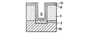
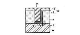
- ⁇ Plasma TiN film formation (thin film formation process)> After the Ti film 8 is formed as described above, a thin film forming process for forming a thin film made of a TiN film (titanium nitride film) using plasma is performed (S2). This thin film forming process is continuously performed in the same processing vessel 22 following the above process.
- a thin film made of the film 10 is formed by a plasma CVD method.
- the semiconductor wafer W is heated and maintained at a predetermined temperature by the heating means 38 including a resistance heater.
- the TiN film 10 is deposited not only on the top surface of the semiconductor wafer W but also on the bottom surface and side surfaces in the recess 6.
- the TiN film 10 is formed by the plasma CVD method having a higher directivity of film formation than the normal thermal CVD method, it is compared with the case of film formation by the conventional thermal CVD method.
- a very thin TiN film 10 is formed on the side surface of the recess 6, which is difficult to deposit.
- the applied high frequency power is, for example, in the range of 400 to 1000 W (watts).
- the process time is set so that the thickness of the TiN film 10 deposited on the bottom of the recess 6 falls within a range of 2 to 10 nm, for example.
- the nitriding of the TiN film 10 is appropriately performed, and the film quality is improved and stabilized.
- the barrier property is improved and the specific resistance is also reduced.
- the process pressure is in the range of 400 to 667 Pa as described later, and the process temperature is in the range of 400 to 700 ° C., for example.
- the flow rate of each gas is Ar gas in the range of 500 to 2000 sccm, H 2 gas in the range of 500 to 5000 sccm, and NH 3 gas in the range of 100 to 2000 sccm, for example.
- the partial pressure of NH 3 gas is in the range of 44 to 308 Pa, for example.
- the applied high frequency power is, for example, in the range of 400 to 1000 W (watts).
- the process time of this nitriding treatment is in the range of 5 to 60 sec, preferably in the range of 10 to 40 sec, more preferably in the range of 15 to 30 sec, as will be described later. If this process time is shorter than 5 seconds, the effect of the nitriding treatment is insufficient, and not only the barrier property becomes insufficient but also the specific resistance becomes high, which is not preferable. On the other hand, when the process time is longer than 60 sec, nitriding is excessively performed, which is not preferable because not only the barrier property is insufficient but also the specific resistance is increased.
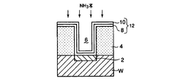
- the film quality characteristics composed of the Ti film 8 and the plasma nitriding TiN film 10 are suitable as a good barrier layer 12.
- the recess 6 is filled with the conductive film 9.
- a tungsten film is embedded as the conductive material by a thermal CVD process, or copper is embedded as the conductive material by a plating process.
- this conductive material is not limited to tungsten or copper.
- the unnecessary conductive film 9 on the upper surface of the semiconductor wafer W is scraped off and removed.
- the removal method for example, an etching process or CMP (Chemical Mechanical Polishing) or the like is used.
- the Ti film 8 is formed in the lower layer of the TiN film 10, but an embodiment in which only the TiN film 10 is formed without forming the Ti film 8 may be employed.
- the barrier layer 12 has a single layer structure consisting of only the TiN film 10.
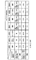
- FIG. 4 is a table illustrating the evaluation of barrier properties between a TiN film that has not been subjected to plasma nitriding and a TiN film that has been subjected to plasma nitriding.
- FIG. 5 is a table for explaining the evaluation of barrier properties when a plasmaless annealing process is performed on a TiN film formed by a thermal CVD method or an SFD method, which is a conventional film forming method.
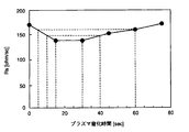
- FIG. 6 is a graph showing the relationship between the plasma nitriding time and the increasing point rate of the sheet resistance (Rs) before and after the plasma nitriding treatment.
- the barrier property in the evaluation is approximately the same as the barrier property of the two-layered barrier layer composed of the Ti film and the TiN film. It can be said.
- a TiN film was formed on a silicon substrate by a plasma CVD method to form a barrier layer, and a Cu film was formed without plasma nitriding treatment.
- a plasma CVD method to form a barrier layer
- a Cu film was formed without plasma nitriding treatment.
- three samples of Comparative Examples 1 to 3 were prepared by changing the flow rate of the TiCl 4 gas as the source gas or changing the process pressure. These samples were annealed for 30 minutes in an Ar atmosphere at 400 ° C. and 10 Torr (1333 Pa).
- the method of evaluation is the same as in Examples 1 to 4. That is, the barrier property was evaluated by measuring the sheet resistance before and after the annealing treatment.
- the thickness of the TiN film was all set to 10 nm except for Example 4.
- Example 1 Same as Example 3 During film formation: Example 1 except that the process pressure was lowered to 400 Pa Same as in plasma nitriding: same as Example 1 [Example 4] During film formation: Same as Example 1 except that the film thickness was set to 2 nm. Plasma nitridation: Same as Example 1
- Process conditions of Comparative Examples 1 to 3 that is, process temperature, process pressure, gas flow rate, applied high frequency power, and film thickness are as follows (see FIG. 4).
- FIG. 4 shows the Rs increase point rate after 30 min annealing and its evaluation in Comparative Examples 1 to 3 and Examples 1 to 4.
- “x” indicates NG (defective), and “ ⁇ ” indicates good.
- the Rs increase point rates of Comparative Examples 1 to 3 were 15.7%, 94.2%, and 32.2%, respectively, and the barrier properties of the TiN film were not so good.
- they are 3.3%, 8.3%, 4.1%, and 0.0%, which are all lower than the standard value of 10%, and the barrier property is greatly increased. It was found that it was improved.
- Each Rs increase point rate (excluding Comparative Example 2) is also represented as a graph in FIG. From the above, it can be seen that in order to improve the barrier property of the TiN film, it is necessary to perform plasma nitriding after the formation of the TiN film by plasma. Further, according to FIG. 6, it can be recognized that the longer the plasma nitriding treatment, the lower the Rs increase point rate and the higher the barrier property. As will be described later, this Rs increase point rate is It is considered that the time is about 30 seconds and the bottom starts and then rises.
- the barrier property can be improved by subjecting the TiN film to plasma nitriding.
- the improvement of the barrier property by the method of the present invention is effective when the thickness of the TiN film is 2 to 10 nm. In other words, it has been found that sufficient barrier properties can be obtained even if the barrier layer is thinned to 2 nm.
- a plasma is not used to form a TiN film on a silicon substrate, a TiN film is formed by a thermal CVD method or SFD method as a barrier layer, and plasma is not used for this.
- the sample was subjected to NH 3 nitridation treatment according to, and a Cu film was further formed on the TiN film by sputtering.
- four samples of Comparative Examples 4 to 7 were made by changing the process temperature and film thickness. These samples were annealed for 30 minutes in an Ar atmosphere at 400 ° C. and 10 Torr (1333 Pa). Then, the sheet resistance before and after the annealing treatment was measured as in the previous evaluation experiment, and the barrier property was evaluated. The result at this time is shown in FIG.
- the SFD film formation is a film formation method in which deposition (deposition) and nitridation are alternately repeated while flowing each gas flow rate, and a thin film is laminated over a plurality of layers. And one cycle.
- the plasma nitriding time in the nitriding step is preferably in the range of 5 to 60 seconds. If this time is shorter than 5 sec, not only the Rs value is large, but also the barrier property cannot be sufficiently exhibited. On the other hand, if this time is longer than 60 sec, the Rs value becomes excessively large, which is not preferable. In this case, as shown below, the graph shown in FIG. 6 is also expected to draw a downward characteristic curve, that is, it is presumed that the barrier property is also deteriorated.
- a more preferable range of the plasma nitriding time is in the range of 10 to 40 sec.
- a more preferable range is within the range of 15 to 30 sec which is the bottom portion of the curve.
- Ar gas is used as the plasma gas, but the present invention is not limited to this.
- Other noble gases such as He and Ne may be used.
- NH 3 gas is used as the nitriding gas in the plasma nitriding step, the present invention is not limited to this.
- N 2 gas, hydrazine (H 2 N—NH 2 ) gas, monomethyl hydrazine (CH 3 —NH—NH 2 ) gas, or the like may be used.
- TiCl 4 gas is used as the source gas, but the present invention is not limited to this.
- TDMAT (Ti [N (CH 3 ) 2 ] 4 : tetrakisdimethylaminotitanium) gas, TDEAT (Ti [N (C 2 H 5 ) 2 ] 4 : tetrakisdiethylaminotitanium) gas, or the like may be used.
- a semiconductor wafer has been described as an example of the object to be processed, but the semiconductor wafer includes a silicon substrate or a compound semiconductor substrate such as GaAs, SiC, GaN. Furthermore, the present invention is not limited to these substrates, and the present invention can also be applied to glass substrates, ceramic substrates, and the like used in liquid crystal display devices.
Landscapes
- Chemical & Material Sciences (AREA)
- General Chemical & Material Sciences (AREA)
- Chemical Kinetics & Catalysis (AREA)
- Engineering & Computer Science (AREA)
- Materials Engineering (AREA)
- Mechanical Engineering (AREA)
- Metallurgy (AREA)
- Organic Chemistry (AREA)
- Inorganic Chemistry (AREA)
- Chemical Vapour Deposition (AREA)
- Internal Circuitry In Semiconductor Integrated Circuit Devices (AREA)
- Electrodes Of Semiconductors (AREA)
Abstract
Description
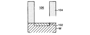
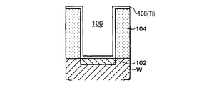
前記Ti膜108は、例えばスパッタ成膜処理やTiCl4 を用いたプラズマCVD(Chemical Vapor Deposition)法によって形成され、前記TiN膜110は、例えばTiCl4 ガス等を用いた熱CVD法や原料ガスと窒化ガスとを交互に流すSFD(Sequential Flow Deposition)法によって形成される。前記のようにしてバリヤ層112が形成されたならば、凹部106内がタングステン等の導電材料で埋め込められ、その後、余分な導電材料がエッチング等によって削り取られる。
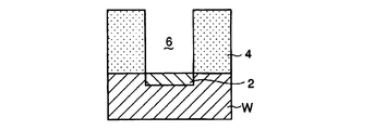
次に、以上のように構成されたプラズマ処理装置を用いて行われる本発明の成膜方法の一実施形態について、図1乃至図3を参照して説明する。ここでは、プラズマ処理方法の一例として、Ti膜及びTiN膜を成膜し、その後に窒化処理する場合を説明する。
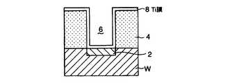
前述のように、半導体ウエハWを搬入した後に処理容器22内を密閉したならば、Ti膜の成膜が行われる(図3のS1)。まず、ガス供給手段50から、原料ガスのTiCl4 ガスと、還元ガスのH2 ガスと、プラズマ用ガスのArガスとが、それぞれガス導入手段であるシャワーヘッド40に所定の流量で流されると共に、これらの各ガスがシャワーヘッド40から処理容器22内に導入され、且つ、真空排気系28の真空ポンプ32により処理容器22内が真空引きされて、所定の圧力が維持される。
以上のようにしてTi膜8の成膜処理が行われたならば、次に、プラズマを用いてTiN膜(窒化チタン膜)よりなる薄膜を形成する薄膜成膜工程が行われる(S2)。この薄膜成膜工程は、同じ処理容器22内で、前記工程に続いて連続的に行われる。
以上のようにしてTiN膜10の成膜処理が行われたならば、次に、本発明の特徴であるプラズマを用いた窒化工程が行われる(S3)。この窒化工程は、同じ処理容器22内で、前記前工程に続いて連続的に行われる。
以上のようにしてTiN膜の窒化工程が行われたならば、次に、半導体ウエハWが処理容器22内から搬出されて、埋め込み工程が行われる(S4)。この埋め込み工程では、例えば他の成膜装置によって、前記凹部6内を含む半導体ウエハWの表面に導電性材料の成膜が行われる。これにより、図2Eに示すように、前記凹部6内に前記導電性材料が埋め込まれる(埋め込み工程)。
次に、前記実施形態に従ってプラズマ窒化処理されたTiN膜の評価が行われた。その評価結果について説明する。
成膜時 :550℃、667Pa、
TiCl4/Ar/H2/N2
=12/1600/4000/200sccm、
800W、10nm(標準)
プラズマ窒化時:550℃、667Pa、
Ar/H2/NH3
=1600/2000/1500sccm
800W、30sec
[実施例2]
成膜時 :実施例1と同じ
プラズマ窒化時:プロセス時間を15secに短くした以外は実施例1
と同じ
[実施例3]
成膜時 :プロセス圧力を400Paに低くした以外は実施例1
と同じ
プラズマ窒化時:実施例1と同じ
[実施例4]
成膜時 :膜厚を2nmに薄く設定した以外は実施例1と同じ
プラズマ窒化時:実施例1と同じ
成膜時 :550℃、667Pa、
TiCl4/Ar/H2/N2
=12/1600/4000/200sccm、
800W、10nm(標準)
[比較例2]
成膜時 :TiCl4を20sccmに増加した以外は比較例1
と同じ
[比較例3]
成膜時 :プロセス圧力を400Paに低くした以外は比較例1
と同じ
成膜時 :650℃、667Pa、
TiCl4/NH3/N2=60/60/100sccm、
10nm
(成膜後の窒化 :650℃、667Pa、
NH3/N2=2000/500sccm、
25sec
[比較例5]
成膜時 :プロセス温度を550℃に低下させた以外は比較例4
と同じ
成膜後の窒化 :プロセス温度を550℃に低下させた以外は比較例4
と同じ
[比較例6](SFD成膜)
成膜時 :550℃、260Pa、
TiCl4/NH3/N2=60/60/340sccm、
窒化時 :550℃、260Pa、
NH3/N2=4500/400sccm、
10サイクル、膜厚は10nm
[比較例7](SFD成膜)
成膜時 :比較例6と同じ、
窒化時 :2サイクル、膜厚は2nmである以外は比較例6と同じ
ところで、前述したように、バリヤ性が良好であっても、プラズマ窒化処理の結果、比抵抗が過度に増加してしまえば、バリヤ層として採用することはできない。そこで、プラズマ窒化時間に対するRs値の依存性について実験を行った。その評価結果について説明する。
Claims (14)
- 凹部を有する絶縁層が表面に形成された被処理体に対して薄膜を形成する成膜方法において、
前記凹部内の表面を含む前記被処理体の表面に、プラズマCVD法を用いて、窒化チタン膜の薄膜を形成する薄膜形成工程と、
窒化ガスの存在下で、プラズマを用いた窒化処理を行うことにより、前記薄膜を窒化する窒化工程と、
を備えたことを特徴とする成膜方法。 - 前記薄膜形成工程では、原料ガスとして、TiCl4 ガスが用いられる
ことを特徴とする請求項1に記載の成膜方法。 - 前記薄膜形成工程において、前期凹部内の底部に形成される前記薄膜の厚さは、2~10nmの範囲内である
ことを特徴とする請求項1または2に記載の成膜方法。 - 前記窒化工程におけるプロセス時間は、5~60secの範囲内である
ことを特徴とする請求項1乃至3のいずれかに記載の成膜方法。 - 前記薄膜形成工程におけるプロセス圧力は、400~667Paの範囲内である
ことを特徴とする請求項1乃至4のいずれかに記載の成膜方法。 - 前記窒化工程で用いられる前記窒化ガスは、NH3 ガスである
ことを特徴とする請求項1乃至5のいずれかに記載の成膜方法。 - 前記薄膜形成工程の前工程として、前記凹部内の表面を含む前記被処理体に、プラズマCVD法を用いて、チタン膜よりなる薄膜を形成するチタン膜形成工程が行われる
ことを特徴とする請求項1乃至6のいずれかに記載の成膜方法。 - 前記チタン膜形成工程と前記薄膜形成工程と前記窒化工程とは、同一の処理容器内で連続的に行われる
ことを特徴とする請求項7に記載の成膜方法。 - 前記チタン膜形成工程の後であって前記薄膜形成工程の前に、前記チタン膜よりなる薄膜を窒化ガスの存在下でプラズマを用いて窒化するチタン膜窒化工程が行われる
ことを特徴とする請求項7に記載の成膜方法。 - 前記チタン膜形成工程と前記チタン膜窒化工程と前記薄膜形成工程と前記窒化工程とは、同一の処理容器内で連続的に行われる
ことを特徴とする請求項9に記載の成膜方法。 - 前記窒化工程の後に、前記凹部内を導電性材料で埋め込む埋め込み工程が行なわれる
ことを特徴とする請求項1乃至10のいずれかに記載の成膜方法。 - 前記凹部の内径又は幅は、50nm以下に設定されている
ことを特徴とする請求項1乃至11のいずれかに記載の成膜方法。 - 凹部を有する絶縁層が表面に形成された被処理体に対して薄膜を形成するプラズマ処理装置において、
真空排気が可能になされた処理容器と、
前記処理容器内に配置され、前記被処理体を載置すると共に下部電極として機能する載置台と、
前記被処理体を加熱する加熱手段と、
前記処理容器内に配置され、当該処理容器内へ所定のガスを導入すると共に上部電極として機能するガス導入手段と、
前記ガス導入手段へ前記所定のガスを供給するガス供給手段と、
前記載置台と前記ガス導入手段との間にプラズマを形成するプラズマ形成手段と、
請求項1乃至12のいずれかに記載の成膜方法を実施するように前記各手段を制御する制御部と、
を備えたことを特徴とするプラズマ処理装置。 - 凹部を有する絶縁層が表面に形成された被処理体に対して薄膜を形成するプラズマ処理装置であって、
真空排気が可能になされた処理容器と、
前記処理容器内に配置され、前記被処理体を載置すると共に下部電極として機能する載置台と、
前記被処理体を加熱する加熱手段と、
前記処理容器内に配置され、当該処理容器内へ所定のガスを導入すると共に上部電極として機能するガス導入手段と、
前記ガス導入手段へ前記所定のガスを供給するガス供給手段と、
前記載置台と前記ガス導入手段との間にプラズマを形成するプラズマ形成手段と、
を備えたプラズマ処理装置を制御して、請求項1乃至12のいずれかに記載の成膜方法を実施する
コンピュータ読み取り可能なプログラム
を記憶することを特徴とする記憶媒体。
Priority Applications (1)
| Application Number | Priority Date | Filing Date | Title |
|---|---|---|---|
| CN2010800059397A CN102301454A (zh) | 2009-01-28 | 2010-01-27 | 成膜方法和等离子体成膜装置 |
Applications Claiming Priority (2)
| Application Number | Priority Date | Filing Date | Title |
|---|---|---|---|
| JP2009-017320 | 2009-01-28 | ||
| JP2009017320A JP2010177382A (ja) | 2009-01-28 | 2009-01-28 | 成膜方法及びプラズマ成膜装置 |
Publications (1)
| Publication Number | Publication Date |
|---|---|
| WO2010087362A1 true WO2010087362A1 (ja) | 2010-08-05 |
Family
ID=42395621
Family Applications (1)
| Application Number | Title | Priority Date | Filing Date |
|---|---|---|---|
| PCT/JP2010/051025 Ceased WO2010087362A1 (ja) | 2009-01-28 | 2010-01-27 | 成膜方法及びプラズマ成膜装置 |
Country Status (4)
| Country | Link |
|---|---|
| JP (1) | JP2010177382A (ja) |
| KR (1) | KR20110110261A (ja) |
| CN (1) | CN102301454A (ja) |
| WO (1) | WO2010087362A1 (ja) |
Cited By (4)
| Publication number | Priority date | Publication date | Assignee | Title |
|---|---|---|---|---|
| CN105097646A (zh) * | 2014-04-22 | 2015-11-25 | 中芯国际集成电路制造(上海)有限公司 | 一种半导体器件的制造方法 |
| CN107644813A (zh) * | 2017-09-14 | 2018-01-30 | 中国电子科技集团公司第十三研究所 | 氮化镓外延片的钝化方法 |
| CN108807385A (zh) * | 2017-04-28 | 2018-11-13 | 三星电子株式会社 | 用于制造半导体器件的方法 |
| CN112391607A (zh) * | 2019-08-19 | 2021-02-23 | 东京毅力科创株式会社 | 成膜方法和成膜装置 |
Families Citing this family (6)
| Publication number | Priority date | Publication date | Assignee | Title |
|---|---|---|---|---|
| JP2012174988A (ja) * | 2011-02-23 | 2012-09-10 | Sony Corp | 接合電極、接合電極の製造方法、半導体装置、及び、半導体装置の製造方法 |
| JP5808623B2 (ja) * | 2011-09-07 | 2015-11-10 | 株式会社アルバック | バリアメタル層の形成方法 |
| CN104213097A (zh) * | 2014-09-16 | 2014-12-17 | 朱忠良 | 铝合金的表面合金化工艺 |
| CN110875181A (zh) * | 2018-08-30 | 2020-03-10 | 长鑫存储技术有限公司 | 介电材料层及其形成方法、应用其的半导体结构 |
| KR20220167017A (ko) * | 2021-06-11 | 2022-12-20 | 주성엔지니어링(주) | 배리어층의 형성 방법 |
| CN114927525A (zh) * | 2022-04-12 | 2022-08-19 | 中国科学院微电子研究所 | 一种铁电存储器及其制备方法、应用 |
Citations (4)
| Publication number | Priority date | Publication date | Assignee | Title |
|---|---|---|---|---|
| JPH08246152A (ja) * | 1994-11-14 | 1996-09-24 | Applied Materials Inc | 化学気相堆積により堆積された改良窒化チタン層および製造法 |
| JP2001507514A (ja) * | 1995-06-05 | 2001-06-05 | マテリアルズ リサーチ コーポレーション | 窒化チタンのプラズマエンハンスアニール処理 |
| JP2001508497A (ja) * | 1997-01-31 | 2001-06-26 | 東京エレクトロン株式会社 | バイアレベル用途に用いるための、チタン上にTiN膜を低温プラズマ増速化学蒸着する方法 |
| JP2001319894A (ja) * | 2000-01-26 | 2001-11-16 | Applied Materials Inc | 金属窒化物層のプラズマcvd |
-
2009
- 2009-01-28 JP JP2009017320A patent/JP2010177382A/ja active Pending
-
2010
- 2010-01-27 CN CN2010800059397A patent/CN102301454A/zh active Pending
- 2010-01-27 WO PCT/JP2010/051025 patent/WO2010087362A1/ja not_active Ceased
- 2010-01-27 KR KR1020117017698A patent/KR20110110261A/ko not_active Abandoned
Patent Citations (4)
| Publication number | Priority date | Publication date | Assignee | Title |
|---|---|---|---|---|
| JPH08246152A (ja) * | 1994-11-14 | 1996-09-24 | Applied Materials Inc | 化学気相堆積により堆積された改良窒化チタン層および製造法 |
| JP2001507514A (ja) * | 1995-06-05 | 2001-06-05 | マテリアルズ リサーチ コーポレーション | 窒化チタンのプラズマエンハンスアニール処理 |
| JP2001508497A (ja) * | 1997-01-31 | 2001-06-26 | 東京エレクトロン株式会社 | バイアレベル用途に用いるための、チタン上にTiN膜を低温プラズマ増速化学蒸着する方法 |
| JP2001319894A (ja) * | 2000-01-26 | 2001-11-16 | Applied Materials Inc | 金属窒化物層のプラズマcvd |
Cited By (5)
| Publication number | Priority date | Publication date | Assignee | Title |
|---|---|---|---|---|
| CN105097646A (zh) * | 2014-04-22 | 2015-11-25 | 中芯国际集成电路制造(上海)有限公司 | 一种半导体器件的制造方法 |
| CN108807385A (zh) * | 2017-04-28 | 2018-11-13 | 三星电子株式会社 | 用于制造半导体器件的方法 |
| CN108807385B (zh) * | 2017-04-28 | 2024-04-30 | 三星电子株式会社 | 用于制造半导体器件的方法 |
| CN107644813A (zh) * | 2017-09-14 | 2018-01-30 | 中国电子科技集团公司第十三研究所 | 氮化镓外延片的钝化方法 |
| CN112391607A (zh) * | 2019-08-19 | 2021-02-23 | 东京毅力科创株式会社 | 成膜方法和成膜装置 |
Also Published As
| Publication number | Publication date |
|---|---|
| CN102301454A (zh) | 2011-12-28 |
| KR20110110261A (ko) | 2011-10-06 |
| JP2010177382A (ja) | 2010-08-12 |
Similar Documents
| Publication | Publication Date | Title |
|---|---|---|
| WO2010087362A1 (ja) | 成膜方法及びプラズマ成膜装置 | |
| US10026616B2 (en) | Method of reducing stress in metal film and metal film forming method | |
| JP6416679B2 (ja) | タングステン膜の成膜方法 | |
| JP6437324B2 (ja) | タングステン膜の成膜方法および半導体装置の製造方法 | |
| JP6706903B2 (ja) | タングステン膜の成膜方法 | |
| JP6391355B2 (ja) | タングステン膜の成膜方法 | |
| WO2015080058A1 (ja) | タングステン膜の成膜方法 | |
| JP3381774B2 (ja) | CVD−Ti膜の成膜方法 | |
| JP5599623B2 (ja) | 堆積チャンバにおける酸化からの導電体の保護 | |
| JP5560589B2 (ja) | 成膜方法及びプラズマ成膜装置 | |
| WO2010001931A1 (ja) | 薄膜の成膜方法及び成膜装置 | |
| JP5526189B2 (ja) | Cu膜の形成方法 | |
| JP4889227B2 (ja) | 基板処理方法および成膜方法 | |
| JP2010180434A (ja) | 成膜方法及びプラズマ成膜装置 | |
| JP6584326B2 (ja) | Cu配線の製造方法 | |
| JP2010192467A (ja) | 被処理体の成膜方法及び処理システム | |
| KR101393898B1 (ko) | 니켈막의 성막 방법 | |
| JP2011100962A (ja) | 成膜方法及びプラズマ処理装置 | |
| JP3951976B2 (ja) | プラズマ処理方法 | |
| WO2006126440A1 (ja) | 成膜方法およびコンピュータにより読み取り可能な記憶媒体 | |
| CN101484609A (zh) | 成膜方法和成膜装置 | |
| JP6608026B2 (ja) | タングステン膜の成膜方法および成膜装置 | |
| JP4650440B2 (ja) | 成膜方法 | |
| JP4157508B2 (ja) | Cvd成膜方法 | |
| JP2024047686A (ja) | 成膜方法、成膜装置、および成膜システム |
Legal Events
| Date | Code | Title | Description |
|---|---|---|---|
| WWE | Wipo information: entry into national phase |
Ref document number: 201080005939.7 Country of ref document: CN |
|
| 121 | Ep: the epo has been informed by wipo that ep was designated in this application |
Ref document number: 10735828 Country of ref document: EP Kind code of ref document: A1 |
|
| ENP | Entry into the national phase |
Ref document number: 20117017698 Country of ref document: KR Kind code of ref document: A |
|
| NENP | Non-entry into the national phase |
Ref country code: DE |
|
| 122 | Ep: pct application non-entry in european phase |
Ref document number: 10735828 Country of ref document: EP Kind code of ref document: A1 |