WO2010073824A1 - 表示パネル用の基板、及びそれを備えた表示パネル - Google Patents
表示パネル用の基板、及びそれを備えた表示パネル Download PDFInfo
- Publication number
- WO2010073824A1 WO2010073824A1 PCT/JP2009/068927 JP2009068927W WO2010073824A1 WO 2010073824 A1 WO2010073824 A1 WO 2010073824A1 JP 2009068927 W JP2009068927 W JP 2009068927W WO 2010073824 A1 WO2010073824 A1 WO 2010073824A1
- Authority
- WO
- WIPO (PCT)
- Prior art keywords
- layer
- wiring
- copper
- display panel
- substrate
- Prior art date
- Legal status (The legal status is an assumption and is not a legal conclusion. Google has not performed a legal analysis and makes no representation as to the accuracy of the status listed.)
- Ceased
Links
Images








Classifications
-
- G—PHYSICS
- G02—OPTICS
- G02F—OPTICAL DEVICES OR ARRANGEMENTS FOR THE CONTROL OF LIGHT BY MODIFICATION OF THE OPTICAL PROPERTIES OF THE MEDIA OF THE ELEMENTS INVOLVED THEREIN; NON-LINEAR OPTICS; FREQUENCY-CHANGING OF LIGHT; OPTICAL LOGIC ELEMENTS; OPTICAL ANALOGUE/DIGITAL CONVERTERS
- G02F1/00—Devices or arrangements for the control of the intensity, colour, phase, polarisation or direction of light arriving from an independent light source, e.g. switching, gating or modulating; Non-linear optics
- G02F1/01—Devices or arrangements for the control of the intensity, colour, phase, polarisation or direction of light arriving from an independent light source, e.g. switching, gating or modulating; Non-linear optics for the control of the intensity, phase, polarisation or colour
- G02F1/13—Devices or arrangements for the control of the intensity, colour, phase, polarisation or direction of light arriving from an independent light source, e.g. switching, gating or modulating; Non-linear optics for the control of the intensity, phase, polarisation or colour based on liquid crystals, e.g. single liquid crystal display cells
- G02F1/133—Constructional arrangements; Operation of liquid crystal cells; Circuit arrangements
- G02F1/1333—Constructional arrangements; Manufacturing methods
- G02F1/1335—Structural association of cells with optical devices, e.g. polarisers or reflectors
- G02F1/133502—Antiglare, refractive index matching layers
-
- H—ELECTRICITY
- H10—SEMICONDUCTOR DEVICES; ELECTRIC SOLID-STATE DEVICES NOT OTHERWISE PROVIDED FOR
- H10K—ORGANIC ELECTRIC SOLID-STATE DEVICES
- H10K50/00—Organic light-emitting devices
- H10K50/80—Constructional details
- H10K50/86—Arrangements for improving contrast, e.g. preventing reflection of ambient light
-
- H—ELECTRICITY
- H10—SEMICONDUCTOR DEVICES; ELECTRIC SOLID-STATE DEVICES NOT OTHERWISE PROVIDED FOR
- H10K—ORGANIC ELECTRIC SOLID-STATE DEVICES
- H10K59/00—Integrated devices, or assemblies of multiple devices, comprising at least one organic light-emitting element covered by group H10K50/00
- H10K59/10—OLED displays
- H10K59/12—Active-matrix OLED [AMOLED] displays
- H10K59/131—Interconnections, e.g. wiring lines or terminals
-
- G—PHYSICS
- G02—OPTICS
- G02F—OPTICAL DEVICES OR ARRANGEMENTS FOR THE CONTROL OF LIGHT BY MODIFICATION OF THE OPTICAL PROPERTIES OF THE MEDIA OF THE ELEMENTS INVOLVED THEREIN; NON-LINEAR OPTICS; FREQUENCY-CHANGING OF LIGHT; OPTICAL LOGIC ELEMENTS; OPTICAL ANALOGUE/DIGITAL CONVERTERS
- G02F1/00—Devices or arrangements for the control of the intensity, colour, phase, polarisation or direction of light arriving from an independent light source, e.g. switching, gating or modulating; Non-linear optics
- G02F1/01—Devices or arrangements for the control of the intensity, colour, phase, polarisation or direction of light arriving from an independent light source, e.g. switching, gating or modulating; Non-linear optics for the control of the intensity, phase, polarisation or colour
- G02F1/13—Devices or arrangements for the control of the intensity, colour, phase, polarisation or direction of light arriving from an independent light source, e.g. switching, gating or modulating; Non-linear optics for the control of the intensity, phase, polarisation or colour based on liquid crystals, e.g. single liquid crystal display cells
- G02F1/133—Constructional arrangements; Operation of liquid crystal cells; Circuit arrangements
- G02F1/136—Liquid crystal cells structurally associated with a semi-conducting layer or substrate, e.g. cells forming part of an integrated circuit
- G02F1/1362—Active matrix addressed cells
- G02F1/136286—Wiring, e.g. gate line, drain line
- G02F1/13629—Multilayer wirings
-
- G—PHYSICS
- G02—OPTICS
- G02F—OPTICAL DEVICES OR ARRANGEMENTS FOR THE CONTROL OF LIGHT BY MODIFICATION OF THE OPTICAL PROPERTIES OF THE MEDIA OF THE ELEMENTS INVOLVED THEREIN; NON-LINEAR OPTICS; FREQUENCY-CHANGING OF LIGHT; OPTICAL LOGIC ELEMENTS; OPTICAL ANALOGUE/DIGITAL CONVERTERS
- G02F1/00—Devices or arrangements for the control of the intensity, colour, phase, polarisation or direction of light arriving from an independent light source, e.g. switching, gating or modulating; Non-linear optics
- G02F1/01—Devices or arrangements for the control of the intensity, colour, phase, polarisation or direction of light arriving from an independent light source, e.g. switching, gating or modulating; Non-linear optics for the control of the intensity, phase, polarisation or colour
- G02F1/13—Devices or arrangements for the control of the intensity, colour, phase, polarisation or direction of light arriving from an independent light source, e.g. switching, gating or modulating; Non-linear optics for the control of the intensity, phase, polarisation or colour based on liquid crystals, e.g. single liquid crystal display cells
- G02F1/133—Constructional arrangements; Operation of liquid crystal cells; Circuit arrangements
- G02F1/136—Liquid crystal cells structurally associated with a semi-conducting layer or substrate, e.g. cells forming part of an integrated circuit
- G02F1/1362—Active matrix addressed cells
- G02F1/136286—Wiring, e.g. gate line, drain line
- G02F1/136295—Materials; Compositions; Manufacture processes
-
- G—PHYSICS
- G02—OPTICS
- G02F—OPTICAL DEVICES OR ARRANGEMENTS FOR THE CONTROL OF LIGHT BY MODIFICATION OF THE OPTICAL PROPERTIES OF THE MEDIA OF THE ELEMENTS INVOLVED THEREIN; NON-LINEAR OPTICS; FREQUENCY-CHANGING OF LIGHT; OPTICAL LOGIC ELEMENTS; OPTICAL ANALOGUE/DIGITAL CONVERTERS
- G02F2202/00—Materials and properties
-
- G—PHYSICS
- G02—OPTICS
- G02F—OPTICAL DEVICES OR ARRANGEMENTS FOR THE CONTROL OF LIGHT BY MODIFICATION OF THE OPTICAL PROPERTIES OF THE MEDIA OF THE ELEMENTS INVOLVED THEREIN; NON-LINEAR OPTICS; FREQUENCY-CHANGING OF LIGHT; OPTICAL LOGIC ELEMENTS; OPTICAL ANALOGUE/DIGITAL CONVERTERS
- G02F2203/00—Function characteristic
- G02F2203/01—Function characteristic transmissive
-
- H—ELECTRICITY
- H10—SEMICONDUCTOR DEVICES; ELECTRIC SOLID-STATE DEVICES NOT OTHERWISE PROVIDED FOR
- H10K—ORGANIC ELECTRIC SOLID-STATE DEVICES
- H10K59/00—Integrated devices, or assemblies of multiple devices, comprising at least one organic light-emitting element covered by group H10K50/00
- H10K59/80—Constructional details
- H10K59/8791—Arrangements for improving contrast, e.g. preventing reflection of ambient light
Definitions
- the present invention relates to a display panel substrate and a display panel including the substrate.
- display panels using liquid crystal, organic EL, inorganic EL, and the like have been rapidly spread.
- an active matrix substrate having a high response speed and easy multi-gradation display is provided. Display panels are widely used.
- a display panel including an active matrix substrate includes an active matrix substrate in which a large number of pixels are arranged in a matrix, and a counter substrate disposed so as to face the active matrix substrate, and further between the two substrates.
- a liquid crystal layer, an organic EL layer, or the like, which is a display medium is sandwiched.
- a plurality of gate wirings and a plurality of source wirings are arranged to intersect with each other, and a pixel portion having a TFT is formed in the vicinity of the intersection.
- Patent Document 1 discloses an etching solution that can be used for forming a wiring having a two-layer structure of copper and titanium or a three-layer structure of titanium / copper / titanium.
- Patent Document 2 discloses an etching solution for collectively etching a wiring that is a double metal layer and whose upper layer is made of copper.
- Patent Document 3 describes an array substrate for a liquid crystal display device having a double metal layer and an upper layer made of copper.
- the above-mentioned conventional active matrix substrate has a problem that when used in a display panel, external light is reflected by a metal having high reflectivity in the wiring, leading to a decrease in contrast in a bright room.
- the present invention has been made in view of the above problems, and provides a display panel substrate capable of suppressing reflection of external light and increasing contrast in a bright room, and a display panel including the substrate. With the goal.
- the wiring provided in the display region on the substrate is composed of a plurality of layers, and the uppermost layer of the plurality of layers is It is characterized by being comprised by the oxide of the 1st metal selected from the group which consists of copper, titanium, and molybdenum, or the nitride of copper.
- the oxide of copper, titanium or molybdenum, or copper nitride has a much lower reflectivity than metal, so the reflection in the uppermost layer of the wiring provided in the display area on the substrate The rate can be lowered. Accordingly, it is possible to form a display panel in which reflection of external light is suppressed and contrast in a bright room is increased.
- a display panel according to the present invention includes the above-described substrate. Therefore, it is possible to realize a display panel in which reflection of external light is suppressed and contrast in a bright room is increased.
- the wiring provided in the display region on the substrate is composed of a plurality of layers, and the uppermost layer of the plurality of layers includes copper, titanium, and the like. Since the first metal oxide selected from the group consisting of molybdenum or copper nitride is used, reflection of external light can be suppressed and contrast in a bright room can be increased.
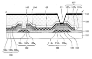
- 1 is a cross-sectional view of an active matrix substrate in an embodiment of the present invention.
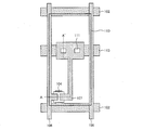
- 1 is a plan view of an active matrix substrate in the present embodiment. It is sectional drawing which shows the gate wiring 102 in this Embodiment. It is sectional drawing of the active matrix substrate in this Embodiment.
- 1 is a plan view of an active matrix substrate in the present embodiment. It is sectional drawing in the 1st metal film-forming process of the active matrix substrate in this Embodiment. It is sectional drawing in the gate wiring 102 formation process of the active matrix substrate in this Embodiment. It is sectional drawing in the gate insulating film 103 / semiconductor layer 104 film-forming process of the active matrix substrate in this Embodiment.
- liquid crystal display panel including an active matrix substrate
- the liquid crystal display panel according to the present embodiment is formed by bonding an active matrix substrate (substrate) and a counter substrate with a liquid crystal layer interposed therebetween.
- pixel electrodes (transparent electrodes) 110 are arranged in a matrix, and are provided in a display area for displaying an image that can be viewed by an observer, and outside the display area, and the image is not visually recognized by an observer. It is divided into a non-display area. 1 and 2 show one pixel electrode 110 in the display region.
- FIG. 1 shows a cross-sectional view of an active matrix substrate in the present embodiment.
- FIG. 2 is a plan view of the active matrix substrate in the present embodiment.
- FIG. 1 is a cross-sectional view taken along line A-A ′ in FIG.
- an active matrix substrate in this embodiment includes a gate wiring (wiring) 102, a source wiring (wiring) 106, a compensation capacitor electrode (wiring) 113, and a drain electrode (wiring) on a glass substrate 101. 107) are formed, and a gate insulating film 103, a semiconductor layer 104, an N + contact layer 105, a passivation film 108, and an interlayer insulating film 109 are provided between these wirings and electrodes. Further, a pixel electrode 110 is formed on the interlayer insulating film 109.
- the active matrix substrate is arranged so that the plurality of gate wirings 102 and the plurality of source wirings 106 intersect, and a pixel portion having TFTs is formed in the vicinity of the intersections. Yes.
- a drain electrode 107 and a pixel electrode 110 are provided corresponding to each TFT.
- a compensation capacitance electrode 113 for forming an auxiliary capacitance is provided between the pixel electrode 110 and the pixel electrode 110.
- a wiring includes a wiring, an electrode, and the like.
- the wiring indicates a gate wiring 102, a source wiring 106, a drain electrode 107, and a compensation capacitor electrode 113.
- the display area can also be said to be an area where external light irradiated on the display surface from the observer side reaches in the display panel. External light refers to light from indoor lamps, sunlight, and the like outside the display panel.
- the light is emitted from the pixel electrode 110 side.
- the gate wiring 102 includes a copper oxide layer (uppermost layer) 102c, a copper layer (first layer) 102b, and a titanium layer (second layer) 102a. Each of these layers will be described in detail below.
- the copper oxide layer 102c is provided on the uppermost layer of the gate wiring 102 and is a layer containing an oxide of copper (Cu) (first metal).
- the copper oxide include copper oxide (II) (CuO), copper oxide (I) (Cu 2 O), and the like.
- the copper oxide layer 102c may be formed using copper nitride, titanium (Ti), or molybdenum (Mo) oxide instead of copper oxide. That is, the first metal in the present invention is not limited to Cu, but may be Ti, Mo, or the like.
- oxides or nitrides include copper nitride (Cu 3 N), titanium dioxide (TiO 2 ), molybdenum trioxide (MoO 3 ), and molybdenum dioxide (MoO 2 ).
- the reflectance in the copper oxide layer 102c is low. Since the gate wiring 102 in this embodiment includes the copper oxide layer 102c as the uppermost layer, the reflectance on the uppermost layer side is low. Therefore, in the liquid crystal display panel, external light can be prevented from being reflected by the wiring, and the contrast in the bright room can be increased.
- the thickness of the copper oxide layer 102c is preferably 50 to 2000 mm, more preferably about 500 mm.
- the copper layer 102b is a layer containing copper.
- pure copper can be used as the copper. Since copper has low resistance, the wiring resistance can be lowered by including copper in the wiring.
- a copper alloy may be used for the copper layer 102b instead of copper.
- the copper alloy include a copper-magnesium alloy (CuMg), a copper-manganese alloy (CuMn), a copper-aluminum alloy (CuAl), a copper-titanium alloy (CuTi), a copper-zirconium alloy (CuZr), and a copper-molybdenum.
- An alloy (CuMo) or the like can be used. By using these metals, it is possible to reduce the resistance of the wiring.
- the thickness of the copper layer 102b is preferably 1000 to 10,000 mm, more preferably 1000 to 4000 mm, and still more preferably about 3000 mm. Further, it is more preferable to adjust the thickness of the copper layer 102b in order to make the wiring resistance as desired.
- the titanium layer 102a is a layer containing titanium (Ti).
- the thickness of the titanium layer 102a is preferably 50 to 500 mm, and more preferably 300 to 500 mm.
- the 2nd layer in this invention may be comprised not only with titanium but with molybdenum or molybdenum alloy.
- the molybdenum alloys include molybdenum-tungsten alloy (MoW), molybdenum-niobium alloy (MoNb), molybdenum-neodymium alloy (MoNd), molybdenum-titanium alloy (MoTi), molybdenum-tantalum alloy (MoTa), and molybdenum-nickel alloy ( MoNi), molybdenum-indium alloy (MoIn), molybdenum-aluminum alloy (MoAl), and the like.
- MoW molybdenum-tungsten alloy
- MoNb molybdenum-niobium alloy
- MoNd molybdenum-neodymium alloy
- MoTi molybdenum-titanium alloy
- MoTa molybdenum-tantalum alloy
- the gate wiring 102 preferably further has a good taper shape.
- Good taper shape refers to, for example, a shape having a smooth slope at the end.
- the bad shape is, for example, a shape in which each layer is stacked stepwise, or a shape in which the upper layer is formed with a wider width than the lower layer.
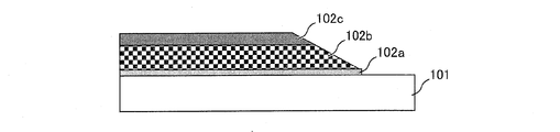
- FIG. 3 is a cross-sectional view showing the gate wiring 102 in this embodiment.
- the width of the bottom surface of the copper layer 102b is substantially the same as the width of the upper surface of the titanium layer 102a, and the width of the copper layer 102b becomes narrower as the distance from the titanium layer 102a increases. Is formed. Further, the width of the bottom surface of the copper oxide layer 102c is substantially the same as the width of the upper surface of the copper layer 102b, and is formed so as to become narrower as the distance from the copper layer 102b increases. Then, the upper part of the gate wiring 102 is formed to be narrower.
- the wiring has a good tapered shape, it is possible to prevent the copper contained in the copper layer 102b in the wiring from coming into contact with the base, that is, the glass substrate 101 or the like.
- the wiring has a good taper shape, a layer formed on the wiring, such as the copper layer 102b, can be satisfactorily covered with the gate insulating film 103 or the like in the tapered portion.
- the taper shape is poor, the copper layer 102b or the like may not be completely covered with the gate insulating film 103 or the like in the taper portion, which may cause film peeling, wiring disconnection, or the like.
- the gate wiring 102 has the above structure. Note that the source wiring 106, the drain electrode 107, and the compensation capacitor electrode 113 also have the same structure as the above-described gate wiring 102, and therefore the description of the gate wiring 102 is applied to them and the description is omitted. To do. That is, for the description of the copper oxide layer 102c, the copper layer 102b, and the titanium layer 102a in the gate wiring 102, the copper oxide layer (top layer) in the source wiring 106, the drain electrode 107, or the compensation capacitor electrode 113 (106c, 107c and 113c), copper layer (first layer) (106b, 107b and 107a) and titanium layer (second layer) (106a, 107a and 113a).
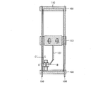
- FIG. 4 and FIG. 5 show another pixel electrode 110 in the active matrix substrate of the present embodiment.
- FIG. 4 is a cross-sectional view of the active matrix substrate in the present embodiment
- FIG. 5 is a plan view of the active matrix substrate in the present embodiment. 4 shows a cross-sectional view taken along line B-B ′ and a cross-sectional view taken along line C-C ′ in FIG. 5.
- the gate wiring 102, the source wiring 106, and the drain electrode 107 also have a three-layer structure in the other pixel electrodes 110 as described above.
- the source wiring 106 is the boundary between the two pixel electrodes 110, and only the source wiring 106 is formed as a wiring and the pixel electrode 110 is not formed. As described above, it has a three-layer structure.
- the active matrix substrate in this embodiment is formed on the uppermost layer of the gate wiring 102, the source wiring 106, the drain electrode 107, and the compensation capacitor electrode 113 provided in the display region, that is, the region where external light reaches. Since the copper oxide layer (102c, 106c, 107c, and 113c) is provided, external light is not reflected by the wiring, and a display panel with high contrast in a bright room can be manufactured.
- the wiring provided in the display region on the substrate according to the present invention only needs to be composed of a plurality of layers, and is not particularly limited to the three-layer structure as described above. It may consist of more than one layer.
- the uppermost layer of the wiring only needs to contain copper, titanium or molybdenum oxide, or copper nitride, and the layers other than the uppermost layer are not particularly limited.
- the gate insulating film 103 for example, silicon nitride (SiNx), silicon dioxide (SiO 2 ), or the like may be used, or SiNx and SiO 2 may be stacked.
- the thickness of the gate insulating film 103 is preferably 1000 to 5000 mm.
- amorphous silicon may be used for the semiconductor layer 104, and an oxide semiconductor such as an amorphous thin film (IGZO) having a composition of zinc oxide (ZnO) or indium oxide-gallium oxide-zinc oxide is used. It may be used.
- the thickness of the semiconductor layer 104 is preferably 300 to 3000 mm.
- the N + contact layer 105 may be an electrode contact layer doped with an n-type impurity at a high concentration.
- N + amorphous silicon may be used.
- the thickness of the N + contact layer 105 is preferably 500 to 1500 mm.
- silicon nitride (SiNx), silicon dioxide (SiO 2 ), or the like can be used for the passivation film 108.
- the thickness of the passivation film 108 is preferably 500 to 3000 mm.
- the interlayer insulating film 109 preferably has photosensitivity, and for example, a photosensitive acrylic resin can be used.
- the thickness of the interlayer insulating film 109 is preferably 1 to 4 ⁇ m.
- a transparent conductive material such as indium tin oxide (ITO) or indium oxide-zinc oxide (IZO) can be used.
- the thickness of the pixel electrode 110 is preferably 100 to 2000 mm.
- the drain electrode 107 and the pixel electrode 110 are electrically connected at a contact hole portion (connection portion) 111.
- a contact hole portion 111 As shown in FIG. 1, in the contact hole portion 111, a part of the copper oxide layer 107c in the drain electrode 107 is removed, and the exposed copper layer 107b and the pixel electrode 110 are in contact with each other.
- the shape of the contact hole portion 111 is not limited to a quadrangle as shown in FIG. 2 as long as the drain electrode 107 and the pixel electrode 110 are sufficiently in contact with each other, and may be, for example, a circle.
- a part of the copper oxide layer 107c to be removed may have the same shape and size as the contact hole portion 111 or may be smaller than the contact hole portion 111, but the copper layer 107b and the pixel electrode It is preferable that the size is sufficient for 110 to come into contact.
- the copper oxide layer 107c having a high connection resistance with the pixel electrode 110 is removed, and the copper layer 107b is in contact with the pixel electrode 110. Therefore, the pixel electrode 110 has a low resistance. And the drain electrode 107 can be connected.
- FIGS. 6 to 16 are cross-sectional views in each manufacturing process of the active matrix substrate in the present embodiment, and show a cross-sectional structure at the time when each process is completed.
- a process of manufacturing the structure shown in FIG. 1 will be described.
- 6 to 16 are sectional views taken along line AA ′ in FIG.
- FIG. 6 is a cross-sectional view of the active matrix substrate in the first embodiment in the first metal film forming step.
- the titanium film 1 and the copper film 2 are formed on the glass substrate 101 by a sputtering method. Thereafter, oxygen (O 2 ) is added to normal argon (Ar) as a sputtering gas, and CuO is formed as the copper oxide film 3 by a reactive sputtering method in which copper and oxygen are reacted.
- the O 2 partial pressure in the sputtering gas is preferably 1 to 30%, more preferably about 10%.
- copper (N 2 ) is added to the sputtering gas instead of oxygen.
- a reactive sputtering method in which nitrogen and nitrogen are reacted can be used.
- the N 2 partial pressure in the sputtering gas at this time is preferably 10 to 90%, more preferably about 50%.
- FIG. 7 is a cross-sectional view in the step of forming the gate wiring 102 of the active matrix substrate in the present embodiment.
- a resist pattern is formed by photolithography, a pattern of the gate wiring 102 and the compensation capacitor electrode 113 is formed by a wet etching method, and then the resist is peeled and washed.
- an etchant used in the wet etching method it is preferable to use an etchant containing hydrogen peroxide, an inorganic acid, a fluorine compound, and water.
- the inorganic acid include hydrochloric acid, sulfuric acid, nitric acid, phosphoric acid and the like.
- the fluorine compound include hydrofluoric acid, ammonium fluoride, and potassium fluoride.
- the concentration of the fluorine compound is preferably adjusted so as not to affect the underlying glass substrate 101 and the like.
- the etching solution may further contain an organic acid.
- the organic acid include carboxylic acid, amino acid, citric acid, tartaric acid, oxalic acid and the like.
- Patent Document 1 one disclosed in US Pat. No. 7,0085,848 (Patent Document 1) can be used.
- the Cu layer has the following formulas (A) and (B), and the Ti layer has the following formula: Etching is performed by the reaction of the formula (C).
- Etching is performed by the reaction of the formula (C).
- the reaction of the above formulas (A) and (B) proceeds faster than the reaction of the above formula (C).
- the fluorine compound since the fluorine compound has an influence on the glass substrate 101 as a base, the concentration cannot be increased.
- the Cu layer is etched faster than the Ti layer.
- the etching rate of the Cu layer is the etching rate of the CuO layer by the reaction of the above formula (B).
- the wiring can be formed into a good taper shape as described above. Similar effects can be obtained when a layer containing other oxides or nitrides such as Cu 2 O and copper nitride is used instead of the CuO layer.
- the gate wiring 102 and the compensation capacitor electrode 113 can be formed into a good tapered shape as described above.
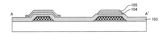
- FIG. 8 is a cross-sectional view in the step of forming the gate insulating film 103 / semiconductor layer 104 of the active matrix substrate in this embodiment.
- N + amorphous silicon is deposited as amorphous silicon, and N + contact layer 105 as a semiconductor layer 104.
- the gate insulating film 103, the semiconductor layer 104, and the N + contact layer 105 are continuously formed.
- the present invention is not limited to this, and these layers are formed separately. Also good.
- FIG. 9 is a cross-sectional view in the semiconductor layer 104 pattern forming step of the active matrix substrate in the present embodiment.
- the semiconductor layer 104 and the N + contact layer 105 are etched by, for example, a dry etching method to form a pattern. Thereafter, the resist is peeled and washed.
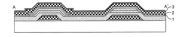
- FIG. 10 is a cross-sectional view of the active matrix substrate in the second embodiment in the second metal film forming step.
- the titanium film 1, the copper film 2, and the copper oxide film 3 are formed using the same method as the above-described (1) first metal film forming step.
- FIG. 11 is a cross-sectional view in the source wiring 106 pattern formation step of the active matrix substrate in the present embodiment.
- a resist pattern is formed by photolithography, and a pattern of the source wiring 106 and the drain electrode 107 is formed by a wet etching method.
- the wet etching method can be performed in the same manner as the above-described (2) gate wiring 102 forming step. Thereby, the source wiring 106 and the drain electrode 107 can be made into the favorable taper shape as mentioned above.
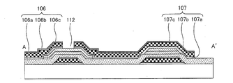
- FIG. 12 is a cross-sectional view in the step of etching the channel portion 112 of the active matrix substrate in the present embodiment.
- the N + contact layer 105 and part of the semiconductor layer 104 are removed in the channel portion 112 between the source wiring 106 and the drain electrode 107 by dry etching, and the source wiring 106 and the drain electrode 107 are removed. Isolate. Thereafter, the resist is peeled and washed.
- FIG. 13 is a cross-sectional view in the step of forming the passivation film 108 on the active matrix substrate in the present embodiment.
- silicon nitride is formed as the passivation film 108 by the CVD method.
- FIG. 14 is a cross-sectional view in the step of forming the interlayer insulating film 109 of the active matrix substrate in the present embodiment.
- a photosensitive acrylic resin is formed as the interlayer insulating film 109, and a pattern of the contact hole portion 111 is formed by photolithography.
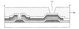
- FIG. 15 is a cross-sectional view in the etching process of the contact hole 111 of the active matrix substrate in the present embodiment.
- FIG. 16 is a cross-sectional view in the step of removing the copper oxide layer 107c from the active matrix substrate in the present embodiment.
- the copper oxide layer 107c of the drain electrode 107 in the contact hole portion 111 is removed by a wet etching method.
- a wet etching method for example, hydrochloric acid, nitric acid, or the like can be used.
- a resist pattern is formed by photolithography. Thereafter, the pattern of the pixel electrode 110 is formed by wet etching, and then the resist is peeled and washed.
- an etchant used for wet etching for example, salt iron, oxalic acid, a mixed solution of phosphoric acid, acetic acid, and nitric acid, or the like can be used.
- the pixel electrode 110 and the copper layer 107b come into contact with each other, and as a result, the pixel electrode 110 and the drain electrode 107 are connected with low resistance. be able to.
- the active matrix substrate in the present embodiment is manufactured.
- the materials as described above and the thicknesses of the respective layers are not necessarily limited, and materials conventionally used as a material for the active matrix substrate can be used.
- the display panel substrate according to the present invention is not limited to the active matrix type, and may be a passive matrix type, for example.
- the substrate according to the present invention can also be applied to a display panel using organic EL, inorganic EL, or the like.
- the display panel substrate according to the present invention preferably further includes a first layer made of copper or a copper alloy below the uppermost layer.
- the wiring further includes a second layer made of titanium below the first layer.
- the wiring preferably further includes a second layer made of molybdenum or a molybdenum alloy below the first layer.
- the etching rate of the copper or copper alloy of the first layer can be increased by etching in a batch with an etching solution containing hydrogen peroxide, an inorganic acid and a fluorine compound.
- a favorable tapered wiring can be easily formed.
- the display panel substrate according to the present invention further includes a connection portion for connecting the wiring and a transparent electrode provided on the wiring, and the connection portion includes an uppermost layer of the wiring. It is preferable that a part of the first electrode is removed and the exposed first layer is in contact with the transparent electrode.
- connection part which wiring and a transparent electrode connect the uppermost layer comprised by the 1st metal oxide or copper nitride with high connection resistance with a transparent electrode is removed. Since the first layer and the transparent electrode are in contact, the transparent electrode and the wiring can be connected with low resistance.
- the wiring is at least one selected from the group consisting of a gate wiring, a source wiring, a drain electrode, and a compensation capacitor electrode.
- the present invention it is possible to provide a display panel substrate capable of suppressing reflection of external light and increasing contrast in a bright room, and a display panel including the substrate. Therefore, when manufacturing a high-quality display device Can be suitably used.
Landscapes
- Physics & Mathematics (AREA)
- Nonlinear Science (AREA)
- Optics & Photonics (AREA)
- Mathematical Physics (AREA)
- Chemical & Material Sciences (AREA)
- Crystallography & Structural Chemistry (AREA)
- General Physics & Mathematics (AREA)
- Engineering & Computer Science (AREA)
- Microelectronics & Electronic Packaging (AREA)
- Thin Film Transistor (AREA)
- Liquid Crystal (AREA)
Abstract
Description
本実施の形態におけるアクティブマトリクス基板の構成について、図1及び図2を参照しながら以下に説明する。
銅酸化物層102cは、ゲート配線102の最上層に設けられており、銅(Cu)(第1の金属)の酸化物を含む層である。銅の酸化物としては、例えば酸化銅(II)(CuO)、酸化銅(I)(Cu2O)等が挙げられる。なお、銅酸化物層102cには、銅の酸化物に代えて、銅の窒化物、あるいは、チタン(Ti)又はモリブデン(Mo)の酸化物、などを用いてもよい。すなわち、本発明における第1の金属は、Cuに限らず、Ti、Mo等であってもよい。このような酸化物又は窒化物としては、例えば、窒化銅(Cu3N)、二酸化チタン(TiO2)、三酸化モリブデン(MoO3)、二酸化モリブデン(MoO2)などが挙げられる。
銅層102bは、銅を含む層である。銅としては、例えば純銅などを用いることができる。銅は抵抗が低いため、配線に銅を含むことにより、配線の抵抗を低くすることができる。
チタン層102aは、チタン(Ti)を含む層である。チタン層102aの厚さは、50~500Åであることが好ましく、300~500Åであることがより好ましい。
次に、本実施の形態に係るアクティブマトリクス基板の製造工程について、図6~図16を参照して工程順に(1)~(12)に説明する。図6~図16は、本実施の形態におけるアクティブマトリクス基板の各製造工程における断面図であり、各工程が終了した時点での断面構造を示す。なお、ここでは、図1に示す構造のものを製造する工程について説明する。また、図6~図16は、図2におけるA-A’線の断面図を示している。
まず、図6に示すように、第1の金属成膜工程を行う。図6は、本実施の形態におけるアクティブマトリクス基板の第1の金属成膜工程における断面図である。
次いで、図7に示すように、ゲート配線102形成工程を行う。図7は、本実施の形態におけるアクティブマトリクス基板のゲート配線102形成工程における断面図である。
Cu+H2O2→CuO+H2O・・・(A)
CuO+2HCl→CuCl2+H2O・・・(B)
Ti+4HF→TiF4+H2・・・(C)
上記式(A)及び(B)の反応は、上記式(C)の反応よりも速く進む。また、フッ素化合物は、下地となるガラス基板101に対する影響があるため、濃度を高くすることができない。したがってCu層は、Ti層よりも速くエッチングされることとなる。ここで、本実施の形態のように、例えば配線をCuO層とCu層とTi層との3層構造にすると、Cu層のエッチング速度は、上記式(B)の反応がCuO層におけるエッチング速度に寄与することとなるために抑えられ、結果として配線を、上述したような良好なテーパー形状とすることができる。CuO層に代えて、Cu2O、銅窒化物など、他の酸化物又は窒化物を含む層を用いた場合にも、同様の効果が得られる。
次いで、図8に示すように、ゲート絶縁膜103/半導体層104成膜工程を行う。図8は、本実施の形態におけるアクティブマトリクス基板のゲート絶縁膜103/半導体層104成膜工程における断面図である。
次いで、図9に示すように、半導体層104パターン形成工程を行う。図9は、本実施の形態におけるアクティブマトリクス基板の半導体層104パターン形成工程における断面図である。
次いで、図10に示すように、第2の金属成膜工程を行う。図10は、本実施の形態におけるアクティブマトリクス基板の第2の金属成膜工程における断面図である。
次いで、図11に示すように、ソース配線106パターン形成工程を行う。図11は、本実施の形態におけるアクティブマトリクス基板のソース配線106パターン形成工程における断面図である。
次いで、図12に示すように、チャネル部112エッチング工程を行う。図12は、本実施の形態におけるアクティブマトリクス基板のチャネル部112エッチング工程における断面図である。
次いで、図13に示すように、パッシベーション膜108成膜工程を行う。図13は、本実施の形態におけるアクティブマトリクス基板のパッシベーション膜108成膜工程における断面図である。
次いで、図14に示すように、層間絶縁膜109形成工程を行う。図14は、本実施の形態におけるアクティブマトリクス基板の層間絶縁膜109形成工程における断面図である。
次いで、図15に示すように、コンタクトホール部111エッチング工程を行う。図15は、本実施の形態におけるアクティブマトリクス基板のコンタクトホール部111エッチング工程における断面図である。
次いで、図16に示すように、銅酸化物層107c除去工程を行う。図16は、本実施の形態におけるアクティブマトリクス基板の銅酸化物層107c除去工程における断面図である。
次いで、画素電極110形成工程を行い、図1に示すアクティブマトリクス基板を完成させる。
102b、106b、107b、113b 銅層(第1の層)
102c、106c、107c、113c 銅酸化物層(最上層)
102 ゲート配線(配線)
103 ゲート絶縁膜
104 半導体層
105 N+コンタクト層
106 ソース配線(配線)
107 ドレイン電極(配線)
108 パッシベーション膜
109 層間絶縁膜
110 画素電極(透明電極)
111 コンタクトホール部(接続部)
113 補償容量電極(配線)
Claims (7)
- 表示パネル用の基板であって、
上記基板上の表示領域内に設けられた配線は、複数の層からなっており、
上記複数の層の最上層は、銅、チタン及びモリブデンからなる群より選択された第1の金属の酸化物、又は銅の窒化物により構成されていることを特徴とする表示パネル用の基板。 - 上記配線は、上記最上層の下に、銅又は銅合金により構成される第1の層をさらに備えていることを特徴とする請求項1に記載の表示パネル用の基板。
- 上記配線は、第1の層の下に、チタンにより構成される第2の層をさらに備えていることを特徴とする請求項2に記載の表示パネル用の基板。
- 上記配線は、第1の層の下に、モリブデン又はモリブデン合金により構成される第2の層をさらに備えていることを特徴とする請求項2に記載の表示パネル用の基板。
- 上記配線と、上記配線の上に設けられた透明電極とが接続する接続部をさらに備えており、
上記接続部において、上記配線の最上層の一部分が除去され、露出した第1の層と上記透明電極とが接触していることを特徴とする請求項2~4の何れか1項に記載の表示パネル用の基板。 - 上記配線が、ゲート配線、ソース配線、ドレイン電極及び補償容量電極からなる群より選択される少なくとも1つであることを特徴とする請求項1~5の何れか1項に記載の表示パネル用の基板。
- 請求項1~6の何れか1項に記載の表示パネル用の基板を備えていることを特徴とする表示パネル。
Priority Applications (2)
| Application Number | Priority Date | Filing Date | Title |
|---|---|---|---|
| US13/130,583 US20110227085A1 (en) | 2008-12-26 | 2009-11-05 | Substrate for use in display panel, and display panel including same |
| CN2009801481769A CN102227761A (zh) | 2008-12-26 | 2009-11-05 | 显示面板用的基板和具有它的显示面板 |
Applications Claiming Priority (2)
| Application Number | Priority Date | Filing Date | Title |
|---|---|---|---|
| JP2008-334743 | 2008-12-26 | ||
| JP2008334743 | 2008-12-26 |
Publications (1)
| Publication Number | Publication Date |
|---|---|
| WO2010073824A1 true WO2010073824A1 (ja) | 2010-07-01 |
Family
ID=42287449
Family Applications (1)
| Application Number | Title | Priority Date | Filing Date |
|---|---|---|---|
| PCT/JP2009/068927 Ceased WO2010073824A1 (ja) | 2008-12-26 | 2009-11-05 | 表示パネル用の基板、及びそれを備えた表示パネル |
Country Status (3)
| Country | Link |
|---|---|
| US (1) | US20110227085A1 (ja) |
| CN (1) | CN102227761A (ja) |
| WO (1) | WO2010073824A1 (ja) |
Cited By (3)
| Publication number | Priority date | Publication date | Assignee | Title |
|---|---|---|---|---|
| JP2016111342A (ja) * | 2014-11-27 | 2016-06-20 | 三菱瓦斯化学株式会社 | 液体組成物およびこれを用いたエッチング方法 |
| JPWO2015029286A1 (ja) * | 2013-08-27 | 2017-03-02 | 株式会社Joled | 薄膜トランジスタ基板の製造方法及び薄膜トランジスタ基板 |
| US11460744B2 (en) * | 2020-04-10 | 2022-10-04 | Samsung Display Co., Ltd. | Display device and method of manufacturing the same |
Families Citing this family (12)
| Publication number | Priority date | Publication date | Assignee | Title |
|---|---|---|---|---|
| US7847904B2 (en) | 2006-06-02 | 2010-12-07 | Semiconductor Energy Laboratory Co., Ltd. | Liquid crystal display device and electronic appliance |
| TWI441122B (zh) * | 2011-12-30 | 2014-06-11 | Au Optronics Corp | 顯示面板之陣列基板結構及其製作方法 |
| KR102069158B1 (ko) * | 2012-05-10 | 2020-01-22 | 가부시키가이샤 한도오따이 에네루기 켄큐쇼 | 배선의 형성 방법, 반도체 장치, 및 반도체 장치의 제작 방법 |
| KR102130516B1 (ko) * | 2013-11-26 | 2020-07-06 | 엘지디스플레이 주식회사 | 산화물 박막트랜지스터 및 그 제조방법 |
| CN103915452B (zh) * | 2014-03-28 | 2016-04-06 | 京东方科技集团股份有限公司 | 一种阵列基板、其制作方法及显示装置 |
| US20170323907A1 (en) * | 2014-11-28 | 2017-11-09 | Sharp Kabushiki Kaisha | Semiconductor device and method for manufacturing same |
| WO2016084699A1 (ja) * | 2014-11-28 | 2016-06-02 | シャープ株式会社 | 半導体装置およびその製造方法 |
| US20170330900A1 (en) * | 2014-11-28 | 2017-11-16 | Sharp Kabushiki Kaisha | Semiconductor device and production method therefor |
| KR102314488B1 (ko) * | 2015-04-07 | 2021-10-19 | 삼성디스플레이 주식회사 | 박막 트랜지스터 표시판 및 그 제조 방법 |
| WO2021102811A1 (zh) * | 2019-11-28 | 2021-06-03 | 京东方科技集团股份有限公司 | 阵列基板及其制作方法、显示装置 |
| CN112909022B (zh) * | 2021-01-28 | 2022-09-09 | Tcl华星光电技术有限公司 | 阵列基板、其制造方法和显示装置 |
| CN113078107A (zh) * | 2021-06-04 | 2021-07-06 | 苏州华星光电技术有限公司 | 一种阵列基板的制备方法、阵列基板及显示面板 |
Citations (4)
| Publication number | Priority date | Publication date | Assignee | Title |
|---|---|---|---|---|
| JPH10253976A (ja) * | 1997-03-12 | 1998-09-25 | Toshiba Corp | 液晶表示素子 |
| JP2000077411A (ja) * | 1998-08-31 | 2000-03-14 | Nec Corp | 半導体装置及びその製造方法 |
| JP2004163901A (ja) * | 2002-11-08 | 2004-06-10 | Lg Philips Lcd Co Ltd | 液晶表示装置用アレイ基板及びその製造方法 |
| JP2005515497A (ja) * | 2002-01-15 | 2005-05-26 | サムスン エレクトロニクス カンパニー リミテッド | 表示装置用配線及びその製造方法、その配線を含む薄膜トランジスタアレイ基板及びその製造方法 |
Family Cites Families (8)
| Publication number | Priority date | Publication date | Assignee | Title |
|---|---|---|---|---|
| JP2000047189A (ja) * | 1998-07-28 | 2000-02-18 | Sharp Corp | 液晶表示素子 |
| JP3974305B2 (ja) * | 1999-06-18 | 2007-09-12 | エルジー フィリップス エルシーディー カンパニー リミテッド | エッチング剤及びこれを用いた電子機器用基板の製造方法と電子機器 |
| KR100379824B1 (ko) * | 2000-12-20 | 2003-04-11 | 엘지.필립스 엘시디 주식회사 | 식각용액 및 식각용액으로 패턴된 구리배선을 가지는전자기기용 어레이기판 |
| KR100415617B1 (ko) * | 2001-12-06 | 2004-01-24 | 엘지.필립스 엘시디 주식회사 | 에천트와 이를 이용한 금속배선 제조방법 및박막트랜지스터의 제조방법 |
| KR100866976B1 (ko) * | 2002-09-03 | 2008-11-05 | 엘지디스플레이 주식회사 | 액정표시장치용 어레이기판과 제조방법 |
| KR100502821B1 (ko) * | 2002-12-26 | 2005-07-22 | 이호영 | 구리산화물 또는 구리 나노와이어로 이루어진 전자방출팁의 저온 형성 방법 및 이 방법에 의해 제조된 전자방출팁을 포함하는 디스플레이 장치 또는 광원 |
| JP2005251475A (ja) * | 2004-03-02 | 2005-09-15 | Toshiba Corp | 画像表示装置 |
| CN100464396C (zh) * | 2005-10-31 | 2009-02-25 | 中华映管股份有限公司 | 薄膜晶体管的制作方法 |
-
2009
- 2009-11-05 CN CN2009801481769A patent/CN102227761A/zh active Pending
- 2009-11-05 WO PCT/JP2009/068927 patent/WO2010073824A1/ja not_active Ceased
- 2009-11-05 US US13/130,583 patent/US20110227085A1/en not_active Abandoned
Patent Citations (4)
| Publication number | Priority date | Publication date | Assignee | Title |
|---|---|---|---|---|
| JPH10253976A (ja) * | 1997-03-12 | 1998-09-25 | Toshiba Corp | 液晶表示素子 |
| JP2000077411A (ja) * | 1998-08-31 | 2000-03-14 | Nec Corp | 半導体装置及びその製造方法 |
| JP2005515497A (ja) * | 2002-01-15 | 2005-05-26 | サムスン エレクトロニクス カンパニー リミテッド | 表示装置用配線及びその製造方法、その配線を含む薄膜トランジスタアレイ基板及びその製造方法 |
| JP2004163901A (ja) * | 2002-11-08 | 2004-06-10 | Lg Philips Lcd Co Ltd | 液晶表示装置用アレイ基板及びその製造方法 |
Cited By (3)
| Publication number | Priority date | Publication date | Assignee | Title |
|---|---|---|---|---|
| JPWO2015029286A1 (ja) * | 2013-08-27 | 2017-03-02 | 株式会社Joled | 薄膜トランジスタ基板の製造方法及び薄膜トランジスタ基板 |
| JP2016111342A (ja) * | 2014-11-27 | 2016-06-20 | 三菱瓦斯化学株式会社 | 液体組成物およびこれを用いたエッチング方法 |
| US11460744B2 (en) * | 2020-04-10 | 2022-10-04 | Samsung Display Co., Ltd. | Display device and method of manufacturing the same |
Also Published As
| Publication number | Publication date |
|---|---|
| US20110227085A1 (en) | 2011-09-22 |
| CN102227761A (zh) | 2011-10-26 |
Similar Documents
| Publication | Publication Date | Title |
|---|---|---|
| WO2010073824A1 (ja) | 表示パネル用の基板、及びそれを備えた表示パネル | |
| US11443661B2 (en) | Flexible display substrate and method for manufacturing the same | |
| JP5571887B2 (ja) | 液晶表示装置及びその製造方法 | |
| JP5315468B2 (ja) | アクティブマトリクス基板の製造方法、表示パネル、及び表示装置 | |
| US12191321B2 (en) | Array substrate fabricating method | |
| JP5121299B2 (ja) | 液晶表示装置 | |
| JP2000284326A (ja) | 液晶表示装置とその製造方法 | |
| CN100420035C (zh) | 薄膜晶体管阵列衬底及其制造方法 | |
| CN1577017A (zh) | 薄膜晶体管阵列衬底的制造方法 | |
| JP2019160829A (ja) | 半導体装置およびその製造方法 | |
| US20160351646A1 (en) | Thin film transistor substrate | |
| CN112071860A (zh) | 有源矩阵基板以及其制造方法 | |
| KR20130071996A (ko) | 유기전계발광 표시장치 및 그 제조 방법 | |
| WO2017051791A1 (ja) | 半導体装置およびその製造方法 | |
| KR20130066410A (ko) | 삼중 금속층 게이트 요소를 갖는 박막 트랜지스터 기판 제조 방법 | |
| US6628361B2 (en) | Liquid crystal display device and wiring structure therefor | |
| JP2016122683A (ja) | 薄膜トランジスタ基板およびその製造方法 | |
| JP2011077116A (ja) | 配線構造およびそれを備えた表示装置 | |
| US20120270392A1 (en) | Fabricating method of active device array substrate | |
| US20060283833A1 (en) | Wiring for display device and thin film transistor array panel with the same, and manufacturing method thereof | |
| KR20090078527A (ko) | 표시 기판 | |
| US12022686B2 (en) | Manufacturing method of OLED panel and OLED panel | |
| US20260032953A1 (en) | Array substrate and display panel | |
| KR20100075058A (ko) | 박막 트랜지스터 기판 및 그 제조 방법 | |
| JP2004071920A (ja) | エッチング液、薄膜トランジスタ・アレイ基板、薄膜トランジスタ・アレイ基板の製造方法および表示装置 |
Legal Events
| Date | Code | Title | Description |
|---|---|---|---|
| WWE | Wipo information: entry into national phase |
Ref document number: 200980148176.9 Country of ref document: CN |
|
| 121 | Ep: the epo has been informed by wipo that ep was designated in this application |
Ref document number: 09834628 Country of ref document: EP Kind code of ref document: A1 |
|
| WWE | Wipo information: entry into national phase |
Ref document number: 13130583 Country of ref document: US |
|
| NENP | Non-entry into the national phase |
Ref country code: DE |
|
| NENP | Non-entry into the national phase |
Ref country code: JP |
|
| 122 | Ep: pct application non-entry in european phase |
Ref document number: 09834628 Country of ref document: EP Kind code of ref document: A1 |