WO2010073509A1 - 振動素子を有するパネル部材 - Google Patents
振動素子を有するパネル部材 Download PDFInfo
- Publication number
- WO2010073509A1 WO2010073509A1 PCT/JP2009/006671 JP2009006671W WO2010073509A1 WO 2010073509 A1 WO2010073509 A1 WO 2010073509A1 JP 2009006671 W JP2009006671 W JP 2009006671W WO 2010073509 A1 WO2010073509 A1 WO 2010073509A1
- Authority
- WO
- WIPO (PCT)
- Prior art keywords
- panel member
- panel
- vibration
- film
- resin
- Prior art date
- Legal status (The legal status is an assumption and is not a legal conclusion. Google has not performed a legal analysis and makes no representation as to the accuracy of the status listed.)
- Ceased
Links
Images







Classifications
-
- G—PHYSICS
- G06—COMPUTING OR CALCULATING; COUNTING
- G06F—ELECTRIC DIGITAL DATA PROCESSING
- G06F3/00—Input arrangements for transferring data to be processed into a form capable of being handled by the computer; Output arrangements for transferring data from processing unit to output unit, e.g. interface arrangements
- G06F3/01—Input arrangements or combined input and output arrangements for interaction between user and computer
- G06F3/016—Input arrangements with force or tactile feedback as computer generated output to the user
-
- B—PERFORMING OPERATIONS; TRANSPORTING
- B06—GENERATING OR TRANSMITTING MECHANICAL VIBRATIONS IN GENERAL
- B06B—METHODS OR APPARATUS FOR GENERATING OR TRANSMITTING MECHANICAL VIBRATIONS OF INFRASONIC, SONIC, OR ULTRASONIC FREQUENCY, e.g. FOR PERFORMING MECHANICAL WORK IN GENERAL
- B06B1/00—Methods or apparatus for generating mechanical vibrations of infrasonic, sonic, or ultrasonic frequency
- B06B1/02—Methods or apparatus for generating mechanical vibrations of infrasonic, sonic, or ultrasonic frequency making use of electrical energy
- B06B1/06—Methods or apparatus for generating mechanical vibrations of infrasonic, sonic, or ultrasonic frequency making use of electrical energy operating with piezoelectric effect or with electrostriction
-
- G—PHYSICS
- G06—COMPUTING OR CALCULATING; COUNTING
- G06F—ELECTRIC DIGITAL DATA PROCESSING
- G06F11/00—Error detection; Error correction; Monitoring
- G06F11/07—Responding to the occurrence of a fault, e.g. fault tolerance
- G06F11/14—Error detection or correction of the data by redundancy in operations
- G06F11/1402—Saving, restoring, recovering or retrying
-
- G—PHYSICS
- G06—COMPUTING OR CALCULATING; COUNTING
- G06F—ELECTRIC DIGITAL DATA PROCESSING
- G06F3/00—Input arrangements for transferring data to be processed into a form capable of being handled by the computer; Output arrangements for transferring data from processing unit to output unit, e.g. interface arrangements
- G06F3/01—Input arrangements or combined input and output arrangements for interaction between user and computer
- G06F3/03—Arrangements for converting the position or the displacement of a member into a coded form
- G06F3/041—Digitisers, e.g. for touch screens or touch pads, characterised by the transducing means
- G06F3/045—Digitisers, e.g. for touch screens or touch pads, characterised by the transducing means using resistive elements, e.g. a single continuous surface or two parallel surfaces put in contact
-
- H—ELECTRICITY
- H02—GENERATION; CONVERSION OR DISTRIBUTION OF ELECTRIC POWER
- H02N—ELECTRIC MACHINES NOT OTHERWISE PROVIDED FOR
- H02N2/00—Electric machines in general using piezoelectric effect, electrostriction or magnetostriction
- H02N2/02—Electric machines in general using piezoelectric effect, electrostriction or magnetostriction producing linear motion, e.g. actuators; Linear positioners ; Linear motors
-
- H—ELECTRICITY
- H04—ELECTRIC COMMUNICATION TECHNIQUE
- H04M—TELEPHONIC COMMUNICATION
- H04M1/00—Substation equipment, e.g. for use by subscribers
- H04M1/02—Constructional features of telephone sets
- H04M1/23—Construction or mounting of dials or of equivalent devices; Means for facilitating the use thereof
-
- H—ELECTRICITY
- H04—ELECTRIC COMMUNICATION TECHNIQUE
- H04M—TELEPHONIC COMMUNICATION
- H04M2250/00—Details of telephonic subscriber devices
- H04M2250/22—Details of telephonic subscriber devices including a touch pad, a touch sensor or a touch detector
Definitions
- the present invention relates to a panel member having a contact-type information input function mainly used in electronic devices such as mobile phones, smartphones, PDAs, car navigation devices, digital cameras, digital video cameras, and gaming machines.
- Touch panel input devices mainly include a resistive touch panel input device and a capacitive touch panel input device.
- the resistive touch panel input device is a movable plate and a support substrate, which are stacked and arranged with a slight insulating interval so that the conductor layers formed on the opposing surfaces are separated from each other.
- a processing device such as a personal computer.
- Patent Document 1 a force feedback type touch panel has been developed in which a movable plate or a support substrate is vibrated to feel from a pressed finger.
- a rectangular panel member is provided as a movable plate, and a piezoelectric substrate is bonded along one longitudinal side of the back surface of the panel member to form a force feedback touch panel.
- a rectangular panel member is provided as a movable plate, and a notch portion is formed on a side portion of the support substrate, and the support substrate and the panel member are fixed to the portion so as to accommodate the piezoelectric substrate.
- a force feedback type touch panel is configured.
- These force feedback type touch panels have a piezoelectric substrate with a pair of drive electrodes fixed on both opposing surfaces, directly or via a drive electrode, fixed to a movable plate or a support substrate, and pressed against the input operation surface of the touch panel. Is detected, the movable plate or the support substrate is vibrated by the piezoelectric substrate that expands and contracts when a drive voltage is applied to the pair of drive electrodes.
- the panel speaker is also configured to output sound by vibrating an acoustic diaphragm that is also used as a panel with a vibration driver.
- Patent 3798287 Japanese Patent No. 3871991 Patent 3512087
- the movable plate 4 is bonded to the piezoelectric substrate 22 as shown in FIG. Although it vibrates and bends in the direction (y-coordinate direction in FIG. 13), no bending force acts on the movable plate 4 in the direction of one side where the piezoelectric substrate 22 is not bonded (the x-coordinate direction in FIG. 13). That is, the vibration direction of the movable plate 4 as a whole is limited, and the vibration of the movable plate 4 may not be sufficiently transmitted to the operator depending on the position where the operator presses the movable plate 4. Further, in Patent Document 3, the vibration driver is arranged at the corner of the rectangular movable plate, so that vibration in one direction is not restricted, but when it is desired to increase the vibration, It was necessary to increase the number.
- an object of the present invention is to make it possible to apply vibration to the panel member uniformly and with the same driving force while making the structure simple by changing the method of attaching the vibration element to the panel member.
- the first characteristic configuration of the panel member according to the present invention includes a contact-type information input function, and a low-rigidity portion having reduced rigidity is formed at least at a peripheral portion, and the center including the low-rigidity portion is formed at the center. It has a vibration element on the side.
- the panel member is allowed to vibrate in the low-rigidity portion of the panel member without restricting the vibration of the panel member in either the horizontal (x coordinate) direction or the vertical (y coordinate) direction.
- the vibration in the horizontal (x coordinate) direction and the vertical (y coordinate) direction of the panel member becomes substantially uniform, and substantially uniform vibration is obtained as a whole panel member.
- substantially uniform vibration is obtained as a whole panel member in this way, it is possible to cause the panel member to generate various modes of vibration by changing the position of the vibration element to be arranged and controlling the magnitude of the vibration.
- a second characteristic configuration of the panel member according to the present invention is that the low-rigidity portion is a concave groove.
- a low-rigidity portion can be easily provided in the panel member, the structure is simple, and the rigidity of the panel member can be easily adjusted by selecting the depth and width of the concave groove.
- the vibration element is mounted in the concave groove portion of the panel member, the thickness is reduced by the depth of the concave groove portion of the panel member, so that the entire thickness of the panel member including the vibration element can be reduced.
- the electronic device with a panel member can be reduced in size and weight.
- a third characteristic configuration of the panel member according to the present invention is that the whole is a rectangular shape, and the concave groove portion is provided along at least one side.
- a fourth characteristic configuration of the panel member according to the present invention is that the vibration element includes a base and a long vibration member that is cantilevered from the base.
- This configuration can increase the vibration of the panel member as compared with a normal vibration element.
- the entire panel member can be vibrated with a small number of vibration elements, and in combination with the low-rigidity parts provided on the panel member, various modes of vibration are generated as required by the panel member. It is also possible to make it.
- FIG. 1st Embodiment Perspective view of mobile phone Sectional drawing of the principal part which shows the structure of the panel member in 1st Embodiment.
- the perspective view of the attachment structure of the panel member and vibration element in 1st Embodiment The perspective view of the attachment structure of the panel member and vibration element in 1st Embodiment
- the panel member according to the present invention is used in mobile devices such as a mobile phone, a smartphone, a PDA, a car navigation device, a digital camera, a digital video camera, and a game machine.
- a protective panel used for a cellular phone will be described as an example of the panel member.
- FIG. 1 is a perspective view of the mobile phone 1.
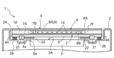
- 2 is a cross-sectional view of the main part showing the configuration of the panel member in the first embodiment, taken along line II-II in FIG. 1, and
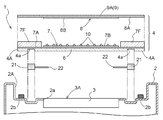
- FIG. 3 shows the configuration of the panel member in the first embodiment. It is an exploded sectional view of an important section.
- a mobile phone 1 having a protective panel 4 as an example of a panel member includes a liquid crystal or an organic EL or the like in a synthetic resin casing 2 having a display window 2A or the like formed on the front surface.
- the display window 2 ⁇ / b> A of the housing 2 is formed to be recessed so as to have a step allowing the fitting of the protective panel 4, and is provided inside the housing 2 on the bottom surface thereof.
- the display device 3 is opened so as to have an opening 2 a that exposes the display portion 3 ⁇ / b> A of the display device 3 and a frame-like support portion 2 b that supports the back surface peripheral edge portion 4 ⁇ / b> A of the protective panel 4.
- the shape and size of the display window 2A can be variously changed according to the shape and size of the protective panel 4, and the recessed depth of the display window 2A depends on the thickness of the protective panel 4 and the like.
- Various changes are possible, and the shape and size of the opening 2a in the display window 2A can be changed in accordance with the shape and size of the display 3A.
- the shape of the display window 2A, the opening 2a, the display unit 3A, and the protection panel 4 is rectangular or substantially rectangular, and the recessed depth of the display window 2A is set to the surface of the housing 2 and the protection panel 4. It is set to be the same height as the surface.
- the protection panel 4 can be selected from those having a so-called touch input function for detecting the XY coordinates as the operation position based on a touch operation on the protection panel 4 and those not having the touch input function.
- a touch input function it can be selected from a resistance film method, a capacitance method, an electromagnetic induction method, and the like.
- an example having a resistive film type touch input function will be described.
- the protective panel 4 includes a support plate 6 formed using a resin or glass having excellent transparency and rigidity, a lower electrode film 7 bonded to the upper surface of the support plate 6, and the lower electrode.
- the upper electrode film 8 disposed so as to have an air layer above the film 7 and the design sheet 9 bonded to the upper surface of the upper electrode film 8 have a function as a resistive film type touch panel A. Composed.
- the resin used for the support plate 6 is polycarbonate resin (PC), methacrylic resin (PMMA), acrylonitrile-styrene copolymer resin (AS), acrylonitrile-butadiene-styrene copolymer resin (ABS), cellulose propionate.
- Resin (CP), polystyrene resin (PS), polyester resin, and polyethylene resin (PE) can be selected from resins with excellent transparency and rigidity, especially polycarbonate resin (PC) and methacrylic resin (PMMA) with excellent transparency. It is preferable to use it.
- the glass used for the support plate 6 include soda glass, borosilicate glass, and tempered glass.
- the thickness of the support plate 6 can be selected from the range of 0.5 to 3.0 mm, and preferably 1.0 mm.
- the lower electrode film 7 has a pair of parallel electrodes positioned on two opposite sides of the rectangular transparent conductive film 7B and the transparent conductive film 7B on the upper surface of the transparent insulating substrate 7A.
- a lower bus bar 7C, a pair of routing circuits 7D positioned around the transparent conductive film 7B, a pair of connecting electrodes 7E, and a frame-like adhesive layer 7F are formed.
- the upper electrode film 8 has a rectangular transparent conductive film 8 ⁇ / b> B on the lower surface of a flexible transparent insulating substrate 8 ⁇ / b> A having a property of bending when pressed with a finger or the like.
- a pair of parallel upper bus bars 8C positioned on two opposite sides of the transparent conductive film 8B, a pair of routing circuits 8D positioned around the transparent conductive film 8B, and a pair of connecting electrodes 8E are formed.
- the transparent insulating base material 7A of the lower electrode film 7 and the flexible transparent insulating base material 8A of the upper electrode film engineering plastics such as polycarbonate, polyamide and polyetherketone, acrylic and polyethylene terephthalate
- a transparent film such as polybutylene terephthalate can be used.
- the transparent conductive films 7B and 8B of the lower electrode film 7 and the upper electrode film 8 metal oxide films such as tin oxide, indium oxide, antimony oxide, zinc oxide, cadmium oxide, and indium tin oxide (ITO), these metals
- metal oxide films such as tin oxide, indium oxide, antimony oxide, zinc oxide, cadmium oxide, and indium tin oxide (ITO)
- ITO indium tin oxide
- composite films mainly composed of oxides or metal films such as gold, silver, copper, tin, nickel, aluminum, and palladium.
- the transparent conductive films 7B and 8B may be formed in a multilayer of two or more layers.
- Examples of methods for forming the transparent conductive films 7B and 8B include a vacuum deposition method, a sputtering method, an ion plating method, and a CVD method.
- a dot-shaped spacer 10 can be formed.
- the spacer 10 can be a transparent photocurable resin such as epoxy acrylate or urethane acrylate, or a transparent thermosetting resin such as polyester or epoxy.
- the formation method of the spacer 10 includes a printing method such as screen printing and a photo process.
- the lower bus bar 7C, the upper bus bar 8C, the routing circuits 7D and 8D, and the connection electrodes 7E and 8E can be formed using a metal such as gold, silver, copper, nickel, or a conductive paste such as carbon.
- these forming methods include screen printing, offset printing, gravure printing, flexographic printing, and other printing methods, a photoresist method, and a brush coating method.
- the lower bus bar 7C and the upper bus bar 8C are formed at the end of the transparent insulating base material 7A or the flexible transparent insulating base material 8A as much as possible, and the transparent insulating base material 7A and the flexible transparent insulating base material are formed. In general, an area where the lower bus bar 7C and the upper bus bar 8C are not formed is as wide as possible at the center of 8A.
- the design sheet 9 is configured by forming a hard coat layer (not shown) on the upper surface of the flexible transparent insulating substrate 9A and forming a pattern layer and an adhesive layer (not shown) on the lower surface.
- engineering plastics such as polycarbonate, polyamide, and polyether ketone, and transparent films such as acrylic, polyethylene terephthalate, and polybutylene terephthalate can be used.
- the thickness of the flexible transparent insulating substrate 9A can be selected from the range of 50 to 200 ⁇ m, and is preferably 100 to 125 ⁇ m.
- the material used for the hard coat layer of the design sheet 9 includes an inorganic material such as a siloxane-based resin, or an organic material such as an acrylic epoxy-based or urethane-based thermosetting resin or an acrylate-based photocurable resin.
- the thickness of the hard coat layer is suitably about 1 to 7 ⁇ m.
- the hard coat layer As a method for forming the hard coat layer, a coating method such as roll coating or spray coating, or a normal printing method such as screen printing, offset printing, gravure printing or flexographic printing may be used. Further, the hard coat layer may be directly formed on the upper surface of the flexible transparent insulating substrate 9A on which the pattern layer and the adhesive layer are directly formed on the lower surface, or the pattern layer and the adhesive layer are directly formed on the lower surface.
- the flexible transparent insulating base material 9A may be formed on a different flexible transparent insulating base material, and the two flexible transparent insulating base materials may be bonded together.
- Light reflection such as, for example, subjecting the design sheet 9 to irregularities on the flexible transparent insulating substrate 9A or the hard coat layer, or mixing fine particles such as silica or alumina as extender pigments in the hard coat layer. You may make it perform the non-glare process for prevention.
- a normal printing method such as screen printing, offset printing, gravure printing, flexographic printing, or the like may be used.
- the offset printing method and the gravure printing method are suitable for performing multicolor printing and gradation expression.
- the pattern layer may be composed of a metal thin film layer or a combination of a pattern printing layer and a metal thin film layer.
- the metal thin film layer expresses metallic luster as a pattern layer, and is formed by a vacuum deposition method, a sputtering method, an ion plating method, a plating method, or the like.
- a metal such as aluminum, nickel, gold, platinum, chrome iron, copper, tin, indium, silver, titanium, lead, or zinc, or an alloy or compound thereof is used depending on the metallic luster color to be expressed.
- the film thickness of the metal thin film layer is generally about 0.05 ⁇ m.
- a heat-sensitive or pressure-sensitive resin suitable for the flexible transparent insulating substrate 8A of the upper electrode film 8 and the flexible transparent insulating substrate 9A of the design sheet 9 is appropriately used.
- the flexible transparent insulating bases 8A and 9A are polycarbonate or polyamide, polyacrylic resin, polystyrene resin, polyamide resin or the like may be used.
- the bases 8A and 9A are acrylic or polyethylene terephthalate, vinyl chloride, vinyl acetate, acrylic copolymer, or the like may be used.
- a normal printing method such as screen printing, offset printing, gravure printing, flexographic printing, or the like may be used.
- an ultraviolet curable acrylic hard coat is applied on one side of a flexible transparent insulating substrate 8A made of a 75 ⁇ m thick roll-shaped polyethylene terephthalate film (hereinafter abbreviated as PET film) using a roll coater. Then, after obtaining a PET film with a single-side hard coat, an indium tin oxide film (hereinafter abbreviated as ITO film) is formed on the hard coat surface by sputtering. Next, after cutting into a sheet shape so that the vertical and horizontal lengths have predetermined dimensions, an etching resist is applied in a pattern by screen printing on the ITO film, and an unnecessary ITO film is formed with sulfuric acid. Is removed to form a rectangular transparent conductive film 8B.
- PET film polyethylene terephthalate film
- ITO film indium tin oxide film
- the resist is removed by alkali cleaning, and a pair of parallel upper bus bars 8C, a pair of routing circuits 8D, and a pair of connection electrodes are formed by screen printing using silver paste on the two opposite sides and the periphery of the transparent conductive film 8B. 8E. Thereby, the upper electrode film 8 is obtained.
- an ultraviolet curable acrylic hard coat is applied to both sides of a flexible transparent insulating substrate 9A made of a roll-shaped PET film having a thickness of 125 ⁇ m using a roll coater, and PET with a double-sided hard coat is provided. Get a film. Then, cut into a sheet shape so that the length and width are the same dimensions as the upper electrode film 8, a pattern layer on one side, and an adhesive layer made of a transparent adhesive mainly composed of an acrylate ester, It is formed by gravure printing. Thereby, the design sheet 9 is obtained.
- the entire surface of the obtained upper electrode film 8 and the design sheet 9 is placed so that the non-ITO film forming surface of the upper electrode film 8 and the pattern layer surface of the design sheet 9 face each other through the adhesive layer of the design sheet 9. Paste together.
- an ultraviolet curable acrylic hard coat is applied to both surfaces of a transparent insulating substrate 7A made of a roll-shaped polycarbonate film (hereinafter abbreviated as PC film) having a thickness of 100 ⁇ m by a roll coater.
- PC film a roll-shaped polycarbonate film
- an ITO film is formed on one side by sputtering.
- an etching resist is applied in a pattern by screen printing on the ITO film, and the unnecessary ITO film is coated with sulfuric acid.
- the rectangular transparent conductive film 7B is formed by removing.
- a plurality of fine dot-shaped spacers 10 are formed on the entire surface of the transparent conductive film 7B by screen printing using an epoxy acrylate-based thermosetting resin.
- a pair of parallel lower bus bars 7C, a pair of routing circuits 7D, and a pair of connecting electrodes 7E are formed on the sides and around by screen printing using silver paste.
- a pressure-sensitive adhesive in which nickel-plated resin beads are dispersed is applied to the pair of connection electrodes 7E and the two connection sites 7G for the connection electrodes 8E of the upper electrode film 8 by screen printing.
- Adhesive ink mainly composed of an acrylate ester is applied by screen printing to the peripheral portion excluding those portions to form a frame-shaped adhesive layer 7F. Thereby, the lower electrode film 7 is obtained.
- the lower electrode film 7 bonded with the support plate 6 and the upper electrode film 8 bonded with the design sheet 9 are opposed to each other with the transparent conductive films 7B and 8B through the air layer, and the lower bus bar 7C.
- the upper bus bar 8C are orthogonally crossed and bonded via the adhesive layer 7F of the lower electrode film 7 so that the formation position of the connection electrode 8E of the upper electrode film 8 and the formation position of the corresponding through hole 11 coincide with each other. Match.
- a flexible printed circuit (hereinafter abbreviated as FPC) is produced with a film in which a circuit made of copper foil is formed on one side of a polyimide film, and hole processing is performed on an end electrode portion of the FPC. And a through hole 11 of the support plate 6 are made to coincide with each other, and a metal pin is inserted by an ultrasonic press-fitting device so that a touch input signal can be taken out on the non-lower electrode film application surface of the support plate 6. . Thereby, the protection panel 4 having a resistive film type touch input function is obtained.
- FPC flexible printed circuit
- a control unit (not shown) is provided inside the housing 2 and detects a pressing operation of the protection panel 4 in response to a signal from a pressure-sensitive member (not shown) provided on the protection panel 4.
- the control unit detects a pressing operation of the protection panel 4
- the control unit applies a predetermined driving voltage to the piezoelectric element 22, which is an example of a vibration element, and expands and contracts the piezoelectric element 22.
- the protection panel 4 is set to vibrate by the expansion and contraction of the piezoelectric element 22.
- FIG. 7 is a perspective view showing the mounting structure of the panel member and the vibration element in the first embodiment.
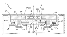
- FIG. 2 FIG. 3, FIG. 6 and FIG. 7, the mounting structure of the vibration elements 21 and 22 with respect to the protection panel 4 in the present embodiment will be described in detail.
- the vibration element includes a base portion 21 and a piezoelectric element 22 as a vibration member.
- the piezoelectric element 22 is first attached to a base portion 21 made of resin, and the base portion 21 is attached with a double-sided tape or an adhesive. Affix to the back of the protection panel 4.
- the vibration element including the base portion 21 and the piezoelectric element 22 is arranged in contact with the support portion 2b of the housing 2, the vibration of the vibration element is limited by the support portion 2b.
- a recess or the like is formed in the support portion 2b as necessary.
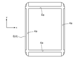
- a concave groove 4a is formed on the back surface of the protective panel 4 in parallel with two opposite sides of the peripheral edge 4A of the protective panel, and the base 21 is bonded to the concave groove 4a.
- the concave groove 4a of the protective panel 4 corresponds to a low-rigidity portion, and the protective panel 4 is easily bent at that portion, so that the vibration of the piezoelectric element 22 is easily transmitted also in the longitudinal (y coordinate) direction of the protective panel 4. .
- the protective panel vibrates without any problem if it is bonded to the central side of the protective panel 4 from the concave groove portion 4a of the protective panel 4. be able to.
- the base 21 of the piezoelectric element 22 is disposed in the concave groove 4a, there is an advantage that the entire protective panel 4 can be thinned by the depth of the concave groove 4a.
- the low-rigidity part of the protective panel 4 does not need to be formed on the entire peripheral edge 4A of the protective panel 4, and is protected, for example, in a corner or a small area that is less than one side of the protective panel. What is necessary is just to be formed in at least one part of the peripheral part 4A of the panel 4. FIG. If even a part of the peripheral edge 4A of the protective panel 4 is formed with a low rigidity part with reduced rigidity, only part of the protection panel 4 is likely to vibrate, and the position of the low rigidity part of the protection panel By changing the size and size, various vibration modes can be generated according to the application.
- the method for making a part of the protection panel 4 a low-rigidity part is not limited to the method of forming the concave groove 4a in the protection panel 4, and for example, a method of simply changing the thickness of the protection panel 4 Alternatively, a method of making the low-rigidity part by utilizing the characteristics of the material of the protective panel 4 without changing the thickness of the protective panel 4 may be adopted.
- the shape of the piezoelectric element 22 is not particularly limited, but is preferably a so-called cantilever shape that is a long vibration member that is cantilevered and supported by the base 21 as shown in FIG.
- the vibration of the protective panel 4 can be increased while pressing the contact surface between the piezoelectric element 22 and the protective panel 4 to a small area of only the base 21 of the piezoelectric element 22.
- the direction of the piezoelectric element 22 is not particularly limited, and is extended so as to be orthogonal to the concave groove portion 4a in FIG. 7, but may be extended so as to be parallel to the concave groove portion 4a as shown in FIG. Moreover, you may make it extend in the diagonal direction with respect to the concave groove part 4a.
- the protective panel that covers the display device which is an example of the panel member
- the panel member according to the present invention does not necessarily need to cover the display device. It can also be used for a flat-panel calculator operation surface and a computer keyboard.
- the panel member 4 is provided with the low rigidity portion by forming the concave groove portion 4a.
- the means for providing the low rigidity portion in a part of the panel member 4 is as follows.
- the present invention is not limited to this, and a low-rigidity part may be provided in a part of the panel member 4 by changing the layer structure of the panel member 4 or changing the material.
- the cantilever-shaped piezoelectric element 22 extends only on one side of the base 21, but the cantilever-shaped piezoelectric element 22 extends on both sides of the base 21 as shown in FIG. You may make it take out. By doing so, it is possible to adjust the magnitude of the vibration of the panel member 4, and it is also possible to expand the vibration region of the panel member 4 to the outer peripheral portion of the panel member outside the position of the base portion 21.
- the base 21 has substantially the same width as the concave groove 4a of the panel member 4, but the width of the concave groove 4a is wider than the width of the base 21 and is concave as shown in FIG. 9B.
- the piezoelectric element body 21 may be disposed in a part of the width of the groove 4a.
- the concave groove portion 4a formed on the back surface of the panel member 4 is not only one side portion of the peripheral edge portion 4A of the panel member 4, but also the two or three side portions or the entire periphery as shown in FIG. It may be provided. At this time, in order to further widen the vibration region of the panel member 4, the concave groove 4 a is preferably provided up to the peripheral edge of the panel member 4. Moreover, it becomes easy to change the degree of vibration of the panel member, etc. by forming a plurality of concave grooves 4a in the panel member 4 as necessary.
- the cantilever-shaped piezoelectric element 22 can be provided by extending from the corner of the panel member 4 in the longitudinal (y coordinate) direction and the lateral (x coordinate) direction. By doing so, the vibration of the panel member 4 can be increased, so that various modes of vibration can be applied to the panel member 4.
- the cantilever-shaped piezoelectric element 22 is provided at one corner of the panel member 4 and the other corner on the diagonal line, and the length of each piezoelectric element 22 is changed. You can also. By doing so, the resonance effect of vibration can be used, and the width of the vibration region of the panel member 4 and the magnitude of vibration can be adjusted.
- the panel member according to the present invention is effectively used for electronic devices such as a mobile phone, a smartphone, a PDA, a car navigation device, a digital camera, a digital video camera, a game machine, a tablet, a calculator, and a keyboard, and operates the electronic device with the panel member. It can be used to improve performance, reduce size, and reduce weight.
Landscapes
- Engineering & Computer Science (AREA)
- General Engineering & Computer Science (AREA)
- Theoretical Computer Science (AREA)
- Physics & Mathematics (AREA)
- General Physics & Mathematics (AREA)
- Human Computer Interaction (AREA)
- Quality & Reliability (AREA)
- Mechanical Engineering (AREA)
- Signal Processing (AREA)
- Position Input By Displaying (AREA)
- User Interface Of Digital Computer (AREA)
- Telephone Set Structure (AREA)
- Push-Button Switches (AREA)
Abstract
Description
これらのフォースフィードバック型タッチパネルは、対向する両面に一対の駆動電極が固着された圧電基板を、直接もしくは、駆動電極を介して、可動板又は支持基板に固着し、タッチパネルの入力操作面への押圧を検出した際に、一対の駆動電極に駆動電圧が印加されて伸縮する圧電基板により可動板又は支持基板を振動させている。
また、特許文献3では、加振ドライバが矩形の可動板の隅部に配置される構成であるので、一方向の振動が規制されることはないが、振動を大きくしたいときには、加振ドライバの数を増やす必要があった。
また、パネル部材の凹状溝部内に振動素子を取付けると、パネル部材の凹状溝部の深さの分だけ厚みが減ることとなるので、振動素子を含むパネル部材全体の厚みを薄くすることができる。その結果、パネル部材付き電子機器の小型化、軽量化を図ることもできる。
本発明に係わるパネル部材は、携帯電話機、スマートフォン、PDA、カーナビゲーション装置、デジタルカメラ、デジタルビデオカメラ、遊技機等のようなモバイル機器に用いられる。ここでは、パネル部材として携帯電話機に用いられる保護パネルを例示して説明する。
図1~図3に示すように、パネル部材の一例である保護パネル4を有する携帯電話機1は、前面に表示窓2Aなどが形成された合成樹脂製の筐体2に、液晶又は有機ELなどの表示部3Aを有する表示装置3、その表示装置3の表面を被覆し保護する保護パネル4、及び、複数の入力キー5などを備えて構成されている。
これによって、抵抗膜方式のタッチ入力機能を有する保護パネル4が得られる。
(1)上記実施形態1では、パネル部材の一例である、表示装置を被覆する保護パネルについて説明したが、本発明に係るパネル部材は、必ずしも表示装置を被覆する必要はなく、例えば、表示装置を有さない平板状の電卓操作面やコンピュータのキーボード等にも用いることができる。
2 筐体
2A 表示窓
2b 支持部
3 表示装置
3A 表示部
4 保護パネル(パネル部材)
4A 周縁部
4a 凹状溝部(低剛性部分)
21 基部
22 圧電素子(振動部材)
Claims (4)
- 接触式の情報入力機能を備え、周縁部に少なくとも一部に剛性を低下させた低剛性部分が形成され、
前記低剛性部分を含めて中央側に振動素子を有するパネル部材。 - 前記低剛性部分が凹状溝部である請求項1記載のパネル部材。
- 全体が矩形状であり、前記凹状溝部を少なくとも一辺に沿って設けてある請求項2記載のパネル部材。
- 前記振動素子が、基部と、当該基部から片持ちされた長尺状の振動部材とを備えた請求項1~3のいずれか一項に記載のパネル部材。
Priority Applications (2)
| Application Number | Priority Date | Filing Date | Title |
|---|---|---|---|
| CN200980152418.1A CN102265248A (zh) | 2008-12-26 | 2009-12-07 | 具有振动元件的面板部件 |
| US13/141,210 US20110304569A1 (en) | 2008-12-26 | 2009-12-07 | Panel Member Having Oscillating Element |
Applications Claiming Priority (2)
| Application Number | Priority Date | Filing Date | Title |
|---|---|---|---|
| JP2008-333924 | 2008-12-26 | ||
| JP2008333924A JP2010157037A (ja) | 2008-12-26 | 2008-12-26 | 振動素子を有するパネル部材 |
Publications (1)
| Publication Number | Publication Date |
|---|---|
| WO2010073509A1 true WO2010073509A1 (ja) | 2010-07-01 |
Family
ID=42287167
Family Applications (1)
| Application Number | Title | Priority Date | Filing Date |
|---|---|---|---|
| PCT/JP2009/006671 Ceased WO2010073509A1 (ja) | 2008-12-26 | 2009-12-07 | 振動素子を有するパネル部材 |
Country Status (6)
| Country | Link |
|---|---|
| US (1) | US20110304569A1 (ja) |
| JP (1) | JP2010157037A (ja) |
| KR (1) | KR20110098962A (ja) |
| CN (1) | CN102265248A (ja) |
| TW (1) | TW201030561A (ja) |
| WO (1) | WO2010073509A1 (ja) |
Cited By (2)
| Publication number | Priority date | Publication date | Assignee | Title |
|---|---|---|---|---|
| WO2012057214A1 (ja) * | 2010-10-27 | 2012-05-03 | 京セラ株式会社 | 電子機器、およびこれを備えた携帯端末 |
| WO2012063645A1 (ja) * | 2010-11-12 | 2012-05-18 | 京セラ株式会社 | 電子機器、およびこれを備えた携帯端末 |
Families Citing this family (30)
| Publication number | Priority date | Publication date | Assignee | Title |
|---|---|---|---|---|
| JPS58104428A (ja) * | 1981-12-16 | 1983-06-21 | Toshiba Corp | ガスタ−ビン燃焼器 |
| US8821915B2 (en) | 2002-08-09 | 2014-09-02 | Veroscience, Llc | Therapeutic process for the treatment of the metabolic syndrome and associated metabolic disorders |
| US9352025B2 (en) | 2009-06-05 | 2016-05-31 | Veroscience Llc | Combination of dopamine agonists plus first phase insulin secretagogues for the treatment of metabolic disorders |
| US8730182B2 (en) * | 2009-07-30 | 2014-05-20 | Immersion Corporation | Systems and methods for piezo-based haptic feedback |
| US8816981B2 (en) * | 2009-08-31 | 2014-08-26 | Nissha Printing Co., Ltd. | Mount structure of touch panel with vibration function |
| JP5287998B2 (ja) * | 2009-11-19 | 2013-09-11 | 株式会社村田製作所 | タッチパネル付き電子機器 |
| US9870053B2 (en) * | 2010-02-08 | 2018-01-16 | Immersion Corporation | Systems and methods for haptic feedback using laterally driven piezoelectric actuators |
| JP5597583B2 (ja) | 2011-03-28 | 2014-10-01 | 太陽誘電株式会社 | タッチパネル装置及び電子機器 |
| JP5962907B2 (ja) * | 2011-07-06 | 2016-08-03 | パナソニックIpマネジメント株式会社 | 電子機器 |
| WO2013057940A1 (ja) | 2011-10-19 | 2013-04-25 | パナソニック株式会社 | 電子機器 |
| WO2013099742A1 (ja) * | 2011-12-27 | 2013-07-04 | 株式会社村田製作所 | 触覚提示装置 |
| FR2985331B1 (fr) * | 2011-12-30 | 2014-04-25 | Dav | Dispositif de commande a retour haptique |
| JP5905312B2 (ja) * | 2012-03-27 | 2016-04-20 | 京セラ株式会社 | 音響装置 |
| WO2013168338A1 (ja) * | 2012-05-09 | 2013-11-14 | パナソニック株式会社 | 電子機器 |
| US20140209380A1 (en) * | 2013-01-30 | 2014-07-31 | Young Fast Optoelectronics Co., Ltd. | Assembling structure for flexible flat cable of touch panel |
| KR102025786B1 (ko) * | 2013-07-04 | 2019-09-27 | 삼성디스플레이 주식회사 | 표시 장치 |
| JP5904174B2 (ja) * | 2013-08-22 | 2016-04-13 | Smk株式会社 | タッチパネルの支持構造 |
| KR20150104415A (ko) * | 2014-03-05 | 2015-09-15 | 삼성전기주식회사 | 압전진동기판 |
| JP6137415B2 (ja) * | 2014-09-12 | 2017-05-31 | 株式会社村田製作所 | 触覚提示装置 |
| JP5956525B2 (ja) * | 2014-10-01 | 2016-07-27 | レノボ・シンガポール・プライベート・リミテッド | 入力装置 |
| JP6199847B2 (ja) * | 2014-11-12 | 2017-09-20 | 京セラ株式会社 | 触感呈示装置 |
| JP6086960B2 (ja) * | 2015-08-20 | 2017-03-01 | Necトーキン株式会社 | 入力装置 |
| JP6288387B2 (ja) * | 2015-10-05 | 2018-03-07 | 株式会社村田製作所 | 振動装置および触覚提示装置 |
| JP6111315B1 (ja) * | 2015-11-27 | 2017-04-05 | 京セラ株式会社 | 触感呈示装置 |
| CN105468220A (zh) * | 2015-12-25 | 2016-04-06 | 合肥工业大学 | 一种基于有源阵列的多点电阻触摸屏 |
| KR102384033B1 (ko) * | 2017-03-20 | 2022-04-06 | 엘지전자 주식회사 | 디스플레이 장치 |
| JP2018194923A (ja) * | 2017-05-12 | 2018-12-06 | アルプス電気株式会社 | 入力装置 |
| CN110121008A (zh) * | 2019-05-21 | 2019-08-13 | Oppo广东移动通信有限公司 | 振动方法、终端及存储介质 |
| EP4276585A1 (en) * | 2022-05-09 | 2023-11-15 | Aito BV | A haptic effect device |
| WO2024116684A1 (ja) * | 2022-11-28 | 2024-06-06 | パナソニックオートモーティブシステムズ株式会社 | 入力装置及びパネル |
Citations (3)
| Publication number | Priority date | Publication date | Assignee | Title |
|---|---|---|---|---|
| JPH09161602A (ja) * | 1995-12-04 | 1997-06-20 | Idec Izumi Corp | 薄型スイッチおよびスイッチ付表示パネル |
| JP2004334740A (ja) * | 2003-05-12 | 2004-11-25 | Alps Electric Co Ltd | 座標入力装置 |
| JP2005228161A (ja) * | 2004-02-13 | 2005-08-25 | Fujitsu Component Ltd | 平面板振動装置及びこれを用いたスイッチ |
Family Cites Families (6)
| Publication number | Priority date | Publication date | Assignee | Title |
|---|---|---|---|---|
| FI115861B (fi) * | 2001-11-12 | 2005-07-29 | Myorigo Oy | Menetelmä ja laite palautteen generoimiseksi |
| US7369115B2 (en) * | 2002-04-25 | 2008-05-06 | Immersion Corporation | Haptic devices having multiple operational modes including at least one resonant mode |
| JP3871991B2 (ja) * | 2002-09-30 | 2007-01-24 | Smk株式会社 | タッチパネル |
| JP2004350159A (ja) * | 2003-05-23 | 2004-12-09 | Alps Electric Co Ltd | 発音用の励振装置および前記励振装置を備えた電子機器 |
| JP2006031415A (ja) * | 2004-07-16 | 2006-02-02 | Alps Electric Co Ltd | 入力装置 |
| JP2006215738A (ja) * | 2005-02-02 | 2006-08-17 | Sony Corp | 振動伝達構造、触覚機能付きの入力装置及び電子機器 |
-
2008
- 2008-12-26 JP JP2008333924A patent/JP2010157037A/ja not_active Ceased
-
2009
- 2009-12-07 WO PCT/JP2009/006671 patent/WO2010073509A1/ja not_active Ceased
- 2009-12-07 KR KR1020117016992A patent/KR20110098962A/ko not_active Ceased
- 2009-12-07 US US13/141,210 patent/US20110304569A1/en not_active Abandoned
- 2009-12-07 CN CN200980152418.1A patent/CN102265248A/zh active Pending
- 2009-12-24 TW TW098144643A patent/TW201030561A/zh unknown
Patent Citations (3)
| Publication number | Priority date | Publication date | Assignee | Title |
|---|---|---|---|---|
| JPH09161602A (ja) * | 1995-12-04 | 1997-06-20 | Idec Izumi Corp | 薄型スイッチおよびスイッチ付表示パネル |
| JP2004334740A (ja) * | 2003-05-12 | 2004-11-25 | Alps Electric Co Ltd | 座標入力装置 |
| JP2005228161A (ja) * | 2004-02-13 | 2005-08-25 | Fujitsu Component Ltd | 平面板振動装置及びこれを用いたスイッチ |
Cited By (6)
| Publication number | Priority date | Publication date | Assignee | Title |
|---|---|---|---|---|
| WO2012057214A1 (ja) * | 2010-10-27 | 2012-05-03 | 京セラ株式会社 | 電子機器、およびこれを備えた携帯端末 |
| JPWO2012057214A1 (ja) * | 2010-10-27 | 2014-05-12 | 京セラ株式会社 | 電子機器、およびこれを備えた携帯端末 |
| US9007320B2 (en) | 2010-10-27 | 2015-04-14 | Kyocera Corporation | Electronic equipment and mobile terminal provided with same |
| WO2012063645A1 (ja) * | 2010-11-12 | 2012-05-18 | 京セラ株式会社 | 電子機器、およびこれを備えた携帯端末 |
| JPWO2012063645A1 (ja) * | 2010-11-12 | 2014-05-12 | 京セラ株式会社 | 電子機器、およびこれを備えた携帯端末 |
| US9170652B2 (en) | 2010-11-12 | 2015-10-27 | Kyocera Corporation | Electronic device and portable terminal provided with same |
Also Published As
| Publication number | Publication date |
|---|---|
| US20110304569A1 (en) | 2011-12-15 |
| CN102265248A (zh) | 2011-11-30 |
| JP2010157037A (ja) | 2010-07-15 |
| TW201030561A (en) | 2010-08-16 |
| KR20110098962A (ko) | 2011-09-02 |
Similar Documents
| Publication | Publication Date | Title |
|---|---|---|
| WO2010073509A1 (ja) | 振動素子を有するパネル部材 | |
| JP5306944B2 (ja) | スピーカ兼用タッチパネルの実装構造 | |
| US8816981B2 (en) | Mount structure of touch panel with vibration function | |
| JP5306945B2 (ja) | 触感フィードバック型タッチパネルの実装構造 | |
| TWI474249B (zh) | 具備觸控輸入功能的保護面板 | |
| TWI472285B (zh) | 附有保護面板之電子機器 | |
| JP4880723B2 (ja) | 押圧検出機能を有する抵抗膜式タッチパネル | |
| TWI425461B (zh) | Electronic machine with protective panel | |
| JP4753918B2 (ja) | アナログ抵抗膜方式のタッチ入力機能を備えた保護パネル | |
| WO2010074144A1 (ja) | 電子機器表窓のタッチ入力機能付き保護パネルとその製造方法 | |
| JP4875182B2 (ja) | 保護パネル及び電子機器 | |
| JP2008287670A (ja) | 電子機器表示窓のタッチ入力機能付き保護パネル | |
| JP5258994B2 (ja) | 電子機器、およびこれを備えた携帯端末に関する。 | |
| JP2011034282A (ja) | 入力感が得られる入力機能付き保護パネル | |
| JP2008262289A (ja) | 電子機器表示窓のタッチ入力機能付き保護パネル |
Legal Events
| Date | Code | Title | Description |
|---|---|---|---|
| WWE | Wipo information: entry into national phase |
Ref document number: 200980152418.1 Country of ref document: CN |
|
| 121 | Ep: the epo has been informed by wipo that ep was designated in this application |
Ref document number: 09834324 Country of ref document: EP Kind code of ref document: A1 |
|
| NENP | Non-entry into the national phase |
Ref country code: DE |
|
| ENP | Entry into the national phase |
Ref document number: 20117016992 Country of ref document: KR Kind code of ref document: A |
|
| WWE | Wipo information: entry into national phase |
Ref document number: 13141210 Country of ref document: US |
|
| 122 | Ep: pct application non-entry in european phase |
Ref document number: 09834324 Country of ref document: EP Kind code of ref document: A1 |