WO2010024082A1 - 欠陥検査システムおよび欠陥検査方法 - Google Patents
欠陥検査システムおよび欠陥検査方法 Download PDFInfo
- Publication number
- WO2010024082A1 WO2010024082A1 PCT/JP2009/063445 JP2009063445W WO2010024082A1 WO 2010024082 A1 WO2010024082 A1 WO 2010024082A1 JP 2009063445 W JP2009063445 W JP 2009063445W WO 2010024082 A1 WO2010024082 A1 WO 2010024082A1
- Authority
- WO
- WIPO (PCT)
- Prior art keywords
- camera
- plate
- bright
- defect inspection
- light
- Prior art date
- Legal status (The legal status is an assumption and is not a legal conclusion. Google has not performed a legal analysis and makes no representation as to the accuracy of the status listed.)
- Ceased
Links
Images




Classifications
-
- G—PHYSICS
- G01—MEASURING; TESTING
- G01N—INVESTIGATING OR ANALYSING MATERIALS BY DETERMINING THEIR CHEMICAL OR PHYSICAL PROPERTIES
- G01N21/00—Investigating or analysing materials by the use of optical means, i.e. using sub-millimetre waves, infrared, visible or ultraviolet light
- G01N21/84—Systems specially adapted for particular applications
- G01N21/88—Investigating the presence of flaws or contamination
- G01N21/89—Investigating the presence of flaws or contamination in moving material, e.g. running paper or textiles
- G01N21/8901—Optical details; Scanning details
-
- G—PHYSICS
- G01—MEASURING; TESTING
- G01N—INVESTIGATING OR ANALYSING MATERIALS BY DETERMINING THEIR CHEMICAL OR PHYSICAL PROPERTIES
- G01N21/00—Investigating or analysing materials by the use of optical means, i.e. using sub-millimetre waves, infrared, visible or ultraviolet light
- G01N21/84—Systems specially adapted for particular applications
- G01N21/88—Investigating the presence of flaws or contamination
- G01N21/89—Investigating the presence of flaws or contamination in moving material, e.g. running paper or textiles
- G01N21/892—Investigating the presence of flaws or contamination in moving material, e.g. running paper or textiles characterised by the flaw, defect or object feature examined
- G01N21/896—Optical defects in or on transparent materials, e.g. distortion, surface flaws in conveyed flat sheet or rod
-
- G—PHYSICS
- G01—MEASURING; TESTING
- G01N—INVESTIGATING OR ANALYSING MATERIALS BY DETERMINING THEIR CHEMICAL OR PHYSICAL PROPERTIES
- G01N21/00—Investigating or analysing materials by the use of optical means, i.e. using sub-millimetre waves, infrared, visible or ultraviolet light
- G01N21/84—Systems specially adapted for particular applications
- G01N21/88—Investigating the presence of flaws or contamination
- G01N21/95—Investigating the presence of flaws or contamination characterised by the material or shape of the object to be examined
- G01N21/958—Inspecting transparent materials or objects, e.g. windscreens
-
- G—PHYSICS
- G01—MEASURING; TESTING
- G01N—INVESTIGATING OR ANALYSING MATERIALS BY DETERMINING THEIR CHEMICAL OR PHYSICAL PROPERTIES
- G01N21/00—Investigating or analysing materials by the use of optical means, i.e. using sub-millimetre waves, infrared, visible or ultraviolet light
- G01N21/84—Systems specially adapted for particular applications
- G01N21/88—Investigating the presence of flaws or contamination
- G01N21/89—Investigating the presence of flaws or contamination in moving material, e.g. running paper or textiles
- G01N21/8901—Optical details; Scanning details
- G01N2021/8905—Directional selective optics, e.g. slits, spatial filters
Definitions
- the present invention relates to a defect inspection system and a defect inspection method for detecting defects existing in a plate-like body such as a transparent glass plate.
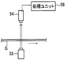
- a linear light source 52 longer than the width of the glass plate G is provided on one side of the conveyed glass plate G, and light is projected onto the glass plate G with a predetermined light intensity.
- a bright field image of the transmitted light that has passed through G is taken by a line sensor type camera 54 provided on the other side, and this image is sent to the processing unit 56.
- the processing unit 56 extracts a dark area included in the bright field image and extracts it as a defective area.
- the linear light source 52 that projects light onto the glass substrate G is made to be substantially parallel light using a long and narrow slit extending in the width direction of the glass plate G in order to capture an image with a line sensor type camera 54. Thereby, the defect of the glass plate G conveyed can be detected.
- Patent Document 1 proposes a defect detection method for detecting a defect in a transparent plate.
- this detection method an illuminator that illuminates at an angle close to perpendicular to the plane of the plate-like body and an illuminator that illuminates at an angle close to parallel are provided, and image processing of an image obtained using these illuminators is performed.
- the present invention provides a defect inspection system and a defect inspection method that can be used effectively in a production line for a plate-like body having transparency, such as a glass plate, in order to solve the above problems.
- An object is to provide a defect inspection system and a defect inspection method capable of efficiently determining and detecting whether or not a defect exists in a body, and to provide a method for manufacturing a plate-like body using this inspection method.
- the present invention provides a defect inspection system for detecting a defect present in a transparent plate-like body, the first linear light source projecting on the surface of the plate-like body, A first camera that collects the transmitted light that has passed through the plate-like body and captures a bright-field image, and a front surface of the first camera in the optical path of the transmitted light of the first camera.
- a defect inspection system comprising: a processing device for determining whether to perform or not. To.
- the first light source is a linear light source
- an imaging lens for forming an image of a plate-like body is provided on the front surface of the light receiving surface of the first camera.
- the first camera is defined as an illumination light emission effective angle that is a half of the divergence angle of the transmitted light beam of the first light source from the light source to the light receiving surface of the first camera through the imaging lens.
- a value representing the light emission directivity of the first light source is defined as an angle of view which is a half of the expected angle of the visual field range from the position of the light receiving surface to the irradiation surface of the first light source through the imaging lens.
- ⁇ When ⁇ is set, a value obtained by multiplying the ratio of the angle of view with respect to the illumination light emission effective angle by a value ⁇ representing the light emission directivity of the first light source is greater than 2, a first condition, and the optical path shielding member From the light receiving surface that can be a surface orthogonal to the optical axis of the imaging lens at the transmitted light passage
- the second condition is such that the area of the portion where the circle of confusion is blocked by the optical path shielding member is 43 to 57% of the area of the circle of confusion.
- the first light source, the imaging lens, and the first camera are set.
- the aperture value of the first camera, the distance between the first camera and the plate, the plate and the first so as to satisfy the first condition and the second condition A distance to the light source and a light emission width of the first light source are determined.
- arranging so as to face each other means arranging the light receiving elements of the first camera so as to be positioned in the direction of the maximum light intensity of the first light source with the glass plate G interposed therebetween.
- the plate-shaped body to be inspected by the first defect inspection apparatus receives illumination light reflected from the plate-shaped body and inspects the defect.
- the second defect inspection apparatus has a second light source for irradiating illumination light onto the surface of the plate-like body, and collects reflected light emitted from the surface of the plate-like body.
- a second camera provided on the same side as the second light source as viewed from the plate-like body, and the processing device is photographed by the second camera. If a dark area in the image reflected by the plate-like body is extracted from the bright-field reflected image, and this dark area is close to the bright area, it is determined that a defect exists in the plate-like body. It is preferable.
- the processing device determines the thickness of the plate-like body based on the positional deviation between the dark portion area in the image reflected by the plate-like body and the dark portion in the image reflected by the other surface of the plate-like body. It is preferable to obtain defect position information in the vertical direction.
- the plate-like body is transported and moved in one direction, and the first defect inspection apparatus and the second defect inspection apparatus are the first defect inspection apparatus and the second defect inspection apparatus. It is preferable that it is provided on the upstream side. However, the first defect inspection apparatus may be provided on the downstream side of the second defect inspection apparatus. Here, it is preferable that the first defect inspection apparatus and the second defect inspection apparatus are provided adjacent to each other in the transport direction. This is because, when the distance between the first defect inspection apparatus and the second defect inspection apparatus is shorter, defect detection and identification can be processed within a shorter time than when the distance is longer.
- the present invention is a defect inspection method for detecting a defect present in a transparent plate-like body, wherein the plate-like body is projected from a first linear light source onto the surface of the plate-like body.
- a light path shielding in the form of a knife edge is provided at the position in front of the first camera in the optical path of the transmitted light of the first camera.
- a bright part is picked up from a bright-field image by setting a signal value higher than the signal value of the background component of the bright-field image as a threshold from the bright-field image photographed by the first camera.
- a bright area is extracted as a result of the search, it is determined whether or not a defect area exists in the plate using the bright area caused by this refractive error.
- a feature defect inspection method is provided.
- the present invention is not particularly limited by the thickness of the plate-like body.
- a flat panel display FPD
- the present invention is applied to a liquid crystal display (LCD) including a thin plate type, and the thickness is 0.1.
- LCD liquid crystal display
- PDP plasma display panels
- PDP plasma display panels
- a knife edge-shaped optical path shielding member is provided at a position in front of the first camera in the optical path of the transmitted light of the first camera, and the first camera captures the image. From the bright field image, a bright area is extracted from the bright field image using a signal value higher than the signal value of the background component of the bright field image as a threshold, and the extracted bright area is By using it for detecting a defect area existing in the plate-like body, it is possible to efficiently determine and detect whether the defect exists in the plate-like body.
- the optical system of the first camera is set so as to satisfy the second condition in which the area of the portion where the circle of confusion is blocked is set to 43 to 57% of the area of the circle of confusion.
- the defect inspection can be performed more effectively by providing the first light source used for measurement and the first camera so as to face each other across the glass plate G.
- the second light source for irradiating illumination light onto the surface of the plate-like body, and the reflected light obtained by irradiating and reflecting on the surface of the plate-like body is collected, and a bright field reflection image is photographed.
- the second camera provided on the same side as the second light source when viewed from the body, and the processing device is configured to obtain a plate-like body from a bright-field reflection image photographed by the second camera.
- the dark area in the image reflected by the surface is extracted and this dark area is in close proximity to the bright area, the plate-like body is formed based on the positional deviation between the real image of the defect and the mirror image of the defect. Position information in the thickness direction of the defect located can be obtained.
- a defect inspection system 10 shown in FIG. 1 includes a first defect inspection device 12, a second defect inspection device 14, and a processing device 16.
- the first defect inspection device 12 and the second defect inspection device 14 are provided in this order from the upstream side along the conveyance path of the glass sheet G.
- the processing device 16 is a device that processes the images obtained by the first defect inspection device 12 and the second defect inspection device 14 and performs defect detection.
- the glass plate G is a long plate material that is taken out of the melting furnace and has a predetermined thickness, and is conveyed on a plurality of drive rollers 18 provided in a conveyance path.
- the first defect inspection apparatus 12 is an apparatus that is located on the most upstream side of the defect inspection system 10 on the conveyance side and inspects defects on the glass sheet G. Specifically, the first defect inspection apparatus 12 transmits the first linear light source 20 that projects light from the drive roller 18 side (lower side) to the surface of the glass plate G and the glass plate G that has passed through.
- a first camera 22 that collects light and captures a bright-field image, and a knife-edge optical path provided at a position in front of the first camera 22 in the optical path of the transmitted light of the first linear light source 20 And a shielding member 24.
- the first linear light source 20 is an LED light source that emits substantially parallel light, and the exit of the first linear light source 20 is along the width direction of the glass plate G (the direction perpendicular to the paper surface in FIG. 1). It extends linearly.
- the exit of the first linear light source 20 is provided, for example, at a position 100 to 900 mm away from the surface of the glass plate G, and the width L (see FIG. 2) along the light source transport direction is, for example, 1 to 20 mm.
- the 1st linear light source 20 is provided away from the surface of the glass plate G at the point which does not require high position accuracy.
- the type of light in the LED light source is not particularly limited, and white is preferably used, but may be red, blue, green, or the like.
- the LED light source includes a light emitting source (not shown) that emits light, a Fresnel lens (not shown) that makes emitted light substantially parallel light, and a diffusion plate (not shown) that makes light intensity substantially uniform. And a slit plate (not shown) for narrowing the emission of light. Accordingly, the first linear light source 20 emits substantially parallel light having substantially uniform light intensity.
- the light intensity is not necessarily uniform and the light cannot be made parallel, the light intensity has directional characteristics, and the light spreads.
- a value representing the directivity is ⁇ .
- the first camera 22 is a line sensor type camera that is provided at a position facing the first linear light source 20 with the glass plate G interposed therebetween and reads transmitted light that has passed through the glass G directly on the light receiving surface.
- a plurality of first cameras 22 are provided in the direction perpendicular to the paper surface in FIG. 1 and photograph the same position in the transport direction.
- the plurality of cameras have mutually different viewing ranges in the width direction of the glass plate G. In the inspection part of the glass plate G, it is arranged so that there is no non-inspection area.
- the first camera 22 is provided so that the light receiving surface comes to a position where the focusing lens 23 (see FIG.
- the first camera 22 includes an optical system including an imaging lens 23 and a diaphragm that adjusts an aperture, which is not illustrated.
- the image data obtained by the first camera 22 is sequentially sent to the processing device 16 every time it is read in a line shape.
- the optical path shielding member 24 is a knife edge-shaped member that blocks a part of the optical path at the position of the front surface of the first camera 22 in the optical path of the transmitted light from the glass G.
- the tip portion in the optical path is sharpened so as to form a blade.
- the optical path shielding member 24 is provided at a position on the front surface of the optical system (imaging lens 23) of the first camera 22, for example, at a position 1 to 5 mm away.
- the part that holds the optical path shielding member 24 is provided with a mechanism that allows the optical path shielding member 24 to move in the X direction so as to cross the optical path.
- a circle of confusion representing the field of view as viewed from the light receiving surface which can be a surface orthogonal to the optical axis of the imaging lens 23 in the first camera 22 at the passing position of the transmitted light of the optical path shielding member 24, is determined.
- the area of the portion where the circle of confusion is blocked by the optical path shielding member 24 corresponds to 43 to 57%, preferably about 50%, of the area of the circle of confusion. If it is less than 43%, a bright field described later is unlikely to occur in the bright field image, and if it exceeds 57%, a dark field image tends to be formed.
- Such a range for blocking the optical path can be realized by adjusting the distance between the light shielding member 24 and the glass plate G and the aperture value of the first camera 22, for example.
- the range for blocking the optical path can be realized by setting the range for blocking the optical path to this range, as will be described later, the bright region is efficiently formed in the vicinity of the dark region created by defects such as bubbles existing in the bright field image. Because.
- the effective illumination emission angle ⁇ is a light flux of transmitted light from the first linear light source 20 that reaches the light receiving surface of the light receiving element of the first camera 22 through the imaging lens 23 from the first linear light source 20.
- the angle of view ⁇ ranges from the position of the light receiving surface of the light receiving element of the first camera 22 through the imaging lens 23 (using the effective aperture d of the lens) to the irradiation surface of the first linear light source 20. Is half of the prospective angle.
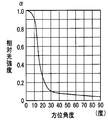
- the value ⁇ representing the light emission directivity of the first linear light source 20 has an azimuth angle with the direction perpendicular to the irradiation surface of the light source as the azimuth angle of 0 degrees on the horizontal axis, as shown in FIG.
- the vertical axis represents the average value of relative light intensity when the maximum light intensity value is 1.
- the first camera 22 is disposed so that the light receiving element of the first camera 22 faces the first linear light source 20 with the glass plate G interposed therebetween.
- d in FIG. 2 is an effective aperture of the imaging lens 23 and is represented by f / F (f is a focal length, and F is an F value).
- the illumination emission effective angle ⁇ and the angle of view ⁇ used in the present invention are geometrically determined based on the setting and arrangement of each device as shown in FIG.
- Such a first defect inspection device 12 makes it possible to easily detect defects such as fine bubbles present on the glass plate G.
- the second defect inspection apparatus 14 includes a second light source 28 and a second camera 30.
- the 2nd defect inspection apparatus 14 illuminates a glass plate from one side with respect to the glass plate G test
- the detection result of the second defect inspection apparatus 14 is combined and comprehensively evaluated, thereby more accurately identifying defects present in the glass plate G. Now it can be done accurately.
- the second light source 28 is an LED light source that emits substantially parallel light to the surface of the glass plate G, and makes light incident from a direction inclined with respect to the surface of the glass plate G.
- the second light source 28 extends in a direction perpendicular to the paper surface of FIG.
- the type of light in the LED light source used for the second light source 28 is not particularly limited, and white is preferably used, but may be red, blue, green, or the like.
- the LED light source includes a light emitting source (not shown) that emits light, a Fresnel lens (not shown) that makes emitted light substantially parallel light, and a diffusion plate (not shown) that makes light intensity substantially uniform. And a slit plate (not shown) for narrowing the emission of light.
- the second linear light source 28 emits substantially parallel light having substantially uniform light intensity.
- the second camera 30 is a line sensor type camera that collects reflected light emitted from the surface of the glass G and shoots a bright field reflected image.
- the second camera 30 is provided on the same side as the second light source 28 when viewed from the glass plate G.
- the image photographed by the second camera 30 is an image that is illuminated by the second light source 28 and reflected by the back surface of the glass G, and is an image in which a defect area existing in the glass plate G becomes a dark part.
- the defect region passes through the optical path of the reflected light.
- the glass plate G And a mirror image of defects formed by reflection on the back surface of the film.
- the image data obtained by the second camera 30 is sent to the processing device 16 every time it is read in a line shape.
- the processing device 16 uses the image data sent from the first defect inspection device 12 and the second defect inspection device 14 to detect a defect on the glass plate G, identify the type of the defect, and also detect the defect glass. It is also an apparatus for specifying the position of the plate G in the thickness direction.
- a display 32 is connected to the processing device 16, and the display 32 includes images, defect detection results, identification results, or defect positions obtained by the first defect inspection device 12 and the second defect inspection device 14. The specific result is displayed on the screen.
- the image obtained by the first defect inspection apparatus 12 is a bright field image, and the defect of the glass plate G appears as a dark part in the image due to irregular reflection of the defect region.
- a knife-edge-shaped optical path shielding member 24 that blocks a part of the optical path is provided immediately before the optical system of the first camera 22, so that the optical path shielding member 24 allows the image to be displayed.
- a bright area is formed so as to face the dark area in the vicinity or to face and contact each other. The bright portion is generated due to a refractive error in the defective portion, and has a higher brightness than the background portion of the bright field image.
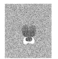
- FIG. 4A is a schematic diagram of an example of a defect image when the optical path shielding member 24 is in the optical path. As shown in FIG. 4A, a bright part is formed that faces the dark part region in close proximity.
- FIG. 4B is a schematic diagram of an example of a defect image when the optical path shielding member 24 does not exist in the optical path (does not block light). As shown in FIG. 4B, the bright part that faces the dark part region in the vicinity is not formed. In the bright field image, as shown in FIG. 4A, the bright part is formed so as to face the dark part region in close proximity to the glass plate G due to bubbles or foreign substances existing on the surface or inside of the glass plate G.
- the processing device 16 sets a threshold value higher than the value of the image data of the background portion in the bright field image, and extracts an area that is equal to or larger than the threshold value as the bright part area. Since the image data sent from the first camera 22 is one-dimensional image data that has passed through the inspection position and is read by the line sensor type camera, the processing device 16 has a plurality of lines (for example, 500 lines). ) Image data is accumulated and an image of a certain surface area is obtained, the extraction of the bright area is started. The position information of the extracted bright area is used as follows when detecting a defective area existing on the glass plate G.
- the image data obtained by the second defect inspection apparatus 14 and sent to the processing apparatus 16 is data of a bright field reflection image, and is an image in which a defective portion is a dark area. As described above, the real image and mirror image of the defect appear as dark portions. Depending on the position in the thickness direction of the glass plate G where the defects of the glass plate G are present, a positional shift occurs between the real image and the mirror image of the defect. For example, when the defect is located near the back surface of the glass plate G, the amount of positional deviation between the real image and the mirror image is small, and when the defect is located near the surface, the amount of positional deviation between the real image and the mirror image is large.
- the processing device 16 specifies the position of the defective glass plate G in the width direction using the information on the extracted bright area. Furthermore, using this position in the width direction, the time at which an image of the same portion of the glass plate G appears between the image obtained by the first defect inspection device 12 and the image obtained by the second defect inspection device 14. Based on the amount of deviation, the real image of the defect and the dark area of the mirror image obtained by the second camera 30 are detected. The time lag amount is known because the distance in the conveyance direction between the measurement position of the first defect inspection apparatus 12 and the measurement position of the second defect inspection apparatus 14 and the conveyance speed of the glass G are known. Can be obtained from Extraction of the dark area is performed using a preset threshold value.
- the processing device 16 obtains the size of the dark area using the real image of the defect obtained by the second camera 30, and estimates the size of the defect from the size of this area.
- the processing device 16 extracts a dark area using a preset threshold value without using the information on the bright area independently of the process based on the information on the bright area.
- the processing device 16 uses the information of the extracted dark area and the bright area to determine whether the bright area and the dark area face each other in close proximity, and the calculated defects of the glass plate G.
- the type of defect is specified using the position in the thickness direction, the size of the defect and the feature amount of the defect obtained from the extracted dark area.
- the type of defect for example, a defect due to bubbles, a defect due to foreign matter, Or it estimates by dividing into a crack etc. Defects such as foreign matter and scratches on the surface of the glass plate G do not form bright portions in the bright field image obtained from the first defect inspection apparatus 12.
- the first defect inspection apparatus 12 it is preferable that the following conditions be satisfied in order for a bright part in the bright-field image that is close to and faces the dark area of the defect to appear effectively. That is, in the arrangement of each part shown in FIG. 2, the first camera 22 and the first camera 22 are set so that the value obtained by multiplying the ratio of the field angle ⁇ to the illumination light emission effective angle ⁇ by the value ⁇ satisfies the first condition larger than 2.
- the distance between the glass plate G, the distance between the glass plate G and the first linear light source 20, and the irradiation width L of the first linear light source are set.
- the circle of confusion that defines the edge of the field of view as viewed from the light receiving surface, which is formed on the surface orthogonal to the optical axis of the imaging lens 23 at the arrangement position of the optical path shielding member 24, is determined.
- the aperture value of the first camera 22 and the distance between the first camera 22 and the glass plate G are set so that the area of the blocked portion satisfies the second condition of 43 to 57% of the area of the circle of confusion.
- the distance is set.
- the first camera 22 is arranged so that the light receiving element of the first camera 22 is positioned in the direction of the maximum light intensity of the first linear light source 20 with the glass plate G interposed therebetween.
- a value obtained by multiplying the ratio by the value ⁇ is Preferably it is greater than 2.
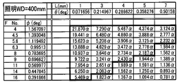
- the value of the angle of view ⁇ is shown, and the corresponding column of each table shows a value obtained by multiplying ⁇ / ⁇ by including the value of ⁇ of the first light source 20.
- the value ⁇ is approximately 1, the bright portion appears effectively under the condition that the value of ⁇ ⁇ ⁇ / ⁇ shown in FIG. It was confirmed to do.
- the bright portion appears effectively under the condition that ⁇ ⁇ ⁇ / ⁇ is larger than 2.
- the distance from the glass plate G to the surface of the imaging lens 23 of the first camera 22 was 380 mm.
- the illumination WD from the irradiation surface of the first linear light source 20 to the measurement position of the glass plate G is 200 mm in FIG. 5A and 400 mm in FIG. 5B.
- the area of the part where the circle of confusion is blocked by the optical path shielding member 24 is set to 50% of the area of the circle of confusion.
- the glass plate G is irradiated with the parallel light from an oblique direction, and defects that have been missed by the conventional automatic defect inspection similar to the schlieren imaging method can be extracted with high accuracy and cannot be repaired. This is effective in that the defects of the glass plate G can be distinguished. Thereby, the glass plate G can be cut out to a predetermined size so as to avoid a defective portion that cannot be repaired.
Landscapes
- Analytical Chemistry (AREA)
- Physics & Mathematics (AREA)
- Health & Medical Sciences (AREA)
- Life Sciences & Earth Sciences (AREA)
- Chemical & Material Sciences (AREA)
- Biochemistry (AREA)
- General Health & Medical Sciences (AREA)
- General Physics & Mathematics (AREA)
- Immunology (AREA)
- Pathology (AREA)
- Textile Engineering (AREA)
- Engineering & Computer Science (AREA)
- Investigating Materials By The Use Of Optical Means Adapted For Particular Applications (AREA)
Abstract
Description
ガラス板に含まれる泡や表面のキズ等の欠陥は、低減することが可能であるが、必ずしも完全に除去できるものではないため、検査工程で泡等の存在するガラス板の部分は除去する等の処置が必要である。このため、従来より、製造されたガラス板等の透明性を有する板状体に存在する泡等の欠陥を検査する装置が種々提案されている。
特に、第1のカメラの受光素子が、板状体を挟んで、第1の光源に正対するように第1のカメラを配置するのが好ましい。ここで正対するように配置するとは、前記第1のカメラの受光素子が、ガラス板Gを挟んで、第1の光源の最大光強度の方向に位置するように配置することをいう。
その際、前記処理装置は、板状体で反射した画像中の前記暗部の領域と、板状体の他方の面で反射した画像中の暗部との位置ずれに基づいて、板状体の厚さ方向の、欠陥の位置情報を求めることが好ましい。
ここで、前記第1の欠陥検査装置と前記第2の欠陥検査装置は、搬送方向において隣り合うようにして設けられることが好ましい。前記第1の欠陥検査装置と前記第2の欠陥検査装置との距離が短い方が、長い場合に比べて、欠陥の検出と特定を、より短い時間内で処理できることになるからである。
特に、照明発光有効角に対する画角の比率に第1の光源の発光指向性を表す値α(0以上1以下の数値)を乗算した値が、2より大きい第1の条件と、光路遮蔽部材により前記錯乱円が遮断される部分の面積が前記錯乱円の面積の43~57%になるように設定される第2の条件と、を満たすように第1のカメラの光学系を設定することにより、明視野画像に上記明部を有効に生じさせることができる。特に、計測に用いる第1の光源と第1のカメラとが、ガラス板Gを挟んで正対するように設けることで、より効果的に欠陥検査を行なうことができる。
また、板状体の面に照明光を照射する前記第2の光源と、照射され板状体の面で反射して得られる反射光を集光し、明視野反射画像を撮影する、板状体から見て前記第2の光源と同じ側に設けられる前記第2のカメラと、を有し、前記処理装置は、前記第2のカメラで撮影された明視野反射画像から、板状体の面で反射した画像中の暗部の領域を抽出し、この暗部の領域が前記明部の領域と近接して向かい合う場合、欠陥の実像と欠陥の鏡像との位置ずれに基づいて、板状体に位置する欠陥の厚さ方向の位置情報を求めることができる。
図1に示される欠陥検査システム10は、第1の欠陥検査装置12と、第2の欠陥検査装置14と、処理装置16と、を有して構成されている。
第1の欠陥検査装置12と第2の欠陥検査装置14は、ガラス板Gの搬送経路に沿って上流側から、この順に設けられる。処理装置16は、第1の欠陥検査装置12と第2の欠陥検査装置14で得られた画像を処理し、欠陥検出を行う装置である。
ガラス板Gは、溶融炉から取り出され所定の厚さとなった長尺状の板材であり、搬送経路に設けられた複数の駆動ローラ18上で搬送される。
具体的には、第1の欠陥検査装置12は、ガラス板Gの面に、駆動ローラ18の側(下側)から投光する第1の線状光源20と、ガラス板Gを通過した透過光を集光して明視野画像を撮影する第1のカメラ22と、第1の線状光源20の透過光の光路中の第1のカメラ22の前面の位置に設けられるナイフエッジ状の光路遮蔽部材24と、を有する。
第1のカメラ22は、ガラス板Gの面から、第1のカメラ22の結像レンズ23(図2参照)のピントが合う位置、例えば200~400mm離れた位置に受光面が来るように設けられる。第1のカメラ22には、結像レンズ23を備える光学系、及び、図示されないが、開口を調整する絞りを有する。第1のカメラ22で得られた画像データは、ライン状に読み取られる度に逐次処理装置16に送られる。
このような光路を遮断する範囲は、例えば、光遮蔽部材24とガラス板Gとの間の距離と、第1のカメラ22の絞り値とを調整することで実現できる。光路を遮断する範囲をこの範囲に設定することにより、後述するように、明視野画像内に存在する泡等の欠陥によってつくられる暗部の領域に近接して、明部の領域を効率よく形成させるためである。
ここで、第1の線状光源20の発光指向性を表す値αとは、図3に示すように、横軸に光源の照射面に直交する方向を方位角0度として方位角度をとり、縦軸に最大光強度の値を1としたときの、相対光強度の平均値をいう。
上記した第1の欠陥検査装置12による検出結果に加えて、この第2の欠陥検査装置14の検出結果を組み合わせて、総合的に評価することにより、ガラス板Gに存在する欠陥の特定をより的確に行うことができるようになった。
第1の欠陥検査装置12で得られる画像は、上述したように、明視野画像であり、ガラス板Gの欠陥は、欠陥領域の乱反射によって、画像中では暗部となって現れる。また、上述したように、第1のカメラ22の光学系の直前には、光路の一部分を遮断するナイフエッジ状の光路遮蔽部材24が設けられていることにより、この光路遮蔽部材24により、画像中の暗部の領域と近接して向かい合うように、あるいは接して対するように、明部の領域が形成される。この明部は、欠陥の部分の屈折異常により発生し、明視野画像の背景部分に比べて明度が高い。
このため、処理装置16では、明視野画像において、明視野画像における背景部分の画像データの値より高い閾値を設定し、この閾値以上の領域を明部の領域として抽出する。
なお、第1のカメラ22から送られてくる画像データは、検査位置を通過してラインセンサー型カメラで読み取られた一次元の画像データであるので、処理装置16では、複数ライン(例えば500ライン)の画像データが蓄積されて一定の面領域の画像が得られると、上記明部の領域の抽出を開始する。この抽出した明部の領域の位置情報は、ガラス板Gに存在する欠陥領域の検出の際に、以下のようにして用いられる。
暗部の領域の抽出には、予め設定された閾値を用いて行われる。
次に、この実像の中心位置と鏡像の中心位置との位置ずれ量を求め、この位置ずれ量に基づいて欠陥のガラス板Gにおける厚さ方向の位置を算出する。
また、処理装置16は、第2のカメラ30で得られた欠陥の実像を用いて暗部の領域の大きさを求め、この領域の大きさから、欠陥の大きさを推定する。なお、処理装置16は、上記明部の領域の情報に基づく処理と独立して、上記明部の領域の情報を用いることなく、予め設定された閾値を用いて暗部の領域を抽出する。
ガラス板Gの面上にある異物やキズ等の欠陥は、第1の欠陥検査装置12から得られる明視野画像中では明部を形成しない。
すなわち、図2に示す各部分の配置において、照明発光有効角θに対する画角φの比率に値αを乗算した値が、2より大きい第1の条件を満たすように、第1のカメラ22とガラス板Gとの間の距離、ガラス板Gと第1の線状光源20との間の距離、第1の線状光源の照射幅Lが設定されている。
また、光路遮蔽部材24の配置位置の、結像レンズ23の光軸に直交する面にできる、受光面からみた視野範囲の縁を定める錯乱円を定めたとき、光路遮蔽部材24により錯乱円が遮断される部分の面積が、錯乱円の面積の43~57%になる第2の条件を満たすように、第1のカメラ22の絞り値、および第1のカメラ22とガラス板Gとの間の距離が設定されている。
さらに、第1のカメラ22の受光素子が、ガラス板Gを挟んで、第1の線状光源20の最大光強度の方向に位置するように、第1のカメラ22が配置される。
この3つの条件を満たすように各装置を配置することで、明視野画像に上記明部を有効に生じさせることができる。
また、F値を小さくすることにより、撮影における被写体焦点深度は浅くなり、画像のピンボケが生じ易くなるといった不都合が生じる。このため、明部を効率よく抽出するためには、F5.6~F11が好ましく、第1のカメラ20の発光部分34の幅L1~20mmの範囲において、上記比率に値αを乗算した値が2より大きいことが好ましい。
なお、ガラス板Gと第1のカメラ22の結像レンズ23の表面までの距離を380mmとした。第1の線状光源20の照射面からガラス板Gの計測位置までの照明WDは、図5Aでは200mm、図5Bでは400mmである。このときの光路遮蔽部材24により錯乱円が遮断される部分の面積が、錯乱円の面積の50%になるようにした。
12 第1の欠陥検査装置
14 第2の欠陥検査装置
16 処理装置
18 駆動ローラ
20 第1の線状光源
22 第1のカメラ
23 結像レンズ
24 光路遮蔽部材
28 第2の光源
30 第2のカメラ
32 ディスプレイ
34 発光部分
Claims (6)
- 透明性を有する板状体に存在する欠陥を検出する欠陥検査システムであって、
前記板状体の面に投光する第1の光源と、
前記板状体を通過した透過光を集光して明視野画像を撮影する第1のカメラと、
前記第1のカメラの透過光の光路中の前記第1のカメラの前面の位置に設けられるナイフエッジ状の光路遮蔽部材と、を有する第1の欠陥検査装置と、
前記第1のカメラで撮影された明視野画像の中から、明視野画像の背景成分の信号値に比べて高い信号値を閾値として、明視野画像の中から明部の領域を探索し、探索の結果、明部の領域を抽出したとき、この明部の領域を用いて、前記板状体に欠陥領域が存在するか否かを判別する処理装置と、を備えることを特徴とする欠陥検査システム。 - 前記第1の光源は、線状光源であり、
前記第1のカメラの受光面の前面には、板状体の像を結像するための結像レンズが設けられ、
前記第1の光源から、前記結像レンズを介して前記第1のカメラの受光面に至る前記第1の光源の透過光の光束の拡がり角の半分の角度を照明発光有効角とし、前記第1のカメラの受光面の位置から前記結像レンズを介して前記第1の光源の照射面に至る視野範囲の見込み角の半分の角度を画角とし、前記第1の光源の発光指向性を表す値をαとしたとき、前記照明発光有効角に対する前記画角の比率に前記第1の光源の発光指向性を表す値αを乗算した値が、2より大きい第1の条件と、
前記光路遮蔽部材の前記透過光の通過位置において、前記結像レンズの光軸に直交する面にできる前記受光面からみた視野範囲である錯乱円を定めたとき、前記光路遮蔽部材により前記錯乱円が遮断される部分の面積が、前記錯乱円の面積の43~57%になる第2の条件と、を満たすように、前記第1の光源、前記結像レンズおよび前記第1のカメラが設定されている請求項1に記載の欠陥検査システム。 - 前記第1の欠陥検査装置の他に、前記第1の欠陥検査装置の検査対象とする板状体に対して、板状体から反射した照明光を受光して、欠陥を検査する第2の欠陥検査装置を有し、
前記第2の欠陥検査装置は、
板状体の面に照明光を照射する第2の光源と、
照射され板状体の面で反射して得られる反射光を集光し、明視野反射画像を撮影する、板状体から見て前記第2の光源と同じ側に設けられる第2のカメラと、を有し、
前記処理装置は、前記第2のカメラで撮影された明視野反射画像から、板状体で反射した画像中の暗部の領域を抽出し、この暗部の領域が前記明部の領域と近接して向かい合う場合、板状体に欠陥が存在すると判別する請求項1に記載の欠陥検査システム。 - 前記処理装置は、前記明視野反射画像に欠陥の像として形成される欠陥の実像と欠陥の鏡像との位置ずれに基づいて、板状体に位置する欠陥の厚さ方向の位置情報を求める請求項3に記載の欠陥検査システム。
- 前記板状体は、一方向に搬送されて移動し、
前記第1の欠陥検査装置と前記第2の欠陥検査装置は、前記第1の欠陥検査装置が、前記第2の欠陥検査装置の上流側に設けられている請求項1に記載の欠陥検査システム。 - 透明性を有する板状体に存在する欠陥を検出する欠陥検査方法であって、
第1の線状光源から前記板状体の面に投光し、前記板状体を通過した透過光を集光して第1のカメラで明視野画像を撮影するとき、
前記第1のカメラの透過光の光路中の前記第1のカメラの前面の位置にナイフエッジ状の光路遮蔽部材を設けて撮影し、
前記第1のカメラで撮影された明視野画像の中から、明視野画像の背景成分の信号値に比べて高い信号値を閾値として、明視野画像の中から明部の領域を探索し、探索の結果、明部の領域を抽出したとき、この明部の領域を用いて、前記板状体に欠陥領域が存在するか否かを判別することを特徴とする欠陥検査方法。
Priority Applications (1)
| Application Number | Priority Date | Filing Date | Title |
|---|---|---|---|
| CN2009801335442A CN102132148B (zh) | 2008-08-25 | 2009-07-28 | 缺陷检查系统及缺陷检查方法 |
Applications Claiming Priority (2)
| Application Number | Priority Date | Filing Date | Title |
|---|---|---|---|
| JP2008215091A JP2010048745A (ja) | 2008-08-25 | 2008-08-25 | 欠陥検査システムおよび欠陥検査方法 |
| JP2008-215091 | 2008-08-25 |
Publications (1)
| Publication Number | Publication Date |
|---|---|
| WO2010024082A1 true WO2010024082A1 (ja) | 2010-03-04 |
Family
ID=41721254
Family Applications (1)
| Application Number | Title | Priority Date | Filing Date |
|---|---|---|---|
| PCT/JP2009/063445 Ceased WO2010024082A1 (ja) | 2008-08-25 | 2009-07-28 | 欠陥検査システムおよび欠陥検査方法 |
Country Status (5)
| Country | Link |
|---|---|
| JP (1) | JP2010048745A (ja) |
| KR (1) | KR20110058784A (ja) |
| CN (1) | CN102132148B (ja) |
| TW (1) | TW201009324A (ja) |
| WO (1) | WO2010024082A1 (ja) |
Cited By (8)
| Publication number | Priority date | Publication date | Assignee | Title |
|---|---|---|---|---|
| WO2012093633A1 (ja) * | 2011-01-06 | 2012-07-12 | 日本電気硝子株式会社 | フラットパネルディスプレイ用のガラス基板の検査方法及びフラットパネルディスプレイ用のガラス基板 |
| CN105241891A (zh) * | 2015-08-27 | 2016-01-13 | 任红霞 | 一种基于wifi网络的玻璃缺陷检测方法 |
| EP3101167A3 (de) * | 2015-06-01 | 2017-01-04 | Herbert Kannegiesser GmbH | Verfahren zur prüfung gewaschener oder gereinigter wäschestücke |
| CN108267460A (zh) * | 2018-02-26 | 2018-07-10 | 湖南科创信息技术股份有限公司 | 用于透明材料缺陷检测的矩阵式视觉检测系统和方法 |
| CN108872246A (zh) * | 2018-05-29 | 2018-11-23 | 湖南科创信息技术股份有限公司 | 板面材料全视面缺陷检测系统 |
| CN109682836A (zh) * | 2019-01-29 | 2019-04-26 | 安徽利珀科技有限公司 | 一种缺陷检测装置 |
| TWI695164B (zh) * | 2017-11-29 | 2020-06-01 | 台灣積體電路製造股份有限公司 | 寬頻晶圓缺陷偵測系統及寬頻晶圓缺陷偵測方法 |
| CN115524341A (zh) * | 2022-01-07 | 2022-12-27 | 西安获德图像技术有限公司 | 一种玻璃纤维拉挤板外观质量检测系统及其检测方法 |
Families Citing this family (39)
| Publication number | Priority date | Publication date | Assignee | Title |
|---|---|---|---|---|
| KR101198406B1 (ko) | 2010-04-21 | 2012-11-07 | (주)에이앤아이 | 패턴 검사 장치 |
| JP5881278B2 (ja) | 2010-05-20 | 2016-03-09 | 株式会社プレックス | 布片検査装置および検査方法 |
| KR101745883B1 (ko) | 2011-03-16 | 2017-06-12 | 해성디에스 주식회사 | 인쇄회로기판의 광학 검사 장치 및 방법 |
| JP5935266B2 (ja) * | 2011-09-01 | 2016-06-15 | 東レ株式会社 | キズ欠点検査方法およびシートの製造方法 |
| CN103907013B (zh) * | 2011-11-09 | 2016-12-28 | 株式会社久保田 | 粒状体检查装置 |
| CN103175569B (zh) * | 2011-12-21 | 2015-07-15 | 北京兆维电子(集团)有限责任公司 | 单光源双相机的采集装置 |
| KR101409217B1 (ko) * | 2012-02-27 | 2014-06-20 | 엘아이지에이디피 주식회사 | 합착기판의 검사장치 및 검사방법 |
| JP5966704B2 (ja) * | 2012-07-11 | 2016-08-10 | 株式会社島津製作所 | 基板検査装置および基板検査装置用透過照明装置 |
| KR101387090B1 (ko) * | 2012-10-24 | 2014-04-21 | 길기재 | 투명체 표면 검사 장치 및 방법 |
| JP2014157086A (ja) * | 2013-02-15 | 2014-08-28 | Dainippon Screen Mfg Co Ltd | パターン検査装置 |
| CN103630544B (zh) * | 2013-11-07 | 2016-09-14 | 江苏大学 | 一种视觉在线检测系统 |
| JP6296499B2 (ja) * | 2014-08-11 | 2018-03-20 | 株式会社 東京ウエルズ | 透明基板の外観検査装置および外観検査方法 |
| CN106248684B (zh) * | 2015-06-03 | 2019-12-17 | 法国圣戈班玻璃公司 | 用于检测透明基底的内部瑕疵的光学装置及方法 |
| CN105091764A (zh) * | 2015-09-06 | 2015-11-25 | 苏州南光电子科技有限公司 | 基于激光和ccd的玻璃厚度测量系统的测量方法 |
| JP6642223B2 (ja) * | 2016-04-13 | 2020-02-05 | Agc株式会社 | 透明板表面検査装置、透明板表面検査方法、およびガラス板の製造方法 |
| FR3053792B1 (fr) * | 2016-07-06 | 2023-07-14 | Tiama | Procede, dispositif et ligne d'inspection pour la determination d'une bavure a l'endroit d'un bord interne d'une surface de bague |
| JP6405461B2 (ja) * | 2016-09-07 | 2018-10-17 | 株式会社Subaru | 損傷検知システム及び損傷検知方法 |
| JP6788837B2 (ja) * | 2017-01-06 | 2020-11-25 | 日本電気硝子株式会社 | ガラス板の検査方法及びその製造方法並びにガラス板の検査装置 |
| US10289930B2 (en) * | 2017-02-09 | 2019-05-14 | Glasstech, Inc. | System and associated for online measurement of the optical characteristics of a glass sheet |
| CN107014826A (zh) * | 2017-04-12 | 2017-08-04 | 武汉华星光电技术有限公司 | Cf基板微观检查机 |
| CN106932406A (zh) * | 2017-04-28 | 2017-07-07 | 许迪 | 一种检测透明物体缺陷的装置 |
| CN107247059B (zh) * | 2017-06-09 | 2020-05-01 | 华北电力大学(保定) | 基于空气热纹影分布的绝缘子故障检测装置及其方法 |
| EP3477248B1 (de) * | 2017-10-26 | 2023-06-07 | Heinrich Georg GmbH Maschinenfabrik | Inspektionssystem und verfahren zur fehleranalyse |
| CN108169240A (zh) * | 2017-12-28 | 2018-06-15 | 湖南文理学院 | 泡沫镍表面缺陷检测装置 |
| FR3076619B1 (fr) | 2018-01-05 | 2020-01-24 | Tiama | Procede, dispositif et ligne d'inspection pour determiner la geometrie tridimensionnelle d'une surface de bague de recipient |
| KR102030014B1 (ko) * | 2018-03-26 | 2019-11-08 | 제이티웨이 주식회사 | 렌즈 제조물 검사 시스템 및 렌즈 제조물 검사 방법 |
| KR102181637B1 (ko) * | 2018-05-24 | 2020-11-23 | (주)쎄미시스코 | 검사 대상물 에지 결함 검사 시스템 및 그 방법 |
| JP2020085587A (ja) * | 2018-11-21 | 2020-06-04 | 日本電気硝子株式会社 | ガラス板の製造方法、及びガラス板の製造装置 |
| CN112888531B (zh) * | 2018-12-11 | 2023-04-14 | 本田技研工业株式会社 | 工件检查装置和工件检查方法 |
| TWI699465B (zh) * | 2019-05-16 | 2020-07-21 | 亞亞科技股份有限公司 | 晶圓內外層取像裝置 |
| JP7220128B2 (ja) * | 2019-06-21 | 2023-02-09 | 東洋ガラス株式会社 | ガラスびんの検査方法及びガラスびんの製造方法 |
| JP2021004769A (ja) * | 2019-06-25 | 2021-01-14 | 住友金属鉱山株式会社 | 基板の検査装置、基板の検査方法 |
| KR102622753B1 (ko) | 2020-02-17 | 2024-01-10 | 삼성에스디아이 주식회사 | 이차전지용 레이저 용접 방법 및 모니터링 방법 |
| CN111351795A (zh) * | 2020-02-27 | 2020-06-30 | 杨孝兰 | 一种基于特殊结构光的镜面物体及透明物体检测方法 |
| JP2022020873A (ja) * | 2020-07-21 | 2022-02-02 | 三友工業株式会社 | 撮像装置及び撮像装置を有する表面検査装置、撮像方法及びプログラム |
| KR20230034023A (ko) | 2021-09-02 | 2023-03-09 | 박노진 | 광학 이미지 추출장치 및 광학 이미지 추출장치용 사선방향광학기기 그리고 광학 이미지 추출장치용 직선방향광학기기 |
| CN114660090B (zh) * | 2022-02-24 | 2025-09-30 | 彩虹显示器件股份有限公司 | 一种利用挡刀检测平板玻璃夹杂物缺陷变形的装置及方法 |
| CN115494065B (zh) * | 2022-04-28 | 2025-06-27 | 浙江大学台州研究院 | 一种基于正光图像的管材扩口的缺陷判断方法及其装置 |
| CN118425049B (zh) * | 2024-07-05 | 2024-11-29 | 宁德时代新能源科技股份有限公司 | 焊印检测系统和方法 |
Citations (3)
| Publication number | Priority date | Publication date | Assignee | Title |
|---|---|---|---|---|
| JPH09258197A (ja) * | 1996-03-18 | 1997-10-03 | Hitachi Electron Eng Co Ltd | ガラス基板の表裏欠陥識別方法 |
| JP2001141662A (ja) * | 1999-11-18 | 2001-05-25 | Central Glass Co Ltd | 透明板状体の欠点検出方法および検出装置 |
| JP2005069989A (ja) * | 2003-08-27 | 2005-03-17 | Apollo Mec:Kk | 検査装置 |
Family Cites Families (6)
| Publication number | Priority date | Publication date | Assignee | Title |
|---|---|---|---|---|
| JPH11316195A (ja) * | 1998-04-30 | 1999-11-16 | Asahi Glass Co Ltd | 透明板の表面欠陥検出装置 |
| WO2003005007A1 (en) * | 2001-07-05 | 2003-01-16 | Nippon Sheet Glass Co., Ltd. | Method and device for inspecting defect of sheet-shaped transparent body |
| JP2005049291A (ja) * | 2003-07-31 | 2005-02-24 | Nippon Sheet Glass Co Ltd | 透明板状体の集光作用を有する微小欠点を検出する装置および方法 |
| WO2006057125A1 (ja) * | 2004-11-24 | 2006-06-01 | Asahi Glass Company, Limited | 透明板状体の欠陥検査方法および装置 |
| KR20070121820A (ko) * | 2005-04-06 | 2007-12-27 | 코닝 인코포레이티드 | 유리 검사 시스템 및 이를 이용한 유리 검사 방법 |
| JP4679282B2 (ja) * | 2005-07-19 | 2011-04-27 | 株式会社日立ハイテクノロジーズ | 基板検査装置及び基板検査方法 |
-
2008
- 2008-08-25 JP JP2008215091A patent/JP2010048745A/ja not_active Withdrawn
-
2009
- 2009-07-28 CN CN2009801335442A patent/CN102132148B/zh active Active
- 2009-07-28 WO PCT/JP2009/063445 patent/WO2010024082A1/ja not_active Ceased
- 2009-07-28 KR KR1020117004448A patent/KR20110058784A/ko not_active Withdrawn
- 2009-07-31 TW TW098125949A patent/TW201009324A/zh unknown
Patent Citations (3)
| Publication number | Priority date | Publication date | Assignee | Title |
|---|---|---|---|---|
| JPH09258197A (ja) * | 1996-03-18 | 1997-10-03 | Hitachi Electron Eng Co Ltd | ガラス基板の表裏欠陥識別方法 |
| JP2001141662A (ja) * | 1999-11-18 | 2001-05-25 | Central Glass Co Ltd | 透明板状体の欠点検出方法および検出装置 |
| JP2005069989A (ja) * | 2003-08-27 | 2005-03-17 | Apollo Mec:Kk | 検査装置 |
Cited By (8)
| Publication number | Priority date | Publication date | Assignee | Title |
|---|---|---|---|---|
| WO2012093633A1 (ja) * | 2011-01-06 | 2012-07-12 | 日本電気硝子株式会社 | フラットパネルディスプレイ用のガラス基板の検査方法及びフラットパネルディスプレイ用のガラス基板 |
| EP3101167A3 (de) * | 2015-06-01 | 2017-01-04 | Herbert Kannegiesser GmbH | Verfahren zur prüfung gewaschener oder gereinigter wäschestücke |
| CN105241891A (zh) * | 2015-08-27 | 2016-01-13 | 任红霞 | 一种基于wifi网络的玻璃缺陷检测方法 |
| TWI695164B (zh) * | 2017-11-29 | 2020-06-01 | 台灣積體電路製造股份有限公司 | 寬頻晶圓缺陷偵測系統及寬頻晶圓缺陷偵測方法 |
| CN108267460A (zh) * | 2018-02-26 | 2018-07-10 | 湖南科创信息技术股份有限公司 | 用于透明材料缺陷检测的矩阵式视觉检测系统和方法 |
| CN108872246A (zh) * | 2018-05-29 | 2018-11-23 | 湖南科创信息技术股份有限公司 | 板面材料全视面缺陷检测系统 |
| CN109682836A (zh) * | 2019-01-29 | 2019-04-26 | 安徽利珀科技有限公司 | 一种缺陷检测装置 |
| CN115524341A (zh) * | 2022-01-07 | 2022-12-27 | 西安获德图像技术有限公司 | 一种玻璃纤维拉挤板外观质量检测系统及其检测方法 |
Also Published As
| Publication number | Publication date |
|---|---|
| TW201009324A (en) | 2010-03-01 |
| JP2010048745A (ja) | 2010-03-04 |
| CN102132148B (zh) | 2012-12-12 |
| KR20110058784A (ko) | 2011-06-01 |
| CN102132148A (zh) | 2011-07-20 |
Similar Documents
| Publication | Publication Date | Title |
|---|---|---|
| JP2010048745A (ja) | 欠陥検査システムおよび欠陥検査方法 | |
| CN102954970B (zh) | 用于检测玻璃衬底的表面缺陷的设备 | |
| JP5909751B2 (ja) | 平板ガラスの異物検査装置及び検査方法 | |
| EP1816466B1 (en) | Method and device for inspecting defect of transparent plate body | |
| CN101611309B (zh) | 用于照明材料以进行自动化检测的方法和设备 | |
| KR101326455B1 (ko) | 투명 기판에서의 결함을 특성화하기 위한 장치 및 방법 | |
| CN101449151B (zh) | 对玻璃窗的检验 | |
| JP5348765B2 (ja) | 平板状透明体の微小凹凸欠陥検査方法及び装置 | |
| TWI412736B (zh) | 基板內部缺陷檢查裝置及方法 | |
| CN102023164A (zh) | 用于检测透明平板的局部缺陷的装置和方法 | |
| CN106996937B (zh) | 一种玻璃基板内缺陷检测方法及装置 | |
| JP4362335B2 (ja) | 検査装置 | |
| JP2006071284A (ja) | ガラス基板欠陥の表裏識別方法 | |
| KR101860733B1 (ko) | 필름 검사 장치 및 필름 검사 방법 | |
| US11249032B2 (en) | Methods and apparatus for detecting surface defects on glass sheets | |
| JP2006292412A (ja) | 表面検査装置、表面検査方法、及び基板の製造方法 | |
| TWI819285B (zh) | 透射光學系統的檢查裝置 | |
| KR101103347B1 (ko) | 평판 유리 표면 이물질 검사 장치 | |
| JP2010054273A (ja) | 欠陥検出装置及び欠陥検出方法 | |
| JP5647716B2 (ja) | 微小凹凸欠陥検査機用の簡易テレセントリックレンズ装置 | |
| JP7827255B2 (ja) | 透明物体の表面を検査する装置および対応方法 | |
| JP2016099314A (ja) | 検査システムおよび検査方法 | |
| KR20220112567A (ko) | 결함 검사 장치 | |
| JP2007024733A (ja) | 基板検査装置及び基板検査方法 | |
| JP2022090247A (ja) | 光学フィルムの縁部検出方法 |
Legal Events
| Date | Code | Title | Description |
|---|---|---|---|
| WWE | Wipo information: entry into national phase |
Ref document number: 200980133544.2 Country of ref document: CN |
|
| 121 | Ep: the epo has been informed by wipo that ep was designated in this application |
Ref document number: 09809736 Country of ref document: EP Kind code of ref document: A1 |
|
| ENP | Entry into the national phase |
Ref document number: 20117004448 Country of ref document: KR Kind code of ref document: A |
|
| NENP | Non-entry into the national phase |
Ref country code: DE |
|
| 122 | Ep: pct application non-entry in european phase |
Ref document number: 09809736 Country of ref document: EP Kind code of ref document: A1 |