WO2010023987A1 - 有機elデバイスおよびその製造方法 - Google Patents
有機elデバイスおよびその製造方法 Download PDFInfo
- Publication number
- WO2010023987A1 WO2010023987A1 PCT/JP2009/057073 JP2009057073W WO2010023987A1 WO 2010023987 A1 WO2010023987 A1 WO 2010023987A1 JP 2009057073 W JP2009057073 W JP 2009057073W WO 2010023987 A1 WO2010023987 A1 WO 2010023987A1
- Authority
- WO
- WIPO (PCT)
- Prior art keywords
- organic
- layer
- film
- substrate
- bond
- Prior art date
- Legal status (The legal status is an assumption and is not a legal conclusion. Google has not performed a legal analysis and makes no representation as to the accuracy of the status listed.)
- Ceased
Links
Images

Classifications
-
- H—ELECTRICITY
- H05—ELECTRIC TECHNIQUES NOT OTHERWISE PROVIDED FOR
- H05B—ELECTRIC HEATING; ELECTRIC LIGHT SOURCES NOT OTHERWISE PROVIDED FOR; CIRCUIT ARRANGEMENTS FOR ELECTRIC LIGHT SOURCES, IN GENERAL
- H05B33/00—Electroluminescent light sources
- H05B33/02—Details
- H05B33/04—Sealing arrangements, e.g. against humidity
-
- H—ELECTRICITY
- H10—SEMICONDUCTOR DEVICES; ELECTRIC SOLID-STATE DEVICES NOT OTHERWISE PROVIDED FOR
- H10K—ORGANIC ELECTRIC SOLID-STATE DEVICES
- H10K59/00—Integrated devices, or assemblies of multiple devices, comprising at least one organic light-emitting element covered by group H10K50/00
- H10K59/80—Constructional details
- H10K59/87—Passivation; Containers; Encapsulations
- H10K59/873—Encapsulations
-
- H—ELECTRICITY
- H10—SEMICONDUCTOR DEVICES; ELECTRIC SOLID-STATE DEVICES NOT OTHERWISE PROVIDED FOR
- H10K—ORGANIC ELECTRIC SOLID-STATE DEVICES
- H10K50/00—Organic light-emitting devices
- H10K50/80—Constructional details
- H10K50/84—Passivation; Containers; Encapsulations
- H10K50/841—Self-supporting sealing arrangements
-
- H—ELECTRICITY
- H10—SEMICONDUCTOR DEVICES; ELECTRIC SOLID-STATE DEVICES NOT OTHERWISE PROVIDED FOR
- H10K—ORGANIC ELECTRIC SOLID-STATE DEVICES
- H10K50/00—Organic light-emitting devices
- H10K50/80—Constructional details
- H10K50/84—Passivation; Containers; Encapsulations
- H10K50/844—Encapsulations
-
- H—ELECTRICITY
- H10—SEMICONDUCTOR DEVICES; ELECTRIC SOLID-STATE DEVICES NOT OTHERWISE PROVIDED FOR
- H10K—ORGANIC ELECTRIC SOLID-STATE DEVICES
- H10K59/00—Integrated devices, or assemblies of multiple devices, comprising at least one organic light-emitting element covered by group H10K50/00
- H10K59/80—Constructional details
- H10K59/87—Passivation; Containers; Encapsulations
- H10K59/871—Self-supporting sealing arrangements
-
- H—ELECTRICITY
- H10—SEMICONDUCTOR DEVICES; ELECTRIC SOLID-STATE DEVICES NOT OTHERWISE PROVIDED FOR
- H10K—ORGANIC ELECTRIC SOLID-STATE DEVICES
- H10K2102/00—Constructional details relating to the organic devices covered by this subclass
- H10K2102/301—Details of OLEDs
-
- H—ELECTRICITY
- H10—SEMICONDUCTOR DEVICES; ELECTRIC SOLID-STATE DEVICES NOT OTHERWISE PROVIDED FOR
- H10K—ORGANIC ELECTRIC SOLID-STATE DEVICES
- H10K2102/00—Constructional details relating to the organic devices covered by this subclass
- H10K2102/301—Details of OLEDs
- H10K2102/302—Details of OLEDs of OLED structures
- H10K2102/3023—Direction of light emission
- H10K2102/3026—Top emission
-
- H—ELECTRICITY
- H10—SEMICONDUCTOR DEVICES; ELECTRIC SOLID-STATE DEVICES NOT OTHERWISE PROVIDED FOR
- H10K—ORGANIC ELECTRIC SOLID-STATE DEVICES
- H10K71/00—Manufacture or treatment specially adapted for the organic devices covered by this subclass
- H10K71/40—Thermal treatment, e.g. annealing in the presence of a solvent vapour
Definitions
- the present invention relates to an organic EL device useful for display applications and a method for producing the same. More specifically, the present invention relates to an organic EL device that prevents moisture from entering from the outside environment and exhibits excellent luminous efficiency over a long period of time, and a method for manufacturing the same.
- organic EL devices using self-luminous organic EL elements have been actively studied for display applications.
- the organic EL device is expected to realize high light emission luminance and light emission efficiency. This is because a high current density can be realized at a low voltage.
- the practical application of high-definition multicolor light-emitting organic EL devices capable of multicolor display, particularly full color display is expected in the technical field of displays.
- the multicolor organic EL device has a defect that the light emission characteristic (current-luminance characteristic) is remarkably lowered by driving for a certain period.
- a typical cause of the deterioration of the light emission characteristics is the growth of dark spots. “Dark spot” means a light emitting defect point. This dark spot is considered to be generated by the oxidation or aggregation of the material of the constituent layer of the organic EL element during driving and storage due to oxygen or moisture in the element. The growth of dark spots proceeds not only during energization but also during storage.
- dark spot growth is (1) accelerated by oxygen or moisture present in the external environment surrounding the device, (2) affected by oxygen or moisture present as an adsorbate in the constituent layers, and (3) It is considered that it is affected by moisture adsorbed on components used for device manufacture or moisture intrusion during manufacture. As the growth continues, dark spots spread over the entire light emitting surface of the organic EL device.
- Patent Document 1 As a sealing thin film applicable to an organic EL device, a film mainly composed of silicon and silicon nitride formed by a plasma CVD method is used. Proposed. In Patent Document 1, this film is excellent because the number of silicon bonded to silicon relative to the number of silicon bonded to nitrogen measured by X-ray photoelectron spectroscopy is 0.6 or more and 2.0 or less. It is disclosed that sealing properties are exhibited.
- the organic EL device of the present invention includes a substrate and an organic EL element formed on the substrate, and the organic EL element includes a lower electrode, an organic EL layer, an upper electrode, and a protective layer.
- a silicon oxynitride film containing hydrogen, and the peak area ratio of the stretching mode determined by infrared absorption spectrum measurement is the absorption area of NH bonds to Si—N bonds in the silicon oxynitride film containing hydrogen The ratio is greater than 0.05 and less than or equal to 0.07, and the absorption area ratio of Si—H bonds to Si—N bonds is less than or equal to 0.15.
- the organic EL device of the present invention may have a structure in which the protective layer is in contact with the substrate and the lower electrode.
- the organic EL device of the present invention may have a structure in which the protective layer is in contact with the upper electrode and the lower electrode is in contact with the substrate. Moreover, it is desirable that the stress of each of the one or more inorganic films constituting the protective layer has an absolute value smaller than 20 MPa.
- the absorption areas of the N—H bond, Si—H bond, and Si—N bond in the present invention are as follows: (a) a step of measuring the infrared absorption spectrum of the silicon oxynitride film with the wave number as the horizontal axis; Correcting for subtracting the baseline from the obtained infrared absorption spectrum, (c) separating the peaks of the N—H, Si—H, and Si—N bonds using a Gaussian function, and (D) It can obtain
- the absorption area of the N-H bonds is determined from peaks present in 3250 ⁇ 3400 cm -1
- the absorption area of the Si-H bonds is determined from peaks present in 2100 ⁇ 2200 cm -1
- the absorption area of the Si—N bond can be obtained from the peak existing at 830 to 870 cm ⁇ 1 .
- the method for producing an organic EL device of the present invention includes (1) a step of preparing a substrate; (2) a step of forming an organic EL element comprising a lower electrode, an organic EL layer, an upper electrode and a protective layer,
- the protective layer is composed of one or more inorganic films, and at least one of the one or more inorganic films is a silicon oxynitride film containing hydrogen, and has a stretching mode required by infrared absorption spectrum measurement.
- the peak area ratio is such that the absorption area ratio of the NH bond to the Si—N bond in the silicon oxynitride film containing hydrogen is greater than 0.05 and less than or equal to 0.07.
- silicon oxynitride film containing hydrogen is monosilane, ammonia, N 2 O
- silicon oxynitride film containing hydrogen is monosilane, ammonia, N 2 O
- the flow rate ratio of ammonia to monosilane 0.5 or more and 1 or less, N 2 for monosilane is larger than 0 and smaller than 0.2.
- the present invention can maintain excellent luminous efficiency over a long period of time by using a protective layer having excellent moisture resistance.
- An organic EL device can be provided.
- the protective layer of the present invention has a high visible light transmittance, the configuration of the present invention is particularly effective in a top emission type organic EL device.
- FIG. 3 is a diagram showing an IR spectrum for determining a ratio of Si—N bonds, Si—H bonds and N—H bonds in a silicon oxynitride film.
- FIG. 3 is a diagram showing an IR spectrum subjected to peak separation in order to determine a ratio of Si—N bond, Si—H bond and N—H bond in a silicon oxynitride film.
- the organic EL device of the present invention includes a substrate and an organic EL element formed on the substrate, and the organic EL element includes a lower electrode, an organic EL layer, an upper electrode, and a protective layer.
- a silicon oxynitride film containing hydrogen, and the peak area ratio of the stretching mode determined by infrared absorption spectrum measurement is the absorption area of NH bonds to Si—N bonds in the silicon oxynitride film containing hydrogen The ratio is greater than 0.05 and less than or equal to 0.07, and the absorption area ratio of Si—H bonds to Si—N bonds is less than or equal to 0.15.
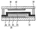
- FIG. 1 shows one example of the organic EL device of the present invention.
- the organic EL device of FIG. 1 is a top emission type organic EL device.
- the organic EL device includes a substrate 10, and a lower electrode 21, an organic EL layer 22, an upper electrode 23, and a protective layer 24 stacked in this order on the substrate 10.
- EL element 20 is included.
- the sealing substrate 30 on which the color conversion filter layer 40 is placed is bonded to the side of the substrate 10 on which the organic EL element 20 is formed with an adhesive layer 50. .
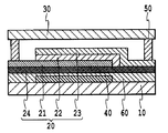
- FIG. 2 shows another example of the organic EL device of the present invention.
- the protective layer 24 is located between the substrate 10 and the lower electrode 21.
- the organic EL device in FIG. 2 is a bottom emission type organic EL device.
- FIG. 2 shows an example in which a color conversion filter layer 40 and a planarization layer 60 which are optional elements are further included between the substrate 10 and the protective layer 24.
- the substrate 10 of the present invention can be formed using any material that can withstand various conditions (for example, the solvent used, temperature, etc.) used to form other constituent layers.
- the substrate 10 desirably has excellent dimensional stability.
- the transparent material used to form the substrate 10 includes glass or acrylic resins such as polyolefin and polymethyl methacrylate, polyester resins such as polyethylene terephthalate, polycarbonate resins, and resins such as polyimide resins.
- the substrate 10 may be rigid or flexible.
- the substrate 10 may be formed using an opaque material such as silicon or ceramic. It can be formed using a flat material having insulation and rigidity capable of maintaining the form of the organic EL light emitting element.
- the substrate 10 may further include a plurality of switching elements (such as TFTs) and wiring on the surface thereof.
- This configuration is effective for manufacturing an active matrix driving type organic EL device having a plurality of independent light emitting portions.
- the lower electrode 21 positioned between the substrate 10 and the organic EL layer 22 and the upper electrode 23 positioned on the opposite side of the organic EL layer 22 from the substrate 10 are carriers injected into the organic EL layer 22 and an external drive circuit. It has the function of connection.
- the lower electrode 21 and the upper electrode 23 may be either an anode (hole injection electrode) or a cathode (electron injection electrode), respectively. However, one of the lower electrode 21 and the upper electrode 23 is an anode, and the other is a cathode.
- the lower electrode 21 and the upper electrode 23 may be a reflective electrode or a transparent electrode, provided that one of them is a transparent electrode.
- the lower electrode 21 is preferably a reflective electrode
- the upper electrode 23 is a transparent electrode.
- the upper electrode 23 is preferably a reflective electrode
- the lower electrode 21 is a transparent electrode.
- the reflective electrode used as the lower electrode 21 or the upper electrode 23 is a highly reflective metal (aluminum, silver, molybdenum, tungsten, nickel, chromium, etc.) or an alloy thereof, or an amorphous alloy (NiP, NiB, CrP, or CrB). Etc.).
- a particularly preferable material includes a silver alloy.
- the silver alloy that can be used is an alloy of silver and at least one metal selected from the group consisting of Group 10 nickel or platinum, Group 1 rubidium, and Group 14 lead, or silver. And an alloy with at least one metal selected from the group consisting of Group 2 magnesium and calcium.
- the transparent electrode used as the lower electrode 21 or the upper electrode 23 is made of conductive metal oxide such as SnO 2 , In 2 O 3 , In—Sn oxide, In—Zn oxide, ZnO, or Zn—Al oxide. Can be formed.
- the transparent electrode serves as a path for extracting light emitted from the organic EL layer 22 to the outside. Therefore, the transparent electrode desirably has a transmittance of 50% or more, preferably 85% or more within a wavelength range of 400 to 800 nm.
- the lower electrode 21 and the upper electrode 23 can be formed using a resistance heating method or an electron beam heating method vapor deposition method, or a sputtering method.
- a vapor deposition method film formation can be performed at a film formation speed of 0.1 to 10 nm / second at a pressure of 1.0 ⁇ 10 ⁇ 4 Pa or less.
- an inert gas such as Ar can be used as a sputtering gas, and film formation can be performed at a pressure of about 0.1 to 2.0 Pa.
- the upper electrode 23 is formed by sputtering, it is preferable not to directly irradiate the organic EL layer 22 with plasma formed in the vicinity of the target in order to prevent the deterioration of the organic EL layer 22 that becomes the surface of the deposition target substrate.
- the organic EL layer 22 is located between the lower electrode 21 and the upper electrode 23 and is in contact with each electrode. This is the core layer of the light emitting part.
- the organic EL layer 22 includes at least a light emitting layer, and includes a hole transport layer, a hole injection layer, an electron transport layer, and / or an electron injection layer as necessary.
- the organic EL layer 22 can have the following layer configuration.
- anode / light emitting layer / cathode (2) Anode / hole injection layer / light emitting layer / cathode (3) Anode / light emitting layer / electron injection layer / cathode (4) Anode / hole injection layer / light emitting layer / electron Injection layer / cathode (5) Anode / hole transport layer / light emitting layer / electron injection layer / cathode (6) Anode / hole injection layer / hole transport layer / light emitting layer / electron injection layer / cathode (7) Anode / Hole injection layer / hole transport layer / light-emitting layer / electron transport layer / electron injection layer / cathode In each of the above configurations (1) to (7), the anode and the cathode are the lower electrode 21 or the upper electrode 23, respectively. One of them.
- the light emitting layer can be formed using a known material.
- Materials for obtaining blue to blue-green light emission are, for example, fluorescent brighteners such as benzothiazole compounds, benzimidazole compounds or benzoxazole compounds; tris (8-hydroxyquinolinato) aluminum complex (Alq 3 ) Metal chelated oxonium compounds such as aluminum complexes represented by); styrylbenzene compounds such as 4,4′-bis (diphenylvinyl) biphenyl (DPVBi); aromatic dimethylidin compounds; condensed aromatic ring compounds; An aggregate compound; and a porphyrin-based compound.
- fluorescent brighteners such as benzothiazole compounds, benzimidazole compounds or benzoxazole compounds
- Alq 3 8-hydroxyquinolinato aluminum complex
- Metal chelated oxonium compounds such as aluminum complexes represented by
- styrylbenzene compounds such as 4,4′-bis (diphenylvinyl) biphenyl
- a light emitting layer that emits light in various wavelength ranges can be formed by adding a dopant to the host compound.
- a distyrylarylene compound, N, N′-ditolyl-N, N′-diphenylbiphenylamine (TPD), Alq 3 or the like can be used as the host compound.
- perylene blue purple
- coumarin 6 blue
- quinacridone compounds blue green to green
- rubrene yellow
- 4-dicyanomethylene-2- (p-dimethylaminostyryl) -6- Methyl-4H-pyran DCM, red
- platinum octaethylporphyrin complex PtOEP, red
- the hole transport layer can be formed using a material having a triarylamine partial structure, a carbazole partial structure, or an oxadiazole partial structure.
- Preferred materials for the hole transport layer are TPD, 4,4′-bis [N- (1-naphthyl) -N-phenylamino] biphenyl ( ⁇ -NPD), MTDAPB (o-, m-, p-). , M-MTDATA and the like.
- the hole injection layer can be formed using a material such as phthalocyanine (Pc) containing copper phthalocyanine complex (CuPc) or an indanthrene compound.
- the electron transport layer aluminum complexes such as Alq 3, oxadiazole derivatives such as PBD or TPOB, triazole derivatives such as TAZ, triazine derivatives, phenylquinoxalines acids, materials such as thiophene derivatives such as BMB-2T Can be formed.
- the electron injection layer can be formed using a material such as an aluminum complex such as Alq 3 or an aluminum quinolinol complex doped with an alkali metal or an alkaline earth metal.
- a buffer layer for further enhancing the carrier injection efficiency is optionally provided between the organic EL layer 22 and either the lower electrode 21 or the upper electrode 23 used as the cathode. It can also be formed selectively (not shown).
- the buffer layer can be formed using an electron injecting material such as an alkali metal, an alkaline earth metal or an alloy thereof, a rare earth metal, or a fluoride of the metal.
- each layer constituting the organic EL layer 22 has a film thickness sufficient to realize desired characteristics.
- the light emitting layer, the hole transport layer, the electron transport layer and the electron injection layer have a thickness of 2 to 50 nm, and the hole injection layer has a thickness of 2 to 200 nm.
- the optional buffer layer preferably has a thickness of 10 nm or less from the viewpoint of reducing driving voltage and improving transparency.
- Each component layer, buffer layer, and damage mitigating layer of the organic EL layer 22 can be produced using any means known in the art such as vapor deposition (resistance heating vapor deposition or electron beam heat vapor deposition).
- the protective layer 24 is a layer for preventing moisture from entering the electrode and / or the organic EL layer 22 from an external environment or a layer that may contain moisture.
- the protective layer 24 is a silicon oxynitride (SiON: H) film containing hydrogen.
- SiON silicon oxynitride
- the added film be a Si-based film in consideration of the ease of film formation.
- the protective layer 24 may be provided on the upper electrode 23 as shown in FIG. 1, or may be provided between the substrate 10 and the lower electrode 21 as shown in FIG. If necessary, a protective layer 24 may be provided on both the upper electrode 23 and between the substrate 10 and the lower electrode 21.
- the inorganic film constituting the protective layer 24 desirably has a small stress in order to prevent film peeling. In the present invention, it is desirable that the stress of the inorganic film has an absolute value of 20 MPa or less, whether it is shrinkable or extensible. The stress can be obtained from, for example, the amount of change in warpage of the Si wafer before and after forming the inorganic film after forming the inorganic film on the Si wafer.
- the protective layer 24 When the protective layer 24 is located on the emission path of light from the organic EL layer to the outside, it is desirable that the protective layer 24 has a high visible light transmittance. Specifically, it is desirable to have a transmittance of 50% or more, preferably 85% or more within a wavelength range of 400 to 800 nm. In addition, the protective layer 24 is desired to have excellent moisture resistance.
- the inventor of the present invention has an absorption area ratio of NH bonds to Si—N bonds (hereinafter referred to as NH / Si—N area ratio) of more than 0.05 and not more than 0.07, and Si—N—
- NH / Si—N area ratio an absorption area ratio of NH bonds to Si—N bonds
- Si—N— an absorption area ratio of Si—H bonds to N bonds
- the SiON: H film constituting the protective layer 24 can be formed using a chemical vapor deposition (CVD) method.
- CVD chemical vapor deposition
- a plasma CVD method in which high-frequency power is applied is desirable.
- a mixture of monosilane, ammonia, N 2 O and an inert gas can be used as a source gas.
- a mixed gas of monosilane, ammonia, N 2 O and nitrogen in order to realize the high visible light transmittance of the SiON: H film, it is desirable that the flow rate ratio of ammonia to monosilane is 0.5 or more.
- the flow rate ratio of ammonia to monosilane in order to realize the excellent moisture resistance of the SiON: H film, the flow rate ratio of ammonia to monosilane is 1 or less, and the flow rate ratio of N 2 O to monosilane is greater than 0 and less than 0.2. Is desirable.
- the absolute stress of the SiON: H film obtained is absolute.
- the value can be 20 MPa or less.
- the aforementioned flow rate ratio is also effective in satisfying the requirements of the N—H / Si—N area ratio and the Si—H / Si—N area ratio.
- the IR spectrum of the SiON: H film is measured.
- the IR spectrum in the present invention uses stretching mode absorption. This mode of absorption is preferred because of its high intensity and easy peak separation. Further, the spectrum is expressed using a linear axis of wave number (unit: cm ⁇ 1 ) as the horizontal axis, and has no partial expansion.
- IR spectra of the deposition target substrate on which the SiON: H film is formed and the deposition target substrate on which the SiON: H film is not formed are measured, and the difference spectrum is obtained. It is desirable to take.
- the obtained IR spectrum includes a change in absorbance due to light interference in the film.
- correction using a baseline is performed.
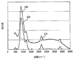
- FIG. 3 is a diagram for explaining this correction process, and shows the IR spectrum 100, the baseline 110, and the IR spectrum 120 after the baseline correction as measured.
- the baseline for the SiN: H film in the present invention is obtained by connecting the absorbance of the IR spectrum 100 at a wave number defined below with a straight line.
- the absorbance of the baseline 110 is subtracted from the absorbance of the IR spectrum 100 to obtain the IR spectrum 120 after baseline correction.
- peak separation is performed on the IR spectrum 120 after baseline correction. The peak separation is performed by expressing each peak with a Gaussian function G n represented by the formula (I).
- An is the maximum value of the absorbance of each peak
- C n is the wave number (unit: cm ⁇ 1 ) at which the absorbance of each peak is maximum
- x is the wave number
- B n is a variable.
- Bn regarding each peak is calculated
- FIG. 4 shows the result of peak separation of the IR spectrum 120 after baseline correction in FIG.
- a peak with a maximum at 830 ⁇ 870 cm -1 and a peak showing the stretching modes of Si-N bond an stretching modes of Si-H bonds a peak with a maximum at 2100 ⁇ 220 cm -1
- a peak having a maximum at 3250 to 3400 cm ⁇ 1 is regarded as a peak exhibiting an N—H bond stretching mode.
- the peak having a maximum at about 1200 cm ⁇ 1 is derived from the N—H bond, but is not used in the calculation of the N—H / Si—N area ratio of the present invention.
- the sealing substrate 30 is formed using, for example, glass; a metal such as SUS or Al; or an acrylic resin such as polyolefin or polymethyl methacrylate, a polyester resin such as polyethylene terephthalate, a polycarbonate resin, or a resin such as a polyimide resin. can do. When resin is used, the sealing substrate 30 may be rigid or flexible. In the top emission type structure as shown in FIG. 1, since the sealing substrate 30 hits a path for emitting light emitted from the organic EL layer 22 to the outside, the sealing substrate is made of a transparent material such as glass or resin. It is desirable to form 30.
- the color conversion filter layer 40 is a layer for adjusting the hue of light emitted from the organic EL layer 22.
- the “color conversion filter layer” in the present invention is a general term for a color filter layer, a color conversion layer, and a laminate of a color filter layer and a color conversion layer.
- the color conversion filter layer 40 may be provided inside the sealing substrate 30 as shown in FIG. 1, or may be provided between the substrate 10 and the lower electrode 21 as shown in FIG.
- the color conversion filter layer 40 is difficult to dry completely in order to protect the pigment contained therein, and may contain moisture. Therefore, as shown in FIG. 1, when the color conversion filter layer 40 is provided inside the sealing substrate, it is preferable to provide the protective layer 24 on the upper surface of the upper electrode 23. Similarly, as shown in FIG. 2, when the color conversion filter layer 40 is provided between the substrate 10 and the lower electrode 21, it is preferable to provide the protective layer 24 between the color conversion filter layer 40 and the lower electrode 21. .
- the color filter layer is a layer that transmits light in a specific wavelength range.
- the color filter layer has a function of improving the color purity of light from the organic EL layer 22 or the color conversion layer.
- the color filter layer can be formed using a commercially available color filter material for a flat panel display (for example, a color mosaic manufactured by FUJIFILM Electronics Materials Co., Ltd.).
- a coating method such as spin coating, roll coating, casting or dip coating can be used.
- a film formed by a coating method may be patterned by a photolithographic method or the like to form a color filter layer having a desired pattern.
- the color conversion layer is a layer that absorbs light in a specific wavelength range, performs wavelength distribution conversion, and emits light in a different wavelength range.
- the color conversion layer includes at least a fluorescent dye, and may include a matrix resin as necessary.
- the fluorescent dye absorbs light from the organic EL layer 22 and emits light in a desired wavelength region (for example, a red region, a green region, or a blue region).
- a desired wavelength region for example, a red region, a green region, or a blue region.
- rhodamine B, rhodamine 6G, rhodamine 3B, rhodamine 101, rhodamine 110, sulforhodamine, basic violet 11, and basic red 2 are fluorescent dyes that absorb light in the blue to blue-green region and emit fluorescence in the red region.
- Rhodamine dyes such as: cyanine dyes; pyridine dyes such as 1-ethyl-2- [4- (p-dimethylaminophenyl) -1,3-butadienyl] -pyridinium-perchlorate (pyridine 1); and oxazines System pigments.
- cyanine dyes such as 1-ethyl-2- [4- (p-dimethylaminophenyl) -1,3-butadienyl] -pyridinium-perchlorate (pyridine 1); and oxazines System pigments.
- various dyes having fluorescence as described above direct dyes, acid dyes, basic dyes, disperse dyes, etc. may be used.
- Fluorescent dyes that absorb light in the blue to blue-green region and emit fluorescence in the green region include, for example, 3- (2′-benzothiazolyl) -7-diethylaminocoumarin (coumarin 6), 3- (2′-benzimidazolyl) ) -7-diethylaminocoumarin (coumarin 7), 3- (2′-N-methylbenzimidazolyl) -7-diethylaminocoumarin (coumarin 30), 2,3,5,6-1H, 4H-tetrahydro-8-trifluoro Coumarin dyes such as methylquinolidine (9,9a, 1-gh) coumarin (coumarin 153); naphthalimide dyes such as Solvent Yellow 11 and Solvent Yellow 116; and Coumarin dyes such as Basic Yellow 51 Including.
- various dyes having fluorescence as described above direct dyes, acid dyes, basic dyes, disperse dyes, etc. may be used.
- the matrix resin for the color conversion layer an acrylic resin, various silicone polymers, or any material that can replace them can be used.
- a straight silicone polymer or a modified resin silicone polymer can be used as the matrix resin.
- the color conversion layer can be formed using a coating method such as spin coating, roll coating, casting, dip coating, or vapor deposition.
- a coating method such as spin coating, roll coating, casting, dip coating, or vapor deposition.
- a plurality of types of fluorescent dyes in a predetermined ratio and a matrix resin are mixed to form a preliminary mixture, and vapor deposition is performed using the preliminary mixture. You can also.
- the color conversion layer may be formed using a co-evaporation method.
- the co-evaporation method is performed by placing each of a plurality of types of fluorescent dyes at separate heating sites and heating them separately. If necessary, a mixture of a fluorescent dye and a matrix resin may be disposed at the heating site and used as a vapor deposition source. In particular, when characteristics (evaporation rate and / or vapor pressure, etc.) of a plurality of types of fluorescent dyes are greatly different, it is advantageous to use a co-evaporation method.
- a passivation layer (not shown) may be formed so as to cover the entire color conversion filter layer 40 in order to prevent deterioration of characteristics of the color conversion layer.
- the passivation layer can be formed using an insulating oxide (SiO x , TiO 2 , ZrO 2 , AlO x or the like) or an insulating nitride (AlN x , SiN x or the like).
- the passivation layer can be formed using a method such as a plasma CVD method. From the viewpoint of preventing the deterioration of the color conversion layer, it is desirable that the temperature of the film formation substrate having the color conversion filter layer 40 as the uppermost layer be 100 ° C. or lower when forming the passivation layer.
- planarization layer 60 is effective in that the surface for forming the organic EL element 20 is flattened to prevent the occurrence of failures such as disconnection and short circuit in the organic EL element.
- the planarizing layer 60 can be formed using a photocurable resin, a photocurable combination resin, a thermosetting resin, a thermoplastic resin, or the like.
- the planarizing layer 60 can be formed using a coating method such as spin coating, roll coating, casting, or dip coating.
- the adhesive layer 50 is a layer used for bonding the substrate 10 and the sealing substrate 30 together.
- the adhesive layer 50 can be formed using, for example, a UV curable adhesive, a UV heat combined curable adhesive, or the like.
- a UV heat combined curing type adhesive In order to reduce the influence of heat on the organic EL layer 22, it is desirable to use a UV heat combined curing type adhesive.
- the UV heat combined curable adhesive that can be used includes an epoxy resin adhesive and the like.
- the adhesive described above may include spacer particles for defining the distance between the substrate 10 and the sealing substrate 30. Spacer particles that can be used include glass beads and the like.
- the adhesive layer 50 is formed by applying an adhesive at a predetermined position on the surface of either the substrate 10 or the sealing substrate 30, bonding the substrate 10 and the sealing substrate 30 together, and curing the adhesive. be able to.
- the adhesive layer 50 is desirably provided at a position where the light emitting portion of the organic EL element 20 such as the peripheral portion of the substrate 10 and the sealing
- both the lower electrode and the upper electrode are electrode groups composed of a plurality of stripe electrodes, and the extending direction of the stripe electrodes constituting the lower electrode intersects with the extending direction of the stripe electrodes constituting the upper electrode.
- a so-called passive matrix driving organic EL device may be formed.
- the extending direction of the stripe electrode constituting the lower electrode and the extending direction of the stripe electrode constituting the upper electrode are orthogonal to each other. .
- the lower electrode is divided into a plurality of partial electrodes, each of the plurality of partial electrodes is connected to a switching element formed on the substrate in a one-to-one relationship, and the upper electrode is used as an integrated common electrode so-called active matrix.
- a driving organic EL device may be formed.
- the insulating film can be formed using an insulating oxide (such as SiO x , TiO 2 , ZrO 2 , or AlO x ), an insulating nitride (AlN x , SiN x , or the like), a polymer material, or the like.
- an insulating oxide such as SiO x , TiO 2 , ZrO 2 , or AlO x
- an insulating nitride AlN x , SiN x , or the like
- a polymer material or the like.
- an organic EL device capable of multicolor display can be formed using a plurality of types of color conversion filter layers in a configuration having a plurality of light emitting units that are independently controlled.
- a red, green and blue color conversion filter layer is used to form red, green and blue sub-pixels, and a set of three color sub-pixels is arranged in a matrix to form a full-color display.
- Possible organic EL devices can be formed.
- a SiON: H film is formed by applying high-frequency power to a mixed gas of monosilane (SiH 4 ), ammonia (NH 3 ), nitrous oxide (N 2 O), and nitrogen, Characteristics were evaluated.
- the flow rate of monosilane was 100 sccm
- the flow rate of ammonia was 70 sccm
- the flow rate of nitrogen was 2000 sccm
- the flow rate of N 2 O was varied in the range of 0 to 100 sccm.
- the pressure of the mixed gas was set to 100 Pa.
- a SiN: H film was formed on a deposition target substrate at 50 ° C.
- the IR spectrum of the obtained SiON: H film was measured using a transmission type Fourier transform infrared spectrometer. In order to remove the background absorption due to the Si wafer, the Si wafer of the same lot was used as a reference, and the difference spectrum between the SiON: H film / Si wafer laminate and the Si wafer was measured. Next, baseline determination, baseline correction, and peak separation are performed as described above to determine absorption areas of N—H bonds, Si—H bonds, and Si—N bonds, and N—H / Si—N The area ratio and Si—H / Si—N area ratio were determined. The results are shown in Table 1. (3) Moisture resistance A 3 ⁇ m thick SiON: H film was formed so as to cover the 100 nm thick calcium film. The obtained sample was left in a constant temperature bath at 95 ° C. and 50% RH for 1000 hours, and the altered area of the calcium film was measured to evaluate the moisture resistance of the SiON: H film.
- the calcium membrane is initially opaque. However, when moisture and calcium in the atmosphere mainly react, calcium hydroxide is generated, and the reaction part film becomes transparent.
- a photograph in the range of 500 ⁇ m ⁇ 500 ⁇ m is taken, and the photographed photograph is binarized into “transparent” and “opaque”, and passes through the SiN: H film to form a calcium film. The amount of water reached was evaluated.
- the imaging area was the center of the sample with the least variation in film thickness.
- the percentage of the area of the non-altered portion that did not become transparent was used as an index of moisture resistance of the SiON: H film. The results are shown in Table 1.
- the extinction coefficient of the film at a wavelength of 450 nm is obtained using a spectroscopic ellipsometer, and the visible light transmittance is obtained. It was used as an index. This is because, in the transmittance measurement in the atmosphere, the influence of interference due to the difference in refractive index from the atmosphere and the film thickness is large.
- the extinction coefficient of the film at a wavelength of 450 nm is preferably 4.0 ⁇ 10 ⁇ 4 or less. This is because the transmittance in visible light is approximately 95% or more. An extinction coefficient of 4.0 ⁇ 10 ⁇ 4 or less was obtained under all examined conditions.
- the area ratio of the unaltered portion is 98% or more in the sample in the region where the N 2 O flow rate is 5 to 20 sccm, ie, the region where the flow rate ratio of N 2 O to SiH 4 is 0.05 to 0.2. It was shown that the SiN: H film has good moisture resistance. This is consistent with a decrease in the NH / Si—N area ratio in the SiON: H film. It has been shown that the addition of N 2 O gas reduces the amount of hydrogen taken into the SiON: H film in this region and suppresses the formation of N—H bonds in the SiN: H film. Yes.
- the absolute value of the film stress could be 20 MPa or less, and it was confirmed that there was no fear of film peeling.
- the inventor has confirmed that a SiN: H film having a stress of about 100 MPa is formed when the NH 3 flow rate is 150 sccm and the N 2 O flow rate is 0 sccm.
- a non-lighting portion was observed from the beginning of lighting. This is presumably because the organic EL layer was deteriorated by moisture in the atmosphere before lighting at the part where film peeling occurred.
- H film is not simply determined by the nitrogen content in the film, but varies significantly depending on the Si—H / Si—N area ratio and the N—H / Si—N area ratio.
- Fusion glass (Corning 1737 glass, 50 ⁇ 50 ⁇ 1.1 mm) was prepared as a substrate.
- a 100 nm-thick Ag film was deposited on the substrate by sputtering.
- the obtained Ag film was patterned by a photolithographic method to form a lower electrode composed of two striped electrodes having a width of 0.3 mm.
- the substrate on which the lower electrode was formed was placed in a resistance heating vapor deposition apparatus.
- a buffer layer made of Li having a thickness of 1.5 nm was formed on the lower electrode 21 by vapor deposition using a mask.
- an organic EL layer composed of four layers of an electron transport layer / a light emitting layer / a hole transport layer / a hole injection layer was formed using a vapor deposition method.
- the electron transport layer is Alq 3 with a thickness of 20 nm
- the light emitting layer is DPVBi with a thickness of 30 nm
- the hole transport layer is ⁇ -NPD with a thickness of 10 nm
- the hole injection layer is CuPc with a thickness of 100 nm. there were.
- the internal pressure of the vacuum chamber of the apparatus was set to 1 ⁇ 10 ⁇ 4 Pa, and each layer was formed at a film formation rate of 0.1 nm / s.
- an MgAg film having a thickness of 5 nm was formed by using an evaporation method to form a damage mitigating layer.
- the laminate on which the damage alleviating layer was formed was moved to the counter sputtering apparatus without breaking the vacuum.
- a transparent upper electrode was formed by depositing IZO having a thickness of 100 nm by sputtering using a metal mask.
- the upper electrode was composed of two stripe electrodes extending in a direction perpendicular to the stripe electrode of the lower electrode and having a width of 0.3 mm.
- the laminated body on which the upper electrode was formed was moved to a plasma CVD apparatus, and a SiON: H film was deposited using the conditions of Sample 3 of Production Example 1 to form a protective layer.
- a mixed gas of monosilane, ammonia, nitrous oxide and nitrogen was used as a raw material, and high frequency power with a frequency of 27.12 MHz and a power density of 0.5 W / cm 2 was applied to form a SiON: H film.
- the flow rates of monosilane, ammonia, nitrous oxide, and nitrogen were 100 sccm, 80 sccm, 10 sccm, and 2000 sccm, respectively.
- the pressure inside the apparatus during film formation was set to 100 Pa, and the temperature of the stage carrying the film formation substrate was set to 50 ° C.
- an organic EL element composed of a lower electrode / organic EL layer / upper electrode / protective layer was formed on the substrate.
- the obtained organic EL device was moved into a bonding apparatus in which the internal environment was adjusted to an oxygen concentration of 5 ppm or less and a water concentration of 5 ppm or less.
- fusion glass (Corning 1737 glass, 50 ⁇ 50 ⁇ 1.1 mm) was prepared as a sealing substrate.
- a red color filter material color mosaic CR7001 (manufactured by FUJIFILM Electronics Materials)
- FUJIFILM Electronics Materials FUJIFILM Electronics Materials
- the sealing substrate on which the red color filter layer was formed was placed in a resistance heating vapor deposition apparatus.
- a red color conversion layer having a film thickness of 300 nm containing coumarin 6 and DCM-2 was deposited on the red color filter layer by vapor deposition.
- Each of coumarin 6 and DCM-2 was heated in separate crucibles so that the deposition rate of coumarin 6 was 0.3 nm / s and the deposition rate of DCM-2 was 0.005 nm / s.
- the molar ratio of coumarin 6: DCM-2 in the red conversion layer was 49: 1.
- an epoxy UV curable adhesive was dropped on the outer peripheral portion of the surface of the sealing substrate on which the red color conversion color filter layer was formed in the bonding apparatus.
- the substrate on which the organic EL element is formed and the sealing in which the red color filter layer is formed so that the red color conversion color filter layer and the organic EL element face each other and the position of the red color conversion color filter layer corresponds to the pixel of the organic EL element The substrate was temporarily bonded. Subsequently, the inside of the bonding apparatus was decompressed to about 10 MPa, and the substrate and the sealing substrate were bonded together. After the bonding, the pressure in the bonding apparatus was increased to atmospheric pressure.
- Example 1 and Comparative Example 1 The organic EL devices obtained in Example 1 and Comparative Example 1 were placed in an environment of 60 ° C. and 90% RH, a current with a current density of 0.1 A / cm 2 was passed, and continuously driven for 1000 hours. The voltage and brightness were measured. Luminance was divided by current value to obtain luminous efficiency. The light emission efficiency of the organic EL device of Example 1 was taken as 1, and the initial light emission efficiency of the organic EL devices of Example 1 and Comparative Example 1 and the light emission efficiency after 1000 hours of continuous driving were determined. The results are shown in Table 3.
- the device of Comparative Example 1 has a lower luminous efficiency after 1000 hours of continuous driving than that of Example 1.
- the decrease in luminous efficiency has progressed due to the penetration of moisture through the SiN: H film used as the protective layer.
Landscapes
- Physics & Mathematics (AREA)
- Optics & Photonics (AREA)
- Engineering & Computer Science (AREA)
- Manufacturing & Machinery (AREA)
- Electroluminescent Light Sources (AREA)
Abstract
Description
この発光特性の低下原因の代表的なものは、ダークスポットの成長である。「ダークスポット」とは、発光欠陥点を意味する。このダークスポットは、素子中の酸素または水分により、駆動時および保存中に有機EL素子の構成層の材料の酸化または凝集が進行することによって、発生すると考えられている。ダークスポットの成長は、通電中はもちろん、保存中にも進行する。特に、ダークスポットの成長は、(1)素子の周囲の外部環境に存在する酸素または水分により加速され、(2)構成層中に吸着物として存在する酸素または水分に影響され、および(3)デバイス製造に用いられる部品に吸着している水分あるいは製造時における水分の侵入に影響される、と考えられている。その成長が継続すると、ダークスポットが有機ELデバイスの発光面全体に広がっていく。
封止用の薄膜として、窒化ケイ素、窒化酸化ケイ素などが用いられている。しかしながら、それら材料の製膜時における発光層へのダメージを抑制するために、製膜面の温度上昇を少なくとも発光層のガラス転移温度以下に抑制する必要がある。このため、有機ELデバイスに対して半導体プロセスで開発されてきた製膜方法を適用できず、十分な防湿性を有する封止用の薄膜が形成できないという課題がある。
本発明の基板10は、他の構成層の形成に用いられる種々の条件(たとえば、使用される溶媒、温度など)に耐えることができる任意の材料を用いて形成することができる。また、基板10は、優れた寸法安定性を有することが望ましい。基板10を形成するのに用いられる透明材料は、ガラス、あるいは、ポリオレフィン、ポリメチルメタクリレートなどのアクリル樹脂、ポリエチレンテレフタレートなどのポリエステル樹脂、ポリカーボネート樹脂、およびポリイミド樹脂などの樹脂を含む。前述の樹脂を用いる場合、基板10は、剛直性であっても可撓性であってもよい。あるいはまた、特に図1に示すトップエミッション型有機ELデバイスの場合、基板10を、シリコン、セラミックなどの不透明材料を用いて形成してもよい。絶縁性、および有機EL発光素子の形態を保持できる剛性を有する平坦な材料を用いて形成することができる。
基板10と有機EL層22との間に位置する下部電極21、および有機EL層22の基板10とは反対側に位置する上部電極23は、有機EL層22へのキャリア注入および外部駆動回路との接続の機能を有する。下部電極21および上部電極23は、それぞれ、陽極(正孔注入電極)または陰極(電子注入電極)のいずれであってもよい。ただし、下部電極21および上部電極23のいずれか一方は陽極であり、他方は陰極である。また、下部電極21および上部電極23は、いずれか一方が透明電極であることを条件として、反射電極であっても透明電極であってもよい。図1に示すトップエミッション型構造においては、下部電極21が反射電極であることが望ましく、上部電極23が透明電極である。図2に示すボトムエミッション型構造においては、上部電極23が反射電極であることが望ましく、下部電極21は透明電極である。
(1)陽極/発光層/陰極
(2)陽極/正孔注入層/発光層/陰極
(3)陽極/発光層/電子注入層/陰極
(4)陽極/正孔注入層/発光層/電子注入層/陰極
(5)陽極/正孔輸送層/発光層/電子注入層/陰極
(6)陽極/正孔注入層/正孔輸送層/発光層/電子注入層/陰極
(7)陽極/正孔注入層/正孔輸送層/発光層/電子輸送層/電子注入層/陰極
なお、上記(1)~(7)の各構成において、陽極および陰極は、それぞれ下部電極21または上部電極23のいずれかである。
有機EL層22を構成する各層は、所望される特性を実現するのに十分な膜厚を有することが重要である。本発明においては、発光層、正孔輸送層、電子輸送層および電子注入層が2~50nmの膜厚を有し、正孔注入層が2~200nmの膜厚を有することが望ましい。また、任意選択的なバッファ層は、駆動電圧低減および透明性向上の観点から、10nm以下の膜厚を有することが好ましい。
保護層24は、外部環境または水分を含有するおそれのある層から電極および/または有機EL層22への水分の侵入を防止するための層である。保護層24は、水素を含む酸窒化ケイ素(SiON:H)膜である。保護層24を複数の無機膜から構成する場合、成膜の容易さを考慮すると、追加する膜はSi系の膜とすることが好ましい。
保護層24を構成する無機膜は、膜剥離を防止するために、小さい応力を有することが望ましい。本発明においては、収縮性または伸張性のいずれであっても、無機膜の応力が20MPa以下の絶対値を有することが望ましい。応力は、たとえばSiウェハ上に無機膜を形成し、無機膜形成前後のSiウェハの反りの変化量から求めることができる。
2330、2900、3200、3550、4000 (cm-1)
そして、各波数において、IRスペクトル100の吸光度からベースライン110の吸光度を減算して、ベースライン補正後のIRスペクトル120を得る。
次に、ベースライン補正後のIRスペクトル120に対して、ピーク分離を行う。ピーク分離は、各ピークを式(I)で表わされるガウス関数Gnで表現することによって行う。

式中、Anは各ピークの吸光度の極大値であり、Cnは各ピークの吸光度が極大となる波数(単位:cm-1)であり、xは波数であり、Bnは変数である。そして、最小二乗法を用いて、各ピークに関するBnを求める。すなわち、各ピークのガウス関数Gnの和と、ベースライン補正後のIRスペクトル120の吸光度との差の二乗和が最小値となるようにして、各ピークを分離する。図4に、図3のベースライン補正後のIRスペクトル120のピーク分離を行った結果を示す。
封止基板30は、たとえば、ガラス;SUS、Alなどの金属;あるいは、ポリオレフィン、ポリメチルメタクリレートなどのアクリル樹脂、ポリエチレンテレフタレートなどのポリエステル樹脂、ポリカーボネート樹脂、またはポリイミド樹脂のような樹脂を用いて形成することができる。樹脂を用いる場合、封止基板30は剛直性であっても可撓性であってもよい。なお、図1に示すようなトップエミッション型構造においては、封止基板30は有機EL層22からの発光を外部へ放出する経路に当たるので、ガラスまたは樹脂などの透明な材料を用いて封止基板30を形成することが望ましい。
青色から青緑色領域の光を吸収して、赤色領域の蛍光を放射する蛍光色素は、たとえば、ローダミンB、ローダミン6G、ローダミン3B、ローダミン101、ローダミン110、スルホローダミン、ベーシックバイオレット11、ベーシックレッド2などのローダミン系色素;シアニン系色素;1-エチル-2-〔4-(p-ジメチルアミノフェニル)-1,3-ブタジエニル〕-ピリジニウム-パークロレート(ピリジン1)などのピリジン系色素;およびオキサジン系色素を含む。あるいはまた、前述のような蛍光性を有する各種染料(直接染料、酸性染料、塩基性染料、分散染料など)を用いてもよい。
色変換層は、スピンコート、ロールコート、キャスト、ディップコートなどの塗布法、あるいは蒸着法を用いて形成することができる。複数種の蛍光色素を用いて色変換層を形成する場合には、所定の比率の複数種の蛍光色素、およびマトリクス樹脂を混合して予備混合物を形成し、当該予備混合物を用いて蒸着を行うこともできる。あるいはまた、共蒸着法を用いて、色変換層を形成してもよい。共蒸着法は、複数種の蛍光色素のそれぞれを別個の加熱部位に配置し、それらを別個に加熱することによって実施される。必要に応じて、蛍光色素とマトリクス樹脂との混合物を加熱部位に配置して、蒸着源として用いてもよい。特に、複数種の蛍光色素の特性(蒸着速度および/または蒸気圧など)が大きく異なる場合には、共蒸着法を用いることが有利である。
本製造例においては、モノシラン(SiH4)、アンモニア(NH3)、亜酸化窒素(N2O)および窒素の混合ガスに対して高周波電力を印加することによってSiON:H膜を形成し、その特性を評価した。本製造例においては、モノシランの流量を100sccmとし、アンモニアの流量を70sccm、窒素の流量を2000sccmとし、N2Oの流量を0~100sccmの範囲で変化させた。このとき、混合ガスの圧力を100Paとした。また、周波数27.12MHzおよび電力密度0.5W/cm2の高周波電力を用い、50℃の被成膜基板上にSiN:H膜を形成した。
(1) Si、NおよびHの含有量
被成膜基板として厚さ0.5mmのSiウェーハを用い、膜厚1μmのSiON:H膜を形成した。得られたSiN:H膜を弾性反跳粒子検出法およびラザフォード後方散乱法を併用して、SiN:H膜中のSi、NおよびHの含有量を決定した。結果を第1表に示す。
(2) N-H/Si-N面積比およびSi-H/Si-N面積比
被成膜基板として厚さ0.5mmのSiウェーハを用い、膜厚1μmのSiON:H膜を形成した。得られたSiON:H膜のIRスペクトルを、透過型フーリエ変換赤外分光測定器を用いて測定した。Siウェーハ起因のバックグラウンド吸収を除去するため、同一ロットのSiウェーハをリファレンスとして用い、SiON:H膜/Siウェーハ積層体とSiウェーハとの差スペクトルを測定した。次いで、前述のようにベースラインの決定、ベースライン補正、およびピーク分離を行って、N-H結合、Si-H結合、およびSi-N結合の吸収面積を求め、N-H/Si-N面積比およびSi-H/Si-N面積比を決定した。結果を第1表に示す。
(3) 防湿性
膜厚100nmのカルシウム膜を覆うように、膜厚3μmのSiON:H膜を形成した。得られたサンプルを、1000時間にわたって95℃、50%RHの恒温槽中に放置し、カルシウム膜の変質面積を測定して、SiON:H膜の防湿性を評価した。
(4) 可視光透過性
(2)で作製したSiウェーハ上の膜厚1μmのSiON:H膜について、分光型エリプソメーターを用いて、波長450nmにおける膜の消衰係数を求め、可視光透過性の指標とした。なぜなら、大気中の透過率測定においては、大気との屈折率差および膜厚による干渉の影響が大きいためである。波長450nmにおける膜の消衰係数を4.0×10⁻⁴以下とすることが好ましい。これによって、可視光における透過率が概ね95%以上となるからである。消衰係数は、検討した条件すべてにおいて、4.0×10⁻⁴以下を得た。
(5) 膜応力
被成膜基板として直径4インチ(約10.2cm)のSiウェーハを用いた。成膜前に、Siウェーハの反りを測定した。次いで、膜厚3μmのSiON:H膜を形成し、成膜後のSiウェーハの反りを測定した。成膜前後のSiウェーハの反りの変化量から、SiN:H膜の膜応力を算出した。結果を第1表に示す。
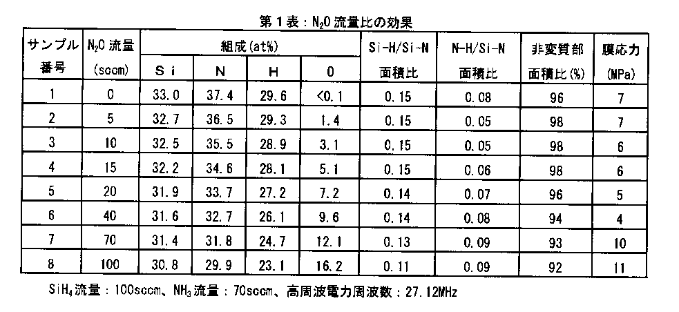
第1表から、SiH4に対するN2Oの流量比の低下に伴って、概してSi-H/Si-N面積比が減少する一方、N-H/Si-N面積比はN2O流量が5から20sccmの範囲で小さくなり、その後N2O流量を増やすと、N-H/Si-N面積比は大きくなることが分かる。
本製造例においては、アンモニアの流量を70sccm、亜酸化窒素流量を10sccmに固定し、および印加する高周波電力の周波数を40.68MHzまたは13.56MHz変更したことを除いて製造例1と同様の手順により、被成膜基板上にSiN:H膜を形成した。得られたSiN:H膜に関して、製造例1と同様の評価を行った。結果を第2表に示す。

第2表から、40.68MHzの高周波電力を用いた作製したサンプル11は、27.12MHzの高周波電力を用いた作製したサンプル7と同様に、優れた特性を示すことが明らかとなった。一方、13.56MHzの高周波電力を用いて作製したサンプル12においては、膜中の窒素および水素含有量が増大すると同時に、Si-H/Si-N面積比およびN-H/Si-N面積比がともに増大する現象が観察された。これは、反応室内でSiH4およびNH3、N2Oが十分に分解されないことに起因すると考えられる。この膜質の変化により、サンプル10の非変質部面積比が著しく低下した。すなわち、SiON:H膜の防湿性が著しく低下していることが分かった。
<実施例1>
本実施例においては、画素数2×2、画素幅0.3mm×0.3mmの赤色発光有機ELデバイスを作製する。
次に、下部電極を形成した基板を抵抗加熱蒸着装置内に設置した。マスクを使用した蒸着法によって、下部電極21の上に膜厚1.5nmのLiからなるバッファ層を形成した。引き続いて、蒸着法を用いて、電子輸送層/発光層/正孔輸送層/正孔注入層の4層からなる有機EL層を形成した。電子輸送層は膜厚20nmのAlq3であり、発光層は膜厚30nmのDPVBiであり、正孔輸送層は膜厚10nmのα-NPDであり、正孔注入層は膜厚100nmのCuPcであった。有機EL層の成膜の際には、装置の真空槽の内圧を1×10-4Paとし、0.1nm/sの成膜速度で各層を形成した。引き続いて、蒸着法を用いて、膜厚5nmのMgAg膜を形成して、ダメージ緩和層を形成した。
次に、上部電極を形成した積層体をプラズマCVD装置に移動させ、製造例1のサンプル3の条件を用いてSiON:H膜を堆積させ、保護層を形成した。すなわち、モノシラン、アンモニア、亜酸化窒素および窒素の混合ガスを原料として用い、周波数27.12MHzおよび電力密度0.5W/cm2の高周波電力を印加して、SiON:H膜を形成した。このとき、モノシラン、アンモニア、亜酸化窒素および窒素の流量は、それぞれ100sccm、80sccm、10sccm、2000sccmとした。また、成膜時の装置内圧力を100Paとし、被成膜基板を担持するステージの温度を50℃とした。以上の工程により、基板上に下部電極/有機EL層/上部電極/保護層からなる有機EL素子を形成した。得られた有機EL素子を、内部環境を酸素濃度5ppm以下および水分濃度5ppm以下に調整した貼り合わせ装置内に移動させた。
<比較例1>
保護層として用いるSiN:H膜の形成を、製造例1のサンプル1と同様に行ったことを除いて実施例1の手順を繰り返して、有機ELデバイスを形成した。すなわち、SiN:H膜形成時のアンモニアの流量を70sccmに変更して、有機ELデバイスの形成を行った。
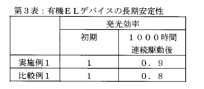
比較例1のデバイスは、実施例1と比較して1000時間連続駆動後の発光効率が低下することが分かる。比較例1のデバイスにおいては、保護層として用いたSiN:H膜を通した水分の侵入によって、発光効率の低下が進行したと考えられる。
Claims (6)
- 基板と、前記基板上に形成される有機EL素子とを含む有機ELデバイスであって、
前記有機EL素子は、下部電極、有機EL層、上部電極および保護層からなり、
前記保護層は、1つまたは複数の無機膜からなり、
前記1つまたは複数の無機膜の少なくとも1つは、水素を含む酸窒化ケイ素膜であり、
赤外吸収スペクトル測定によって求められるストレッチングモードのピーク面積比が、前記水素を含む酸窒化ケイ素膜中のSi-N結合に対するN-H結合の吸収面積比は0.05より大きく0.07以下であり、かつ、Si-N結合に対するSi-H結合の吸収面積比は0.15以下である
ことを特徴とする有機ELデバイス。 - 前記保護層は前記基板と前記下部電極との間に位置することを特徴とする請求項1に記載の有機ELデバイス。
- 前記保護層は前記上部電極の上面に位置することを特徴とする請求項1に記載の有機ELデバイス。
- 前記1つまたは複数の無機膜のそれぞれの応力は、20MPaより小さい絶対値を有することを特徴とする請求項1から3のいずれかに記載の有機ELデバイス。
- 前記N-H結合、Si-H結合、およびSi-N結合の吸収面積は、(a)波数を横軸とする酸窒化ケイ素膜の赤外吸収スペクトルを測定する工程、(b)得られた赤外吸収スペクトルからベースラインを減算する補正をする工程、(c)前記N-H結合、Si-H結合、およびSi-N結合の吸収をガウス関数を用いてピーク分離する工程、および(d)分離されたピークの面積を求める工程によって求められ、
前記N-H結合の吸収面積は、3250~3400cm-1に存在するピークから求められ、前記Si-H結合の吸収面積は、2100~2200cm-1に存在するピークから求められ、前記Si-N結合の吸収面積は、830~870cm-1に存在するピークから求められる
ことを特徴とする請求項1に記載の有機ELデバイス。 - (1) 基板を準備する工程と
(2) 下部電極、有機EL層、上部電極および保護層からなる有機EL素子を形成する工程であって、前記保護層は、水素を含む酸窒化ケイ素膜であり、赤外吸収スペクトル測定によって求められるストレッチングモードのピーク面積比が、前記水素を含む酸窒化ケイ素膜中のSi-N結合に対するN-H結合の吸収面積比は0.05より大きく0.07以下であり、かつ、Si-N結合に対するSi-H結合の吸収面積比は0.15以下である工程と
を含み、
工程(2)において、前記水素を含む酸窒化ケイ素膜は、モノシラン、アンモニアおよび窒素を含む混合ガスに対して25MHz以上60MHz以下の高周波電力を印加する化学的気相成長法によって形成され、ここで、モノシランに対するアンモニアの流量比は0.5以上1以下、モノシランに対するN2Oの流量比は、0よりも大きく、0.2よりも小さい
ことを特徴とする有機ELデバイスの製造方法。
Priority Applications (4)
| Application Number | Priority Date | Filing Date | Title |
|---|---|---|---|
| JP2010526587A JP5172961B2 (ja) | 2008-08-26 | 2009-04-06 | 有機elデバイスおよびその製造方法 |
| CN200980125797.5A CN102084716B (zh) | 2008-08-26 | 2009-04-06 | 有机el器件及其制造方法 |
| US13/003,674 US8492751B2 (en) | 2008-08-26 | 2009-04-06 | Organic EL device and process for manufacturing same |
| KR1020107028665A KR101246960B1 (ko) | 2008-08-26 | 2009-04-06 | 유기 el 디바이스 및 그 제조 방법 |
Applications Claiming Priority (4)
| Application Number | Priority Date | Filing Date | Title |
|---|---|---|---|
| JP2008216871 | 2008-08-26 | ||
| JP2008-216871 | 2008-08-26 | ||
| JP2008245914 | 2008-09-25 | ||
| JP2008-245914 | 2008-09-25 |
Publications (1)
| Publication Number | Publication Date |
|---|---|
| WO2010023987A1 true WO2010023987A1 (ja) | 2010-03-04 |
Family
ID=41721165
Family Applications (1)
| Application Number | Title | Priority Date | Filing Date |
|---|---|---|---|
| PCT/JP2009/057073 Ceased WO2010023987A1 (ja) | 2008-08-26 | 2009-04-06 | 有機elデバイスおよびその製造方法 |
Country Status (5)
| Country | Link |
|---|---|
| US (1) | US8492751B2 (ja) |
| JP (1) | JP5172961B2 (ja) |
| KR (1) | KR101246960B1 (ja) |
| CN (1) | CN102084716B (ja) |
| WO (1) | WO2010023987A1 (ja) |
Cited By (2)
| Publication number | Priority date | Publication date | Assignee | Title |
|---|---|---|---|---|
| EP2309022A1 (en) * | 2009-09-17 | 2011-04-13 | Fujifilm Corporation | Gas barrier coating and gas barrier film |
| JP2016522532A (ja) * | 2013-03-14 | 2016-07-28 | アプライド マテリアルズ インコーポレイテッドApplied Materials,Incorporated | 薄膜封入−oledに適用する薄型超高度バリア層 |
Families Citing this family (7)
| Publication number | Priority date | Publication date | Assignee | Title |
|---|---|---|---|---|
| WO2011013275A1 (ja) * | 2009-07-28 | 2011-02-03 | シャープ株式会社 | 有機素子及びそれを備えた有機デバイス |
| JP5659511B2 (ja) * | 2010-03-11 | 2015-01-28 | 住友化学株式会社 | 電気装置 |
| JP5369240B2 (ja) * | 2012-02-28 | 2013-12-18 | 日東電工株式会社 | 有機el素子の製造方法及び有機el素子 |
| CN106159669A (zh) * | 2016-08-23 | 2016-11-23 | 四川大学 | 基于氧化锌纳米棒的随机激光器及其激光增益介质制作方法 |
| US12255273B2 (en) * | 2019-02-15 | 2025-03-18 | Samsung Display Co., Ltd. | Display device and method for fabricating the same |
| CN110797255B (zh) * | 2019-10-14 | 2022-10-28 | 长江存储科技有限责任公司 | 薄膜堆叠结构、三维存储器及其制备方法 |
| CN111584744A (zh) * | 2020-05-13 | 2020-08-25 | 深圳市华星光电半导体显示技术有限公司 | 显示面板及其制备方法 |
Citations (6)
| Publication number | Priority date | Publication date | Assignee | Title |
|---|---|---|---|---|
| JPH06291114A (ja) * | 1993-03-31 | 1994-10-18 | Ricoh Co Ltd | 半導体装置 |
| JP2004335127A (ja) * | 2003-04-30 | 2004-11-25 | Shimadzu Corp | 有機el用保護膜の成膜装置、製造方法および有機el素子 |
| JP2005285659A (ja) * | 2004-03-30 | 2005-10-13 | Toyota Industries Corp | 有機el装置及びその製造方法 |
| JP2006261073A (ja) * | 2005-03-18 | 2006-09-28 | Seiko Epson Corp | 有機半導体装置の製造方法、有機半導体装置および電子機器 |
| JP2007123067A (ja) * | 2005-10-28 | 2007-05-17 | Seiko Epson Corp | 発光装置および電子機器 |
| JP2008214677A (ja) * | 2007-03-01 | 2008-09-18 | Toyota Central R&D Labs Inc | バリア膜及びバリア膜の製造方法 |
Family Cites Families (6)
| Publication number | Priority date | Publication date | Assignee | Title |
|---|---|---|---|---|
| JP2000012536A (ja) * | 1998-06-24 | 2000-01-14 | Tokyo Ohka Kogyo Co Ltd | シリカ被膜形成方法 |
| KR100499171B1 (ko) * | 2003-07-21 | 2005-07-01 | 삼성전자주식회사 | 스핀온글래스에 의한 산화실리콘막의 형성방법 |
| CN100466328C (zh) | 2003-10-29 | 2009-03-04 | 铼宝科技股份有限公司 | 有机发光显示面板 |
| JP4479249B2 (ja) * | 2004-01-20 | 2010-06-09 | 凸版印刷株式会社 | 有機el素子の製造方法 |
| JP2007213914A (ja) * | 2006-02-08 | 2007-08-23 | Canon Inc | 有機el素子アレイ |
| KR20110040616A (ko) * | 2008-07-24 | 2011-04-20 | 후지 덴키 홀딩스 가부시키가이샤 | 유기 el 디바이스 및 그 제조 방법 |
-
2009
- 2009-04-06 CN CN200980125797.5A patent/CN102084716B/zh not_active Expired - Fee Related
- 2009-04-06 US US13/003,674 patent/US8492751B2/en not_active Expired - Fee Related
- 2009-04-06 WO PCT/JP2009/057073 patent/WO2010023987A1/ja not_active Ceased
- 2009-04-06 KR KR1020107028665A patent/KR101246960B1/ko not_active Expired - Fee Related
- 2009-04-06 JP JP2010526587A patent/JP5172961B2/ja not_active Expired - Fee Related
Patent Citations (6)
| Publication number | Priority date | Publication date | Assignee | Title |
|---|---|---|---|---|
| JPH06291114A (ja) * | 1993-03-31 | 1994-10-18 | Ricoh Co Ltd | 半導体装置 |
| JP2004335127A (ja) * | 2003-04-30 | 2004-11-25 | Shimadzu Corp | 有機el用保護膜の成膜装置、製造方法および有機el素子 |
| JP2005285659A (ja) * | 2004-03-30 | 2005-10-13 | Toyota Industries Corp | 有機el装置及びその製造方法 |
| JP2006261073A (ja) * | 2005-03-18 | 2006-09-28 | Seiko Epson Corp | 有機半導体装置の製造方法、有機半導体装置および電子機器 |
| JP2007123067A (ja) * | 2005-10-28 | 2007-05-17 | Seiko Epson Corp | 発光装置および電子機器 |
| JP2008214677A (ja) * | 2007-03-01 | 2008-09-18 | Toyota Central R&D Labs Inc | バリア膜及びバリア膜の製造方法 |
Cited By (2)
| Publication number | Priority date | Publication date | Assignee | Title |
|---|---|---|---|---|
| EP2309022A1 (en) * | 2009-09-17 | 2011-04-13 | Fujifilm Corporation | Gas barrier coating and gas barrier film |
| JP2016522532A (ja) * | 2013-03-14 | 2016-07-28 | アプライド マテリアルズ インコーポレイテッドApplied Materials,Incorporated | 薄膜封入−oledに適用する薄型超高度バリア層 |
Also Published As
| Publication number | Publication date |
|---|---|
| JPWO2010023987A1 (ja) | 2012-01-26 |
| US20110186822A1 (en) | 2011-08-04 |
| CN102084716B (zh) | 2014-05-14 |
| KR20110020271A (ko) | 2011-03-02 |
| JP5172961B2 (ja) | 2013-03-27 |
| KR101246960B1 (ko) | 2013-03-25 |
| US8492751B2 (en) | 2013-07-23 |
| CN102084716A (zh) | 2011-06-01 |
Similar Documents
| Publication | Publication Date | Title |
|---|---|---|
| JP5378354B2 (ja) | 有機elデバイスおよびその製造方法 | |
| JP5172961B2 (ja) | 有機elデバイスおよびその製造方法 | |
| JP4493216B2 (ja) | 有機エレクトロルミネッセンス素子およびその製造方法 | |
| US8847219B2 (en) | Color conversion film and multicolor-emitting, organic electroluminescent device comprising the color conversion film | |
| JPWO2000060905A1 (ja) | 有機エレクトロルミネッセンス素子およびその製造方法 | |
| TW200428901A (en) | Organic light-emitting display | |
| WO2010010622A1 (ja) | 有機elデバイスおよびその製造方法 | |
| TWI538552B (zh) | 有機el裝置 | |
| JP2004039468A (ja) | 有機elカラーディスプレイ | |
| WO2000072637A1 (en) | Organic el color display | |
| WO2009099009A1 (ja) | 有機elディスプレイおよびその製造方法 | |
| JP2008140621A (ja) | 有機elディスプレイおよびその製造方法 | |
| JP2010244860A (ja) | 有機el素子およびその製造方法 |
Legal Events
| Date | Code | Title | Description |
|---|---|---|---|
| WWE | Wipo information: entry into national phase |
Ref document number: 200980125797.5 Country of ref document: CN |
|
| 121 | Ep: the epo has been informed by wipo that ep was designated in this application |
Ref document number: 09809642 Country of ref document: EP Kind code of ref document: A1 |
|
| WWE | Wipo information: entry into national phase |
Ref document number: 2010526587 Country of ref document: JP |
|
| ENP | Entry into the national phase |
Ref document number: 20107028665 Country of ref document: KR Kind code of ref document: A |
|
| NENP | Non-entry into the national phase |
Ref country code: DE |
|
| WWE | Wipo information: entry into national phase |
Ref document number: 13003674 Country of ref document: US |
|
| 122 | Ep: pct application non-entry in european phase |
Ref document number: 09809642 Country of ref document: EP Kind code of ref document: A1 |