WO2010016178A1 - 表示装置及びその製造方法 - Google Patents
表示装置及びその製造方法 Download PDFInfo
- Publication number
- WO2010016178A1 WO2010016178A1 PCT/JP2009/002577 JP2009002577W WO2010016178A1 WO 2010016178 A1 WO2010016178 A1 WO 2010016178A1 JP 2009002577 W JP2009002577 W JP 2009002577W WO 2010016178 A1 WO2010016178 A1 WO 2010016178A1
- Authority
- WO
- WIPO (PCT)
- Prior art keywords
- insulating film
- display device
- interlayer insulating
- connection terminals
- substrate
- Prior art date
Links
Images


Classifications
-
- G—PHYSICS
- G02—OPTICS
- G02F—OPTICAL DEVICES OR ARRANGEMENTS FOR THE CONTROL OF LIGHT BY MODIFICATION OF THE OPTICAL PROPERTIES OF THE MEDIA OF THE ELEMENTS INVOLVED THEREIN; NON-LINEAR OPTICS; FREQUENCY-CHANGING OF LIGHT; OPTICAL LOGIC ELEMENTS; OPTICAL ANALOGUE/DIGITAL CONVERTERS
- G02F1/00—Devices or arrangements for the control of the intensity, colour, phase, polarisation or direction of light arriving from an independent light source, e.g. switching, gating or modulating; Non-linear optics
- G02F1/01—Devices or arrangements for the control of the intensity, colour, phase, polarisation or direction of light arriving from an independent light source, e.g. switching, gating or modulating; Non-linear optics for the control of the intensity, phase, polarisation or colour
- G02F1/13—Devices or arrangements for the control of the intensity, colour, phase, polarisation or direction of light arriving from an independent light source, e.g. switching, gating or modulating; Non-linear optics for the control of the intensity, phase, polarisation or colour based on liquid crystals, e.g. single liquid crystal display cells
- G02F1/133—Constructional arrangements; Operation of liquid crystal cells; Circuit arrangements
- G02F1/136—Liquid crystal cells structurally associated with a semi-conducting layer or substrate, e.g. cells forming part of an integrated circuit
- G02F1/1362—Active matrix addressed cells
-
- G—PHYSICS
- G02—OPTICS
- G02F—OPTICAL DEVICES OR ARRANGEMENTS FOR THE CONTROL OF LIGHT BY MODIFICATION OF THE OPTICAL PROPERTIES OF THE MEDIA OF THE ELEMENTS INVOLVED THEREIN; NON-LINEAR OPTICS; FREQUENCY-CHANGING OF LIGHT; OPTICAL LOGIC ELEMENTS; OPTICAL ANALOGUE/DIGITAL CONVERTERS
- G02F1/00—Devices or arrangements for the control of the intensity, colour, phase, polarisation or direction of light arriving from an independent light source, e.g. switching, gating or modulating; Non-linear optics
- G02F1/01—Devices or arrangements for the control of the intensity, colour, phase, polarisation or direction of light arriving from an independent light source, e.g. switching, gating or modulating; Non-linear optics for the control of the intensity, phase, polarisation or colour
- G02F1/13—Devices or arrangements for the control of the intensity, colour, phase, polarisation or direction of light arriving from an independent light source, e.g. switching, gating or modulating; Non-linear optics for the control of the intensity, phase, polarisation or colour based on liquid crystals, e.g. single liquid crystal display cells
- G02F1/133—Constructional arrangements; Operation of liquid crystal cells; Circuit arrangements
- G02F1/1333—Constructional arrangements; Manufacturing methods
- G02F1/1345—Conductors connecting electrodes to cell terminals
- G02F1/13458—Terminal pads
Definitions
- the present invention relates to a display device and a manufacturing method thereof.
- a display device generally has a display panel in which a switching element substrate and a counter substrate are bonded to each other and a display medium layer is sandwiched between the substrates. With such a configuration, the amount of transmitted light is controlled according to the potential difference applied between the pixel electrode formed on the switching element substrate and the common electrode formed on the counter substrate, and the display screen has a predetermined gradation. An image can be displayed.
- an active matrix substrate configured by arranging switching elements in a matrix for each pixel is widely used as a switching element substrate.
- such an active matrix substrate is formed with a plurality of connection terminals that are electrically connected to the switching elements and pulled out in order to send driving signals to the respective switching elements.
- Patent Documents 1 and 2 disclose a configuration near the connection terminal of such an active matrix substrate, a manufacturing method, and the like.
- FIG. 19 is a plan view of the connection terminal region of the active matrix substrate.
- 20A to 20C are cross-sectional views of the connection terminal region in each manufacturing process of the active matrix substrate.
- FIG. 20C corresponds to a cross section taken along line I-I ′ of FIG.
- a plurality of switching elements are arranged in a matrix on an insulating substrate 100. Further, in order to send a driving signal to the switching element, a plurality of connection terminals 101 are formed which are electrically connected to the switching element and drawn out, and arranged in parallel to each other.
- an interlayer insulating film 102 is formed on the insulating substrate 100 on which the switching elements and connection terminals 101 are formed. At this time, a contact hole that leads to the switching element is formed in the interlayer insulating film 102, and further, the tips of the plurality of connection terminals 101 are exposed.
- a pixel electrode material 103 made of, for example, ITO (indium tin oxide) is formed on the entire surface of the insulating substrate 100 on which the interlayer insulating film 102 is formed.
- a photosensitive resist 104 is provided on the pixel electrode material 103, exposed and developed.
- the end portion of the interlayer insulating film 102 has a steep inclination angle of about 70 °. Therefore, the thickness (R 1) of the photosensitive resist 104 provided above the interlayer insulating film 102 and the end of the insulating substrate 100.
- the thickness (R2) of the photosensitive resist 104 provided above the vicinity of the end portion of the interlayer insulating film 102 is larger than the thickness (R3) of the photosensitive resist 104 provided above the connection terminal 101 extending in the area. Yes.
- the photosensitive resist 104 is exposed and developed.
- the photosensitive resist 104 provided above the vicinity of the end portion of the interlayer insulating film 102 has a large thickness (R2) as described above, and thus is not completely removed, as shown in FIG. Residue 104 'is produced.
- a pixel electrode having a predetermined pattern is formed by etching using the photosensitive resist 104 as a mask. At this time, since the residue 104 ′ of the photosensitive resist 104 is generated at the end portion of the interlayer insulating film 102, as shown in FIG. 105 is generated.
- the pixel electrode residue 105 When the pixel electrode residue 105 is generated at the end of the interlayer insulating film 102 as described above, the pixel electrode residue 105 electrically connects the adjacent connection terminals 101 as shown in FIG. There is a problem in that a leakage current is generated between both terminals, causing a display defect.
- the present invention has been made in view of such a problem, and an object of the present invention is to provide a display device having a good display quality and manufacturing efficiency and a manufacturing method thereof.
- a display device is a display device comprising: an active matrix substrate in which a plurality of switching elements are arranged in a matrix; and a counter substrate arranged to face the active matrix substrate via a display medium layer.
- the active matrix substrate is pulled out by being electrically connected to each switching element and sending a driving signal to the switching element, and a plurality of connection terminals arranged in parallel to each other, a plurality of switching elements and a plurality of connections
- the interlayer insulating film is provided on the terminal, and is provided on the exposed region of the interlayer insulating film and the plurality of connection terminals, so that the ends of the plurality of connection terminals are exposed at the ends.
- the opening may be formed in a rectangular shape.
- the length from the tip of the opening to the tip of the interlayer insulating film may be 10 ⁇ m or less.
- the length of the opening in the direction perpendicular to the direction in which the plurality of connection terminals extend may be 9.5 to 13.5 ⁇ m or more.
- the opening may be formed to extend onto any one of the adjacent connection terminals.
- a plurality of openings may be formed in parallel in a direction from one adjacent connection terminal to the other connection terminal.
- At least one of the plurality of openings may be formed to extend onto the adjacent connection terminal.
- the display medium may be made of a liquid crystal material.
- the pixel electrode may be made of indium tin oxide or indium zinc oxide.
- the switching element may be a thin film transistor.
- a display device manufacturing method includes: an active matrix substrate in which a plurality of switching elements are arranged in a matrix; and a counter substrate arranged to face the active matrix substrate via a display medium layer.
- the contact holes are provided on the plurality of switching elements and the plurality of connection terminals and communicate with the switching elements, and the ends of the plurality of connection terminals are exposed at the ends, and the interlayer insulation is provided.
- FIG. 1 is a cross-sectional view of a liquid crystal display device according to an embodiment of the present invention. It is sectional drawing of the thin-film transistor substrate which concerns on embodiment of this invention. It is a top view of a thin-film transistor substrate provided with a rectangular opening. It is sectional drawing in each manufacturing process of the connection terminal area
- FIG. 1 It is a top view of a thin-film transistor substrate provided with the opening part in which the some corner
- FIG. 6 is a plan view of a photomask and a thin film transistor substrate in which a plurality of rectangular openings are arranged in parallel at equal intervals at the end. It is a top view of a photomask and a thin film transistor substrate provided with a plurality of substantially rectangular openings arranged in parallel two by two. It is a top view of the thin film transistor substrate in which a plurality of openings are formed toward the inner side of the interlayer insulating film. It is a top view of the thin-film transistor substrate in which the opening part provided in parallel was formed in multiple numbers toward the inner side of the interlayer insulation film.
- region in each manufacturing process of the conventional active matrix substrate is sectional drawing of the connection terminal area
- a configuration of a display device according to an embodiment of the present invention and a manufacturing method thereof will be described in detail based on the drawings.
- a liquid crystal display device will be described as an example of the display device.
- the present invention is not limited to the following embodiment.
- FIG. 1 shows a cross-sectional view of a liquid crystal display device 10 according to an embodiment of the present invention.
- the liquid crystal display device 10 includes a liquid crystal display panel 11 and a backlight 12.
- the liquid crystal display panel 11 includes a thin film transistor substrate 13 (active matrix substrate) having a polarizing plate 18 disposed on the outer surface, a color filter substrate 14 (counter substrate) having a polarizing plate 28 disposed on the outer surface, a thin film transistor substrate 13, And a liquid crystal layer 15 (display medium layer) sandwiched between the color filter substrates 14.
- the liquid crystal layer 15 is surrounded by a sealing material 29 that bonds the thin film transistor substrate 13 and the color filter substrate 14 together.
- a black matrix (light-shielding film), a color filter, a counter electrode (not shown), and an alignment film 27 are formed on the surface of the glass substrate serving as the base of the color filter substrate 14 on the liquid crystal layer 15 side.
- a plurality of gate lines extending in the X-axis direction and a plurality of source lines (not shown) extending in the Y-axis direction are formed on the thin film transistor substrate 13.
- Each rectangular area defined by these gate lines and source lines is a pixel area.
- Thin film transistors (switching elements) 40 are respectively formed at portions where a plurality of gate lines and source lines intersect.
- FIG. 2 is a cross-sectional view of the thin film transistor 40 portion of the thin film transistor substrate 13.
- the thin film transistor substrate 13 includes a glass substrate 30 (insulating substrate) serving as a base. In addition to the glass substrate 30, a resin substrate or the like may be used as an insulating substrate.
- a gate electrode 31 is formed on the glass substrate 30.
- a gate insulating film 32 made of, for example, SiO 2 or SiN is formed on the gate electrode 31.
- a semiconductor film 33 (operating semiconductor film) that becomes an active layer of the thin film transistor 40 is formed.
- the semiconductor film 33 includes a channel region, and a channel protective film 34 made of an insulating material such as SiO 2 or SiN is formed on the channel region of the semiconductor film 33.
- n + semiconductor film 35 is formed on the semiconductor film 33 and the channel protective film 34, and is formed of Al, Ta, MoW alloy, Cr, or the like across the channel protective film 34 via the n + semiconductor film 35.
- a source electrode 36 and a drain electrode 37 are formed apart from each other.
- a pixel electrode 39 provided in the pixel region is electrically connected to the drain electrode 37 via an interlayer insulating film 38 made of an insulating material such as SiO 2 or SiN.
- the pixel electrode 39 is formed of a transparent conductor such as ITO (indium tin oxide) or IZO (indium zinc oxide).
- An alignment film 17 made of polyimide or the like is formed on the pixel electrode 39.
- a connection terminal 41 for receiving an external signal is formed at the end of the thin film transistor substrate 13 and is drawn from the source line.
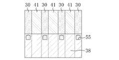
- FIG. 3A is a plan view of the connection terminal 41 region of the thin film transistor substrate 13.
- FIG. 4D is a cross-sectional view taken along line I-I ′ in FIG.
- the thin film transistor substrate 13 is formed on the glass substrate 30 and the glass substrate 30 in a region where the connection terminal 41 of the thin film transistor substrate 13 is provided, and is equidistant from each other.
- the connection terminal 41 is provided on the glass substrate 30 and the glass substrate 30 in a region where the connection terminal 41 of the thin film transistor substrate 13 is provided, and is equidistant from each other.
- an interlayer insulating film 38 provided also on the thin film transistor 40 is formed. The end portions of the interlayer insulating film 38 are formed so that the tips of the plurality of connection terminals 41 are exposed.
- connection terminal 41 is configured to be drawn from the source line to the end of the thin film transistor substrate 13.
- connection terminal 41 is not necessarily a terminal related to the wiring drawn from the source line, and is drawn from the gate line. It may be a terminal related to wiring.
- Openings 50 reaching the glass substrate 30 are formed in regions corresponding to the portions between the plurality of connection terminals 41 at the end of the interlayer insulating film 38.
- the opening 50 is formed in a rectangular shape. As shown in FIG. 3A, the opening 50 has a short length from the tip of the opening 50 to the tip of the interlayer insulating film 38 (that is, from the tip of the opening 50 to the tip of the interlayer insulating film 38). And the length from the tip of the opening 50 to the tip of the interlayer insulating film 38 is longer (that is, the opening is as shown in FIGS. 3B and 3C). The length from the tip of the portion 50 to the tip of the interlayer insulating film 38 is L2 or L3 which is longer than L1).
- the length from the tip of the opening 50 to the tip of the interlayer insulating film 38 can be selected as appropriate from among these, and the opening 50 has the film thicknesses of a plurality of films constituting the thin film transistor substrate 13 and the like. Therefore, it can be formed at an optimal position where the effects of the present invention are exhibited.
- the lengths L1 to L3 from the tip of the opening 50 to the tip of the interlayer insulating film 38 are set to 10 ⁇ m or less, preferably 3 to 7.2 ⁇ m, more preferably 3 to 6 ⁇ m. ing.
- the opening 50 has a predetermined length (L4) determined in the longitudinal direction parallel to the direction in which the plurality of connection terminals 41 extend, and the plurality of connection terminals.
- the lateral length perpendicular to the direction in which 41 extends is long (that is, the lateral length shown in FIG. 5 (a) is W1) and even shorter (that is, FIG. 5 (b)).
- the length in the lateral direction is appropriately selected from these, and can be formed into an optimum shape that exhibits the effects of the present invention in relation to the film thicknesses of a plurality of films constituting the thin film transistor substrate 13. .
- the longitudinal length L4 parallel to the direction in which the plurality of connection terminals 41 extends is 20 ⁇ m
- the lateral lengths W1 to W3 perpendicular to the direction in which the plurality of connection terminals 41 extend are 9.5. It is formed to ⁇ 13.5 ⁇ m.
- the opening 50 may not be formed in a rectangular shape, and may be formed, for example, in the shape shown in FIGS.
- FIG. 6 shows a thin film transistor substrate provided with an opening 51 formed in an elliptical shape.
- FIG. 7 shows a thin film transistor substrate provided with a circular opening 52.
- FIG. 8 shows a thin film transistor substrate provided with an opening 53 formed in a pentagonal shape so that the cusp is directed toward the tip.
- the opening part 50 may be formed in polygonal shapes other than rectangular shape or pentagon shape.
- FIG. 9 shows a thin film transistor substrate provided with an opening 54 in which a plurality of corners are formed in the distal direction.
- FIG. 10 shows a thin film transistor substrate provided with an opening 55 whose tip direction is formed in a wave shape.
- FIG. 11 shows a thin film transistor substrate provided with an opening 56 formed in a trapezoidal shape having a hypotenuse in the distal direction.
- the openings 54 and 55 shown in FIGS. 9 to 10 may be formed upside down in FIGS. 9 to 10, that is, so that the protruding structure is directed toward the rear end of the interlayer insulating film 38. . According to such a structure, even if the openings 54 and 55 are formed so as to straddle the adjacent connection terminals 41, the effects of the present invention can be obtained in the same manner, so that the degree of freedom in design is good. .
- the opening 50 may be formed to extend onto the adjacent connection terminal 41.
- FIG. 12 shows an opening 57 formed so as to extend onto one adjacent connection terminal 41.
- FIG. 13 shows two openings 58 formed in parallel in the direction from one adjacent connection terminal 41 to the other connection terminal 41, each extending to the connection terminal 41.
- the shape of the opening 50 may be other, but the adjacent connection terminals 41 should not be connected by the opening 50, and a wall of the interlayer insulating film 38 is always formed between the connection terminals 41. It must be. This is because if the connection portions 41 adjacent to each other are connected by the opening 50, there is a region in which both terminals are not insulated and conductive.
- connection terminal 41 region has a structure as shown in FIG. 4D shows a cross section of the interlayer insulating film 38 having the opening 50 on the front side, and shows a connection terminal 41 adjacent to the back side and a pixel electrode 39 patterned on the connection terminal 41.
- the end portion of the interlayer insulating film 38 adjacent to the connection terminal 41 has a small raised portion 60 from the tip of the opening 50 to the tip of the interlayer insulating film 38 and a portion 61 that rises from the rear end of the opening 50 toward the pixel region. And is composed of.
- the thickness T1 of the small raised portion 60 from the tip of the opening 50 to the tip of the interlayer insulating film 38 is smaller than the thickness T2 of the portion 61 that rises from the rear end of the opening 50 toward the pixel region. It is formed in about half. More specifically, the thickness T1 of the small raised portion 60 from the tip of the opening 50 to the tip of the interlayer insulating film 38 is, for example, about 1.5 ⁇ m. A thickness T2 of the portion 61 that rises toward the region is, for example, about 2.5 to 3.0 ⁇ m.
- a glass substrate 30 serving as a base of the thin film transistor substrate 13 is prepared. Then, a metal film having a thickness of about 0.5 ⁇ m is formed on the glass substrate 30 by sputtering using, for example, an Al alloy.
- a resist mask is formed by exposing and developing on the metal film using a photomask, and then gate lines, gate electrodes 31 and the like are formed by dry etching.
- SiN is formed on the entire surface of the substrate with a thickness of about 0.6 ⁇ m by the plasma CVD method to form the gate insulating film 32.
- a Si layer for forming the semiconductor film 33 is formed on the entire surface of the substrate with a thickness of about 30 nm by a high-density plasma CVD method.
- a protective film material layer (for example, SiN) for forming the channel protective film 34 is formed on the entire surface of the substrate with a film thickness of about 150 nm by plasma CVD.
- a resist for leaving the protective film material layer in a region corresponding to the channel region of the semiconductor film 33 is formed by patterning.
- the protective film material layer is patterned by an etching and resist peeling process to form a channel protective film 34.
- n + semiconductor film 35 for example, n + amorphous Si
- a metal film such as Ti are sequentially formed.
- a photoresist is formed on the entire surface of the substrate, exposed using a mask, and developed to pattern the resist.
- plasma dry etching is performed to connect the source line, the connection terminal 41 drawn from the source line to the edge of the substrate, the source electrode 36, the drain electrode 37, the n + semiconductor film 35, and the semiconductor film 33 is formed.
- an interlayer insulating film material for example, SiN is formed on the entire surface of the substrate with a thickness of about 3.0 ⁇ m by plasma CVD.
- FIG. 14 the interlayer insulating film material is exposed and developed using a photomask 63 in which a plurality of rectangular openings 62 are arranged in parallel at the ends at the end, thereby developing the thin film transistor 40.
- An interlayer insulating film 38 is formed, which has contact holes that lead to the ends of the plurality of connection terminals 41 at the ends.
- the rectangular opening 50 described above is formed in the interlayer insulating film 38 in a region corresponding to the portion between the plurality of connection terminals 41 at the end so as to correspond to the opening 62 of the photomask 63.
- FIG. 4A shows a cross-sectional view of the interlayer insulating film 38 in the connection terminal 41 region at this time. As shown in FIG.
- the interlayer insulating film 38 has a small width L1 from the tip of the opening 50 to the tip of the interlayer insulating film 38. Therefore, a small rising portion is generated due to the intensity distribution of incident light during exposure.
- 60 thickness T1 is about 1.5 ⁇ m, for example
- a portion 61 is formed from the rear end of the opening 50 toward the pixel region.
- ITO 39 ' is formed as a pixel electrode material on the entire surface of the substrate to a film thickness of about 0.1 ⁇ m by sputtering.
- a photosensitive resist 64 is provided on the entire surface of the substrate.
- the end portion of the interlayer insulating film 38 includes a small raised portion 60 from the tip of the opening 50 to the tip of the interlayer insulating film 38 and a portion 61 that rises from the rear end of the opening 50 toward the pixel region. Since it is comprised, the photosensitive resist 64 is gently formed along those parts. Therefore, the difference in film thickness of the photosensitive resist 64 on the end region of the interlayer insulating film 38 is small.
- the photosensitive resist 64 is exposed and developed to form a pattern of the photosensitive resist 64 in the region where the ITO 39 'is left as shown in FIG. 4C.
- the difference in film thickness of the photosensitive resist 64 provided on the end region of the interlayer insulating film 38 is reduced, in FIG.
- the residue of the photosensitive resist 64 does not occur at the tip S1 of the small raised portion 60 up to the tip of the film 38.
- the pixel electrode 39 is formed by etching the ITO 39 'using the patterned photosensitive resist 64 as a mask. At this time, as described above, since the residue of the photosensitive resist 64 does not occur on the ITO 39 ′ that is the pixel electrode material, the pixel electrode 39 is accurately patterned on each connection terminal 41, and between the adjacent connection terminals 41. Thus, no residue of the pixel electrode 39 is generated.
- the photosensitive resist 64 is removed, and polyimide is applied to the entire surface of the substrate to form the alignment film 17. In this way, the thin film transistor substrate 13 is completed.
- a glass substrate serving as a base of the color filter substrate 14 is prepared. Then, a black matrix is formed from a metal such as Cr or a black resin on a predetermined region of the glass substrate. Next, red, green and blue color filters are formed on the glass substrate using a red photosensitive resin, a green photosensitive resin and a blue photosensitive resin. Next, after forming a counter electrode by sputtering a transparent conductive film such as ITO on the entire upper surface of the glass substrate, polyimide is applied on the counter electrode to form an alignment film 27. In this way, the color filter substrate 14 is completed.
- the thin film transistor substrate 13 and the color filter substrate 14 manufactured in this way are opposed to each other with a spacer (not shown) interposed therebetween, and are bonded together with a sealing material 29, and a liquid crystal material is sealed between the substrates, thereby a liquid crystal display panel. 11 is assumed.
- polarizing plates 18 and 28 are disposed on both sides of the liquid crystal display panel 11 in the thickness direction, and a drive circuit and a backlight 12 are attached. Thereby, the liquid crystal display device 10 is completed.
- the opening portion of the interlayer insulating film 38 has been described by taking the example of FIG. 3A as an example.
- the interlayer insulating film 38 material was exposed and developed using the photomask 63 in which the rectangular openings 62 are arranged in parallel at equal intervals.
- the photomask is appropriately selected depending on the type of the openings.
- the shape of the opening of the photomask is substantially the same as the shape of the opening formed in the interlayer insulating film 38.
- two interlayer insulating films are formed in parallel in the direction from one adjacent connection terminal 41 to the other connection terminal 41, and each extends over the connection terminal 41.
- a photomask 69 including the openings 68 having the shape shown in FIG. 15 may be used.
- the photomask 69 shown in FIG. 15 is provided with a plurality of substantially rectangular openings 68 arranged in parallel two by two so as to correspond to the openings 58 of the interlayer insulating film 38 of FIG.
- the two openings 68 arranged in parallel are formed with convex portions 70 at corners facing each other in the mask edge direction.
- the two openings 68 arranged in parallel are formed with a missing portion 71 in which corners facing each other in the direction opposite to the convex portion 70 are cut, and the interval between the two openings 68 is partially set. It is getting bigger. As described above, if the gap between the two openings 68 is partially increased, it is possible to satisfactorily suppress the connection between the two openings 68 of the interlayer insulating film 38 due to exposure and development.
- a plurality of openings 50 to 58 of the interlayer insulating film 38 may be arranged along the direction in which the connection terminal 41 extends. Specifically, as shown in FIG. 16, openings 50 ′′ and 50 ′ are formed in the inner direction of the interlayer insulating film 38 following the opening 50 ′ disposed at the tip of the interlayer insulating film 38. '',... May be arranged. Further, as shown in FIG. 17, at the tip of the interlayer insulating film 38, two are formed in parallel in a direction from one adjacent connection terminal 41 to the other connection terminal 41, and each extends to the connection terminal 41. The openings 58 ′′, 58 ′ ′′,...
- the shape of the opening is not limited to a rectangular shape, and may be any shape.
- the number of openings arranged one after the other from the front end of the interlayer insulating film 38 is not limited, but the opening arranged on the innermost side is one of the adjacent connection terminals 41.
- One opening should not be formed from one to the other. This is because there is a possibility that the adjacent connection terminal 41 may become conductive due to the ITO residue accumulated in the opening.
- the opening 58 of the interlayer insulating film 38 is not limited to two openings formed in parallel in the direction from one adjacent connection terminal 41 to the other connection terminal 41 at the tip of the interlayer insulating film 38, As shown in FIG. 18, a plurality of openings 58 ′, 58 ′′, 58 ′ ′′,... May be formed in parallel. Further, the number and shape of the openings arranged in parallel are not limited.
- an LCD liquid crystal display
- the display device is not limited to this.
- an organic EL organic electroluminescence
- an inorganic EL inorganic electroluminescence
- Electrophoretic PD (plasma display)
- PALC plasma addressed liquid crystal display
- FED field emission display
- SED surface-conduction electron-
- It may be a display device such as emitter display (surface electric field display).
- the liquid crystal display device 10 of the present invention is arranged in parallel in a direction from one adjacent connection terminal 41 to the other connection terminal 41 in a region corresponding to a portion between the plurality of connection terminals 41 at the end of the interlayer insulating film 38.
- An opening 57 is formed.
- the end portion of the interlayer insulating film 38 has a small raised portion 60 from the tip of the opening 57 to the tip of the interlayer insulating film 38 and a portion 61 that rises from the rear end of the opening 57 toward the pixel region. Composed.
- a photosensitive resist 64 for patterning the pixel electrode 39 is provided on the entire surface of the substrate, a small raised portion 60 from the front end of the opening 57 to the front end of the interlayer insulating film 38 and the rear end of the opening 57 to the pixel region.
- a photosensitive resist 64 is gently formed along the portion 61 that rises toward the top. Accordingly, the difference in film thickness of the photosensitive resist 64 on the end region of the interlayer insulating film 38 is reduced, and a residue of the photosensitive resist 64 is generated at the end of the interlayer insulating film 38 when the photosensitive resist 64 is removed. Can be satisfactorily suppressed. For this reason, the residue of the pixel electrode 39 formed corresponding to the residue of the photosensitive resist 64 is not generated, and it is possible to satisfactorily suppress the occurrence of a leak current between the adjacent connection terminals 41.
- the shape of the opening formed in the interlayer insulating film 38 is shown in FIGS. 3 and 5 to 13. However, any of these can provide at least the above-described effects.
- the thin film transistor substrate having the above-described configuration was subjected to an evaluation test for examining the relationship between the position / size of the opening of the interlayer insulating film and the occurrence state of the photosensitive resist residue.
- Example 1 As Example 1, as shown in FIGS. 3 and 5 in this embodiment, the opening has a rectangular shape, and the length (L4) in the vertical direction parallel to the direction in which the plurality of connection terminals extend is 19.5 ⁇ m.
- L4 and W1 have the same value, and an interlayer insulating film having L1 of 3.5 ⁇ m, 6.0 ⁇ m, and 7.2 ⁇ m, respectively, is formed. did.
- Example 1 L1 and L4 had the same value, and an interlayer insulating film having W1 of 9.5 ⁇ m was formed.
- Example 5 L4 and W1 have the same value, and an interlayer insulating film having L1 of 3.5 ⁇ m, 6.0 ⁇ m, and 7.2 ⁇ m, respectively, is formed, and Examples 6, 7, and 8, respectively. did.
- Example 9 With respect to Example 1, L1 and L4 had the same value, and an interlayer insulating film with W1 of 6.5 ⁇ m was formed, and Example 9 was obtained. In contrast to Example 9, L4 and W1 have the same value, and an interlayer insulating film having L1 of 3.5 ⁇ m, 6.0 ⁇ m, and 7.2 ⁇ m, respectively, is formed. did.
- Example 13 two are formed in parallel in the direction from one adjacent connection terminal to the other connection terminal as shown in FIG. 13 in this embodiment, and each extends to the connection terminal.
- An interlayer insulating film having a rectangular opening formed in this manner was formed.
- the interlayer insulating film of Example 13 has a vertical length (L4) of 19.5 ⁇ m and a horizontal length (W1) of 10.5 ⁇ m parallel to the direction in which the plurality of connection terminals extend in each opening. Further, the length (L1) from the tip to the tip of the interlayer insulating film was formed to 3.0 ⁇ m. The interval between adjacent openings was 5.5 ⁇ m.
- L4 and W1 have the same value, and an interlayer insulating film having L1 of 3.5 ⁇ m, 6.0 ⁇ m, and 7.2 ⁇ m, respectively, is formed. did.
- ITO as a pixel electrode material was formed to a thickness of 0.1 ⁇ m by sputtering on the entire surface of the substrate, and then a photosensitive resist was provided on the entire surface of the substrate.
- the photosensitive resist was exposed and developed to form a photosensitive resist pattern in the region where the ITO was to remain.
- the exposure amount was divided into three types (45, 50, 60 mJ / cm 2 ) and tested.
- connection terminals are formed by laminating a Ti film (350 mm), an Al film (3600 mm) and a Ti film (1000 mm), the width of each connection terminal is 50 ⁇ m, and the distance between them is 22 ⁇ m. .
- the film thickness of the interlayer insulating film provided on the entire surface of the substrate was 3.3 ⁇ m.
- Comparative example As a comparative example, a substrate having the same configuration as that of the example except that no opening was formed in the interlayer insulating film was prepared, and the state of the residue of the photosensitive resist was similarly confirmed.
- Table 1 shows the test results of the above-described Examples and Comparative Examples.
- the present invention is useful for a display device and a manufacturing method thereof.
Abstract
表示装置のアクティブマトリクス基板は、ガラス基板(30)と、当該ガラス基板の表面に形成され、互いに等間隔に並列配置された複数の接続端子(41)と、当該複数の接続端子を覆う層間絶縁膜(38)とを備える。当該層間絶縁膜の端部は、前記複数の接続端子の先端がそれぞれ剥き出しになるように形成される。前記層間絶縁膜の端部には、複数の開口部(58)が形成される。各開口部は、隣り合う2つの接続端子の間の領域から、前記2つの接続端子の一方の上まで延長される。 層間絶縁膜の上に画素電極材料層及び感光性レジスト層を形成し、フォトエッチングによって画素電極を形成する際に、前記層間絶縁膜の端部に画素電極材料の残渣が生じないようにすることができる。
Description
本発明は、表示装置及びその製造方法に関する。
表示装置は、一般的に、スイッチング素子基板と対向基板とを対向して貼り合わせ、両基板間に表示媒体層を挟み持つ表示パネルを有している。このような構成により、スイッチング素子基板に形成された画素電極と対向基板に形成された共通電極との間に印加された電位差に応じて光の透過量が制御され、表示画面に所定階調の画像を表示することが可能になる。
近年、スイッチング素子基板として、スイッチング素子を画素ごとにマトリクス状に配置して構成されたアクティブマトリクス基板が広く用いられている。このようなアクティブマトリクス基板には、一般的に、各スイッチング素子に駆動用信号を送るために、スイッチング素子にそれぞれ電気的に接続されて引き出されると共に、互いに並列配置された複数の接続端子が形成されている。また、特許文献1及び2には、それぞれこのようなアクティブマトリクス基板の接続端子付近の構成及び製造方法等が開示されている。
ここで、従来のアクティブマトリクス基板の製造方法を、図19~20を用いて、特にその接続端子領域に着目して説明する。図19は、アクティブマトリクス基板の接続端子領域の平面図である。図20(a)~(c)は、アクティブマトリクス基板の各製造工程における接続端子領域の断面図である。また、図20(c)は、図19のI-I’線における断面に対応している。
従来のアクティブマトリクス基板の製造方法としては、まず、絶縁性基板100上に、マトリクス状に複数のスイッチング素子を配置する。また、スイッチング素子に駆動用信号を送るために、スイッチング素子にそれぞれ電気的に接続されて引き出されると共に、互いに並列配置された複数の接続端子101を形成する。
次に、スイッチング素子及び接続端子101が形成された絶縁性基板100上に層間絶縁膜102を形成する。このとき、層間絶縁膜102には、スイッチング素子に通じるコンタクトホールを形成し、さらに、複数の接続端子101の先端がそれぞれ剥き出しになるように形成する。
続いて、層間絶縁膜102が形成された絶縁性基板100全面に、例えばITO(インジウム錫酸化物)からなる画素電極材料103を形成する。次いで、図20(a)に示すように、画素電極材料103上に感光性レジスト104を設け、露光して現像する。このとき、層間絶縁膜102の端部は、その傾斜角が約70°と急であるため、層間絶縁膜102の上方に設ける感光性レジスト104の厚さ(R1)及び絶縁性基板100の端部に延びる接続端子101の上方に設ける感光性レジスト104の厚さ(R3)に比べて、層間絶縁膜102の端部付近の上方に設ける感光性レジスト104の厚さ(R2)が大きくなっている。
次に、感光性レジスト104を露光して現像する。このとき、層間絶縁膜102の端部付近の上方に設ける感光性レジスト104は、その厚さ(R2)が上述のように大きいため、完全に除去されずに、図20(b)に示すような残渣104’が生じる。
続いて、感光性レジスト104をマスクとしてエッチングすることにより、所定のパターンの画素電極を形成する。このとき、層間絶縁膜102の端部に感光性レジスト104の残渣104’が生じているため、図20(c)に示すように、当該部分の画素電極がエッチング除去されず、画素電極の残渣105が生じる。
このように、層間絶縁膜102の端部に画素電極の残渣105が生じると、図19に示すように、この画素電極の残渣105が互いに隣り合う接続端子101を電気的に接続してしまい、両端子間にリーク電流を発生させ、表示不良を引き起こすという問題がある。
このような問題に対し、感光性レジストの残渣を生じさせないように露光量を増やすと、接続端子上に設ける画素電極のITO線等の幅が必要以上に小さくなってしまう。また、露光量を増やすためには露光時間を増やさなければならず、製造効率が悪化するという問題も生じる。
本発明は、かかる問題に鑑みてなされたものであり、その目的とするところは、表示品位及び製造効率が良好な表示装置及びその製造方法を提供することである。
本発明に係る表示装置は、複数のスイッチング素子がマトリクス状に配置されたアクティブマトリクス基板と、アクティブマトリクス基板に表示媒体層を介して対向配置された対向基板と、を備えた表示装置であって、アクティブマトリクス基板は、スイッチング素子に駆動用信号を送るために、スイッチング素子にそれぞれ電気的に接続されて引き出されると共に、互いに並列配置された複数の接続端子と、複数のスイッチング素子及び複数の接続端子上に設けられると共に、端部では該複数の接続端子の先端がそれぞれ剥き出しになるように設けられた層間絶縁膜と、層間絶縁膜及び複数の接続端子の剥き出しにされた領域上に設けられると共に、層間絶縁膜に形成されたコンタクトホールを介してスイッチング素子に電気的に接続する画素電極と、を備え、層間絶縁膜の端部における複数の接続端子間部分に対応する領域に、隣接する一方の接続端子から他方の接続端子へ向かう方向に複数並列する開口部が形成されたことを特徴とする。
また、本発明に係る表示装置は、開口部が矩形状に形成されていてもよい。
さらに、本発明に係る表示装置は、開口部の先端から層間絶縁膜の先端までの長さが10μm以下であってもよい。
また、本発明に係る表示装置は、開口部が、複数の接続端子が延びる方向と垂直な方向の長さが9.5~13.5μm以上であってもよい。
さらに、本発明に係る表示装置は、開口部が、隣接するいずれか一方の接続端子上まで延長して形成されていてもよい。
また、本発明に係る表示装置は、開口部が、隣接する一方の接続端子から他方の接続端子へ向かう方向に複数並列して形成されていてもよい。
さらに、本発明に係る表示装置は、複数の開口部の少なくともいずれか一つが、隣接する接続端子上まで延長して形成されていてもよい。
また、本発明に係る表示装置は、表示媒体が液晶材料で構成されていてもよい。
さらに、本発明に係る表示装置は、画素電極がインジウム錫酸化物又はインジウム亜鉛酸化物で構成されていてもよい。
また、本発明に係る表示装置は、スイッチング素子が薄膜トランジスタであってもよい。
本発明に係る表示装置の製造方法は、複数のスイッチング素子がマトリクス状に配置されたアクティブマトリクス基板と、アクティブマトリクス基板に表示媒体層を介して対向配置された対向基板と、を備えた表示装置の製造方法であって、アクティブマトリクス基板用の絶縁性基板を準備する工程と、絶縁性基板上に、マトリクス状に複数のスイッチング素子を配置し、スイッチング素子に駆動用信号を送るために、スイッチング素子にそれぞれ電気的に接続されて引き出されると共に、互いに並列配置された複数の接続端子を形成する工程と、スイッチング素子及び接続端子が形成された絶縁性基板上に層間絶縁膜材料を形成する工程と、端部に複数の開口部が所定の間隔を空けて並列配置されたフォトマスクを用いて層間絶縁膜材料を露光して現像することにより、複数のスイッチング素子及び複数の接続端子上に設けられ、スイッチング素子に通じるコンタクトホールを有し、端部では複数の接続端子の先端をそれぞれ剥き出しにすると共に、層間絶縁膜の端部における複数の接続端子間部分に対応する領域に、隣接する一方の接続端子から他方の接続端子へ向かう方向に複数並列する開口部を備える層間絶縁膜を形成する工程と、層間絶縁膜が形成された絶縁性基板上に画素電極材料を形成する工程と、画素電極材料上に感光性レジストを設け、露光して現像する工程と、感光性レジストをマスクとしてエッチングすることにより、層間絶縁膜上及び複数の接続端子の剥き出しにされた領域上に設けられ、層間絶縁膜の上記コンタクトホールを介してスイッチング素子に電気的に接続する画素電極を形成する工程と、を備えたことを特徴とする。
本発明によれば、表示品位及び製造効率が良好な表示装置及びその製造方法を提供することができる。
以下、本発明の実施形態に係る表示装置の構成、及び、その製造方法について、図面に基づいて詳細に説明する。また、本実施形態では、表示装置として、液晶表示装置を例に挙げて説明する。尚、本発明は、以下の実施形態に限定されるものではない。
(液晶表示装置10の構成)
図1は、本発明の実施形態に係る液晶表示装置10の断面図を示す。液晶表示装置10は、液晶表示パネル11及びバックライト12で構成されている。
図1は、本発明の実施形態に係る液晶表示装置10の断面図を示す。液晶表示装置10は、液晶表示パネル11及びバックライト12で構成されている。
液晶表示パネル11は、偏光板18が外表面に配置された薄膜トランジスタ基板13(アクティブマトリクス基板)と、偏光板28が外表面に配置されたカラーフィルタ基板14(対向基板)と、薄膜トランジスタ基板13とカラーフィルター基板14の間に挟持された液晶層15(表示媒体層)とを備えている。また、液晶層15は、薄膜トランジスタ基板13及びカラーフィルタ基板14を貼り合わせるシール材29で囲まれている。
カラーフィルタ基板14のベースとなるガラス基板の液晶層15側表面には、ブラックマトリクス(遮光膜)と、カラーフィルタと、対向電極(それぞれ不図示)と、配向膜27とが形成されている。
薄膜トランジスタ基板13には、X軸方向に伸びる複数のゲート線と、Y軸方向に伸びる複数のソース線(それぞれ不図示)とが形成されている。これらのゲート線及びソース線により区画される矩形の領域がそれぞれ画素領域である。複数のゲート線及びソース線が交差する部位には、それぞれ薄膜トランジスタ(スイッチング素子)40が形成されている。図2は、薄膜トランジスタ基板13の薄膜トランジスタ40部分の断面図である。
薄膜トランジスタ基板13は、ベースとなるガラス基板30(絶縁性基板)を備えている。ガラス基板30以外にも、樹脂基板等を絶縁性基板として用いてもよい。ガラス基板30上には、ゲート電極31が形成されている。ゲート電極31上には、例えばSiO2又はSiN等からなるゲート絶縁膜32が形成されている。このゲート絶縁膜32の上の所定の領域には、薄膜トランジスタ40の活性層となる半導体膜33(動作半導体膜)が形成されている。半導体膜33はチャネル領域を備え、半導体膜33のチャネル領域上には、SiO2又はSiN等の絶縁性材料からなるチャネル保護膜34が形成されている。半導体膜33及びチャネル保護膜34上にはn+半導体膜35が形成され、n+半導体膜35を介し、チャネル保護膜34に跨って、それぞれAl、Ta、MoW合金又はCr等で構成されたソース電極36及びドレイン電極37が互いに離間して形成されている。ドレイン電極37には、SiO2又はSiN等の絶縁性材料からなる層間絶縁膜38を介して画素領域に設けられた画素電極39が電気的に接続されている。画素電極39は、ITO(インジウム錫酸化物)又はIZO(インジウム亜鉛酸化物)等の透明導電体で形成されている。画素電極39上には、ポリイミド等で構成された配向膜17が形成されている。また、薄膜トランジスタ基板13の端部には、ソース線から引き出されて構成された、外部信号を受け取るための接続端子41が形成されている。
図3(a)は、薄膜トランジスタ基板13の接続端子41領域の平面図である。図4(d)は、図3(a)におけるI-I’線断面図である。図3(a)及び図4(d)に示すように、薄膜トランジスタ基板13は、薄膜トランジスタ基板13の接続端子41が設けられた領域に、ガラス基板30及びガラス基板30上に形成され、互いに等間隔に並列配置された複数の接続端子41を備える。接続端子41上には、薄膜トランジスタ40上にも設けられている層間絶縁膜38が形成されている。層間絶縁膜38の端部は、複数の接続端子41の先端がそれぞれ剥き出しになるように形成されている。層間絶縁膜38上に形成された画素電極39は、さらにこの剥き出しになっている接続端子41上まで延びるように形成されている。本実施形態における接続端子41は、ソース線から薄膜トランジスタ基板13の端部に引き出されて構成されているが、ソース線から引き出された配線に係る端子でなくてもよく、ゲート線から引き出された配線に係る端子等であってもよい。
層間絶縁膜38の端部における複数の接続端子41間部分に対応する領域には、それぞれガラス基板30まで到達する開口部50が形成されている。開口部50は、矩形状に形成されている。開口部50は、図3(a)に示すように、開口部50の先端から層間絶縁膜38の先端までの長さが短いもの(即ち、開口部50の先端から層間絶縁膜38の先端までの長さがL1のもの)、及び、図3(b),(c)に示すように、開口部50の先端から層間絶縁膜38の先端までの長さがより一層長いもの(即ち、開口部50の先端から層間絶縁膜38の先端までの長さがL1よりも長いL2、またはL3のもの)とすることができる。そして、開口部50の先端から層間絶縁膜38の先端までの長さは、これらの中から適宜選択することができ、開口部50は、薄膜トランジスタ基板13を構成する複数の膜の膜厚等との関係で本発明の作用効果を奏する最適な位置に形成することができる。具体的には、開口部50の先端から層間絶縁膜38の先端までの長さL1~L3が10μm以下に設定されており、好ましくは3~7.2μm、より好ましくは3~6μmに形成されている。
また、開口部50は、図5(a)~(c)に示すように、複数の接続端子41が延びる方向と平行な縦方向の長さを所定値(L4)に決め、複数の接続端子41が延びる方向と垂直な横方向の長さが長いもの(即ち、図5(a)に示す横方向の長さがW1のもの)、及び、より一層短いもの(即ち、図5(b),(c)に示す横方向の長さがW2、またはW3のもの)とすることができる。そして、横方向の長さは、これらの中から適宜選択し、薄膜トランジスタ基板13を構成する複数の膜の膜厚等との関係で本発明の作用効果を奏する最適な形状に形成することができる。具体的には、複数の接続端子41が延びる方向と平行な縦方向の長さL4が20μmであり、複数の接続端子41が延びる方向と垂直な横方向の長さW1~W3が9.5~13.5μmに形成されている。
開口部50は、矩形状に形成されていなくてもよく、例えば、図6~11に示す形状に形成されていてもよい。図6には、楕円形状に形成された開口部51を備えた薄膜トランジスタ基板を示す。図7には、円形状に形成された開口部52を備えた薄膜トランジスタ基板を示す。図8には、先端方向に尖角が向かうよう五角形状に形成された開口部53を備えた薄膜トランジスタ基板を示す。また、開口部50は、矩形状あるいは五角形状以外の多角形状に形成されていてもよい。図9には、先端方向に複数の角が形成された開口部54を備えた薄膜トランジスタ基板を示す。図10には、先端方向が波状に形成された開口部55を備えた薄膜トランジスタ基板を示す。図11には、先端方向に斜辺を有する台形状に形成された開口部56を備えた薄膜トランジスタ基板を示す。
また、図9~10に示した開口部54,55は、それぞれ図9~10において上下が逆に、すなわち、突起構造が層間絶縁膜38の後端方向へ向かうように形成されていてもよい。このような構造によれば、開口部54,55が、それぞれ隣接する接続端子41上に跨るように形成されていても本発明の効果を同様に得られるため、設計の自由度が良好となる。
さらに、開口部50は、図12及び13に示すように、隣接する接続端子41上まで延長して形成されていてもよい。図12は、隣接する一方の接続端子41上まで延長して形成された開口部57を示す。図13は、隣接する一方の接続端子41から他方の接続端子41へ向かう方向に2つ並列して形成され、それぞれが接続端子41上まで延長して形成された開口部58を示す。
開口部50の形状としては、その他のものであってもよいが、隣り合う接続端子41間を開口部50でつなげてはならず、必ず接続端子41間に層間絶縁膜38の壁が形成されていなくてはならない。隣り合う接続端子41間を開口部50でつなげてしまうと、両端子が絶縁されずに導通する領域を有してしまうためである。
接続端子41領域の断面は、図4(d)に示すような構造となっている。図4(d)では、手前側に開口部50を備える層間絶縁膜38の断面が示され、奥側に隣接する接続端子41及び接続端子41上にパターニングされた画素電極39が示されている。接続端子41に隣接する層間絶縁膜38の端部は、開口部50の先端から層間絶縁膜38の先端までの小さな盛り上がり部分60と、開口部50の後端から画素領域へ向かって盛り上がる部分61と、で構成されている。開口部50の先端から層間絶縁膜38の先端までの小さな盛り上がり部分60の厚さT1は、開口部50の後端から画素領域へ向かって盛り上がる部分61の厚さT2よりも小さく、例えば、約半分程度に形成されている。より具体的には、開口部50の先端から層間絶縁膜38の先端までの小さな盛り上がり部分60の厚さT1は、例えば、1.5μm程度に形成されており、開口部50の後端から画素領域へ向かって盛り上がる部分61の厚さT2は、例えば、2.5~3.0μm程度に形成されている。
(液晶表示装置10の製造方法)
次に、本発明の実施形態に係る液晶表示装置10の製造方法について説明する。尚、以下に示す製造方法は単なる例示であり、本発明に係る液晶表示装置10は以下に示す方法により製造されたものに限定されない。
次に、本発明の実施形態に係る液晶表示装置10の製造方法について説明する。尚、以下に示す製造方法は単なる例示であり、本発明に係る液晶表示装置10は以下に示す方法により製造されたものに限定されない。
まず、薄膜トランジスタ基板13のベースとなるガラス基板30を用意する。そして、このガラス基板30上に、例えばAl合金を用いて、スパッタリングにより約0.5μmの膜厚の金属膜を成膜する。
次に、金属膜上にフォトマスクを用いて露光して現像することによりレジストマスクを形成した後、ドライエッチングにより、ゲート線及びゲート電極31等形成する。
次いで、例えばSiNをプラズマCVD法により約0.6μmの厚さで基板全面に成膜してゲート絶縁膜32を形成する。次に、半導体膜33を形成するための、Si層を高密度プラズマCVD法により約30nmの厚さで基板全面に成膜する。さらに、チャネル保護膜34を形成するための保護膜材料層(例えばSiN)をプラズマCVD法により、約150nmの膜厚で基板全面に形成する。
次に、半導体膜33のチャネル領域に対応する領域に保護膜材料層を残存させるためのレジストをパターニング形成する。次いで、レジストをマスクとして、エッチング及びレジスト剥離工程により保護膜材料層をパターニングし、チャネル保護膜34を形成する。
次に、オーミックコンタクト層を形成するためのn+半導体膜35(例えばn+アモルファスSi)、Ti等の金属膜を順に成膜する。
次に、基板全面にフォトレジストを形成し、マスクを用いて露光した後、現像してレジストをパターニングする。これをエッチングマスクとして、例えばプラズマドライエッチングを施して、ソース線、ソース線から基板端部に引き出された接続端子41、ソース電極36、ドレイン電極37、及び、n+半導体膜35、並びに半導体膜33を形成する。
次いで、層間絶縁膜材料(例えばSiN)を、プラズマCVD法により約3.0μmの厚さで基板全面に成膜する。
次に、図14に示すように、端部に複数の矩形状の開口部62が等間隔に並列配置されたフォトマスク63を用いて層間絶縁膜材料を露光して現像することにより、薄膜トランジスタ40に通じるコンタクトホールを有し、端部では複数の接続端子41の先端をそれぞれ剥き出しにする層間絶縁膜38を形成する。また、層間絶縁膜38には、フォトマスク63の開口部62に対応するように、端部における複数の接続端子41間部分に対応する領域において、上述した矩形状の開口部50が形成される。このときの接続端子41領域部分における層間絶縁膜38の断面図を図4(a)に示す。図4(a)に示すように、層間絶縁膜38は、開口部50の先端から層間絶縁膜38の先端までの幅L1が細いため、露光の際の入射光の強度分布により、小さな盛り上がり部分60(厚さT1は例えば1.5μm程度)が形成される。また、開口部50の後端からは、画素領域へ向かって盛り上がる部分61(厚さT2は例えば2.5~3.0μm程度)が形成される。
次いで、図4(b)に示すように、基板全面に画素電極材料としてITO39’をスパッタリングにより約0.1μmの膜厚で成膜する。
次に、基板全面に感光性レジスト64を設ける。このとき、層間絶縁膜38の端部が、開口部50の先端から層間絶縁膜38の先端までの小さな盛り上がり部分60と、開口部50の後端から画素領域へ向かって盛り上がる部分61と、で構成されているため、それらの部分に沿って感光性レジスト64がなだらかに形成される。従って、層間絶縁膜38の端部領域上における感光性レジスト64の膜厚の差が小さくなっている。
次いで、感光性レジスト64を露光して現像することにより、図4(c)に示すように、ITO39’を残す領域に感光性レジスト64のパターンを形成する。このとき、上述のように、層間絶縁膜38の端部領域上に設けた感光性レジスト64の膜厚の差を小さくしていたため、図4(c)において、開口部50の先端から層間絶縁膜38の先端までの小さな盛り上がり部分60の先端部S1に、感光性レジスト64の残渣が生じない。
次に、パターニングした感光性レジスト64をマスクとしてITO39’をエッチングすることにより画素電極39を形成する。このとき、上述のように、画素電極材料であるITO39’上に感光性レジスト64の残渣が生じていないため、画素電極39は各接続端子41上に正確にパターニングされ、隣接する接続端子41間に画素電極39の残渣が生じない。
続いて、図4(d)に示すように、感光性レジスト64を除去し、基板全面にポリイミドを塗布して配向膜17を形成する。このようにして、薄膜トランジスタ基板13が完成する。
カラーフィルタ基板14の製造方法としては、まず、カラーフィルタ基板14のベースとなるガラス基板を用意する。そして、このガラス基板の所定の領域上に、Cr等の金属又は黒色樹脂によりブラックマトリクスを形成する。次に、赤色感光性樹脂、緑色感光性樹脂及び青色感光性樹脂を使用して、ガラス基板上に赤色、緑色及び青色のカラーフィルタを形成する。次いで、ガラス基板の上側全面にITO等の透明導電膜をスパッタリングして対向電極を形成した後、対向電極の上にポリイミドを塗布して配向膜27を形成する。このようにして、カラーフィルタ基板14が完成する。
このようにして製造した薄膜トランジスタ基板13とカラーフィルタ基板14とをスペーサ(不図示)を挟んで相互に対向させてシール材29で貼り合わせ、両基板の間に液晶材を封入して液晶表示パネル11とする。
次に、液晶表示パネル11の厚さ方向の両側にそれぞれ偏光板18,28を配置し、さらに駆動回路及びバックライト12を取り付ける。これにより、液晶表示装置10が完成する。
なお、本実施形態に係る液晶表示装置10の製造方法では、層間絶縁膜38の開口部として図3(a)に係るものを例に挙げて説明したため、図14に示すような端部に複数の矩形状の開口部62が等間隔に並列配置されたフォトマスク63を用いて層間絶縁膜38材料を露光して現像したが、開口部の種類によってフォトマスクは適宜選択される。このとき、フォトマスクの開口部の形状は、層間絶縁膜38に形成する開口部の形状とほぼ同形状のものを用いる。また、例えば図13に示したように、隣接する一方の接続端子41から他方の接続端子41へ向かう方向に2つ並列して形成され、それぞれが接続端子41上まで延長するように層間絶縁膜38の開口部58を形成する場合は、図15に示す形状の開口部68を備えるフォトマスク69を用いてもよい。図15に示すフォトマスク69には、図13の層間絶縁膜38の開口部58に対応するように、2つずつ並列配置された概ね矩形状の開口部68が複数設けられている。並列配置された2つの開口部68は、マスク端部方向における互いに対向する角部に、凸部70が形成されている。このように凸部70を形成すれば、露光・現像の際に、図13に示した層間絶縁膜38に形成される開口部58の当該凸部70に対応する領域の盛り上がりを良好に抑制し、所望の矩形状を良好に形成することができる。また、並列配置された2つの開口部68は、凸部70とは逆方向における互いに対向する角部がカットされた欠損部71が形成されており、2つの開口部68の間隔を部分的に大きくしている。このように、2つの開口部68の間隔を部分的に大きく形成すれば、露光・現像によって層間絶縁膜38の2つの開口部68がつながってしまうのを良好に抑制することができる。
また、層間絶縁膜38の開口部50~58は、接続端子41が延びる方向に沿ってそれぞれ複数配列されていてもよい。具体的には、図16に示すように、層間絶縁膜38の先端に配置された開口部50’に続いて、層間絶縁膜38の内側方向に向かって、それぞれ開口部50’’、50’’’、…が配置されていてもよい。さらに、図17に示すように、層間絶縁膜38の先端において、隣接する一方の接続端子41から他方の接続端子41へ向かう方向に2つ並列して形成され、それぞれが接続端子41上まで延長して形成された開口部58’に続いて、層間絶縁膜38の内側方向に向かって、それぞれ同様に開口部58’’、58’’’、…が配置されていてもよい。このような構成によれば、層間絶縁膜38の先端から内側方向へ向かって、膜厚が小さくなる部分がそれだけ大きくなり、より良好にレジスト残渣の発生を抑制することができる。また、開口部の形状は、矩形状に限らず、どのような形状であってもよい。
なお、図16,17において、層間絶縁膜38の先端から内側方向へ次々に配置される開口部の数は限定されないが、最も内側に配置される開口部については、隣接する接続端子41の一方から他方へ亘るような一つの開口を形成してはならない。開口に溜まるITO残渣のために、隣接する接続端子41が導通するおそれが生じるためである。
さらに、層間絶縁膜38の開口部58は、層間絶縁膜38の先端において、隣接する一方の接続端子41から他方の接続端子41へ向かう方向に2つ並列して形成されるものに限られず、図18に示すように、複数の開口部58’、58’’、58’’’、…が並列して形成されていてもよい。また、並列する開口部の数や形状についても、限定されない。
また、本実施形態では、表示装置としてLCD(liquid crystal display;液晶表示ディスプレイ)に係るものについて示したが、これに限らず、例えば、有機EL(organic electro luminescence )、無機EL(inorganic electro luminescence )、電気泳動(electrophoretic)、PD(plasma display;プラズマディスプレイ)、PALC(plasma addressed liquid crystal display;プラズマアドレス液晶ディスプレイ)、FED(field emission display;電界放出ディスプレイ)、又は、SED(surface-conduction electron-emitter display;表面電界ディスプレイ)等に係る表示装置であってもよい。
(作用効果)
次に、本発明の実施形態の作用効果について説明する。本発明の液晶表示装置10は、層間絶縁膜38の端部における複数の接続端子41間部分に対応する領域に、隣接する一方の接続端子41から他方の接続端子41へ向かう方向に複数並列する開口部57が形成されている。これにより、層間絶縁膜38の端部が、開口部57の先端から層間絶縁膜38の先端までの小さな盛り上がり部分60と、開口部57の後端から画素領域へ向かって盛り上がる部分61と、で構成される。このため、画素電極39をパターニングするための感光性レジスト64を基板全面に設ける際、開口部57の先端から層間絶縁膜38の先端までの小さな盛り上がり部分60及び開口部57の後端から画素領域へ向かって盛り上がる部分61に沿って、感光性レジスト64がなだらかに形成される。従って、層間絶縁膜38の端部領域上における感光性レジスト64の膜厚の差が小さくなり、感光性レジスト64の除去の際に層間絶縁膜38の端部に感光性レジスト64の残渣が生じるのを良好に抑制することができる。このため、感光性レジスト64の残渣に対応して形成される画素電極39の残渣も発生せず、隣り合う接続端子41間でリーク電流が生じることを良好に抑制することができる。
次に、本発明の実施形態の作用効果について説明する。本発明の液晶表示装置10は、層間絶縁膜38の端部における複数の接続端子41間部分に対応する領域に、隣接する一方の接続端子41から他方の接続端子41へ向かう方向に複数並列する開口部57が形成されている。これにより、層間絶縁膜38の端部が、開口部57の先端から層間絶縁膜38の先端までの小さな盛り上がり部分60と、開口部57の後端から画素領域へ向かって盛り上がる部分61と、で構成される。このため、画素電極39をパターニングするための感光性レジスト64を基板全面に設ける際、開口部57の先端から層間絶縁膜38の先端までの小さな盛り上がり部分60及び開口部57の後端から画素領域へ向かって盛り上がる部分61に沿って、感光性レジスト64がなだらかに形成される。従って、層間絶縁膜38の端部領域上における感光性レジスト64の膜厚の差が小さくなり、感光性レジスト64の除去の際に層間絶縁膜38の端部に感光性レジスト64の残渣が生じるのを良好に抑制することができる。このため、感光性レジスト64の残渣に対応して形成される画素電極39の残渣も発生せず、隣り合う接続端子41間でリーク電流が生じることを良好に抑制することができる。
また、層間絶縁膜38に形成する開口部の形状としては、上述のように図3、図5~13に示したが、これらのいずれによっても、少なくとも上記作用効果を奏することができる。
上述の構成に係る薄膜トランジスタ基板について、層間絶縁膜の開口部の位置・大きさと、感光性レジスト残渣の発生状況との関係を検討するための評価試験を行った。
(実施例)
実施例1として、本実施形態において図3及び5に示したような、開口部が矩形状であって、複数の接続端子が延びる方向と平行な縦方向の長さ(L4)が19.5μm、横方向の長さ(W1)が13.5μmであり、さらに、その先端から層間絶縁膜の先端までの長さ(L1)が3.0μmである層間絶縁膜を形成した。
実施例1として、本実施形態において図3及び5に示したような、開口部が矩形状であって、複数の接続端子が延びる方向と平行な縦方向の長さ(L4)が19.5μm、横方向の長さ(W1)が13.5μmであり、さらに、その先端から層間絶縁膜の先端までの長さ(L1)が3.0μmである層間絶縁膜を形成した。
また、実施例1に対して、L4及びW1は同一の値で、L1をそれぞれ3.5μm、6.0μm、7.2μmとした層間絶縁膜を形成し、それぞれ実施例2、3、4とした。
続いて、実施例1に対して、L1及びL4は同一の値で、W1を9.5μmとした層間絶縁膜を形成し、実施例5とした。また、実施例5に対して、L4及びW1は同一の値で、L1をそれぞれ3.5μm、6.0μm、7.2μmとした層間絶縁膜を形成し、それぞれ実施例6、7、8とした。
さらに、実施例1に対して、L1及びL4は同一の値で、W1を6.5μmとした層間絶縁膜を形成し、実施例9とした。また、実施例9に対して、L4及びW1は同一の値で、L1をそれぞれ3.5μm、6.0μm、7.2μmとした層間絶縁膜を形成し、それぞれ実施例10、11、12とした。
次に、実施例13として、本実施形態において図13に示したような、隣接する一方の接続端子から他方の接続端子へ向かう方向に2つ並列して形成され、それぞれが接続端子上まで延長して形成された矩形状の開口部を備えた層間絶縁膜を形成した。実施例13の層間絶縁膜は、その各開口部において、複数の接続端子が延びる方向と平行な縦方向の長さ(L4)を19.5μm、横方向の長さ(W1)を10.5μmとし、さらに、その先端から層間絶縁膜の先端までの長さ(L1)を3.0μmに形成した。また、隣接する開口部の間隔は5.5μmとした。
また、実施例13に対して、L4及びW1は同一の値で、L1をそれぞれ3.5μm、6.0μm、7.2μmとした層間絶縁膜を形成し、それぞれ実施例14、15、16とした。
次に、実施例1~16について、基板全面に画素電極材料としてITOをスパッタリングにより0.1μmの膜厚で成膜し、続いて基板全面に感光性レジストを設けた。
次いで、感光性レジストを露光して現像することにより、ITOを残す領域に感光性レジストのパターンを形成した。このときの露光処理において、その露光量は3種類に分けて(45、50、60mJ/cm2)試験した。
また、上記実施例において、接続端子はTi膜(350Å)、Al膜(3600Å)及びTi膜(1000Å)を積層させて構成し、各接続端子の幅を50μmとし、それらの間隔を22μmとした。また、基板全面に設ける層間絶縁膜の膜厚は3.3μmとした。
このように作製した実施例1~16について、感光性レジストの残渣の状況を確認した。
(比較例)
比較例として、層間絶縁膜に開口部を形成しない以外は、実施例と同様な構成の基板を作製し、同様に感光性レジストの残渣の状況を確認した。
比較例として、層間絶縁膜に開口部を形成しない以外は、実施例と同様な構成の基板を作製し、同様に感光性レジストの残渣の状況を確認した。
(試験結果)
上述の実施例及び比較例の試験結果を、表1に示す。
上述の実施例及び比較例の試験結果を、表1に示す。

表1より、層間絶縁膜に開口部を形成していない比較例では、露光量が45mJ/cm2及び50mJ/cm2のときにレジスト残渣が隣接する接続端子間に亘って生じたのに対し、実施例1~7,13~16では、そのような状況は発生しなかった。
なお、実施例及び表1において、L1の値が3.0μmであるものから記載しているが、実際はL1が3.0μmより小さいもの(具体的な数値は計測不能であった)も作製して試験しており、同様の効果が得られた。
以上説明したように、本発明は、表示装置及びその製造方法について有用である。
10 液晶表示装置
13 薄膜トランジスタ基板(アクティブマトリクス基板)
14 カラーフィルタ基板
30 ガラス基板
38 層間絶縁膜
39 画素電極
40 薄膜トランジスタ
41 接続端子
50、51、52、53、54、55、56、57、58 開口部
62、68 フォトマスクの開口部
63、69 フォトマスク
64 感光性レジスト
13 薄膜トランジスタ基板(アクティブマトリクス基板)
14 カラーフィルタ基板
30 ガラス基板
38 層間絶縁膜
39 画素電極
40 薄膜トランジスタ
41 接続端子
50、51、52、53、54、55、56、57、58 開口部
62、68 フォトマスクの開口部
63、69 フォトマスク
64 感光性レジスト
Claims (9)
- 複数のスイッチング素子がマトリクス状に配置されたアクティブマトリクス基板と、該アクティブマトリクス基板に表示媒体層を介して対向配置された対向基板と、を備えた表示装置であって、
上記アクティブマトリクス基板は、
上記スイッチング素子に駆動用信号を送るために、該スイッチング素子にそれぞれ電気的に接続されて引き出されると共に、互いに並列配置された複数の接続端子と、
上記複数のスイッチング素子及び上記複数の接続端子上に設けられると共に、端部では該複数の接続端子の先端がそれぞれ剥き出しになるように設けられた層間絶縁膜と、
上記層間絶縁膜及び上記複数の接続端子の剥き出しにされた領域上に設けられると共に、該層間絶縁膜に形成されたコンタクトホールを介して上記スイッチング素子に電気的に接続する画素電極と、を備え、
上記層間絶縁膜の端部における上記複数の接続端子間部分に対応する領域に、隣接する一方の該接続端子から他方の接続端子へ向かう方向に複数並列する開口部が形成された表示装置。 - 請求項1に記載された表示装置において、
上記開口部が矩形状に形成されている表示装置。 - 請求項2に記載された表示装置において、
上記開口部の先端から上記層間絶縁膜の先端までの長さが10μm以下である表示装置。 - 請求項2に記載された表示装置において、
上記開口部は、上記複数の接続端子が延びる方向と垂直な方向の長さが9.5~13.5μm以上である表示装置。 - 請求項1に記載された表示装置において、
上記複数の開口部の少なくともいずれか一つは、隣接する上記接続端子上まで延長して形成されている表示装置。 - 請求項1に記載された表示装置において、
上記表示媒体が液晶材料で構成されている表示装置。 - 請求項1に記載された表示装置において、
上記画素電極がインジウム錫酸化物又はインジウム亜鉛酸化物で構成されている表示装置。 - 請求項1に記載された表示装置において、
上記スイッチング素子が薄膜トランジスタである表示装置。 - 複数のスイッチング素子がマトリクス状に配置されたアクティブマトリクス基板と、該アクティブマトリクス基板に表示媒体層を介して対向配置された対向基板と、を備えた表示装置の製造方法であって、
上記アクティブマトリクス基板用の絶縁性基板を準備する工程と、
上記絶縁性基板上に、マトリクス状に複数のスイッチング素子を配置し、該スイッチング素子に駆動用信号を送るために、該スイッチング素子にそれぞれ電気的に接続されて引き出されると共に、互いに並列配置された複数の接続端子を形成する工程と、
上記スイッチング素子及び接続端子が形成された上記絶縁性基板上に層間絶縁膜材料を形成する工程と、
端部に複数の開口部が所定の間隔を空けて並列配置されたフォトマスクを用いて上記層間絶縁膜材料を露光して現像することにより、上記複数のスイッチング素子及び上記複数の接続端子上に設けられ、該スイッチング素子に通じるコンタクトホールを有し、端部では該複数の接続端子の先端をそれぞれ剥き出しにすると共に、上記層間絶縁膜の端部における上記複数の接続端子間部分に対応する領域に、隣接する一方の該接続端子から他方の接続端子へ向かう方向に複数並列する開口部を備える層間絶縁膜を形成する工程と、
上記層間絶縁膜が形成された上記絶縁性基板上に画素電極材料を形成する工程と、
上記画素電極材料上に感光性レジストを設け、露光して現像する工程と、
上記感光性レジストをマスクとしてエッチングすることにより、上記層間絶縁膜上及び上記複数の接続端子の剥き出しにされた領域上に設けられ、該層間絶縁膜の上記コンタクトホールを介して上記スイッチング素子に電気的に接続する画素電極を形成する工程と、
を備えた表示装置の製造方法。
Priority Applications (1)
| Application Number | Priority Date | Filing Date | Title |
|---|---|---|---|
| US13/054,924 US20110121304A1 (en) | 2008-08-06 | 2009-06-08 | Display device and manufacturing method therefor |
Applications Claiming Priority (2)
| Application Number | Priority Date | Filing Date | Title |
|---|---|---|---|
| JP2008203163 | 2008-08-06 | ||
| JP2008-203163 | 2008-08-06 |
Publications (1)
| Publication Number | Publication Date |
|---|---|
| WO2010016178A1 true WO2010016178A1 (ja) | 2010-02-11 |
Family
ID=41663407
Family Applications (1)
| Application Number | Title | Priority Date | Filing Date |
|---|---|---|---|
| PCT/JP2009/002577 WO2010016178A1 (ja) | 2008-08-06 | 2009-06-08 | 表示装置及びその製造方法 |
Country Status (2)
| Country | Link |
|---|---|
| US (1) | US20110121304A1 (ja) |
| WO (1) | WO2010016178A1 (ja) |
Cited By (2)
| Publication number | Priority date | Publication date | Assignee | Title |
|---|---|---|---|---|
| WO2014061531A1 (ja) * | 2012-10-16 | 2014-04-24 | シャープ株式会社 | 基板装置及びその製造方法 |
| WO2019239742A1 (ja) * | 2018-06-14 | 2019-12-19 | 株式会社ジャパンディスプレイ | 半導体装置 |
Citations (3)
| Publication number | Priority date | Publication date | Assignee | Title |
|---|---|---|---|---|
| JPH1124094A (ja) * | 1997-06-30 | 1999-01-29 | Matsushita Electric Ind Co Ltd | 液晶表示装置 |
| JPH1124101A (ja) * | 1997-07-01 | 1999-01-29 | Matsushita Electric Ind Co Ltd | アクティブ素子アレイ基板およびその製造方法 |
| JPH11153809A (ja) * | 1997-11-20 | 1999-06-08 | Matsushita Electric Ind Co Ltd | フォトマスク及びアクティブ素子アレイ基板の製造方法 |
Family Cites Families (1)
| Publication number | Priority date | Publication date | Assignee | Title |
|---|---|---|---|---|
| US7042149B2 (en) * | 2002-06-13 | 2006-05-09 | Tfpd Corporation | Circuit array substrate for display device |
-
2009
- 2009-06-08 WO PCT/JP2009/002577 patent/WO2010016178A1/ja active Application Filing
- 2009-06-08 US US13/054,924 patent/US20110121304A1/en not_active Abandoned
Patent Citations (3)
| Publication number | Priority date | Publication date | Assignee | Title |
|---|---|---|---|---|
| JPH1124094A (ja) * | 1997-06-30 | 1999-01-29 | Matsushita Electric Ind Co Ltd | 液晶表示装置 |
| JPH1124101A (ja) * | 1997-07-01 | 1999-01-29 | Matsushita Electric Ind Co Ltd | アクティブ素子アレイ基板およびその製造方法 |
| JPH11153809A (ja) * | 1997-11-20 | 1999-06-08 | Matsushita Electric Ind Co Ltd | フォトマスク及びアクティブ素子アレイ基板の製造方法 |
Cited By (4)
| Publication number | Priority date | Publication date | Assignee | Title |
|---|---|---|---|---|
| WO2014061531A1 (ja) * | 2012-10-16 | 2014-04-24 | シャープ株式会社 | 基板装置及びその製造方法 |
| WO2019239742A1 (ja) * | 2018-06-14 | 2019-12-19 | 株式会社ジャパンディスプレイ | 半導体装置 |
| JP2019215477A (ja) * | 2018-06-14 | 2019-12-19 | 株式会社ジャパンディスプレイ | 半導体装置 |
| JP7062528B2 (ja) | 2018-06-14 | 2022-05-06 | 株式会社ジャパンディスプレイ | 半導体装置 |
Also Published As
| Publication number | Publication date |
|---|---|
| US20110121304A1 (en) | 2011-05-26 |
Similar Documents
| Publication | Publication Date | Title |
|---|---|---|
| JP5788131B2 (ja) | アレイ基板及びこれを有する液晶表示装置 | |
| JP4928712B2 (ja) | 薄膜トランジスタアレイ基板及びこれを含む液晶表示装置 | |
| JP4907844B2 (ja) | 液晶表示装置 | |
| JP4925030B2 (ja) | 液晶表示装置及びその製造方法 | |
| KR101198127B1 (ko) | 액정표시장치와 그 제조방법 | |
| KR101243824B1 (ko) | 액정표시장치 및 그 제조방법 | |
| KR101248005B1 (ko) | 어레이 기판 및 그의 제조방법 | |
| JP4722118B2 (ja) | 液晶表示装置及びその製造方法 | |
| JP5627774B2 (ja) | 液晶表示装置およびその製造方法 | |
| US20100059752A1 (en) | Display substrate, method of manufacturing the same | |
| JP4722469B2 (ja) | 薄膜トランジスタ表示板 | |
| JP2009042255A (ja) | 液晶表示装置 | |
| JP2003186022A (ja) | 液晶表示装置及びその製造方法 | |
| JP5048914B2 (ja) | 薄膜トランジスタ表示板の製造方法 | |
| WO2010026679A1 (ja) | 表示装置及びその製造方法 | |
| WO2010016178A1 (ja) | 表示装置及びその製造方法 | |
| JP4722538B2 (ja) | 表示装置 | |
| US7586578B2 (en) | Display device | |
| WO2010016179A1 (ja) | 表示装置及びその製造方法 | |
| US10497725B2 (en) | Method of producing display panel board | |
| KR100866977B1 (ko) | 리페어 구조를 가지는 액정표시장치용 어레이 기판 | |
| JP2003186020A (ja) | 液晶表示装置及びその製造方法 | |
| KR20110077254A (ko) | 횡전계방식 액정표시장치의 제조방법 | |
| KR101198217B1 (ko) | 액정표시장치와 그 제조방법 | |
| JP2004302382A (ja) | 電気光学装置用基板及びその製造方法並びに電気光学装置 |
Legal Events
| Date | Code | Title | Description |
|---|---|---|---|
| 121 | Ep: the epo has been informed by wipo that ep was designated in this application |
Ref document number: 09804665 Country of ref document: EP Kind code of ref document: A1 |
|
| WWE | Wipo information: entry into national phase |
Ref document number: 13054924 Country of ref document: US |
|
| NENP | Non-entry into the national phase |
Ref country code: DE |
|
| NENP | Non-entry into the national phase |
Ref country code: JP |
|
| 122 | Ep: pct application non-entry in european phase |
Ref document number: 09804665 Country of ref document: EP Kind code of ref document: A1 |