WO2010016101A1 - 有機電界発光素子 - Google Patents
有機電界発光素子 Download PDFInfo
- Publication number
- WO2010016101A1 WO2010016101A1 PCT/JP2008/063962 JP2008063962W WO2010016101A1 WO 2010016101 A1 WO2010016101 A1 WO 2010016101A1 JP 2008063962 W JP2008063962 W JP 2008063962W WO 2010016101 A1 WO2010016101 A1 WO 2010016101A1
- Authority
- WO
- WIPO (PCT)
- Prior art keywords
- type dopant
- organic
- layer
- electron transport
- transport layer
- Prior art date
Links
Images


Classifications
-
- H—ELECTRICITY
- H10—SEMICONDUCTOR DEVICES; ELECTRIC SOLID-STATE DEVICES NOT OTHERWISE PROVIDED FOR
- H10K—ORGANIC ELECTRIC SOLID-STATE DEVICES
- H10K50/00—Organic light-emitting devices
- H10K50/10—OLEDs or polymer light-emitting diodes [PLED]
- H10K50/14—Carrier transporting layers
- H10K50/16—Electron transporting layers
- H10K50/165—Electron transporting layers comprising dopants
-
- H—ELECTRICITY
- H05—ELECTRIC TECHNIQUES NOT OTHERWISE PROVIDED FOR
- H05B—ELECTRIC HEATING; ELECTRIC LIGHT SOURCES NOT OTHERWISE PROVIDED FOR; CIRCUIT ARRANGEMENTS FOR ELECTRIC LIGHT SOURCES, IN GENERAL
- H05B33/00—Electroluminescent light sources
- H05B33/12—Light sources with substantially two-dimensional radiating surfaces
- H05B33/18—Light sources with substantially two-dimensional radiating surfaces characterised by the nature or concentration of the activator
-
- H—ELECTRICITY
- H10—SEMICONDUCTOR DEVICES; ELECTRIC SOLID-STATE DEVICES NOT OTHERWISE PROVIDED FOR
- H10K—ORGANIC ELECTRIC SOLID-STATE DEVICES
- H10K50/00—Organic light-emitting devices
- H10K50/80—Constructional details
- H10K50/805—Electrodes
-
- H—ELECTRICITY
- H10—SEMICONDUCTOR DEVICES; ELECTRIC SOLID-STATE DEVICES NOT OTHERWISE PROVIDED FOR
- H10K—ORGANIC ELECTRIC SOLID-STATE DEVICES
- H10K50/00—Organic light-emitting devices
- H10K50/80—Constructional details
- H10K50/805—Electrodes
- H10K50/81—Anodes
-
- H—ELECTRICITY
- H10—SEMICONDUCTOR DEVICES; ELECTRIC SOLID-STATE DEVICES NOT OTHERWISE PROVIDED FOR
- H10K—ORGANIC ELECTRIC SOLID-STATE DEVICES
- H10K50/00—Organic light-emitting devices
- H10K50/80—Constructional details
- H10K50/805—Electrodes
- H10K50/82—Cathodes
-
- H—ELECTRICITY
- H10—SEMICONDUCTOR DEVICES; ELECTRIC SOLID-STATE DEVICES NOT OTHERWISE PROVIDED FOR
- H10K—ORGANIC ELECTRIC SOLID-STATE DEVICES
- H10K50/00—Organic light-emitting devices
- H10K50/80—Constructional details
- H10K50/85—Arrangements for extracting light from the devices
-
- H—ELECTRICITY
- H10—SEMICONDUCTOR DEVICES; ELECTRIC SOLID-STATE DEVICES NOT OTHERWISE PROVIDED FOR
- H10K—ORGANIC ELECTRIC SOLID-STATE DEVICES
- H10K85/00—Organic materials used in the body or electrodes of devices covered by this subclass
- H10K85/30—Coordination compounds
- H10K85/341—Transition metal complexes, e.g. Ru(II)polypyridine complexes
- H10K85/342—Transition metal complexes, e.g. Ru(II)polypyridine complexes comprising iridium
-
- H—ELECTRICITY
- H10—SEMICONDUCTOR DEVICES; ELECTRIC SOLID-STATE DEVICES NOT OTHERWISE PROVIDED FOR
- H10K—ORGANIC ELECTRIC SOLID-STATE DEVICES
- H10K85/00—Organic materials used in the body or electrodes of devices covered by this subclass
- H10K85/30—Coordination compounds
- H10K85/341—Transition metal complexes, e.g. Ru(II)polypyridine complexes
- H10K85/346—Transition metal complexes, e.g. Ru(II)polypyridine complexes comprising platinum
-
- H—ELECTRICITY
- H10—SEMICONDUCTOR DEVICES; ELECTRIC SOLID-STATE DEVICES NOT OTHERWISE PROVIDED FOR
- H10K—ORGANIC ELECTRIC SOLID-STATE DEVICES
- H10K2102/00—Constructional details relating to the organic devices covered by this subclass
- H10K2102/301—Details of OLEDs
- H10K2102/302—Details of OLEDs of OLED structures
Definitions
- the present invention relates to an organic electroluminescence device, and more particularly to an organic electroluminescence (EL) device using an organic compound having a charge transporting property (hole or electron mobility) and having an organic light emitting layer made of such a compound.
- EL organic electroluminescence
- an organic EL film in an organic EL element has a structure in which a plurality of organic material layers are stacked.
- the organic material layer is made of a layer made of a material having a hole transport ability such as a hole injection layer or a hole transport layer, or a material having an electron transport ability such as an electron transport layer or an electron injection layer. Layers etc. are included.
- the electron injection layer includes an alkali metal, an alkaline earth metal or an electron-donating material of those compounds mixed in an organic material layer, or an inorganic compound composed only of the electron-donating material.
- the organic light emitting layer and the organic EL film of the electron or hole transport layer stack When an electric field is applied to the organic light emitting layer and the organic EL film of the electron or hole transport layer stack, holes are injected from the source electrode and electrons are injected from the drain electrode, and these are recombined in the organic light emitting layer. When excitons are formed and return to the ground state, they emit light. In order to improve the light emission efficiency, it is important to efficiently transport carriers such as electrons to the interface, and the organic active light emitting device has a multilayer structure using an organic compound having a charge transporting property.
- An organic EL element composed of an organic light emitting layer is known to be driven at a low voltage, but generally has a higher driving voltage than a light emitting diode or the like.
- the “phosphorescent organic EL element” which is said to have high quantum efficiency of light emission, has a problem in that the driving voltage is higher than that of the fluorescent light emitting organic EL element.
- alkali metals and alkaline earth metals such as metal cesium have a small work function and a large doping effect, but metal cesium is unstable in the air and is very dangerous to handle.
- metal cesium is unstable in the air and is very dangerous to handle.
- the hole blocking layer has a triple layer.
- a display device and an illumination device using a phosphorescent light-emitting organic EL element excellent in power efficiency, comprising an organic compound having a term transition energy of 2.8 eV or more and a metal atom or metal ion having a work function of 2.9 eV or less. Have been proposed (see Patent Document 1).
- At least one organic layer between the anode and the cathode contains a metal salt, and diffusion of ions constituting the metal salt
- Patent Document 2 JP 2007-180277 A JP2007-088015
- the problem to be solved by the invention is an example of providing an organic EL device capable of stably extending the life of the device using the n-type dopant-containing electron transport layer without long-term storage and high-temperature storage without lowering the luminance. As mentioned.
- An organic electroluminescent device includes a plurality of organic semiconductor layers that are disposed between a pair of opposing anodes and cathodes and that includes an organic light emitting layer.
- An organic electroluminescent device having an n-type dopant-containing electron transport layer mixed with an n-type dopant containing an electron-donating metal atom or its ion as a second component between the cathode and the organic light-emitting layer, and having 79 or more It has a n-type dopant block layer which includes a heavy atom compound containing at least one heavy atom having an atomic weight and is in contact with the interface of the n-type dopant-containing electron transport layer.
- an example of the organic EL element of this embodiment is a transparent anode 2, a hole transport layer 4, an organic light emitting layer 5, and an n-type dopant block layer in this order on a transparent substrate 1 such as glass. 6.
- An n-type dopant-containing electron transport layer 7 and a cathode 8 made of metal are laminated to obtain.
- the hole transport layer 4, the organic light emitting layer 5, the n-type dopant block layer 6 and the n-type dopant-containing electron transport layer 7 are organic semiconductor layers.
- a plurality of organic semiconductor layers stacked between a pair of opposing anodes and cathodes include a hole injection layer, a hole transport layer, and an organic light emitting layer. These components such as the organic semiconductor layer will be described in detail later.
- the layers are laminated in order from the anode to the cathode, and are anode 2 / hole injection layer 3 / hole transport layer 4 / light emitting layer 5 / n-type dopant block layer 6 / n-type dopant-containing electron transport layer 7 / cathode 8. As shown in FIG. 1, the layers are laminated in order from the anode to the cathode, and are anode 2 / hole injection layer 3 / hole transport layer 4 / light emitting layer 5 / n-type dopant block layer 6 / n-type dopant-containing electron transport layer 7 / cathode 8. As shown in FIG.
- anode 2 / hole injection layer 3 / light emitting layer 5 / n-type dopant block layer 6 / n-type dopant-containing electron transport The structure of layer 7 / cathode 8 / and the structure of anode 2 / hole transport layer 4 / light emitting layer 5 / n-type dopant block layer 6 / n-type dopant-containing electron transport layer 7 / cathode 8 / as shown in FIG.
- the present invention also includes the configuration of anode 2 / light emitting layer 5 / n-type dopant block layer 6 / n-type dopant-containing electron transport layer 7 / cathode 8 /.
- the anode 2 / hole injection layer 3 / hole transport layer 4 / n type shown in FIG. 5 is used, in which the n-type dopant block layer is also used as the light-emitting layer, and the n-type dopant block light-emitting layer is integrated.
- the laminated structure of dopant block light emitting layer 56 / n-type dopant-containing electron transport layer 7 / cathode 8 is also included in the present invention.
- the laminated structure of the cathode 8 is also included in the present invention. In the case of this laminated structure, without using an n-type dopant-containing electron transport layer doped with a compound containing a metal atom or metal ion, a compound containing a metal atom or metal ion is used as an electron injection layer (n-type dopant-containing electron).
- N-type dopant containing a metal atom or its ion even when it is used as an injection layer and is composed of an anode / hole injection layer / hole transport layer / light emitting layer / electron transport layer / n-type dopant-containing electron injection layer / cathode
- the volume content (concentration) of metal atoms or ions in the layer when diffusing from the contained electron injection layer into the electron transport layer can be maintained at 0.1 vol% to 100 vol%. Even at an element temperature of 20 ° C. or more, it diffuses in the electron injection layer (electron transport layer) containing a metal atom or its ions. The ions do not diffuse.
- electrode materials of the anode 2 and the cathode 8 metals such as Ti, Al, Al, Cu, Ni, Ag, Mg: Ag, Au, Pt, Pd, Ir, Cr, Mo, W, Ta, or alloys thereof are used. Can be mentioned. Alternatively, a conductive polymer such as polyaniline or PEDT: PSS can be used. Alternatively, an oxide transparent conductive thin film, for example, one containing indium tin oxide (ITO), indium zinc oxide (IZO), zinc oxide, tin oxide or the like as a main composition can be used. The thickness of each electrode is preferably about 10 to 500 nm. These electrode materials are preferably produced by vacuum deposition or sputtering.
- a conductive material having a work function larger than that of the cathode 8 is selected. Further, when the anode and the cathode are on the light emission extraction side, the material and film thickness are selected so as to be transparent or translucent. In particular, it is preferable to select a material in which either one or both of the anode and the cathode has a transmittance of at least 10% at the emission wavelength obtained from the organic light emitting material.
- Organic semiconductor layer-- The organic semiconductor layer constituting the main components of the hole injection layer 3, the hole transport layer 4, the light emitting layer 5, the n-type dopant block layer 6, and the n-type dopant-containing electron transport layer 7 has charge transport properties (hole and / or electron An organic compound having mobility) is used.
- Organic compounds having an electron transport property as a main component of the light emitting layer, electron transport layer, and electron injection layer, that is, materials having an electron transport ability include polycyclic compounds such as p-terphenyl and quaterphenyl and derivatives thereof, naphthalene Condensed polycyclic hydrocarbon compounds such as tetracene, pyrene, coronene, chrysene, anthracene, diphenylanthracene, naphthacene, phenanthrene and their derivatives, phenanthroline, bathophenanthroline, phenanthridine, acridine, quinoline, quinoxaline, phenazine, etc.
- polycyclic compounds such as p-terphenyl and quaterphenyl and derivatives thereof, naphthalene Condensed polycyclic hydrocarbon compounds such as tetracene, pyrene, coronene, chrysene, anthracene, di
- Ring compounds and their derivatives fluorescein, perylene, phthaloperylene, naphthaloperylene, perinone, phthaloperinone, naphthaloperinone, diphenylbutadiene, tetraphenylbutadiene, oxadiazole, aldazi Bisbenzoxazoline, bisstyryl, pyrazine, cyclopentadiene, oxine, aminoquinoline, imine, diphenylethylene, vinylanthracene, diaminocarbazole, pyran, thiopyran, polymethine, merocyanine, quinacridone, rubrene, etc. and their derivatives it can.
- a metal chelate complex compound particularly a metal chelated oxanoid compound, tris (8-quinolinolato) aluminum, bis (8-quinolinolato) magnesium, bis [benzo (f) -8-quinolinolato Zinc, bis (2-methyl-8-quinolinolato) aluminum, tris (8-quinolinolato) indium, tris (5-methyl-8-quinolinolato) aluminum, 8-quinolinolatolithium, tris (5-chloro-8- There may also be mentioned metal complexes having at least one 8-quinolinolato or a derivative thereof such as quinolinolato) gallium and bis (5-chloro-8-quinolinolato) calcium as a ligand.
- organic compounds having electron transport properties oxadiazoles, triazines, stilbene derivatives, distyrylarylene derivatives, styryl derivatives, and diolefin derivatives can be suitably used.
- organic compound that can be used as an organic compound having an electron transporting property 2,5-bis (5,7-di-t-benzyl-2-benzoxazolyl) -1,3,4-thiazole, 4, 4'-bis (5,7-t-pentyl-2-benzoxazolyl) stilbene, 4,4'-bis [5,7-di- (2-methyl-2-butyl) -2-benzoxazoly Ru] stilbene, 2,5-bis (5.7-di-t-pentyl-2-benzoxazolyl) thiophene, 2,5-bis [5- ( ⁇ , ⁇ -dimethylbenzyl) -2-benzoxa Zolyl] thiophene, 2,5-bis [5,7-di- (2-methyl-2-butyl) -2-benzoxazolyl] -3,4-diphenylthiophene, 2,5-bis (5- Methyl-2-benzoxazolyl) thiophene, 4,
- 1,4-bis (2-methylstyryl) benzene 1,4-bis (3-methylstyryl) benzene, 1,4-bis (4-methylstyryl) benzene, Distyrylbenzene, 1,4-bis (2-ethylstyryl) benzene, 1,4-bis (3-ethylstyryl) benzene, 1,4-bis (2-methylstyryl) -2-methylbenzene, 1,4 Examples thereof include -bis (2-methylstyryl) -2-ethylbenzene.
- organic compound having an electron transporting property 2,5-bis (4-methylstyryl) pyrazine, 2,5-bis (4-ethylstyryl) pyrazine, 2,5-bis [2- (1- Naphthyl) vinyl] pyrazine, 2,5-bis (4-methoxystyryl) pyrazine, 2,5-bis [2- (4-biphenyl) vinyl] pyrazine, 2,5-bis [2- (1-pyrenyl) vinyl ] Pyrazine etc. are mentioned.
- organic compounds having electron transporting properties include 1,4-phenylene dimethylidin, 4,4'-phenylene dimethylidin, 2,5-xylylene dimethylidin, 2,6-naphthylene dimethyl methacrylate. Din, 1,4-biphenylenedimethylidin, 1,4-p-terephenylenedimethylidin, 9,10-anthracenediyldimethylidin, 4,4 '-(2,2-di-t-butylphenylvinyl
- Known materials conventionally used for the production of organic EL devices such as biphenyl and 4,4 ′-(2,2-diphenylvinyl) biphenyl can be appropriately used.
- hole injecting layer those in which the above-mentioned organic compound is dispersed in a polymer or a polymerized one can be used.
- ⁇ -conjugated polymers such as polyparaphenylene vinylene and derivatives thereof, hole-transporting non-conjugated polymers represented by poly (N-vinylcarbazole), and sigma-conjugated polymers of polysilanes can also be used.
- metal-free phthalocyanines carbon films, and polyaniline
- the n-type dopant which is an electron-donating material mixed with the organic compound having the electron transport property of the main component of the n-type dopant-containing electron transport layer (selected from the above-mentioned electron transport organic compounds), is Li, Na, Alkali metals such as K, Rb and Cs; alkaline earth metals such as Be, Mg, Ca and Ba; rare earth metals such as Sc, Y, Yb, Eu, Sm and Ce; and their halogen salts (LiF, CsF, etc.) and, of these oxide salt (Cs 2 MoO 4, Cs 2 WO 4) and, of these organic compounds (such as BLiq4, CsTPB), not particularly limited as long as these compounds.
- a metal having a work function of 4.0 eV or less can be suitably used.
- Specific examples include Cs, Li, Na, K, Be, Mg, Ca, Sr, Ba, Y, La, Mg, Sm, Gd, Yb, Or those compounds etc. are mentioned.
- the inventor proposes an n-type dopant block layer for preventing diffusion of an n-type dopant (metal or ions thereof) such as an alkali metal compound from the n-type dopant-containing electron transport layer to the adjacent layer.
- the internal heavy atom effect is exhibited by including a heavy atom compound in the n-type dopant block layer.
- a heavy atom complex such as an Ir complex known as a phosphorescent material has a large magnetic moment.
- Alkali metal compounds which are strong donors in the n-type dopant-containing electron transport layer, have low ionization energy and are easily ionized, so that they easily become cations (especially Cs is Cs +) and repel the nuclei of heavy atoms in the phosphorescent material to prevent diffusion. This was found through experiments.
- a compound containing a heavy atom and a metal having a low work function such as an alkali metal and further, a condition that the concentration of the compound containing a heavy atom is equal to or higher than the concentration of a metal having a low work function such as an alkali metal or ions thereof suggest.
- Suppression of diffusion of metal ions (alkali metal, alkaline earth metal, etc.) due to the internal heavy atom effect can be achieved by the n-type dopant block layer.
- a “heavy atom” is an atom with a large atomic number, and the central metal is a heavy atom in a metal complex or the like.
- the mass of the atom is almost determined by the nucleus, and when the charged electrons orbit around the heavy atom's nucleus, causing a circular current, the heavier the nucleus at the center, the greater the magnitude of the circular current.
- a large magnetic moment is generated in a heavy atom, and a magnetic moment is also generated by the rotation of an electron (electron spin), and the interaction of two kinds of magnetic moments, spin-orbit coupling (SOC) is heavy. In atoms, it gets bigger.
- the heavy atom is an atomic weight of bromine Br or more, that is, an atomic weight of 79 or more, more preferably, for example, 100 to 200 of the central atom of a known phosphorescent complex, Ir, Pt, Os, Re, Au, W, Ru. , Hf, Eu, Tb, etc. are selected from heavy atoms and rare earth metals, and heavy atom compounds containing them are used for the n-type dopant block layer.
- the reason why the heavy atom is made more than the Br atomic weight is that the heavy atom effect is manifested from bromine Br (“Photochemical Dimerization of Acephenanthrylene and the Heavy Atom Effect” J. Org. Chem., 65 (2), 450-452 , (2000)).
- heavy atom compounds used in the present invention include phosphorescent compounds, preferably complex compounds containing Group VIII metals in the periodic table of elements, more preferably iridium compounds, osmium compounds, or platinum compounds (platinum). Complex compound).
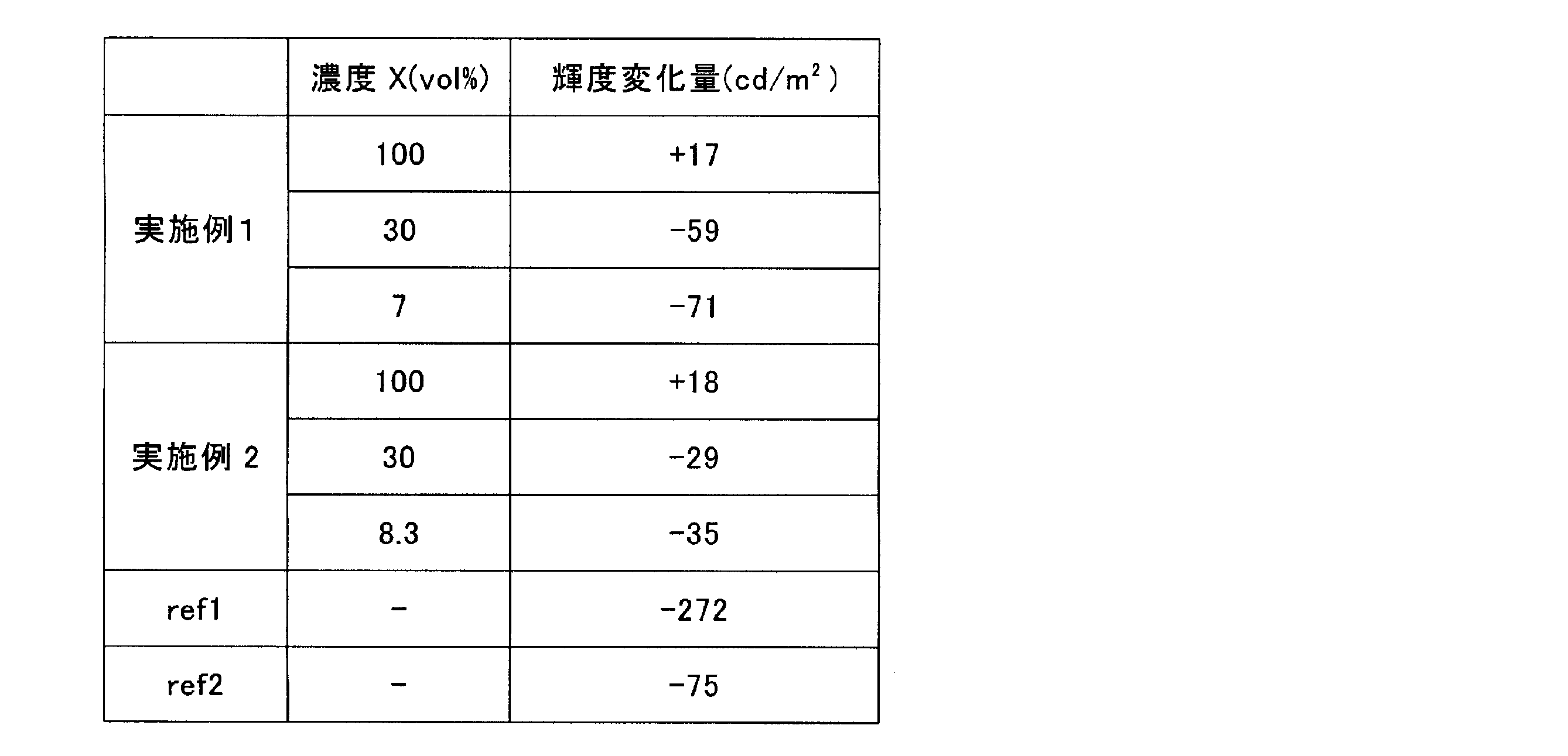
- a plurality of organic EL elements (Example 1) including a block layer were prepared, the characteristics thereof were measured, and the blocking effect of the n-type dopant block layer on alkali metal ions (Cs) was evaluated.
- copper phthalocyanine CuPc is formed in a thickness of 25 nm as a hole injection layer in order by vacuum deposition on a glass substrate on which a transparent electrode ITO is formed as an anode
- NPB N, N′-Bis (naphthalen-1-yl) -N, N′-bis (phenyl) -benzidine is formed with a thickness of 45 nm
- an Alq3 Tris (8-hydroxyquinolinato) aluminum ( III) “Light atoms (Al: 27) were formed to a thickness of 30 nm.
- Example 1 a plurality of precursors formed in the same manner up to the organic light emitting layer Alq3 were prepared, and the concentration was increased by co-evaporation on each organic light emitting layer.
- Example 1 more An organic EL device was fabricated, and the device structure is as follows.
- the inside of () is a film thickness (nm).
- a plurality of organic EL elements were produced.
- a plurality of organic EL elements of Comparative Examples 1 and 2 were fabricated in the same manner except that the n-type dopant block layer was omitted and the light emitting layer thickness was changed to 30 nm and 40 nm.
- the device structures of Comparative Examples 1 and 2 were ITO / hole injection layer / hole transport layer / light emitting layer / electron transport layer / Al in this order: ITO / CuPc (25) / NPB (45) / Alq3 (30) / 1.7 vol% -Cs 2 MoO 4 : NBphen (30) / Al (ref1) and ITO / CuPc (25) / NPB (45) / Alq3 (40) /1.7 vol% -Cs 2 MoO 4 : NBphen ( 20) / Al (ref2).
- the inside of () is a film thickness (nm).
- Examples 1 and 2 and Comparative Examples 1 and 2 were driven under conditions of a current density of 7.5 mA / cm 2 under a high temperature storage environment (85 ° C., 100 hours), respectively.
- the change in luminance (cd / m 2 ) with luminance was measured.
- Table 1 below shows the heavy atom compound concentration of the n-type dopant block layer, the luminance change amount, and the correlation experiment results.
- the evaluation is generally practical from the rule of thumb when the amount of change in luminance can maintain a value of ⁇ 10 cd / m 2 or more. Therefore, when the concentration of heavy atom compound in the n-type dopant block layer is 100 vol%, the change in luminance is It can be seen that it can be maintained.
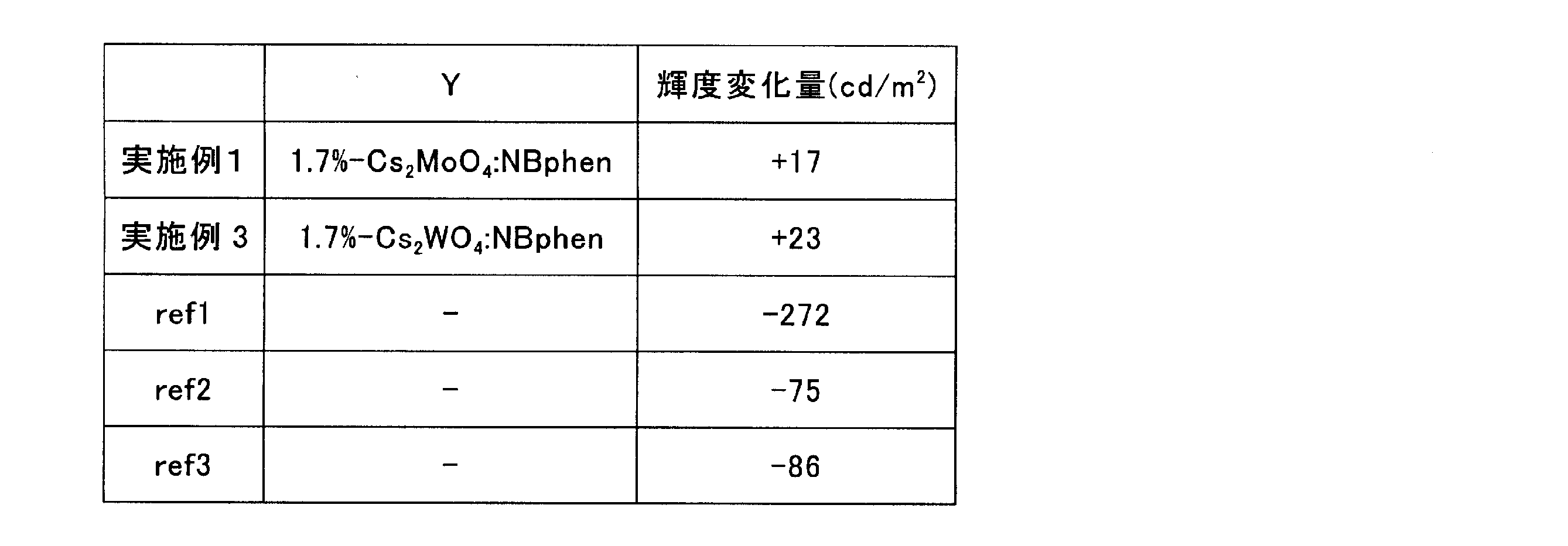
- Example 3-- As Example 3, a device using an n-type dopant-containing electron transport layer containing another n-type dopant was prepared.
- Example 1 as a 100 vol% n-type dopant block layer of Ir (ppy) 3, the n-type dopant Cs 2 MoO 4 molybdate in the n-type dopant-containing electron transport layer was replaced with Cs 2 WO 4 tungstate. A plurality of organic EL elements of Example 3 were produced in the same manner except for the above.
- the device structure of Example 3 is ITO / Hole injection layer / Hole transport layer / light emitting layer / n-type dopant block layer / electron transport layer / Al in this order: ITO / CuPc (25) / NPB (40) / 9 vol% ⁇ Ir (ppy) 3: TRZ ( 40) /1.7vol%-Cs 2 WO 4: a NBphen (20) / Al.
- the inside of () is a film thickness (nm).
- Comparative Example 3 an organic EL device was produced in the same manner as Comparative Example 2 except that tungstate was used instead of the molybdate of the n-type dopant of the electron transport layer.
- the element structure of Comparative Example 3 is ITO / CuPc (25) / NPB (45) / Alq3 (40) /1.7 vol% -Cs 2 WO 4 : NBphen (20) / Al (ref3).
- the inside of () is a film thickness (nm).
- Example 3 For Comparative Example 1, 2, 3, high-temperature storage environment (85 ° C., 100 hours) under a current density 7.5 mA / cm 2, and respectively driven under the condition of 7.5 mA / cm 2 The change in luminance (cd / m 2 ) between initial luminance and luminance after 100 hours was measured.
- Y represents the n-type dopant-containing electron transport layer when the laminated structure of Example 1 and Example 3 is expressed as ITO / CuPc / NPB / 9 vol% -Ir (ppy) 3: TRZ / Y / Al. Ingredients are shown.
- n-type dopant-containing electron transport layer 1.7 vol% -Cs 2 WO 4 : NBphen
- the other n-type dopant-containing electron transport layer 1.7 vol% -Cs 2 WO 4 : NBphen
- n-type dopant block layer was also used as the light emitting layer, that is, integrated to increase the film thickness as an n-type dopant block light emitting layer was produced.
- a plurality of organic EL devices including the n-type dopant block light-emitting layer were prepared, the characteristics thereof were measured, and the blocking effect of the n-type dopant block layer on the metal ions (Cs) was evaluated.
- a transparent electrode ITO is formed as an anode
- copper phthalocyanine CuPc is formed in a thickness of 25 nm as a hole injection layer in order by vacuum deposition
- NPB as a hole transport layer is formed thereon with a thickness of 40 nm.
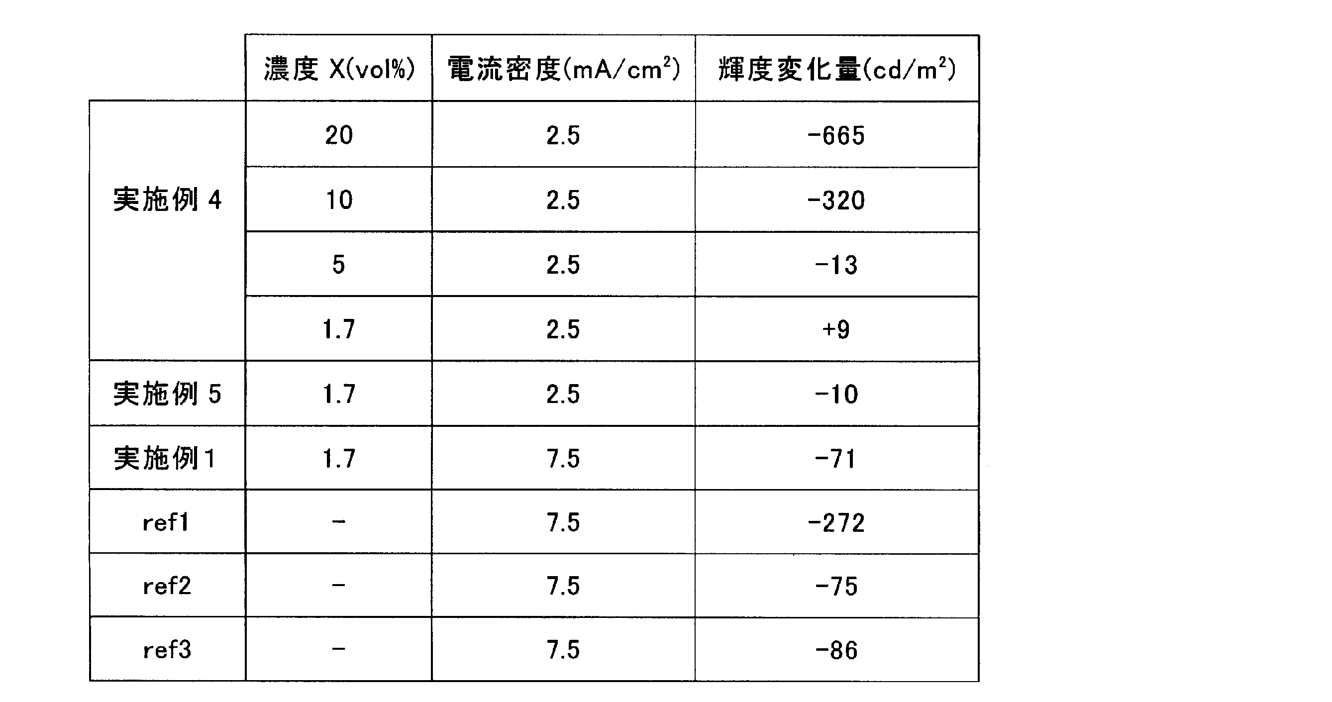
- a TRZ n-type dopant block light-emitting layer containing a heavy atom compound Ir (ppy) 3 at a concentration of 9 vol% was formed to a thickness of 40 nm by co-evaporation.
- a plurality of precursors formed in the same manner up to the n-type dopant block light emitting layer are prepared, and the n-type dopant Cs is formed on each light emitting layer by co-evaporation at a concentration of 1.7 vol%, 5 vol%, 10 vol%, and 20 vol%.
- An electron transport layer of NBphen containing 2 MoO 4 was individually formed so as to have a thickness of 20 nm, and a cathode Al was formed thereon with a predetermined thickness. In this way, a plurality of organic EL elements of Example 4 were produced.
- the element structure is as follows.
- Example 5 An organic EL device of Example 5 was produced in the same manner as in Example 4 , except that the electron transport layer containing Cs 2 MoO 4 was replaced with an electron transport layer containing 1.7 vol% of Cs 2 WO 4 . .
- the device structure of Example 5 is ITO / CuPc (25) / NPB (40) / 9 vol% -Ir (in order of ITO / hole injection layer / hole transport layer / n-type dopant block light emitting layer / electron transport layer / Al).
- ppy) 3 TRZ (40) /1.7vol%-Cs 2 WO 4: a NBphen (20) / Al.
- the inside of () is a film thickness (nm).
- Example 4 each was driven under the condition of a current density of 2.5 mA / cm 2 under a high-temperature storage environment (85 ° C., 100 hours), and the luminance (cd / m) between the initial luminance and the luminance after 100 hours. The change in 2 ) was measured.
- the thickness of the n-type dopant block light-emitting layer is increased, luminance degradation can be prevented even if the n-type dopant containing metal atoms or ions contained in the electron transport layer is increased.
- the current value is set high because the light emission intensity is weak. Further, it can be seen that can suppress the n-type dopant-containing electron-transporting layer of Cs 2 MoO 4 deteriorates below a concentration 10 vol%.
- the volume content concentration of the heavy atom compound in the n-type dopant block layer is equal to or higher than the volume content concentration of the n-type dopant in the n-type dopant-containing electron transport layer. If the conditions are maintained, the effect of preventing diffusion of the n-type dopant can be expected.
- the concentration of the heavy atom compound is selected from 0.1 vol% to 100 vol%, and the concentration of the n-type dopant is selected from 0.1 vol% to 100 vol%.
- the organic EL element was demonstrated in the said Example, as an organic semiconductor element, for example, in this organic solar cell in which a some organic-semiconductor layer contains at least one of a light collection layer, an electron carrying layer, and a hole transport layer, for example.
- the invention is applicable.
- the structure having an n-type dopant block layer made of an organic compound that obstructs the passage of the electron donating material in contact with the electron injection layer also exhibits the life extension effect and moisture resistance effect similar to those in the above examples.
Abstract
Description
2 陽極
3 ホール注入層
4 ホール輸送層
5 発光層
6 n型ドーパントブロック層
7 n型ドーパント含有電子輸送層
7A 電子注入層
8 陰極
56 n型ドーパントブロック発光層
基板1のガラスの透明材料の他としては、ポリスチレン等のプラスチック材料といった半透明材料の他に、シリコンやAl等の不透明な材料、フェノール樹脂等の熱硬化性樹脂、ポリカーボネート等の熱可塑性樹脂等を用いることができる。
ホール注入層3、ホール輸送層4、発光層5、n型ドーパントブロック層6並びにn型ドーパント含有電子輸送層7の主成分を構成する有機半導体層は、電荷輸送性(ホール及び/又は電子の移動性)を有する有機化合物を利用する。
n型ドーパント含有電子輸送層の主成分の電子輸送性を有する有機化合物(上記の電子輸送性有機化合物から選択される)へ混合される電子供与性材料であるn型ドーパントは、Li,Na,K,Rb,Csなどのアルカリ金属や、Be,Mg,Ca,Baなどのアルカリ土類金属や、Sc,Y,Yb,Eu,Sm,Ceなどの希土類金属や、これらのハロゲン塩(LiF,CsFなど)や、これらの酸化物塩(Cs2MoO4,Cs2WO4)や、これらの有機化合物(BLiq4,CsTPBなど)、それらの化合物であれば特に限定はない。特に、仕事関数が4.0eV以下の金属が好適に使用でき、具体例としてCs、Li、Na、K、Be、Mg、Ca、Sr、Ba、Y、La、Mg、Sm、Gd、Yb、又はそれらの化合物等が挙げられる。
発明者は、n型ドーパント含有電子輸送層から隣接層へのアルカリ金属化合物などのn型ドーパント(金属又はそのイオン)の拡散防止のためにn型ドーパントブロック層を提案する。n型ドーパントブロック層に重原子化合物を含ませることにより内部重原子効果を発揮させるのである。
第1成分の電子輸送性を有する有機化合物のNBphen=2,9-Bis(naphthalen-2-yl)-4,7-diphenyl-1,10-phenanthrolineに、電子供与性のアルカリ金属Csを含むn型ドーパントCs2MoO4が第2成分として混合されたn型ドーパント含有電子輸送層と、第3成分の電子輸送性を有する有機化合物TRZ=1,3,5-Triazine derivativesに、79以上の原子量を持つ少なくとも1種の重原子を含有する重原子化合物Ir(ppy)3=Tris(2-phenylpyridine)iridium(III) 「重原子(Ir:192)」が第4成分として混合されたn型ドーパントブロック層と、を含む複数の有機EL素子(実施例1)を作製し、その特性を測定し、アルカリ金属イオン(Cs)に対するn型ドーパントブロック層のブロック効果を評価した。
実施例3として、他のn型ドーパントを含むn型ドーパント含有電子輸送層を用いた素子を作成した。
他の実施例として、n型ドーパントブロック層を発光層と兼用、すなわち、一体化しn型ドーパントブロック発光層として膜厚を増加させた素子を作成した。
Claims (12)
- 対向する1対の陽極及び陰極の間に積層配置されかつ有機発光層を含む複数の有機半導体層を備え、第1成分の電子輸送性を有する有機化合物に、電子供与性の金属原子又はそのイオンを含むn型ドーパントが第2成分として混合されたn型ドーパント含有電子輸送層を前記陰極及び前記有機発光層間に有する有機電界発光素子であって、79以上の原子量を持つ少なくとも1種の重原子を含有する重原子化合物を含みかつ前記n型ドーパント含有電子輸送層の界面に接するn型ドーパントブロック層を有することを特徴とする有機電界発光素子。
- 前記n型ドーパントブロック層は、第3成分の電子輸送性を有する有機化合物に前記重原子化合物が第4成分として混合されていることを特徴とする請求項1に記載の有機電界発光素子。
- 前記n型ドーパント含有電子輸送層の前記n型ドーパントはアルカリ金属、アルカリ土類金属又はそれらの化合物であることを特徴とする請求項1~2のいずれか1に記載の有機電界発光素子。
- 前記n型ドーパントブロック層は、前記有機発光層の界面に接していることを特徴とする請求項1~3のいずれか1に記載の有機電界発光素子。
- 前記n型ドーパントブロック層は、前記有機発光層と一体となっていることを特徴とする請求項1~4のいずれか1に記載の有機電界発光素子。
- 前記n型ドーパント含有電子輸送層の前記陰極側に電子注入層が配置されていることを特徴とする請求項1~5のいずれか1に記載の有機電界発光素子。
- 前記n型ドーパントブロック層における前記重原子化合物の体積含有量濃度は、前記n型ドーパント含有電子輸送層における前記n型ドーパントの体積含有量濃度以上であることを特徴とする請求項1~6のいずれか1に記載の有機電界発光素子。
- 前記重原子化合物の濃度は、0.1vol%~100vol%であることを特徴とする請求項1~7のいずれか1に記載の有機電界発光素子。
- 前記n型ドーパントの濃度は、0.1vol%~100vol%であることを特徴とする請求項1~7のいずれか1に記載の有機電界発光素子。
- 前記重原子がIr、Pt,Os,Re,Au,W,Ru,Hf,Eu,Tb,等の重原子、希土類金属から構成する重原子化合物であることを特徴とする請求項1~9のいずれか1に記載の有機電界発光素子。
- 前記金属原子又はそのイオンは、Li,Na,K,Rb,Cs,Be,Mg,Ca,Ba,Sc,Y,Yb,Eu,Sm,Ceから選択されたものであることを特徴とする請求項1~10のいずれか1に記載の有機電界発光素子。
- 前記陽極及び陰極のどちらか片方の電極が半透明、又は透明、又は前記陽極及び陰極が透明であることを特徴とする請求項1~11のいずれか1に記載の有機電界発光素子。
Priority Applications (5)
| Application Number | Priority Date | Filing Date | Title |
|---|---|---|---|
| JP2010523660A JP5090534B2 (ja) | 2008-08-04 | 2008-08-04 | 有機電界発光素子 |
| US13/057,343 US8436345B2 (en) | 2008-08-04 | 2008-08-04 | Organic electroluminescence device |
| PCT/JP2008/063962 WO2010016101A1 (ja) | 2008-08-04 | 2008-08-04 | 有機電界発光素子 |
| KR1020117002232A KR101254167B1 (ko) | 2008-08-04 | 2008-08-04 | 유기 전계발광 소자 |
| EP08792166.4A EP2315290B1 (en) | 2008-08-04 | 2008-08-04 | Organic electroluminescent element |
Applications Claiming Priority (1)
| Application Number | Priority Date | Filing Date | Title |
|---|---|---|---|
| PCT/JP2008/063962 WO2010016101A1 (ja) | 2008-08-04 | 2008-08-04 | 有機電界発光素子 |
Publications (1)
| Publication Number | Publication Date |
|---|---|
| WO2010016101A1 true WO2010016101A1 (ja) | 2010-02-11 |
Family
ID=41663331
Family Applications (1)
| Application Number | Title | Priority Date | Filing Date |
|---|---|---|---|
| PCT/JP2008/063962 WO2010016101A1 (ja) | 2008-08-04 | 2008-08-04 | 有機電界発光素子 |
Country Status (5)
| Country | Link |
|---|---|
| US (1) | US8436345B2 (ja) |
| EP (1) | EP2315290B1 (ja) |
| JP (1) | JP5090534B2 (ja) |
| KR (1) | KR101254167B1 (ja) |
| WO (1) | WO2010016101A1 (ja) |
Cited By (8)
| Publication number | Priority date | Publication date | Assignee | Title |
|---|---|---|---|---|
| CN102097601A (zh) * | 2011-01-05 | 2011-06-15 | 河北工业大学 | N型掺杂薄膜的有机发光二极管 |
| WO2012023177A1 (ja) * | 2010-08-17 | 2012-02-23 | パイオニア株式会社 | 有機発光素子 |
| WO2013171872A1 (ja) * | 2012-05-17 | 2013-11-21 | パイオニア株式会社 | 有機el発光パネル及び発光装置 |
| JP2014503979A (ja) * | 2010-11-22 | 2014-02-13 | 出光興産株式会社 | 有機エレクトロルミネッセンス素子 |
| JP2014524142A (ja) * | 2011-06-22 | 2014-09-18 | ノヴァレッド・アクチエンゲゼルシャフト | 電子装置および化合物 |
| US9324950B2 (en) | 2010-11-22 | 2016-04-26 | Idemitsu Kosan Co., Ltd. | Organic electroluminescence device |
| US9601696B2 (en) | 2011-03-28 | 2017-03-21 | Sumitomo Chemical Company, Limited | Electroluminescent composition and electric device with high brightness |
| US11758749B2 (en) | 2018-10-26 | 2023-09-12 | Joled Inc. | Organic EL element having one functional layer with NaF and the other functional layer with Yb |
Families Citing this family (9)
| Publication number | Priority date | Publication date | Assignee | Title |
|---|---|---|---|---|
| US8883323B2 (en) | 2010-11-22 | 2014-11-11 | Idemitsu Kosan Co., Ltd. | Organic electroluminescence device |
| KR101671343B1 (ko) | 2012-05-22 | 2016-11-02 | 삼성디스플레이 주식회사 | 유기 발광 소자 및 그 제조방법 |
| US10374187B2 (en) | 2012-05-22 | 2019-08-06 | Samsung Display Co., Ltd. | Organic light-emitting device and method of producing the same |
| KR101441963B1 (ko) * | 2012-06-14 | 2014-09-24 | 서울대학교산학협력단 | 양면 발광형 유기 발광 소자 및 그 제조 방법 |
| JP2014063829A (ja) * | 2012-09-20 | 2014-04-10 | Samsung Display Co Ltd | 有機el表示装置 |
| KR102356696B1 (ko) * | 2015-07-03 | 2022-01-26 | 삼성전자주식회사 | 유기 광전 소자 및 이미지 센서 |
| EP3184602B1 (en) * | 2015-12-23 | 2018-07-04 | Avantama AG | Luminescent component |
| KR102503845B1 (ko) * | 2016-04-20 | 2023-02-27 | 삼성디스플레이 주식회사 | 유기발광소자 및 이를 포함하는 유기발광 표시패널 |
| CN107799571B (zh) * | 2017-10-12 | 2020-10-09 | 武汉华星光电半导体显示技术有限公司 | 有机发光二极管器件及显示装置 |
Citations (5)
| Publication number | Priority date | Publication date | Assignee | Title |
|---|---|---|---|---|
| JP2005123094A (ja) * | 2003-10-17 | 2005-05-12 | Junji Kido | 有機エレクトロルミネッセント素子及びその製造方法 |
| JP2006173619A (ja) * | 2004-12-16 | 2006-06-29 | Au Optronics Corp | 有機発光ダイオード及びその製造方法 |
| JP2007088015A (ja) | 2005-09-20 | 2007-04-05 | Konica Minolta Holdings Inc | 有機エレクトロルミネッセンス素子、および有機レクトロルミネッセンス素子の製造方法 |
| JP2007180277A (ja) | 2005-12-28 | 2007-07-12 | Konica Minolta Holdings Inc | 有機エレクトロルミネッセンス素子、表示装置及び照明装置 |
| JP2008098475A (ja) * | 2006-10-13 | 2008-04-24 | Fuji Electric Holdings Co Ltd | 有機発光素子の構造 |
Family Cites Families (3)
| Publication number | Priority date | Publication date | Assignee | Title |
|---|---|---|---|---|
| WO2006000020A1 (en) | 2004-06-29 | 2006-01-05 | European Nickel Plc | Improved leaching of base metals |
| JP2008509565A (ja) * | 2004-08-13 | 2008-03-27 | ノヴァレッド・アクチエンゲゼルシャフト | 発光成分用積層体 |
| GB2439013B (en) | 2005-03-28 | 2010-10-06 | Konica Minolta Holdings Inc | Organic electroluminescent element, display and illuminator |
-
2008
- 2008-08-04 US US13/057,343 patent/US8436345B2/en active Active
- 2008-08-04 EP EP08792166.4A patent/EP2315290B1/en active Active
- 2008-08-04 KR KR1020117002232A patent/KR101254167B1/ko active IP Right Grant
- 2008-08-04 JP JP2010523660A patent/JP5090534B2/ja active Active
- 2008-08-04 WO PCT/JP2008/063962 patent/WO2010016101A1/ja active Application Filing
Patent Citations (5)
| Publication number | Priority date | Publication date | Assignee | Title |
|---|---|---|---|---|
| JP2005123094A (ja) * | 2003-10-17 | 2005-05-12 | Junji Kido | 有機エレクトロルミネッセント素子及びその製造方法 |
| JP2006173619A (ja) * | 2004-12-16 | 2006-06-29 | Au Optronics Corp | 有機発光ダイオード及びその製造方法 |
| JP2007088015A (ja) | 2005-09-20 | 2007-04-05 | Konica Minolta Holdings Inc | 有機エレクトロルミネッセンス素子、および有機レクトロルミネッセンス素子の製造方法 |
| JP2007180277A (ja) | 2005-12-28 | 2007-07-12 | Konica Minolta Holdings Inc | 有機エレクトロルミネッセンス素子、表示装置及び照明装置 |
| JP2008098475A (ja) * | 2006-10-13 | 2008-04-24 | Fuji Electric Holdings Co Ltd | 有機発光素子の構造 |
Non-Patent Citations (2)
| Title |
|---|
| "Photochemical Dimerization of Acephenanthrylene and the Heavy Atom Effect", J. ORG. CHEM., vol. 65, no. 2, 2000, pages 450 - 452 |
| See also references of EP2315290A4 |
Cited By (10)
| Publication number | Priority date | Publication date | Assignee | Title |
|---|---|---|---|---|
| WO2012023177A1 (ja) * | 2010-08-17 | 2012-02-23 | パイオニア株式会社 | 有機発光素子 |
| JPWO2012023177A1 (ja) * | 2010-08-17 | 2013-10-28 | パイオニア株式会社 | 有機発光素子 |
| JP2014503979A (ja) * | 2010-11-22 | 2014-02-13 | 出光興産株式会社 | 有機エレクトロルミネッセンス素子 |
| KR101482829B1 (ko) * | 2010-11-22 | 2015-01-14 | 이데미쓰 고산 가부시키가이샤 | 유기 일렉트로루미네선스 소자 |
| US9324950B2 (en) | 2010-11-22 | 2016-04-26 | Idemitsu Kosan Co., Ltd. | Organic electroluminescence device |
| CN102097601A (zh) * | 2011-01-05 | 2011-06-15 | 河北工业大学 | N型掺杂薄膜的有机发光二极管 |
| US9601696B2 (en) | 2011-03-28 | 2017-03-21 | Sumitomo Chemical Company, Limited | Electroluminescent composition and electric device with high brightness |
| JP2014524142A (ja) * | 2011-06-22 | 2014-09-18 | ノヴァレッド・アクチエンゲゼルシャフト | 電子装置および化合物 |
| WO2013171872A1 (ja) * | 2012-05-17 | 2013-11-21 | パイオニア株式会社 | 有機el発光パネル及び発光装置 |
| US11758749B2 (en) | 2018-10-26 | 2023-09-12 | Joled Inc. | Organic EL element having one functional layer with NaF and the other functional layer with Yb |
Also Published As
| Publication number | Publication date |
|---|---|
| JPWO2010016101A1 (ja) | 2012-01-12 |
| EP2315290A1 (en) | 2011-04-27 |
| EP2315290B1 (en) | 2016-03-16 |
| KR20110036096A (ko) | 2011-04-06 |
| JP5090534B2 (ja) | 2012-12-05 |
| KR101254167B1 (ko) | 2013-04-18 |
| EP2315290A4 (en) | 2012-01-25 |
| US8436345B2 (en) | 2013-05-07 |
| US20110169045A1 (en) | 2011-07-14 |
Similar Documents
| Publication | Publication Date | Title |
|---|---|---|
| JP5090534B2 (ja) | 有機電界発光素子 | |
| JP5216104B2 (ja) | 有機電界発光素子 | |
| JP4939284B2 (ja) | 有機エレクトロルミネッセント素子 | |
| JP4486713B2 (ja) | 有機エレクトロルミネッセント素子 | |
| KR100641880B1 (ko) | 유기전기장발광성소자 | |
| JP4514841B2 (ja) | 有機エレクトロルミネッセント素子 | |
| JP4824848B2 (ja) | 有機エレクトロルミネッセント素子、有機エレクトロルミネッセント素子群及びその発光スペクトルの特定方法 | |
| JP4729154B2 (ja) | 有機エレクトロルミネッセント素子、有機エレクトロルミネッセント素子群及びその発光スペクトルの制御方法 | |
| JP4505067B2 (ja) | 有機エレクトロルミネッセント素子 | |
| US6013384A (en) | Organic electroluminescent devices | |
| KR101688317B1 (ko) | 저전압 구동 유기발광소자 및 이의 제조 방법 | |
| JP2004079413A (ja) | 有機エレクトロルミネッセント素子 | |
| WO2009110075A1 (ja) | 有機半導体素子 | |
| JP5456120B2 (ja) | 有機電界発光素子 | |
| WO2009107541A1 (ja) | 有機電界発光素子 | |
| JPWO2004052057A1 (ja) | 有機電界発光素子 | |
| JP4825296B2 (ja) | 有機エレクトロルミネッセント素子 | |
| JP4820902B2 (ja) | 有機エレクトロルミネッセント素子及びその発光スペクトルの制御方法 | |
| JP2004079414A (ja) | 有機エレクトロルミネッセント素子 | |
| Chang et al. | 17.4: Highly Power Efficient Organic Light‐Emitting Diodes with a Novel P‐Doping Layer |
Legal Events
| Date | Code | Title | Description |
|---|---|---|---|
| 121 | Ep: the epo has been informed by wipo that ep was designated in this application |
Ref document number: 08792166 Country of ref document: EP Kind code of ref document: A1 |
|
| WWE | Wipo information: entry into national phase |
Ref document number: 2010523660 Country of ref document: JP |
|
| ENP | Entry into the national phase |
Ref document number: 20117002232 Country of ref document: KR Kind code of ref document: A |
|
| WWE | Wipo information: entry into national phase |
Ref document number: 2008792166 Country of ref document: EP |
|
| NENP | Non-entry into the national phase |
Ref country code: DE |
|
| WWE | Wipo information: entry into national phase |
Ref document number: 13057343 Country of ref document: US |