WO2009157341A1 - スパッタリング装置及びその制御用プログラムを記録した記録媒体 - Google Patents
スパッタリング装置及びその制御用プログラムを記録した記録媒体 Download PDFInfo
- Publication number
- WO2009157341A1 WO2009157341A1 PCT/JP2009/060911 JP2009060911W WO2009157341A1 WO 2009157341 A1 WO2009157341 A1 WO 2009157341A1 JP 2009060911 W JP2009060911 W JP 2009060911W WO 2009157341 A1 WO2009157341 A1 WO 2009157341A1
- Authority
- WO
- WIPO (PCT)
- Prior art keywords
- substrate
- support holder
- substrate support
- deposition
- rotations
- Prior art date
- Legal status (The legal status is an assumption and is not a legal conclusion. Google has not performed a legal analysis and makes no representation as to the accuracy of the status listed.)
- Ceased
Links
Images





Classifications
-
- C—CHEMISTRY; METALLURGY
- C23—COATING METALLIC MATERIAL; COATING MATERIAL WITH METALLIC MATERIAL; CHEMICAL SURFACE TREATMENT; DIFFUSION TREATMENT OF METALLIC MATERIAL; COATING BY VACUUM EVAPORATION, BY SPUTTERING, BY ION IMPLANTATION OR BY CHEMICAL VAPOUR DEPOSITION, IN GENERAL; INHIBITING CORROSION OF METALLIC MATERIAL OR INCRUSTATION IN GENERAL
- C23C—COATING METALLIC MATERIAL; COATING MATERIAL WITH METALLIC MATERIAL; SURFACE TREATMENT OF METALLIC MATERIAL BY DIFFUSION INTO THE SURFACE, BY CHEMICAL CONVERSION OR SUBSTITUTION; COATING BY VACUUM EVAPORATION, BY SPUTTERING, BY ION IMPLANTATION OR BY CHEMICAL VAPOUR DEPOSITION, IN GENERAL
- C23C14/00—Coating by vacuum evaporation, by sputtering or by ion implantation of the coating forming material
- C23C14/22—Coating by vacuum evaporation, by sputtering or by ion implantation of the coating forming material characterised by the process of coating
- C23C14/34—Sputtering
- C23C14/3492—Variation of parameters during sputtering
-
- C—CHEMISTRY; METALLURGY
- C23—COATING METALLIC MATERIAL; COATING MATERIAL WITH METALLIC MATERIAL; CHEMICAL SURFACE TREATMENT; DIFFUSION TREATMENT OF METALLIC MATERIAL; COATING BY VACUUM EVAPORATION, BY SPUTTERING, BY ION IMPLANTATION OR BY CHEMICAL VAPOUR DEPOSITION, IN GENERAL; INHIBITING CORROSION OF METALLIC MATERIAL OR INCRUSTATION IN GENERAL
- C23C—COATING METALLIC MATERIAL; COATING MATERIAL WITH METALLIC MATERIAL; SURFACE TREATMENT OF METALLIC MATERIAL BY DIFFUSION INTO THE SURFACE, BY CHEMICAL CONVERSION OR SUBSTITUTION; COATING BY VACUUM EVAPORATION, BY SPUTTERING, BY ION IMPLANTATION OR BY CHEMICAL VAPOUR DEPOSITION, IN GENERAL
- C23C14/00—Coating by vacuum evaporation, by sputtering or by ion implantation of the coating forming material
- C23C14/22—Coating by vacuum evaporation, by sputtering or by ion implantation of the coating forming material characterised by the process of coating
- C23C14/225—Oblique incidence of vaporised material on substrate
-
- C—CHEMISTRY; METALLURGY
- C23—COATING METALLIC MATERIAL; COATING MATERIAL WITH METALLIC MATERIAL; CHEMICAL SURFACE TREATMENT; DIFFUSION TREATMENT OF METALLIC MATERIAL; COATING BY VACUUM EVAPORATION, BY SPUTTERING, BY ION IMPLANTATION OR BY CHEMICAL VAPOUR DEPOSITION, IN GENERAL; INHIBITING CORROSION OF METALLIC MATERIAL OR INCRUSTATION IN GENERAL
- C23C—COATING METALLIC MATERIAL; COATING MATERIAL WITH METALLIC MATERIAL; SURFACE TREATMENT OF METALLIC MATERIAL BY DIFFUSION INTO THE SURFACE, BY CHEMICAL CONVERSION OR SUBSTITUTION; COATING BY VACUUM EVAPORATION, BY SPUTTERING, BY ION IMPLANTATION OR BY CHEMICAL VAPOUR DEPOSITION, IN GENERAL
- C23C14/00—Coating by vacuum evaporation, by sputtering or by ion implantation of the coating forming material
- C23C14/22—Coating by vacuum evaporation, by sputtering or by ion implantation of the coating forming material characterised by the process of coating
- C23C14/34—Sputtering
- C23C14/3407—Cathode assembly for sputtering apparatus, e.g. Target
-
- C—CHEMISTRY; METALLURGY
- C23—COATING METALLIC MATERIAL; COATING MATERIAL WITH METALLIC MATERIAL; CHEMICAL SURFACE TREATMENT; DIFFUSION TREATMENT OF METALLIC MATERIAL; COATING BY VACUUM EVAPORATION, BY SPUTTERING, BY ION IMPLANTATION OR BY CHEMICAL VAPOUR DEPOSITION, IN GENERAL; INHIBITING CORROSION OF METALLIC MATERIAL OR INCRUSTATION IN GENERAL
- C23C—COATING METALLIC MATERIAL; COATING MATERIAL WITH METALLIC MATERIAL; SURFACE TREATMENT OF METALLIC MATERIAL BY DIFFUSION INTO THE SURFACE, BY CHEMICAL CONVERSION OR SUBSTITUTION; COATING BY VACUUM EVAPORATION, BY SPUTTERING, BY ION IMPLANTATION OR BY CHEMICAL VAPOUR DEPOSITION, IN GENERAL
- C23C14/00—Coating by vacuum evaporation, by sputtering or by ion implantation of the coating forming material
- C23C14/22—Coating by vacuum evaporation, by sputtering or by ion implantation of the coating forming material characterised by the process of coating
- C23C14/54—Controlling or regulating the coating process
Definitions
- the present invention relates to a sputtering apparatus used for depositing a film forming material on a film formation surface of a substrate and a program used for its drive control in the process of manufacturing an electronic device such as a magnetic recording medium, a semiconductor device or a display device.
- the present invention relates to a recording medium recorded.
- an oblique sputtering apparatus in order to deposit a film forming material uniformly on a film formation surface of a substrate using a target smaller than the substrate.
- the sputtering cathode supporting the target and the substrate support holder supporting the substrate are arranged such that the surface of the target is inclined with respect to the deposition surface of the substrate.
- Deposition of the film forming material is performed by flying sputtered particles from the oblique direction to the film formation surface of the substrate while rotating the substrate support holder and rotating the film formation surface of the substrate within a certain plane (for example, Patent Documents 1, 2, 3, 4 and 5).
- deposition of a very small amount of a film-forming material is performed with a sputtering apparatus, as in the case of the film thickness of 10 nm or less, particularly 1 nm or less described above, deposition is performed in a short time of several seconds to several tens of seconds. Will be completed.
- the speed-up limit of the rotation speed of the substrate support holder is about 100 rpm. Therefore, the number of rotations of the substrate support holder stops at a few tens of rotations at a deposition time of several seconds to several tens of seconds, and even if it is intended to improve the uniformity of the deposition amount by increasing the number of rotations, the number of rotations exceeds this It is difficult to increase.
- the sputtering apparatus has a sputtering cathode for supporting a target, and a substrate support holder for supporting a substrate.
- the sputtering cathode and the substrate support holder are provided such that a perpendicular passing through the center point of the target and a perpendicular passing through the center point of the substrate among the perpendiculars to the plane including the deposition surface of the substrate do not match. It is done. Specifically, in the case where the deposition surface of the substrate and the surface of the target are parallel and the positions of the central points of the two are shifted, the deposition surface of the substrate and the surface of the target are not In parallel, there is a case where the position of the center point of both is shifted.
- the sputtering apparatus includes power supply means for supplying power to the sputtering cathode, and the deposition time T is from the start of power supply from the power supply means to the sputtering cathode to the end of power supply.
- the preferred embodiment of the invention is that
- the sputtering apparatus includes power supply means for supplying power to the sputtering cathode, and a shutter capable of opening and closing is provided between the sputtering cathode and the substrate support holder.
- a preferred embodiment includes that the deposition time T is a time during which power is supplied from the power supply means to the sputtering cathode and the shutter is open.
- a recording medium has a sputtering cathode for supporting a target, and a substrate support holder for supporting a substrate, and the perpendicular line to the plane including the deposition surface of the substrate includes the target
- the sputtering cathode and the substrate support holder are provided such that a vertical line passing through the central point and a vertical line passing through the central point of the substrate do not match, and the substrate support holder is a film on the substrate on which the substrate is deposited.
- the deposition time T is 1 to 400 seconds
- the total integer rotation speed N is 1 to 100
- the rotation speed V of the substrate support holder is 0.016 to 3.
- the preferred embodiments include 5 rps and a fractional rotation number ⁇ of 0.2 to 0.8.
- a deposited film of 10 nm or less in film thickness such as a gate insulating film or a multilayer magnetic film, in particular, a deposited film of 1 nm or less in film thickness can be deposited uniformly over most regions of the substrate.
- the present invention can provide a high-performance semiconductor device and a magnetic memory device such as a TMR (Tunneling Magneto Resistance) device.
- a magnetic memory device such as a TMR (Tunneling Magneto Resistance) device.
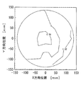
- FIG. 16 is a view showing a distribution of deposition amount of Mg in Example 4. It is a figure which shows deposition amount distribution of Mg in the comparative example 1.
- FIG. 6 is a graph showing the relationship between the deviation angle ⁇ (fractional rotation number ⁇ ) and the uniformity of the deposition amount based on Examples 1 to 4 and Comparative Example 1.
- FIG. 1 is a schematic cross-sectional view showing an example of a sputtering apparatus according to the present invention.
- a sputtering cathode 3 for supporting a target 2 is provided on the ceiling of the vacuum vessel 1. Further, at the center of the bottom surface portion of the vacuum vessel 1, a substrate support holder 6 attached to a rotation shaft 5 rotated by a rotation drive mechanism 4 is disposed. The substrate support holder 6 supports the substrate 7 horizontally, and the rotating shaft 4 is provided perpendicularly to the film formation surface (the surface exposed to the target 2 side) of the substrate 7. Therefore, the substrate 7 can be rotated along with the rotation of the substrate support holder 6 in a state where the deposition surface of the substrate 7 is positioned in a predetermined plane.
- the substrate support holder 6 is rotated at least for a deposition time (deposition time) T (second) which is a time for which sputtered particles from the target 2 are deposited on the deposition surface.
- the rotational speed V (rps) of the substrate support holder 6 is preferably constant during the deposition time T, for ease of control.
- the rotational speed V can also be changed during the deposition time T.
- the initial low speed may be set to the low rotational speed
- the second half may be set to the high rotational speed, or conversely, the initial high speed may be set to the low rotational speed.
- the rotational speed V of the substrate support holder 6 can be changed during the deposition time T at a rate of a linear function or a quadratic function.
- the sputtering cathode 3 and the substrate support holder 6 are provided such that the surface of the target 2 (the surface exposed to the substrate 7 side) is inclined with respect to the film formation surface of the substrate 7. Therefore, sputtered particles traveling from the target 2 to the film formation surface of the substrate 7 are deposited by being obliquely incident on the film formation surface.
- the sputtering cathode 3 is connected to a DC power supply 8 as a power supply unit.
- a predetermined DC power for example, 1 W to 1000 W, preferably 10 W to 750 W
- an RF power supply can be used as a power supply means.
- a shutter 10 that can be opened and closed by a shutter drive mechanism 9 is disposed between the sputtering cathode 3 (target 2) and the substrate support holder 6 (substrate 7).
- a shutter drive mechanism 9 When the shutter 10 is opened, sputtered particles generated from the target 2 can be deposited on the film formation surface of the substrate 7.
- the shutter 10 when the shutter 10 is closed, the sputtered particles generated from the target 2 are blocked from flying to the deposition surface of the substrate 7 and the deposition of sputtered particles on the deposition surface of the substrate 7 is prevented. .
- the control unit 11 controls the rotation of the substrate support holder 6, the on / off of the DC power source 8, and the opening / closing of the shutter 10.
- the control unit 11 comprises a CPU (central processing unit) 12, a recording medium 13 recording a control program, and an input unit 14.
- a general purpose computer can be used as the control unit 11.
- the recording medium 13 is a medium capable of recording in a state where a program to be described later can be called, and more specifically, a non-volatile memory such as a hard disk, an optical magnetic disk, a flexible disk, a flash memory, or an MRAM used in a general purpose computer (Non -Volatile memory) can be used.
- a keyboard, a mouse, a touch panel, an audio input means, etc. can be used as the input unit 14.
- the CPU 12 receives from the input unit 14 a first digital value for the deposition time T, a second digital value for the total integer rotational speed N of the substrate support holder 6 within the deposition time T, and a second 3 Digital values are input and temporarily recorded here. These digital values may be recorded on the recording medium 13 so that they can be read as needed.
- the CPU 12 of the control unit 11 is connected to the rotation control mechanism 4, the DC power supply 8, and the shutter drive mechanism 9.
- the CPU 12 of the control unit 11 controls the operation of the DC power supply 8 and the shutter drive mechanism 9 at necessary timings, and controls the operation of the rotation control mechanism 4 in accordance with the timings of these drives. Control the velocity V (rps).
- the rotational speed V of the substrate support holder 6 is controlled such that the total number of rotations X of the substrate holder 6 at the deposition time T is not an integer but always has the fractional number of rotations ⁇ . Be done.
- the deposition time T in the present invention is determined from the thickness of the deposited film to be formed on the substrate 7 and the deposition rate of the sputtering apparatus according to the present invention (the deposition thickness per unit time of the deposition material on the substrate 7). It will be determined.
- the deposition rate can be determined by conducting a preliminary film forming experiment under the same conditions as those for forming the deposition film on the substrate 7.
- the total integer number of revolutions N can be arbitrarily selected within a range where an excessive load is not applied to the rotary drive mechanism 4 according to the capability of the rotary drive mechanism 4.
- the fractional rotation number ⁇ is fixed to the total integer rotation number N, and the preliminary film forming experiment in which the rotation number V of the substrate support holder 6 is adjusted to change the fractional rotation number ⁇ is carried out. It can determine by calculating
- the start and end points of the deposition time T may be, for example, the on / off timing of the power supply means (for example, DC power supply 8) to the sputtering cathode 3, the opening / closing timing of the shutter 10, or the on / off timing of the power supply means and the shutter 10 It can be determined as a combination with the open / close timing.
- the power supply means for example, DC power supply 8
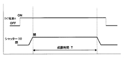
- 2 to 5 respectively show first to fourth timing charts showing the timing of the start point and the end point of the deposition time T, respectively. These timing charts will be described with reference also to FIG.
- the first timing chart of FIG. 2 shows the case where the deposition time T is determined at the timing when the shutter 10 is opened and closed.
- the CPU 12 of the control unit 11 introduces the sputtering gas into the vacuum chamber 1 of the sputtering apparatus, turns on the DC power supply 8 and supplies constant power to the sputtering cathode 3 Discharge is started, and a plasma is generated on the front surface of the target 2.
- the shutter drive mechanism 9 is operated to open the shutter 10.
- the end time of the opening operation of the shutter 10 (when the shutter 10 is fully opened) is the start point of the deposition time T.
- the shutter drive mechanism 9 is operated again to close the shutter 10.
- the start time of the closing operation of the shutter 10 is the end point of the accumulation time T.
- the second timing chart of FIG. 3 shows the case where the deposition time T is determined at the timing of turning on and off the power supply means (for example, the DC power source 8) to the sputtering cathode 3.
- This timing chart can be applied to a device without the shutter 10 or to drive the sputtering device with the shutter 10 always open.
- the time when the CPU 12 of the control unit 11 introduces the sputtering gas into the vacuum chamber 1 of the sputtering apparatus and turns on the DC power supply 8 is the start point of the deposition time T, and then the DC power supply The point at which 8 is turned off is the end point of the deposition time T.
- the third timing chart of FIG. 4 shows a first example in which the deposition time T is determined by a combination of the timing of turning on and off the power supply means (for example, the DC power supply 8) and the timing of opening and closing the shutter 10. is there.
- the start point of the deposition time T in the third timing chart is the same as the start point in the first timing chart.
- the DC power supply 8 is turned off with the shutter 10 kept open, and then the shutter 10 is closed.
- the point at which the DC power supply 8 is turned off is the end point of the deposition time T.
- the fourth timing chart of FIG. 5 shows a second example in which the deposition time T is determined by a combination of the timing of turning on and off the power supply unit (for example, the DC power supply 8) and the timing of opening and closing the shutter 10. is there.
- the CPU 12 of the control unit 11 introduces a sputtering gas into the vacuum chamber 1 of the sputtering apparatus, operates the shutter drive mechanism 9, and opens the shutter 10.
- the DC power supply 8 is turned “on” to supply a constant power to the sputtering cathode 3 to start discharge and generate plasma on the front surface of the target 2.
- the start point of the deposition time T in the fourth timing chart is the time when the DC power supply 8 is turned on. Further, the end point of the deposition time T is the same as the end point in the first timing chart.
- the deposition time T in the present invention is defined as the time for obtaining the required deposited film thickness, but the present invention is particularly effective for forming a thin deposited film, and is effective when the deposited film thickness is 10 nm or less, particularly 1 nm or less. is there. That is, the present invention is effective for forming a deposited film having a short deposition time T, and the deposition time T in the present invention is preferably 1 to 400 seconds, and more preferably 1 to 30 seconds.
- the rotation speed V of the substrate support holder 6 in the present invention may be obtained by a general rotation control mechanism 4 and is preferably in the range of 0.016 to 3.5 rps, more preferably 0.05 to 2 rps. Since very slow rotation requires a special system for the rotation mechanism and control mechanism, it is preferable from the viewpoint of cost to be 0.016 rps or more. And in order to be able to maintain a high vacuum atmosphere with a simple sealing mechanism, it is preferable that rotational speed V is 3.5 rps or less. Moreover, for more stable operation, it is more preferable that the value is 0.05 rps or more.
- the substrate 7 is placed on the substrate support holder 6 and accelerated from the rotation stopped state, and film formation is started after the substrate support holder 6 reaches a desired rotation speed, decelerated after film formation is completed, and stopped Will be returned. For this reason, if the rotational speed is increased, the acceleration / deceleration time of the substrate support holder 6 has a greater effect on the throughput (the number of sheets that can be processed by the apparatus per unit time). It is more preferable that the rotational speed V of the substrate support holder 6 is 2 rps or less, because the maintenance cycle is shortened due to the force applied.
- the total integer number of revolutions N in the present invention is an integer of 1 or more, but is generally in the range of 1 to 100 revolutions, preferably 1 to 50 revolutions.
- the fractional rotation number ⁇ is preferably 0.1 to 0.9, and more preferably 0.2 to 0.8.
- the deviation angle ⁇ refers to the amount of deviation of an angle about the rotation axis 5 that occurs between the start of rotation and the stop of rotation at one point on the substrate support holder 6.
- the material of the target 2 used in the present invention is, for example, Hf (hafnium), Mg (magnesium), La (lanthanum), Zr (zirconium), Ta (tantalum), Ti (titanium), Al (aluminum), Co (co) Metals such as cobalt), Fe (iron), Ni (nickel), Ru (ruthenium), Cu (copper), Pt (platinum), Mn (manganese), Cr (chromium), magnesium oxide, hafnium oxide, lanthanum oxide, Examples of the oxide include oxides such as silicon oxide, tantalum oxide and chromium oxide, and carbides such as silicon carbide. However, the present invention is not limited to these.
- the diameter of the target 2 is preferably set to a value smaller than the diameter of the substrate 7. In a preferred embodiment, the diameter of the target 2 is preferably in the range of 0.1 to 0.9 times, particularly 0.3 to 0.7 times the diameter of the substrate 7.
- a silicon substrate, a gallium arsenide substrate, an AlTiC substrate, a glass substrate, a stainless steel substrate, an aluminum substrate, a plastic substrate or the like can be used, but it is not limited thereto.
- the sputtering cathode 3 and the substrate support holder 6 are provided such that the surface of the target 2 (the surface exposed to the substrate 7 side) is inclined with respect to the film formation surface of the substrate 7 .
- the arrangement of the sputtering cathode 3 and the substrate support holder 6 in the present invention is not limited to this.
- the perpendicular to the plane including the deposition surface of the substrate 7 that passes through the center point of the target 2 does not match the perpendicular to the center point of the substrate.
- the arrangement may be such that the surfaces of the target 2 are parallel.
- FIGS. 6 and 7 are cross-sectional views schematically illustrating the arrangement relationship between the substrate and the target in the present invention, and the same members as those in FIG. 1 are denoted by the same reference numerals.
- 102 is a target
- 103 is a sputtering cathode
- 106 is a substrate support holder
- 107 is a substrate
- a is a perpendicular passing through the center o of the substrate 107 among the perpendiculars to the plane including the deposition surface of the substrate 107 a)
- b are perpendiculars (substrate perpendicular b) passing through the center p of the target 102
- the shift amount l is the distance between the substrate perpendicular a and the substrate perpendicular b.
- c in FIG. 7 is a perpendicular (target perpendicular c) passing through the center p of the target 102 among the perpendiculars to a plane including the surface of the target 102.
- the substrate normal a and the substrate normal b are common straight lines. Instead, they are offset from each other and arranged so as to be inconsistent. Even if the sputtering cathode 103 and the substrate support holder 106 are arranged such that the substrate normal line b is a straight line passing inside the outer peripheral edge of the substrate 107, the substrate normal line b is a straight line passing outside the outer peripheral edge of the substrate 107 It may be arranged as follows.
- the shift amount l is preferably 50 to 800 mm, more preferably 100 to 500 mm, and still more preferably 150 to 400 mm.
- the distance from the center p of the target 102 to the plane including the deposition surface of the substrate 107 is preferably 50 to 800 mm, more preferably 100 to 500 mm, and still more preferably. Is 150 to 400 mm.
- the surface of the target 102 is not parallel to the film formation surface of the substrate 107, and the substrate normal a and the substrate normal b are common. They are not straight lines, but are offset from each other and arranged so as to be inconsistent.
- the crossing angle ⁇ between the substrate perpendicular a and the target perpendicular c is preferably 1 to 45 degrees, more preferably 5 to 35 degrees.
- the perpendicular B is outside the outer peripheral edge of the substrate 107. It may be arranged to be a straight line passing through.
- the shift amount l is preferably 50 to 800 mm, more preferably 100 to 500 mm, and still more preferably 150 to 400 mm.
- the distance from the center p of the target 102 to the plane including the deposition surface of the substrate 107 is preferably 50 to 800 mm, more preferably 100 to 500 mm, and still more preferably. Is 150 to 400 mm.
- the center point o of the substrate 107 is the center of the circular shape when the substrate 107 is a circular shape such as a silicon wafer, and refers to the intersection of two diagonal lines in the case of a square shape such as a glass substrate. In a shape other than a circle or a square, the center of gravity is taken as the center point o. The same applies to the target 102.
- Examples 1 to 4, Comparative Example 1 Mg (magnesium) was deposited on the substrate using the sputtering apparatus shown in FIG.
- the film formation conditions are as follows.
- the deposition rate was determined by performing a preliminary film forming experiment to form a deposited film of Mg. Specifically, the amount of deposition at 17 points in the range excluding the outer peripheral 5 mm of a 300 mm diameter Si wafer on which a deposited Mg film was formed was measured in the same manner as the method described below, and the average of these 17 points was deposited.
- the deposition rate is the value divided by the time (film formation time).
- the total integer number of revolutions N was selected as a general value in the capability of the rotary drive mechanism 4 of the sputtering apparatus used.
- a Si (silicon) wafer with a diameter of 300 mm was mounted as the substrate 7 on the substrate support holder 6, and the inside of the vacuum vessel 1 was evacuated to 5.3 ⁇ 10 -7 Pa.
- metal Mg having a purity of 99.9% was used as the target 2.
- Ar gas was introduced into the vacuum vessel 1 while exhausting the inside of the vacuum vessel 1, and the inside of the vacuum vessel 1 was made into a low pressure Ar gas atmosphere of 0.1 Pa.
- the shutter 10 was opened to start deposition of Mg on the substrate 7.
- the DC power supply 8 was turned “off” to cut off the power supply to the sputtering cathode 3 to complete the deposition of Mg.
- the deposition time T from the end of the opening operation of the shutter 10 to the "off” of the DC power supply 8 is 14.1 seconds as shown in the above (3).
- the substrate support holder 6 continued to rotate at the rotation speed V calculated as described above.
- the deposition amount of Mg was measured for the obtained Mg film, and the deposition amount distribution was measured.
- the deposition amount was measured by fluorescent X-ray analysis.
- the deposition amount distribution was obtained by measuring the deposition amount at 17 points in the range excluding the outer peripheral 5 mm of the Si wafer having a diameter of 300 mm, and taking 3 times the ratio of the standard deviation to the deposition amount average value of 17 points as the uniformity value. .
Landscapes
- Chemical & Material Sciences (AREA)
- Chemical Kinetics & Catalysis (AREA)
- Engineering & Computer Science (AREA)
- Materials Engineering (AREA)
- Mechanical Engineering (AREA)
- Metallurgy (AREA)
- Organic Chemistry (AREA)
- Physical Vapour Deposition (AREA)
Abstract
Description
X=N+α(但し、Nは正の整数である総整数回転数、αは正の純小数である端数回転数。)
となる総整数回転数Nと端数回転数αの値と、前記堆積時間Tの値を入力することにより、前記基板支持ホルダーの回転速度V(rps)を、
V・T=N+α
を満たすように制御する制御部を有する。
X=N+α(但し、Nは正の整数である総整数回転数、αは正の純小数である。)
となる総整数回転数Nと端数回転数αの値と、前記堆積時間Tの値に基づき、
V・T=N+α
を演算して前記基板支持ホルダーの回転速度Vを制御するプログラムが記録されているものである。
X=N+α(但し、Nは正の整数である総整数回転数、αは正の純小数である端数回転数。)
となる総整数回転数Nと端数回転数αの値と共に、前記堆積時間Tを入力することで、基板支持ホルダー6の回転速度V(rps)を制御する。
V・T=N+α
を演算し、所定の堆積時間Tの間、求められた回転速度Vで基板支持ホルダー6を回転させることで行われる。即ち、本発明のスパッタリング装置では、堆積時間Tにおける基板ホルダー6の総回転数Xが、整数ではなく、必ず端数回転数αを有するものとなるように、基板支持ホルダー6の回転速度Vが制御される。
図1に示されるスパッタリング装置を用いてMg(マグネシウム)を基板に堆積した。成膜条件は以下の通りである。なお、堆積速度は、Mgの堆積膜を形成する予備成膜実験を行って求めた。具体的には、以下に述べる方法と同様にしてMgの堆積膜を形成した直径300mmのSiウエハの外周部5mmを除く範囲の17点の堆積量をそれぞれ測定し、この17点の平均を堆積時間(成膜時間)で割った値を堆積速度とした。また、総整数回転数Nは、使用したスパッタリング装置の回転駆動機構4の能力における一般的な値として選択した。
(2)目標とするMgの膜厚:0.2nm
(3)堆積時間T:14.1秒(0.2÷0.01418=14.1)
(4)総整数回転数N:23回転。
(5)総回転数Xと端数回転数α
実施例1:総回転数X=23.20回転、端数回転数α=0.20回転(ずれ角度β=72度)
実施例2:総回転数X=23.40回転、端数回転数α=0.40回転(ずれ角度β=144度)
実施例3:総回転数X=23.60回転、端数回転数α=0.60回転(ずれ角度β=216度)
実施例4:総回転数X=23.80回転、端数回転数α=0.80回転(ずれ角度β=288度)
比較例1:総回転数X=23.0回転、端数回転数α=0(ずれ角度β=0度)
(6)スパッタリングカソード103と基板支持ホルダー106配置:交差角θ=32.7度、シフト量l=276mm
(7)スパッタリングカソード3への電力供給手段:DC電源8(電力50W)
Mgの基板7への堆積は、実施例1~4と比較例1で、上記(5)に示されるように、端数回転数αを変えた以外は同様にして、以下のようにして実施した。
V・T=N+α
を満たすように演算し、この演算結果に基づいて、回転駆動機構4の回転速度Vを、シャッター10の開閉動作及びDC電源8の入切動作と共に制御した。
2,102 ターゲット
3,103 スパッタリングカソード
4 回転駆動機構
5 回転軸
6,106 基板支持ホルダー
7,107 基板
8 DC電源
9 シャッター駆動機構
10 シャッター機構
11 制御部(コンピューター)
12 CPU(演算装置)
13 記録媒体
14 入力部
a 被成膜面を含む平面に対する垂線のうち、基板の中心を通る垂線
b 被成膜面を含む平面に対する垂線のうち、ターゲットの中心を通る垂線
c ターゲットの表面を含む平面に対する垂線のうち、ターゲットの中心を通る垂線
o 基板の中心
p ターゲットの中心
l シフト量
θ 交差角
Claims (8)
- ターゲットを支持するためのスパッタリングカソードと、基板を支持するための基板支持ホルダーとを有し、前記基板の被成膜面を含む平面に対する垂線のうち、前記ターゲットの中心点を通る垂線と、前記基板の中心点を通る垂線とが不一致となるように、前記スパッタリングカソード及び前記基板支持ホルダーが設けられており、しかも前記基板支持ホルダーが、前記基板の被成膜面に対して垂直な回転軸回りに回転可能なスパッタリング装置において、
前記基板の被成膜面へのスパッタ粒子の堆積時間T(秒)における前記基板支持ホルダーの総回転数をXとしたとき、
X=N+α(但し、Nは正の整数である総整数回転数、αは正の純小数である端数回転数。)
となる総整数回転数Nと端数回転数αの値と、前記堆積時間Tの値を入力することにより、前記基板支持ホルダーの回転速度V(rps)を、
V・T=N+α
を満たすように制御する制御部を有することを特徴とするスパッタリング装置。 - 前記堆積時間Tが1~400秒、前記総整数回転数Nが1~100、前記基板支持ホルダーの回転速度Vが0.016~3.5rpsであることを特徴とする請求項1に記載のスパッタリング装置。
- 端数回転数αが0.2~0.8であることを特徴とする請求項1又は2に記載のスパッタリング装置。
- 前記スパッタリングカソードに電力を供給するための電力供給手段を備えており、前記堆積時間Tが、前記電力供給手段から前記スパッタリングカソードへの電力投入開始から電力投入終了までの時間であることを特徴とする請求項1乃至3のいずれか1項に記載のスパッタリング装置。
- 前記スパッタリングカソードに電力を供給するための電力供給手段を備えおり、前記スパッタリングカソードと前記基板支持ホルダーとの間に開閉可能なシャッターが設けられており、前記堆積時間Tが、前記電力供給手段から前記スパッタリングカソードへ電力投入が供給され、且つ、前記シャッターが開放されている時間であることを特徴とする請求項1乃至3のいずれか1項に記載のスパッタリング装置。
- ターゲットを支持するためのスパッタリングカソードと、基板を支持するための基板支持ホルダーとを有し、前記基板の被成膜面を含む平面に対する垂線のうち、前記ターゲットの中心点を通る垂線と、前記基板の中心点を通る垂線とが不一致となるように、前記スパッタリングカソード及び前記基板支持ホルダーが設けられており、しかも前記基板支持ホルダーが、前記基板の被成膜面に対して垂直な回転軸回りに回転可能なスパッタリング装置の前記基板支持ホルダーの回転速度V(rps)を制御するプログラムが記録された記録媒体において、
前記基板の被成膜面へのスパッタ粒子の堆積時間T(秒)における前記基板支持ホルダーの総回転数をXとしたとき、
X=N+α(但し、Nは正の整数である総整数回転数、αは正の純小数である端数回転数。)
となる総整数回転数Nと端数回転数αの値と、前記堆積時間Tの値に基づき、
V・T=N+α
を演算して前記基板支持ホルダーの回転速度Vを制御するプログラムが記録されていることを特徴とする記録媒体。 - 前記堆積時間Tが1~400秒、前記総整数回転数Nが1~100、前記基板支持ホルダーの回転速度Vが0.016~3.5rpsであることを特徴とする請求項6に記載の記録媒体。
- 端数回転数αが0.2~0.8であることを特徴とする請求項6又は7に記載の記録媒体。
Priority Applications (3)
| Application Number | Priority Date | Filing Date | Title |
|---|---|---|---|
| JP2010517914A JP5209717B2 (ja) | 2008-06-25 | 2009-06-16 | スパッタリング装置及びその制御用プログラムを記録した記録媒体 |
| US12/934,497 US20110042209A1 (en) | 2008-06-25 | 2009-06-16 | Sputtering apparatus and recording medium for recording control program thereof |
| US14/575,244 US10378100B2 (en) | 2008-06-25 | 2014-12-18 | Sputtering apparatus and recording medium for recording control program thereof |
Applications Claiming Priority (2)
| Application Number | Priority Date | Filing Date | Title |
|---|---|---|---|
| JP2008165718 | 2008-06-25 | ||
| JP2008-165718 | 2008-06-25 |
Related Child Applications (2)
| Application Number | Title | Priority Date | Filing Date |
|---|---|---|---|
| US12/934,497 A-371-Of-International US20110042209A1 (en) | 2008-06-25 | 2009-06-16 | Sputtering apparatus and recording medium for recording control program thereof |
| US14/575,244 Division US10378100B2 (en) | 2008-06-25 | 2014-12-18 | Sputtering apparatus and recording medium for recording control program thereof |
Publications (1)
| Publication Number | Publication Date |
|---|---|
| WO2009157341A1 true WO2009157341A1 (ja) | 2009-12-30 |
Family
ID=41444409
Family Applications (1)
| Application Number | Title | Priority Date | Filing Date |
|---|---|---|---|
| PCT/JP2009/060911 Ceased WO2009157341A1 (ja) | 2008-06-25 | 2009-06-16 | スパッタリング装置及びその制御用プログラムを記録した記録媒体 |
Country Status (4)
| Country | Link |
|---|---|
| US (2) | US20110042209A1 (ja) |
| JP (1) | JP5209717B2 (ja) |
| TW (1) | TWI428462B (ja) |
| WO (1) | WO2009157341A1 (ja) |
Cited By (4)
| Publication number | Priority date | Publication date | Assignee | Title |
|---|---|---|---|---|
| WO2011122411A1 (ja) * | 2010-03-29 | 2011-10-06 | 株式会社 アルバック | スパッタ装置 |
| JP2011246759A (ja) * | 2010-05-26 | 2011-12-08 | Ulvac Japan Ltd | 成膜装置及び成膜方法 |
| US20130092528A1 (en) * | 2010-06-30 | 2013-04-18 | Ulvac, Inc. | Film-forming device and film-forming method |
| US12387922B2 (en) | 2021-06-25 | 2025-08-12 | Tokyo Electron Limited | Film forming apparatus, processing condition determination method, and film forming method |
Families Citing this family (7)
| Publication number | Priority date | Publication date | Assignee | Title |
|---|---|---|---|---|
| JP4727764B2 (ja) * | 2008-12-03 | 2011-07-20 | キヤノンアネルバ株式会社 | プラズマ処理装置、磁気抵抗素子の製造装置、磁性薄膜の成膜方法及び成膜制御プログラム |
| KR101272009B1 (ko) * | 2008-12-26 | 2013-06-05 | 캐논 아네르바 가부시키가이샤 | 스퍼터링 장치, 스퍼터링 방법 및 전자 디바이스의 제조 방법 |
| CN103080367B (zh) | 2010-06-25 | 2015-09-02 | 佳能安内华股份有限公司 | 膜沉积方法 |
| KR20140128437A (ko) | 2010-12-28 | 2014-11-05 | 캐논 아네르바 가부시키가이샤 | 제조방법 |
| WO2013189935A1 (en) * | 2012-06-18 | 2013-12-27 | Oc Oerlikon Balzers Ag | Pvd apparatus for directional material deposition, methods and workpiece |
| JP5836485B2 (ja) | 2012-06-29 | 2015-12-24 | キヤノンアネルバ株式会社 | スパッタリング装置およびスパッタリング方法 |
| JP6456010B1 (ja) * | 2017-09-07 | 2019-01-23 | 株式会社アルバック | スパッタリング装置 |
Citations (6)
| Publication number | Priority date | Publication date | Assignee | Title |
|---|---|---|---|---|
| JPS6081821A (ja) * | 1983-10-12 | 1985-05-09 | Rohm Co Ltd | 分子線エピタキシヤル装置 |
| JPS61161708A (ja) * | 1985-01-11 | 1986-07-22 | Nec Corp | 薄膜の形成方法 |
| JPH06302516A (ja) * | 1993-04-13 | 1994-10-28 | Hitachi Cable Ltd | 気相成長法 |
| JP2000208876A (ja) * | 1999-01-12 | 2000-07-28 | Sony Corp | 半導体層の成長方法、半導体装置の製造方法、半導体発光素子およびその製造方法 |
| JP2000265263A (ja) * | 1999-01-12 | 2000-09-26 | Anelva Corp | スパッタリング方法及び装置 |
| JP2001240965A (ja) * | 2000-02-29 | 2001-09-04 | Showa Shinku:Kk | 薄膜製造装置に於ける膜厚分布制御方法及びその装置 |
Family Cites Families (32)
| Publication number | Priority date | Publication date | Assignee | Title |
|---|---|---|---|---|
| JPH03193867A (ja) * | 1989-12-25 | 1991-08-23 | Matsushita Electric Works Ltd | スルホールを有した無機質基板のメタライゼーションの方法およびスルホールを有した導電膜積層無機質基板 |
| JP2620476B2 (ja) | 1991-12-25 | 1997-06-11 | 株式会社コクブ | 釘 |
| US5660930A (en) * | 1994-04-04 | 1997-08-26 | The Board Of Trustees Of The Leland Stanford Junior University | Multilayered thin films for perpendicular magnetic recording |
| JPH10116964A (ja) * | 1996-10-09 | 1998-05-06 | Oki Electric Ind Co Ltd | 半導体装置とその製造方法およびスパッタリング装置 |
| US6086727A (en) * | 1998-06-05 | 2000-07-11 | International Business Machines Corporation | Method and apparatus to improve the properties of ion beam deposited films in an ion beam sputtering system |
| US6547939B2 (en) * | 2001-03-29 | 2003-04-15 | Super Light Wave Corp. | Adjustable shadow mask for improving uniformity of film deposition using multiple monitoring points along radius of substrate |
| TWI242602B (en) * | 2001-11-02 | 2005-11-01 | Ulvac Inc | Thin film forming apparatus and method |
| GB0127251D0 (en) * | 2001-11-13 | 2002-01-02 | Nordiko Ltd | Apparatus |
| JP4474109B2 (ja) * | 2003-03-10 | 2010-06-02 | キヤノン株式会社 | スパッタ装置 |
| JP4437290B2 (ja) * | 2003-05-14 | 2010-03-24 | シーワイジー技術研究所株式会社 | スパッタ装置 |
| JP2005187830A (ja) * | 2003-12-24 | 2005-07-14 | Cyg Gijutsu Kenkyusho Kk | スパッタ装置 |
| JP2005340721A (ja) | 2004-05-31 | 2005-12-08 | Anelva Corp | 高誘電率誘電体膜を堆積する方法 |
| JPWO2006077827A1 (ja) | 2005-01-18 | 2008-08-07 | 株式会社オートネットワーク技術研究所 | プレスフィット端子とその製造方法及びプレスフィット端子−回路基板間の接続構造 |
| JP4914573B2 (ja) * | 2005-02-25 | 2012-04-11 | キヤノンアネルバ株式会社 | 高誘電体ゲート絶縁膜及び金属ゲート電極を有する電界効果トランジスタの製造方法 |
| JP4336320B2 (ja) | 2005-02-25 | 2009-09-30 | キヤノンアネルバ株式会社 | ウエハホルダ |
| US20060249372A1 (en) * | 2005-04-11 | 2006-11-09 | Intematix Corporation | Biased target ion bean deposition (BTIBD) for the production of combinatorial materials libraries |
| US7857946B2 (en) * | 2007-04-26 | 2010-12-28 | Canon Anelva Corporation | Sputtering film forming method, electronic device manufacturing method, and sputtering system |
| WO2008149446A1 (ja) * | 2007-06-07 | 2008-12-11 | Canon Anelva Corporation | 半導体製造装置および方法 |
| KR20100007884A (ko) * | 2007-06-19 | 2010-01-22 | 캐논 아네르바 가부시키가이샤 | 터널 자기 저항 박막 및 자성 다층막 제작 장치 |
| WO2009031232A1 (ja) * | 2007-09-07 | 2009-03-12 | Canon Anelva Corporation | スパッタリング方法および装置 |
| WO2009044473A1 (ja) * | 2007-10-04 | 2009-04-09 | Canon Anelva Corporation | 高周波スパッタリング装置 |
| KR20100049686A (ko) * | 2007-10-04 | 2010-05-12 | 캐논 아네르바 가부시키가이샤 | 진공박막 형성가공장치 |
| WO2009054062A1 (ja) * | 2007-10-26 | 2009-04-30 | Canon Anelva Corporation | サンドイッチ構造の磁化自由層を有する磁気トンネル接合素子 |
| CN101849285B (zh) * | 2007-11-09 | 2012-05-30 | 佳能安内华股份有限公司 | 在线型晶圆输送装置 |
| JP4473343B2 (ja) * | 2007-11-09 | 2010-06-02 | キヤノンアネルバ株式会社 | インライン型ウェハ搬送装置 |
| JP5584409B2 (ja) * | 2008-02-21 | 2014-09-03 | キヤノンアネルバ株式会社 | スパッタリング装置およびその制御方法 |
| WO2009157064A1 (ja) * | 2008-06-25 | 2009-12-30 | キヤノンアネルバ株式会社 | トンネル磁気抵抗素子の製造方法および製造装置 |
| JP2010080806A (ja) * | 2008-09-29 | 2010-04-08 | Canon Anelva Corp | 磁気抵抗素子の製造法及びその記憶媒体 |
| JP2010109319A (ja) * | 2008-09-30 | 2010-05-13 | Canon Anelva Corp | 磁気抵抗素子の製造法および記憶媒体 |
| JP4537479B2 (ja) * | 2008-11-28 | 2010-09-01 | キヤノンアネルバ株式会社 | スパッタリング装置 |
| JP4598161B2 (ja) * | 2008-11-28 | 2010-12-15 | キヤノンアネルバ株式会社 | 成膜装置、電子デバイスの製造方法 |
| JP4573913B1 (ja) | 2009-03-30 | 2010-11-04 | キヤノンアネルバ株式会社 | 半導体装置の製造方法及びスパッタ装置 |
-
2009
- 2009-06-16 US US12/934,497 patent/US20110042209A1/en not_active Abandoned
- 2009-06-16 WO PCT/JP2009/060911 patent/WO2009157341A1/ja not_active Ceased
- 2009-06-16 JP JP2010517914A patent/JP5209717B2/ja active Active
- 2009-06-24 TW TW98121194A patent/TWI428462B/zh active
-
2014
- 2014-12-18 US US14/575,244 patent/US10378100B2/en active Active
Patent Citations (6)
| Publication number | Priority date | Publication date | Assignee | Title |
|---|---|---|---|---|
| JPS6081821A (ja) * | 1983-10-12 | 1985-05-09 | Rohm Co Ltd | 分子線エピタキシヤル装置 |
| JPS61161708A (ja) * | 1985-01-11 | 1986-07-22 | Nec Corp | 薄膜の形成方法 |
| JPH06302516A (ja) * | 1993-04-13 | 1994-10-28 | Hitachi Cable Ltd | 気相成長法 |
| JP2000208876A (ja) * | 1999-01-12 | 2000-07-28 | Sony Corp | 半導体層の成長方法、半導体装置の製造方法、半導体発光素子およびその製造方法 |
| JP2000265263A (ja) * | 1999-01-12 | 2000-09-26 | Anelva Corp | スパッタリング方法及び装置 |
| JP2001240965A (ja) * | 2000-02-29 | 2001-09-04 | Showa Shinku:Kk | 薄膜製造装置に於ける膜厚分布制御方法及びその装置 |
Cited By (6)
| Publication number | Priority date | Publication date | Assignee | Title |
|---|---|---|---|---|
| WO2011122411A1 (ja) * | 2010-03-29 | 2011-10-06 | 株式会社 アルバック | スパッタ装置 |
| JPWO2011122411A1 (ja) * | 2010-03-29 | 2013-07-08 | 株式会社アルバック | スパッタ装置 |
| JP2011246759A (ja) * | 2010-05-26 | 2011-12-08 | Ulvac Japan Ltd | 成膜装置及び成膜方法 |
| US20130092528A1 (en) * | 2010-06-30 | 2013-04-18 | Ulvac, Inc. | Film-forming device and film-forming method |
| JP5801302B2 (ja) * | 2010-06-30 | 2015-10-28 | 株式会社アルバック | 成膜装置及び成膜方法 |
| US12387922B2 (en) | 2021-06-25 | 2025-08-12 | Tokyo Electron Limited | Film forming apparatus, processing condition determination method, and film forming method |
Also Published As
| Publication number | Publication date |
|---|---|
| US20150101927A1 (en) | 2015-04-16 |
| JPWO2009157341A1 (ja) | 2011-12-08 |
| US10378100B2 (en) | 2019-08-13 |
| TW201014921A (en) | 2010-04-16 |
| JP5209717B2 (ja) | 2013-06-12 |
| US20110042209A1 (en) | 2011-02-24 |
| TWI428462B (zh) | 2014-03-01 |
Similar Documents
| Publication | Publication Date | Title |
|---|---|---|
| JP5209717B2 (ja) | スパッタリング装置及びその制御用プログラムを記録した記録媒体 | |
| CN103046008B (zh) | 溅射方法 | |
| JP4739464B2 (ja) | スパッタリング装置、スパッタリング方法及び電子デバイスの製造方法 | |
| CN105088154B (zh) | 溅射设备、膜沉积方法和控制装置 | |
| JP2012149339A (ja) | スパッタリング装置、及び電子デバイスの製造方法 | |
| WO2010061589A1 (ja) | スパッタリング装置 | |
| JP4673858B2 (ja) | スパッタ装置および成膜方法 | |
| JP4794514B2 (ja) | 磁気記録媒体の製造方法および製造装置 | |
| JP5038117B2 (ja) | トンネル型磁気抵抗多層膜製造方法 | |
| JP4974582B2 (ja) | 成膜装置 | |
| JP2011105974A (ja) | スパッタリング膜の成膜方法 | |
| JP5172484B2 (ja) | 磁気記録媒体の製造方法及び成膜装置 | |
| JP5328462B2 (ja) | マグネトロンスパッタ装置、インライン式成膜装置、磁気記録媒体の製造方法 | |
| JP2010257515A (ja) | マグネトロンスパッタ装置、インライン式成膜装置、磁気記録媒体の製造方法、磁気記録再生装置 | |
| JPH0375363A (ja) | スパッタリング装置 | |
| JPH0375369A (ja) | スパッタリング装置 |
Legal Events
| Date | Code | Title | Description |
|---|---|---|---|
| 121 | Ep: the epo has been informed by wipo that ep was designated in this application |
Ref document number: 09770051 Country of ref document: EP Kind code of ref document: A1 |
|
| DPE1 | Request for preliminary examination filed after expiration of 19th month from priority date (pct application filed from 20040101) | ||
| WWE | Wipo information: entry into national phase |
Ref document number: 2010517914 Country of ref document: JP |
|
| WWE | Wipo information: entry into national phase |
Ref document number: 12934497 Country of ref document: US |
|
| NENP | Non-entry into the national phase |
Ref country code: DE |
|
| 122 | Ep: pct application non-entry in european phase |
Ref document number: 09770051 Country of ref document: EP Kind code of ref document: A1 |