WO2009148079A1 - 太陽電池モジュール - Google Patents
太陽電池モジュール Download PDFInfo
- Publication number
- WO2009148079A1 WO2009148079A1 PCT/JP2009/060149 JP2009060149W WO2009148079A1 WO 2009148079 A1 WO2009148079 A1 WO 2009148079A1 JP 2009060149 W JP2009060149 W JP 2009060149W WO 2009148079 A1 WO2009148079 A1 WO 2009148079A1
- Authority
- WO
- WIPO (PCT)
- Prior art keywords
- solar cell
- lead wire
- film
- cell module
- cell string
- Prior art date
Links
- WABPQHHGFIMREM-UHFFFAOYSA-N lead(0) Chemical compound [Pb] WABPQHHGFIMREM-UHFFFAOYSA-N 0.000 claims description 95
- 238000009413 insulation Methods 0.000 claims description 19
- 239000011248 coating agent Substances 0.000 claims description 14
- 238000000576 coating method Methods 0.000 claims description 14
- 238000010030 laminating Methods 0.000 claims description 13
- 239000000758 substrate Substances 0.000 claims description 10
- 238000005452 bending Methods 0.000 claims description 9
- 238000006243 chemical reaction Methods 0.000 claims description 9
- 238000000605 extraction Methods 0.000 abstract description 4
- 239000010408 film Substances 0.000 description 131
- 238000007789 sealing Methods 0.000 description 16
- 238000005476 soldering Methods 0.000 description 12
- 238000000034 method Methods 0.000 description 9
- 229920000139 polyethylene terephthalate Polymers 0.000 description 8
- 239000005020 polyethylene terephthalate Substances 0.000 description 8
- 238000004519 manufacturing process Methods 0.000 description 7
- 229920005989 resin Polymers 0.000 description 7
- 239000011347 resin Substances 0.000 description 7
- 239000000463 material Substances 0.000 description 6
- 238000010586 diagram Methods 0.000 description 5
- 229920002620 polyvinyl fluoride Polymers 0.000 description 4
- 238000004382 potting Methods 0.000 description 4
- 230000000630 rising effect Effects 0.000 description 4
- RYGMFSIKBFXOCR-UHFFFAOYSA-N Copper Chemical compound [Cu] RYGMFSIKBFXOCR-UHFFFAOYSA-N 0.000 description 3
- XUIMIQQOPSSXEZ-UHFFFAOYSA-N Silicon Chemical compound [Si] XUIMIQQOPSSXEZ-UHFFFAOYSA-N 0.000 description 3
- 239000011889 copper foil Substances 0.000 description 3
- 238000005304 joining Methods 0.000 description 3
- 229920002037 poly(vinyl butyral) polymer Polymers 0.000 description 3
- 238000010248 power generation Methods 0.000 description 3
- 229910052710 silicon Inorganic materials 0.000 description 3
- 239000010703 silicon Substances 0.000 description 3
- 239000005038 ethylene vinyl acetate Substances 0.000 description 2
- 229920001200 poly(ethylene-vinyl acetate) Polymers 0.000 description 2
- -1 polyethylene terephthalate Polymers 0.000 description 2
- 230000001681 protective effect Effects 0.000 description 2
- QTBSBXVTEAMEQO-UHFFFAOYSA-M Acetate Chemical compound CC([O-])=O QTBSBXVTEAMEQO-UHFFFAOYSA-M 0.000 description 1
- 229920002799 BoPET Polymers 0.000 description 1
- 229910004613 CdTe Inorganic materials 0.000 description 1
- 239000004642 Polyimide Substances 0.000 description 1
- 229910006404 SnO 2 Inorganic materials 0.000 description 1
- 239000000853 adhesive Substances 0.000 description 1
- 230000001070 adhesive effect Effects 0.000 description 1
- 239000004840 adhesive resin Substances 0.000 description 1
- 229920006223 adhesive resin Polymers 0.000 description 1
- 229910021417 amorphous silicon Inorganic materials 0.000 description 1
- 230000009286 beneficial effect Effects 0.000 description 1
- DQXBYHZEEUGOBF-UHFFFAOYSA-N but-3-enoic acid;ethene Chemical compound C=C.OC(=O)CC=C DQXBYHZEEUGOBF-UHFFFAOYSA-N 0.000 description 1
- 150000001875 compounds Chemical class 0.000 description 1
- 238000006073 displacement reaction Methods 0.000 description 1
- 239000011521 glass Substances 0.000 description 1
- 229920006015 heat resistant resin Polymers 0.000 description 1
- 230000007774 longterm Effects 0.000 description 1
- 239000011159 matrix material Substances 0.000 description 1
- 229910021424 microcrystalline silicon Inorganic materials 0.000 description 1
- 238000012986 modification Methods 0.000 description 1
- 230000004048 modification Effects 0.000 description 1
- 230000000149 penetrating effect Effects 0.000 description 1
- 229920001721 polyimide Polymers 0.000 description 1
- 229920001296 polysiloxane Polymers 0.000 description 1
- 239000003566 sealing material Substances 0.000 description 1
- 229920001169 thermoplastic Polymers 0.000 description 1
- 239000010409 thin film Substances 0.000 description 1
- 238000003466 welding Methods 0.000 description 1
Images


Classifications
-
- H—ELECTRICITY
- H01—ELECTRIC ELEMENTS
- H01L—SEMICONDUCTOR DEVICES NOT COVERED BY CLASS H10
- H01L31/00—Semiconductor devices sensitive to infrared radiation, light, electromagnetic radiation of shorter wavelength or corpuscular radiation and specially adapted either for the conversion of the energy of such radiation into electrical energy or for the control of electrical energy by such radiation; Processes or apparatus specially adapted for the manufacture or treatment thereof or of parts thereof; Details thereof
- H01L31/02—Details
- H01L31/02002—Arrangements for conducting electric current to or from the device in operations
- H01L31/02005—Arrangements for conducting electric current to or from the device in operations for device characterised by at least one potential jump barrier or surface barrier
- H01L31/02008—Arrangements for conducting electric current to or from the device in operations for device characterised by at least one potential jump barrier or surface barrier for solar cells or solar cell modules
- H01L31/02013—Arrangements for conducting electric current to or from the device in operations for device characterised by at least one potential jump barrier or surface barrier for solar cells or solar cell modules comprising output lead wires elements
-
- H—ELECTRICITY
- H02—GENERATION; CONVERSION OR DISTRIBUTION OF ELECTRIC POWER
- H02S—GENERATION OF ELECTRIC POWER BY CONVERSION OF INFRARED RADIATION, VISIBLE LIGHT OR ULTRAVIOLET LIGHT, e.g. USING PHOTOVOLTAIC [PV] MODULES
- H02S40/00—Components or accessories in combination with PV modules, not provided for in groups H02S10/00 - H02S30/00
- H02S40/30—Electrical components
- H02S40/34—Electrical components comprising specially adapted electrical connection means to be structurally associated with the PV module, e.g. junction boxes
-
- Y—GENERAL TAGGING OF NEW TECHNOLOGICAL DEVELOPMENTS; GENERAL TAGGING OF CROSS-SECTIONAL TECHNOLOGIES SPANNING OVER SEVERAL SECTIONS OF THE IPC; TECHNICAL SUBJECTS COVERED BY FORMER USPC CROSS-REFERENCE ART COLLECTIONS [XRACs] AND DIGESTS
- Y02—TECHNOLOGIES OR APPLICATIONS FOR MITIGATION OR ADAPTATION AGAINST CLIMATE CHANGE
- Y02B—CLIMATE CHANGE MITIGATION TECHNOLOGIES RELATED TO BUILDINGS, e.g. HOUSING, HOUSE APPLIANCES OR RELATED END-USER APPLICATIONS
- Y02B10/00—Integration of renewable energy sources in buildings
- Y02B10/10—Photovoltaic [PV]
-
- Y—GENERAL TAGGING OF NEW TECHNOLOGICAL DEVELOPMENTS; GENERAL TAGGING OF CROSS-SECTIONAL TECHNOLOGIES SPANNING OVER SEVERAL SECTIONS OF THE IPC; TECHNICAL SUBJECTS COVERED BY FORMER USPC CROSS-REFERENCE ART COLLECTIONS [XRACs] AND DIGESTS
- Y02—TECHNOLOGIES OR APPLICATIONS FOR MITIGATION OR ADAPTATION AGAINST CLIMATE CHANGE
- Y02E—REDUCTION OF GREENHOUSE GAS [GHG] EMISSIONS, RELATED TO ENERGY GENERATION, TRANSMISSION OR DISTRIBUTION
- Y02E10/00—Energy generation through renewable energy sources
- Y02E10/50—Photovoltaic [PV] energy
Definitions
- the present invention relates to a solar cell module characterized by a structure for drawing out an output lead wire drawn from the back surface of the solar cell string.
- a solar power generation system that performs solar power generation by laying a plurality of solar cell strings in a matrix on the roof of a building or the like has begun to spread widely.
- each solar cell module is provided with a terminal box that can be electrically connected to other solar cell modules installed adjacent to each other.
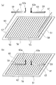
- FIGS. 7A, 7B, and 8 show a configuration example of a solar cell string constituting a conventional solar cell module.
- 7A and 7B are explanatory diagrams showing two scenes of the manufacturing process
- FIG. 8 is an explanatory diagram showing a process of laminating and sealing the solar cell string.
- a configuration example of the solar cell string shown in FIGS. 7 and 8 is also described in Patent Document 1.
- the solar battery cell 115 is formed by laminating a transparent electrode film made of a transparent conductive film, a photoelectric conversion layer, and a back electrode film on the translucent insulating substrate 111 in this order, although not shown.
- the solar battery 115 configured in this way has a long and narrow strip shape, and has a length extending over almost the entire width of the translucent insulating substrate 111, and adjacent solar battery cells 115. 115, one transparent electrode film and the other back electrode film are connected to each other to form a solar cell string 116 in which a plurality of solar cells 115 are connected in series.
- a linear P-type electrode terminal portion 117 having substantially the same length as the solar cell 115 is formed, and the other end A linear N-type electrode terminal portion 118 having substantially the same length as that of the solar battery cell 115 is formed on the end portion of the back electrode film of the solar battery cell 115.
- These P-type electrode terminal portion 117 and N-type electrode terminal portion 118 serve as an electrode extraction portion.
- An insulating sheet 119 is laid on the solar cell string 116 so as to extend between the central portion of the P-type electrode terminal portion 117 and the central portion of the N-type electrode terminal portion 118.
- the insulating sheet 119 is laid so as not to overlap the P-type electrode terminal portion 117 and the N-type electrode terminal portion 118.
- a film having good compatibility with the sealing material is preferable, and among them, a PET film, a fluororesin film, and the like are optimal.
- an adhesive resin sheet may be laid between the insulating sheet 119 and the solar battery cell 115 or between the insulating sheet 119 and the lead wire 112 or 113. Alternatively, it may be bonded in advance with an adhesive or the like.
- a positive electrode current collector 120 called a bus bar made of copper foil having the same shape and size as the P-type electrode terminal portion 117 is electrically and mechanically joined to the entire surface of the P-type electrode terminal portion 117.
- a negative electrode current collector 121 having the same shape and size as the N-type electrode terminal portion 118 is electrically and mechanically joined to the entire surface of the N-type electrode terminal portion 118.
- soldering or conductive paste can be used.
- a positive electrode lead wire 122 and a negative electrode lead wire 123 made of a flat cable are arranged in a straight line (or in a parallel state shifted in the width direction) with their tip portions facing each other. ing.
- One end of the positive electrode lead wire 122 is connected to the center position of the positive electrode current collector 120. Further, the other end portion of the positive electrode lead wire 122 is located at a substantially central portion of the solar cell string 116 and is bent so as to rise from the surface of the solar cell string 116 (for example, in a direction perpendicular to the surface). It is an output lead part 122a. Similarly, one end of the negative electrode lead wire 123 is connected to the center position of the negative electrode current collector 121. Further, the other end portion of the negative electrode lead wire 123 is positioned substantially at the center of the solar cell string 116 and is bent so as to rise from the surface of the solar cell string 116 (for example, in a direction perpendicular to the surface). It is an output lead part 123a.
- the insulating sheet 119 is interposed between the solar cells 115. There is no short circuit.
- the width of the insulating sheet 119 is preferably sufficiently larger than the width of the positive electrode lead wire 122 and the negative electrode lead wire 123, and is arranged in the form of a single sheet from the positive electrode current collector 120 to the negative electrode current collector 121. Yes.
- the sealing film 124 and the weather resistance / resistance of the positive lead wire 122 and the negative lead wire 123 are inserted into the through hole 124 a and the through hole 125 a.
- a back film 125 as a back surface protective material for high insulation is laminated and sealed on the entire surface of the solar cell string 116.
- a thermoplastic polymer film is preferable, and those made of EVA (ethylene vinyl acetate resin) or PVB (polyvinyl butyral resin) are most suitable.
- PET polyethylene terephthalate
- PVF polyvinyl fluoride resin film
- a terminal box (not shown) is provided on each of the output lead portions 122a and 123a of the positive lead wire 122 and the negative lead wire 123 protruding upward from the through hole 125a of the back film 125. Is attached and electrically connected.
- the insulating sheet 119 is laid on the solar cell string 116, and the insulating sheet 119 is formed on the insulating sheet 119. It was necessary to arrange the positive electrode lead wire 122 and the negative electrode lead wire 123 made of a flat cable. In this case, it is necessary to make the width of the insulating sheet 119 sufficiently wider than the widths of the positive electrode lead wire 122 and the negative electrode lead wire 123 in consideration of the positional deviation at the time of laying, and from the positive electrode current collector 120 to the negative electrode Since the current collector 121 is disposed in the form of a single belt-like sheet, it is necessary to use a large amount of insulating sheets. For this reason, there is a problem in that the member cost increases, and it is necessary to pay sufficient attention to the laying of the insulating sheet and the arrangement of the positive electrode lead wire 122 and the negative electrode lead wire 123, and the manufacturing efficiency is also lowered.
- the positive electrode lead wire 122 and the negative electrode lead wire 123 are entirely covered with an insulating film having high heat resistance. That is, the positive electrode lead wire 122 is entirely covered with an insulating film except for one end connected to the positive electrode current collector 120 and the other end connected to the terminal block of the terminal box. The whole is covered with an insulating film except for one end connected to the negative electrode current collector 121 and the other end connected to the terminal block of the terminal box.
- the positive electrode lead wire 122 and the negative electrode lead wire 123 are disposed on the solar cell string 116, the positive electrode lead wire 122 and the negative electrode lead are not laid without laying the insulating sheet 119. It becomes possible to arrange the wire 123 directly on the solar cell string 116, reduce the member cost by omitting the insulating sheet 119, reduce the number of man-hours, and ease of arrangement (that is, worry about short-circuiting even if there is some deviation). This makes it possible to improve manufacturing efficiency.
- Patent Document 1 when the root portion of the output lead portions 122a and 123a is bent in order to stand up vertically, for example, since the stiffness and bounce due to the covering insulating film becomes strong, it is intended to be bent vertically. However, there was a problem of falling down diagonally. Therefore, when the sealing insulating film 124 and the back film 125 are laminated and sealed on the entire surface of the solar cell string 116, the output lead portions 122a and 123a, the through holes 124a of the sealing insulating film 124, and the through holes 125a of the back film 125. There is a problem that the alignment process is difficult and the laminating process takes time.
- the present invention was devised to solve such problems, and its purpose is to allow the positive electrode lead wire and the negative electrode lead wire to be directly disposed on the solar cell string, thereby omitting the insulating sheet.
- a solar cell module that facilitates alignment between an output lead portion, a sealing insulating film, and a back film through-hole when a sealing insulating film and a back film are laminated and sealed over the entire surface of a solar cell string.
- the solar cell module of the present invention is configured by connecting in series a solar cell in which a transparent electrode film, a photoelectric conversion layer, and a back electrode film are stacked in this order on a translucent insulating substrate.
- a solar cell string is formed, and a covered lead wire is disposed on the back electrode film in a state where one end is connected to an electrode extraction portion provided at an end portion of the solar cell string.
- the lead wire on the tip portion side including the bent portion is insulated on one side. It is characterized by being a coating. More specifically, the single-sided insulation coating is provided on the back electrode film side of the lead wire.
- the lead wire has a single-sided insulation coating that penetrates through the through hole of the back film laminated on the solar battery cell, and from that part to the terminal block of the terminal box placed on the back film The contact portion is not covered with insulation.
- the lead wire when the lead wire is arranged on the solar cell string and the output lead portion is bent at a predetermined angle (for example, in the vertical direction) to bend the root portion, this portion has one side of the lead wire.
- the insulating film only on the insulating film, the stiffness and rebound caused by the insulating film are weakened, and the output lead portion can be easily bent at a predetermined angle. Therefore, when the back film is laminated and sealed on the entire surface of the solar cell string, the alignment of the output lead portion and the through hole of the back film becomes easy, and the time for the laminating process can be shortened.
- the lead wire has a single-sided insulation coating in the portion that penetrates the through hole of the back film, and is not insulated from the portion to the portion that contacts the terminal block of the terminal box placed on the back film.
- an insulation film may be caught between the terminal block and the lead wire, resulting in poor soldering. Absent.
- the lead wire 122 is attached to the terminal block 302 of the terminal box 301 as shown in FIG.
- the covering portion 131a may enter between the lead wire 122 or 123 and the terminal block 302, and a soldering failure may occur.
- the single-sided insulation coating can be formed by sticking an insulating tape on one side of the lead wire, or by removing one side of the coated lead wire covering both sides.
- the solar cell module of the present invention is a solar cell string in which solar cells formed by laminating a transparent electrode film, a photoelectric conversion layer, and a back electrode film in this order on a translucent insulating substrate are connected in series.
- the lead wire is disposed on the back electrode film with one end connected to the electrode lead-out portion provided at the end of the solar cell string, and the other end of the lead wire is connected to the back electrode.
- the surface of the lead wire on the back electrode film side is covered on one side with an insulating film.
- the insulating film only on one side of the lead wire, the usage amount of the insulating film can be suppressed to the minimum necessary, and the component cost can be reduced. Moreover, since this insulating film is provided on the back electrode film side of the solar cell string, it is possible to easily arrange and position the lead wire on the solar cell string.
- the lead wire has a single-sided insulation coating up to the portion that penetrates the through hole of the back film, and is not insulated from the portion to the portion that contacts the terminal block of the terminal box placed on the back film. . Therefore, when soldering the lead wire to the terminal block, even if there is a deviation in the position or length of the lead wire, an insulation film may be sandwiched between the terminal block and the lead wire, resulting in poor soldering. Absent.
- the said single-sided insulation coating can be formed by sticking an insulating tape on the single side
- the output lead portion when the root portion of the output lead portion is bent to rise to a predetermined angle, an insulating film is provided only on one side of the lead wire at this portion, thereby reducing stiffness and bounce due to the insulating film.
- the output lead portion can be easily bent at a predetermined angle. Therefore, when the back film is laminated and sealed on the entire surface of the solar cell string, the alignment of the output lead portion and the through hole of the back film becomes easy, and the time of the laminating process can be shortened. Further, by providing the insulating film only on one side of the lead wire, the amount of the insulating film used can be minimized, and the component cost can be reduced. Moreover, since this insulating film is provided on the back electrode film side of the solar cell string, it is possible to easily arrange and position the lead wire on the solar cell string.
- FIG. 1 shows a configuration example of a solar cell string according to Embodiment 1 of the present invention, and (a) and (b) show two scenes of the manufacturing process.
- FIG. 2 is an explanatory diagram illustrating a process of laminating and sealing the solar cell string according to the first embodiment of the present invention.
- FIG. 3 is a partially enlarged perspective view of the periphery of the output lead portion according to the first embodiment of the present invention.
- FIG. 4 is a partially enlarged perspective view of the periphery of the output lead portion according to the second embodiment of the present invention.
- FIG. 5 shows an embodiment of a terminal box according to the present invention, where (a) is a sectional view and (b) is a plan view.
- FIG. 1 shows a configuration example of a solar cell string according to Embodiment 1 of the present invention, and (a) and (b) show two scenes of the manufacturing process.
- FIG. 2 is an explanatory diagram illustrating a process of laminating and sealing the solar cell
- FIG. 6 is a perspective view of the terminal box shown in FIG.
- FIG. 7 shows a configuration example of a conventional solar cell string, and (a) and (b) show two scenes of the manufacturing process.
- FIG. 8 is an explanatory view showing a process of laminating and sealing a conventional solar cell string.
- FIG. 9 is a partial enlarged cross-sectional view showing a state in which the lead wire of the conventional solar cell string is soldered to the terminal block.
- FIGS. 1A and 1B are explanatory diagrams showing two scenes of the manufacturing process
- FIG. 2 is an explanatory diagram showing a process of laminating and sealing the solar cell string.
- the solar battery cell 55 is formed by laminating a transparent electrode film made of a transparent conductive film, a photoelectric conversion layer, and a back electrode film in this order on the translucent insulating substrate 51, although not shown.
- a transparent electrode film made of a transparent conductive film, a photoelectric conversion layer, and a back electrode film in this order on the translucent insulating substrate 51, although not shown.
- the light-transmitting insulating substrate there are heat-resistant resins such as glass and polyimide.
- the transparent electrode film include SnO 2 , ZnO, and ITO.
- the photoelectric conversion layer include silicon-based photoelectric conversion films such as amorphous silicon and microcrystalline silicon, and compound-based photoelectric conversion films such as CdTe and CuInSe 2 .
- the solar cell 55 configured in this way is a long and narrow strip, has a length that covers almost the entire width of the translucent insulating substrate 51, and is adjacent to the solar cell 55. 55, one transparent electrode film and the other back electrode film are connected to each other, so that a solar cell string 56 in which a plurality of solar cells 55 are connected in series is configured.
- a linear P-type electrode terminal portion 57 having substantially the same length as that of the solar battery cell 55 is formed on the end of the transparent electrode film of the solar battery cell 55 at one end of the solar battery string 56, and the other end.
- a linear N-type electrode terminal portion 58 having substantially the same length as that of the solar battery cell 55 is formed on the end portion of the back electrode film of the solar battery cell 55.
- the P-type electrode terminal portion 57 and the N-type electrode terminal portion 58 serve as an electrode extraction portion.
- a positive electrode current collector 60 called a bus bar made of a copper foil having the same shape and size as the P-type electrode terminal 57 is electrically and mechanically joined to the entire surface of the P-type electrode terminal 57.
- a negative electrode current collector 61 having substantially the same shape and size as the type electrode terminal part 58 is electrically and mechanically joined to the entire surface of the N type electrode terminal part 58. As these joining means, soldering or conductive paste can be used.
- the positive electrode lead wire 62 and the negative electrode lead wire 63 made of a flat cable covered with an insulating film (hereinafter referred to as “insulating film”) 59 are in a straight line with the tip portions thereof facing each other. (Or in a parallel state shifted in the width direction).
- One end portion of the positive electrode lead wire 62 is connected to the central position of the positive electrode current collector 60, and the other end portion is positioned at the substantially central portion of the solar cell string 56, with respect to the surface of the solar cell string 56.
- the output lead portion 62a is bent at a predetermined angle (vertical direction in the first embodiment).
- one end portion of the negative electrode lead wire 63 is connected to the central position of the negative electrode current collector 61, and the other end portion is positioned at a substantially central portion of the solar cell string 56, with respect to the surface of the solar cell string 56.
- the output lead portion 63a is bent at a predetermined angle (vertical direction in the first embodiment).
- the bending angle (predetermined angle) of the output lead portions 62a and 63a is not necessarily limited to the vertical direction because it is related to the shape of the terminal box, but is vertical in the first embodiment and the second embodiment. It will be described below as being bent.
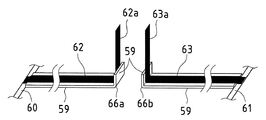
- FIG. 3 is a partially enlarged perspective view showing the periphery of the output lead portions 62a and 63a.
- the output lead portions 62a and 63a are in a state where the lead wire on the tip end side including the bent portions 66a and 66b is covered with the insulating film 59 on one side. More specifically, the insulating film 59 in this portion is provided on the back electrode film side of the solar cell string 56 of the lead wires 62 and 63. That is, when the root portions of the output lead portions 62a and 63a are bent in order to rise vertically, the insulating film 59 is provided only on one side of each of the lead wires 62 and 63 at this portion. Due to the weakness and bounce due to, it can be easily bent vertically.
- the positive electrode lead wire 62 and the negative electrode lead wire 63 are made of the same material (that is, copper foil) as the positive electrode current collector portion 60 and the negative electrode current collector portion 61. As a joining means between each lead wire and the current collector portion, Soldering or spot welding can be used. Although the positive electrode lead wire 62 and the negative electrode lead wire 63 extend over the plurality of solar cells 55, the lead wires 62 and 63 are entirely covered with the insulating film 59, so that the plurality of solar cells. 55 is not short-circuited.
- the sealing insulating film 64 and the weather resistance in a state where the output lead portions 62a and 63a of the positive electrode lead wire 62 and the negative electrode lead wire 63 are inserted into the through hole 64a and the through hole 65a.
- a back film 65 as a back surface protective material for high insulation is laminated and sealed on the entire surface of the solar cell string 56.
- the sealing insulating film 64 may be PVB, silicone, or the like as long as it has good adhesion to the back film 65, the insulating film 59, and the solar battery cell 55 and is excellent in long-term weather resistance.
- Acetate resin is the most suitable for solar cells.
- the back film 65 preferably has a three-layer structure including a moisture-proof layer (in this case, an Al layer) such as PET / Al / PET (PET: polyethylene terephthalate).
- a moisture-proof layer in this case, an Al layer
- PET polyethylene terephthalate
- the back film 65 is set to 100 ⁇ m with respect to the insulating film 59: 50 ⁇ m and the sealing insulating film 124: 600 ⁇ m.
- a terminal box which will be described later, is provided on each of the output lead portions 62a and 63a of the positive electrode lead wire 62 and the negative electrode lead wire 63 protruding upward from the through hole 65a of the back film 65. 10 is attached and electrically connected.
- each lead wire 62, 63 is covered on the back film 65 from the portion of the back film 65 where the portion penetrating the through hole 65a is covered with the insulating film 59. Since the portion of the terminal box 10 that contacts the terminal block 20 is not covered with insulation, when the output lead portions 62a and 63a are soldered to the terminal block 20, the positions and lengths of the output lead portions 62a and 63a are determined. Even when the displacement occurs, the insulating film 59 is not sandwiched between the terminal block 20 and the output lead portions 62a and 63a, and soldering failure does not occur.
- the electrode arrangement structure of the solar cell string 56 is merely an example, and is not limited to such an arrangement structure.
- the arrangement position of the positive electrode lead wire 62 and the negative electrode lead wire 63 may be closer to one end side than the central portion of the solar cell string 56, and it is not necessary to draw out to the central portion. That is, the output lead portions 62a and 63a may be disposed so as to protrude upward from the vicinity of the positive electrode current collector 60 and the negative electrode current collector 61.
- each of the lead wires 62 and 63 is entirely covered with the insulating film 59 from the current collecting portions 60 and 61 to the front of the bent portions 66a and 66b, and the tip including the bent portions 66a and 66b.
- the output lead portions 62a and 63a on the side of the portion are coated on one side with the insulating film 59.
- the entire surface including the bent portion 66 up to the tip end side is a single-sided coating with the insulating film 59. More specifically, the insulating film 59 is provided on the back electrode film side of the solar cell string 56 of each lead wire 62 and 63.
- the insulating film 59 is provided only on one side of each of the lead wires 62 and 63 at this portion. Due to the weakness and bounce due to, it can be easily bent vertically. Further, by providing the insulating film 59 on only one side over almost the entire length of each of the lead wires 62 and 63 in this way, the usage amount of the insulating film can be suppressed to the necessary minimum, leading to a reduction in component costs. Can do.
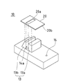
- FIG. 5 shows one configuration example of the terminal box according to the present embodiment, in which (a) is a schematic sectional view and (b) is a plan view.
- FIG. 5 is a perspective view showing the terminal block portion in a separated state.
- the terminal box is attached to each of the rising terminal portion 62a of the positive electrode current collector 20 and the rising terminal portion 63a of the negative electrode current collector 21, the mounting structure is the same. Then, the case where it attaches to the rising terminal part 62a of the positive electrode current collection part 20 is demonstrated.
- the terminal box 10 of the present embodiment is placed and fixed on the back film 65 of the solar cell string 56 in order to electrically connect the output lead portion 62a drawn from the back surface (back film 65) of the solar cell string 56.
- the box case 11 includes a case main body 12 that is placed and fixed on the back film 65 of the solar cell string 56, and a terminal block fixing portion 13 for mounting and fixing the terminal block 20 on the case main body 12. It is made up of.
- the box case 11 is formed in a rectangular parallelepiped shape that is long in the left-right direction and short in the width direction in the figure, and the terminal block fixing portion 13 is formed as a whole. It is formed in a substantially cubic shape.
- the opening 14 (14 a, 14 b, 20 a) for passing the output lead portion 62 a up to the upper side of the terminal block 20 is formed from the bottom surface of the case body 11 to the terminal block 20. It is formed in a series up to the top surface.
- the opening part 14a formed in the terminal block fixing part 13 is a pair of terminals erected at a predetermined interval in the left-right direction of the case body 11, as shown in FIG.
- the terminal fixing pieces 13a and 13b are formed, and the terminal block fixing pieces 13a and 13b form an opening 14a through which the output lead 62a passes. That is, the opening 14a formed in the terminal block fixing portion 13 is not a so-called hole having a cylindrical shape, but has a structure like a groove having both left and right sides opened.
- the potting material is It is easy to flow from the opening 14 a into the opening 14 b of the case body 11 (and further to the back film 65 of the solar cell string 56), and the periphery of the output lead 62 a drawn out from the solar cell string 56 is surely resinated. It becomes possible to seal.
- the opening 20a of the terminal block 20 has a rectangular shape that is long in the width direction.
- the opening part 14b formed in the case main body 11 is formed in the square shape seeing from the plane, and each inner wall surface communicates with the terminal block fixing part 13 (that is, the opening part 14a).
- the terminal block fixing part 13 that is, the opening part 14a.
- the taper By forming the taper in this way, the diameter of the lower end portion of the opening 14b through which the output lead portion 62a is inserted becomes large. Therefore, when the terminal box 10 is covered from above, the output lead portion 62a is connected to the opening 14b. It is possible to prevent problems such as bending when hitting the edge.
- the terminal block 20 is formed in a quadrangular shape in accordance with the shape of the upper surface of the terminal block fixing portion 13, but one edge portion 20b bends the distal end portion 62a1 of the output lead portion 62a. It protrudes from the terminal block fixing part 13 so that it can be stopped.
- the output lead 62a protruding upward from the opening 20a of the terminal block 20 is pressed against the edge of the opening 20a as it is (as shown in FIG. 1).
- the tip end 62a1 of the output lead 62a is locked to the terminal block 20 by bending the bent lead end against the one edge 20b of the terminal block 20 and bending it downward. It can be fixed.
- the tip of the output lead portion 62a can be obtained only by performing two folding steps with the two edges of the edge 20b of the terminal block 20 and the one edge 20b of the terminal block 20 as the starting points. 62a1 can be securely locked and fixed to the terminal block 20. This makes it possible to stably perform the next step of soldering the bent portion of the output lead portion 62a to the terminal block 20, and to provide a terminal box mounting structure that fully complies with the IEC standard.
- the output lead 62a protruding upward from the opening 20a of the terminal block 20 is bent as it is against the edge of the opening 20a and bent to the right side of the terminal block 20, and the bent tip is further exposed.
- the terminal 20 is pressed against the right edge 20b of the terminal block 20 and is bent until it is folded downward.
- the output lead 62a protruding upward from the opening 20a of the terminal block 20 is opened as it is.
- the terminal block 20 is bent to the left side so as to be pressed against the edge of the terminal 20a, and the bent tip is pressed against the left side edge 20c of the terminal block 20 so as to be bent downward until it is folded back. Good.
- the surface side of the output lead 62a that is not covered with the insulating film 59 contacts the terminal block 20, so that when the lead wire 62 is soldered to the terminal block 20, the output lead portion of the lead 62 Even when the position or length of 62a is deviated, the insulating film 59 is not sandwiched between the terminal block 20 and the output lead portion 62a, so that a soldering failure does not occur.
- an air vent hole 16 extending from the bottom surface to the top surface may be provided at an appropriate position of the case body 11.
- the air hole 16 is provided at a position sufficiently away from the terminal block fixing portion 13.
- the bottom surface of the case body 12 of the terminal box 10 has a periphery (even around the entire circumference, for example, four corners). Good) is coated with a silicon resin 18 for adhesion. Therefore, when the terminal box 10 is bonded and fixed onto the back film 65 of the solar cell string 56, a gap S is formed between the bottom surface of the case body 12 and the back film 65 of the solar cell string 56 by the thickness of the silicon resin 18. It will be possible.
- the air vent hole 16 when the potting material flows into the opening 14, it exists in the gap S between the inside of the opening 14 and the back film 65 of the solar cell string 56 and the bottom surface of the case body 12 of the terminal box 10. Since the air that has escaped from the air vent hole 16 to the outside, the potting material is removed from the opening 14 (more specifically, to the back film 65 of the solar cell string 56 in the opening 14, and further to the solar cell string 56.
- the back film 65 and the bottom surface of the case body 12 of the terminal box 10 can be reliably filled (to a gap S), and resin sealing without voids can be performed.
- the external output line fixed to the terminal block 20 can be fixed directly by connecting the connecting end of the external output line to the other end of the terminal block 20 using a rivet or the like. It may be caulked.
- the terminal box 10 is attached on the back film 65 of the solar cell string 56, the output lead 62a is electrically connected to the terminal block 20, and the external output line is electrically connected to the terminal block 20. By connecting, a solar cell module is produced.
- the alignment between the output lead portion and the through hole of the back film becomes easy, and the time of the laminating process can be shortened. Further, by providing the insulating film only on one side of the lead wire, the amount of the insulating film used can be minimized, and the component cost can be reduced. Furthermore, since the insulating film is provided on the back electrode film side of the solar cell string, it is possible to easily arrange and position the lead wire on the solar cell string, which is beneficial.
Abstract
太陽電池ストリング(56)の端部に設けられた電極取り出し部(60,61)に一端部が接続された状態で各リード線(62,63)が太陽電池ストリング(56)の裏面電極膜上に配置され、この各リード線(62,63)の他端部を裏面電極膜の面から立ち上げるように折り曲げて出力リード部(62a,62b)が形成されている太陽電池モジュールにおいて、前記出力リード部(62a,62b)は、折り曲げ部(66a,66b)を含む先端部側のリード線の片面のみが絶縁フィルム(59)で被覆されている。
Description
本発明は、太陽電池ストリングの裏面から引き出される出力リード線の引き出し構造に特徴を有する太陽電池モジュールに関する。
建物の屋根等に複数枚の太陽電池ストリングをマトリックス状に敷設して太陽光発電を行う太陽光発電システムが広く一般に普及しはじめている。このような太陽電池発電システムにおいて、各太陽電池モジュールには、隣接して敷設された他の太陽電池モジュールと互いに電気的に接続可能とするための端子ボックスが備えられている。
従来の太陽電池モジュールを構成する太陽電池ストリングの一構成例を図7(a),(b)及び図8に示す。ただし、図7(a),(b)は製造工程の2つの場面を示す説明図、図8は太陽電池ストリングをラミネート封止する工程を示す説明図である。なお、この図7及び図8に示す太陽電池ストリングの構成例は特許文献1にも記載されている。
太陽電池セル115は、透光性絶縁基板111上に、図示は省略しているが透明導電膜からなる透明電極膜、光電変換層、裏面電極膜がこの順に積層されて形成されている。
このように構成された太陽電池セル115は、図7(a)に示すように細長い短冊状で、透光性絶縁基板111のほぼ全幅にわたる長さを有しており、隣接する太陽電池セル115,115同士において一方の透明電極膜と他方の裏面電極膜とが互いに接続されることで複数の太陽電池セル115が直列に接続された太陽電池ストリング116が構成されている。
この太陽電池ストリング116における一端部の太陽電池セル115の透明電極膜の端部上に、太陽電池セル115とほぼ同一長さの線状のP型電極端子部117が形成され、他端部の太陽電池セル115の裏面電極膜の端部上に、太陽電池セル115とほぼ同一長さの線状のN型電極端子部118が形成されている。これらP型電極端子部117及びN型電極端子部118が電極取り出し部になる。
このP型電極端子部117の中央部とN型電極端子部118の中央部との間をわたすようにして、太陽電池ストリング116の上に絶縁シート119が敷設されている。この絶縁シート119は、P型電極端子部117及びN型電極端子部118には重ならないように敷設されている。絶縁シート119としては、封止材と相性の良いフィルムが好ましく、なかでもPETフィルムやフッ素樹脂フィルムなどが最適である。また、絶縁シートの接着性を確保するために、絶縁シート119と太陽電池セル115の間や、絶縁シート119とリード線112もしくは113との間に接着用の樹脂シートを敷設しても良いし、接着剤などであらかじめ接着しておいても良い。
一方、P型電極端子部117と同形・同大の銅箔からなるバスバーと呼ばれる正極集電部120が、P型電極端子部117の全面に対して電気的かつ機械的に接合されている。同様に、N型電極端子部118と同形・同大の負極集電部121が、N型電極端子部118の全面に対して電気的かつ機械的に接合されている。これらの接合手段としては、半田付けまたは導電性ペーストなどを用いることができる。
絶縁シート119の上には、フラットケーブルからなる正極リード線122と負極リード線123とが、互いの先端部を対向させた状態で一直線状に(若しくは幅方向にずらせた平行状態に)配置されている。
正極リード線122の一端部は、正極集電部120の中央位置に接続されている。また、正極リード線122の他端部は、太陽電池ストリング116のほぼ中央部に位置し、かつ太陽電池ストリング116の面から立ち上げるように(例えば、面に対して垂直方向に)折り曲げられて出力リード部122aとなっている。同様に、負極リード線123の一端部は、負極集電部121の中央位置に接続されている。また、負極リード線123の他端部は、太陽電池ストリング116のほぼ中央部に位置し、かつ太陽電池ストリング116の面から立ち上げるように(例えば、面に対して垂直方向に)折り曲げられて出力リード部123aとなっている。
正極リード線122及び負極リード線123は、複数の太陽電池セル115上にまたがっているが、太陽電池セル115との間に絶縁シート119が介在されているので、これら複数の太陽電池セル115をショートすることはない。絶縁シート119の幅は、正極リード線122及び負極リード線123の幅よりも充分に広いことが望ましく、正極集電部120から負極集電部121まで1枚の帯状シートの形で配置されている。
この状態において、図8に示すように、正極リード線122及び負極リード線123の各出力リード部122a,123aを貫通孔124a及び貫通孔125aに挿通する状態で、封止フィルム124と耐候性・高絶縁性のための裏面保護材としてのバックフィルム125とが、太陽電池ストリング116の全面にラミネート封止されている。封止フィルム124としては、熱可塑性の高分子フィルムが好ましく、なかでもEVA(エチレンビニルアセテート樹脂)製やPVB(ポリビニルブチラール樹脂)製のものなどが最適である。また、バックフィルム125としては、防湿性確保のためにPET/Al/PET(PET:ポリエチレンテレフタレート)の3層構造やPVF/Al/PVF(PVF:ポリフッ化ビニル樹脂フィルム)の3層構造などの防湿層を含むものが好ましい。
このように構成された太陽電池ストリング116において、バックフィルム125の貫通孔125aから上方に向けて突出している正極リード線122及び負極リード線123の各出力リード部122a,123aに、図示しない端子ボックスを取り付けて電気的に接続している。
このように、従来の太陽電池モジュールの構成及び製造方法においては、数多くの煩雑な作業が必要であり、特に、太陽電池ストリング116の上に絶縁シート119を敷設し、この絶縁シート119の上にフラットケーブルからなる正極リード線122と負極リード線123とを配置する必要があった。この場合、敷設時の位置ずれを考慮して、絶縁シート119の幅を、正極リード線122及び負極リード線123の幅よりも充分に広くする必要があり、また、正極集電部120から負極集電部121まで1枚の帯状シートの形で配置されているため、大量の絶縁シートを使用する必要があった。そのため、部材コストの上昇を招くとともに、絶縁シートの敷設と正極リード線122及び負極リード線123の配置に十分注意する必要があり、製造効率も低下するといった問題があった。
そこで、このような問題を解決すべく、特許文献1に記載の太陽電池モジュールでは、正極リード線122及び負極リード線123を耐熱性の高い絶縁フィルムで全体を被覆している。すなわち、正極リード線122は、正極集電部120に接続する一端部と、端子ボックスの端子台に接続する他端部とを除いて全体が絶縁フィルムで被覆されており、負極リード線123は、負極集電部121に接続する一端部と、端子ボックスの端子台に接続する他端部とを除いて全体が絶縁フィルムで被覆されている。このように絶縁フィルムで全体を被覆することで、太陽電池ストリング116の上に正極リード線122及び負極リード線123を配置するとき、絶縁シート119を敷設することなく、正極リード線122及び負極リード線123を太陽電池ストリング116の上に直接配置することが可能となり、絶縁シート119を省略することによる部材コストの低減や、工数の削減、配置の容易性(すなわち、多少ずれてもショートする心配がないため)による製造効率の向上などが可能となるものである。
しかし、特許文献1のものでは、出力リード部122a,123aを例えば垂直に立ち上げるためにその根元部分を折り曲げるとき、被覆している絶縁フィルムによるコシや跳ね返りが強くなるため、垂直に折り曲げたつもりでも、斜めに倒れてしまうといった問題があった。そのため、封止絶縁フィルム124とバックフィルム125とを太陽電池ストリング116の全面にラミネート封止するとき、出力リード部122a,123aと封止絶縁フィルム124の貫通孔124a及びバックフィルム125の貫通孔125aとの位置合わせが難しく、ラミネート工程に時間がかかるといった問題があった。
本発明はかかる問題点を解決すべく創案されたもので、その目的は、正極リード線及び負極リード線を太陽電池ストリングの上に直接配置可能とすることで、絶縁シートを省略することによる部材コストの低減、工数の削減、配置の容易性を確保するとともに、出力リード部を所定角度に立ち上げるためにその根元部分を折り曲げるとき、被覆している絶縁フィルムによるコシや跳ね返りを弱くすることで、封止絶縁フィルムとバックフィルムとを太陽電池ストリングの全面にラミネート封止するときの出力リード部と封止絶縁フィルム及びバックフィルムの貫通孔との位置合わせを容易とした太陽電池モジュールを提供することにある。
上記課題を解決するため、本発明の太陽電池モジュールは、透光性絶縁基板に、透明電極膜、光電変換層、裏面電極膜がこの順に積層されて形成されている太陽電池セルを直列に接続して太陽電池ストリングが形成され、この太陽電池ストリングの端部に設けられた電極取り出し部に一端部が接続された状態で被覆リード線が前記裏面電極膜上に配置され、この被覆リード線の他端部を前記裏面電極膜の面から立ち上げるように折り曲げて出力リード部が形成されている太陽電池モジュールにおいて、前記出力リード部は、前記折り曲げ部を含む先端部側のリード線が片面絶縁被覆であることを特徴としている。より具体的には、前記片面絶縁被覆は、前記リード線の前記裏面電極膜側に設けられている。
また、前記リード線は、前記太陽電池セル上に積層されたバックフィルムの貫通孔に貫通する部分が片面絶縁被覆であり、その部分から前記バックフィルム上に載置された端子ボックスの端子台に接触する部分までは絶縁被覆されていない構成としている。
このように、本発明では、リード線を太陽電池ストリング上に配置し、出力リード部を所定角度(例えば垂直方向)に立ち上げるためにその根元部分を折り曲げるとき、この部分にはリード線の片面のみに絶縁膜を設けることで、絶縁膜によるコシや跳ね返りを弱くし、これによって、出力リード部を容易に所定角度に折り曲げることが可能となる。そのため、バックフィルムを太陽電池ストリングの全面にラミネート封止するとき、出力リード部とバックフィルムの貫通孔との位置合わせが容易となり、ラミネート工程の時間を短縮することが可能となる。また、リード線は、バックフィルムの貫通孔に貫通する部分が片面絶縁被覆であり、その部分からバックフィルム上に載置された端子ボックスの端子台に接触する部分までは絶縁被覆されていないので、リード線の端子台への半田付けのとき、リード線の位置や長さにずれが生じた場合でも、端子台とリード線との間に絶縁フィルムが挟まって半田付け不良が発生することもない。因みに、上記特許文献1のように、正極リード線122及び負極リード線123を絶縁フィルム131で全体を被覆している場合、図9に示すように、端子ボックス301の端子台302にリード線122または123を半田付けするとき、被覆部分131aがリード線122または123と端子台302との間に入り込んで、半田付け不良が発生する可能性がある。
なお、前記片面絶縁被覆は、リード線の片面に絶縁テープを貼着することにより、または両面を被覆した被覆リード線の片側を除去することにより形成することができる。
また、本発明の太陽電池モジュールは、透光性絶縁基板に、透明電極膜、光電変換層、裏面電極膜がこの順に積層されて形成されている太陽電池セルを直列に接続して太陽電池ストリングが形成され、この太陽電池ストリングの端部に設けられた電極取り出し部に一端部が接続された状態でリード線が前記裏面電極膜上に配置され、このリード線の他端部を前記裏面電極膜の面から立ち上げるように折り曲げて出力リード部が形成されている太陽電池モジュールにおいて、前記リード線の前記裏面電極膜側の面が絶縁膜で片面被覆されていることを特徴としている。
このように、リード線の片面のみに絶縁膜を設けることで、絶縁膜の使用量を必要最小限に抑えることができ、部品コストの低減につなげることができる。また、この絶縁フィルムは、太陽電池ストリングの裏面電極膜側に設けられているので、太陽電池ストリング上へのリード線の配置及び位置決めを容易に行うことができる。
また、リード線は、バックフィルムの貫通孔に貫通する部分までが片面絶縁被覆であり、その部分からバックフィルム上に載置された端子ボックスの端子台に接触する部分までは絶縁被覆されていない。従って、リード線の端子台への半田付けのとき、リード線の位置や長さにずれが生じた場合でも、端子台とリード線の間に絶縁フィルムが挟まって半田付け不良が発生することもない。なお、前記片面絶縁被覆は、リード線の片面に絶縁テープを貼着することにより形成することができる。
本発明によれば、出力リード部を所定角度に立ち上げるためにその根元部分を折り曲げるとき、この部分にはリード線の片面のみに絶縁膜を設けることで、絶縁膜によるコシや跳ね返りを弱くし、これによって出力リード部を所定角度に容易に折り曲げることができる。そのため、バックフィルムを太陽電池ストリングの全面にラミネート封止するとき、出力リード部とバックフィルムの貫通孔との位置合わせが容易となり、ラミネート工程の時間を短縮することができる。また、リード線の片面のみに絶縁膜を設けることで、絶縁膜の使用量を必要最小限に抑えることができ、部品コストの低減につなげることができる。また、この絶縁フィルムは、太陽電池ストリングの裏面電極膜側に設けられているので、太陽電池ストリング上へのリード線の配置及び位置決めを容易に行うことができる。
以下、本発明の実施の形態について、図面を参照して説明する。
<実施例1に係る太陽電池ストリングの説明>
図1(a),(b)及び図2は、本実施例1に係る太陽電池モジュールを示している。ただし、図1(a),(b)は製造工程の2つの場面を示す説明図、図2は太陽電池ストリングをラミネート封止する工程を示す説明図である。
図1(a),(b)及び図2は、本実施例1に係る太陽電池モジュールを示している。ただし、図1(a),(b)は製造工程の2つの場面を示す説明図、図2は太陽電池ストリングをラミネート封止する工程を示す説明図である。
太陽電池セル55は、透光性絶縁基板51上に、図示は省略しているが透明導電膜からなる透明電極膜、光電変換層、裏面電極膜がこの順に積層されて形成されている。透光性絶縁基板としてはガラスやポリイミドなどの耐熱性樹脂がある。透明電極膜としてはSnO2、ZnO、ITOなどがある。光電変換層としてはアモルファスシリコンや微結晶シリコンなどのシリコン系光電変換膜や、CdTe,CuInSe2などの化合物系光電変換膜がある。
このように構成された太陽電池セル55は、図1(a)に示すように細長い短冊状で、透光性絶縁基板51のほぼ全幅にわたる長さを有しており、隣接する太陽電池セル55,55同士において一方の透明電極膜と他方の裏面電極膜とが互いに接続されることで複数の太陽電池セル55が直列に接続された太陽電池ストリング56が構成されている。
そして、この太陽電池ストリング56における一端部の太陽電池セル55の透明電極膜の端部上に、太陽電池セル55とほぼ同一長さの線状のP型電極端子部57が形成され、他端部の太陽電池セル55の裏面電極膜の端部上に、太陽電池セル55とほぼ同一長さの線状のN型電極端子部58が形成されている。これらP型電極端子部57及びN型電極端子部58が電極取り出し部になる。このように太陽電池セル55の長さと電極端子部57,58の長さを全て同一長とすることにより、太陽電池ストリング56の複数の太陽電池セル55を直列に流れてきた電流が局部的に集中することがなく、その電流を均一に取り出すことができるのでシリーズ抵抗ロスの発生を抑制することができる。
そして、P型電極端子部57とほぼ同形・同大の銅箔からなるバスバーと呼ばれる正極集電部60が、P型電極端子部57の全面に対して電気的かつ機械的に接合され、N型電極端子部58とほぼ同形・同大の負極集電部61が、N型電極端子部58の全面に対して電気的かつ機械的に接合されている。これらの接合手段としては、半田付けまたは導電性ペーストなどを用いることができる。
上記構成において、絶縁膜(以下、「絶縁フィルム」という。)59で被覆されたフラットケーブルからなる正極リード線62と負極リード線63とが、互いの先端部を対向させた状態で一直線状に(若しくは幅方向にずらせた平行状態に)配置されている。
そして、正極リード線62の一端部が、正極集電部60の中央位置に接続され、他端部は、太陽電池ストリング56のほぼ中央部に位置し、かつ太陽電池ストリング56の面に対して所定角度(本実施例1では、垂直方向)に折り曲げられて出力リード部62aとなっている。同様に、負極リード線63の一端部が、負極集電部61の中央位置に接続され、他端部は、太陽電池ストリング56のほぼ中央部に位置し、かつ太陽電池ストリング56の面に対して所定角度(本実施例1では、垂直方向)に折り曲げられて出力リード部63aとなっている。なお、出力リード部62a,63aの折り曲げ角度(所定角度)は、端子ボックスの形状と関連するため、必ずしも垂直方向に限定されるものではないが、本実施例1及び次の実施例2では垂直に折り曲げるものとして以下説明する。
図3は、出力リード部62a,63aの周辺部を一部拡大して示す斜視図である。
本実施例1では、出力リード部62a,63aは、折り曲げ部66a,66bを含む先端部側のリード線が絶縁フィルム59による片面被覆の状態となっている。より具体的には、この部分の絶縁フィルム59は、リード線62,63の太陽電池ストリング56の裏面電極膜側に設けられている。すなわち、出力リード部62a,63aを垂直に立ち上げるためにその根元部分を折り曲げるとき、この部分には各リード線62,63の片面のみにしか絶縁フィルム59が設けられていないので、絶縁フィルム59によるコシや跳ね返りが弱いため、容易に垂直に折り曲げることができる。
正極リード線62及び負極リード線63は、正極集電部60及び負極集電部61と同一材料(すなわち、銅箔)で作られており、各リード線と集電部との接合手段としては半田付けまたはスポット溶接などを用いることができる。正極リード線62及び負極リード線63は、複数の太陽電池セル55上にまたがっているが、各リード線62,63は絶縁フィルム59でその全体が被覆されているので、これら複数の太陽電池セル55をショートすることはない。
この状態において、図2に示すように、正極リード線62及び負極リード線63の各出力リード部62a,63aを貫通孔64a及び貫通孔65aに挿通する状態で、封止絶縁フィルム64と耐候性・高絶縁性のための裏面保護材としてのバックフィルム65とが、太陽電池ストリング56の全面にラミネート封止されている。封止絶縁フィルム64としては、PVB、シリコーンなど、バックフィルム65や絶縁フィルム59、太陽電池セル55との接着性が良く長期耐候性に優れたものであればよいが、なかでもEVA(エチレンビニルアセテート樹脂)製のものが太陽電池用としての実績があり最適である。特に封止絶縁フィルム64と絶縁フィルム59とを互いに接着性のよいものを選べば、太陽電池ストリングの防水性を向上することができる。また、バックフィルム65としては、PET/Al/PET(PET:ポリエチレンテレフタレート)などの防湿層(この場合はAl層)を含む3層構造のものが好ましい。厚みの一例を挙げると、絶縁フィルム59:50μm、封止絶縁フィルム124:600μmに対して、バックフィルム65を100μmとする。
このように構成された太陽電池ストリング56において、バックフィルム65の貫通孔65aから上方に向けて突出している正極リード線62及び負極リード線63の各出力リード部62a,63aに、後述する端子ボックス10を取り付けて電気的に接続している。
また、本実施例1では、各リード線62,63は、バックフィルム65の貫通孔65aに貫通する部分が絶縁フィルム59で片面被覆されているが、その部分からバックフィルム65上に載置された端子ボックス10の端子台20に接触する部分までは絶縁被覆されていないので、出力リード部62a,63aの端子台20への半田付けのとき、出力リード部62a,63aの位置や長さにずれが生じた場合でも、端子台20と出力リード部62a,63aとの間に絶縁フィルム59が挟まって半田付け不良が発生することもない。
なお、太陽電池ストリング56の電極配置構造はあくまで一例であり、このような配置構造に限定されるものではない。例えば、正極リード線62及び負極リード線63の配置位置は、太陽電池ストリング56の中央部ではなく、一方の端部側に寄っていてもよく、また、中央部まで引き出す必要もない。すなわち、正極集電部60及び負極集電部61の近傍から各出力リード部62a,63aが上方に突出するように配置されていてもよい。
<実施例2に係る太陽電池ストリングの説明>
上記実施例1では、各リード線62,63は、各集電部60,61から折り曲げ部66a,66bの手前までが絶縁フィルム59による全面被覆となっており、折り曲げ部66a,66bを含む先端部側の出力リード部62a,63aが絶縁フィルム59による片面被覆となっているが、本実施例2では、図4に示すように、各集電部60,61から出力リード部62a,63aの折り曲げ部66を含む先端部側までの全てが絶縁フィルム59による片面被覆となっている。より具体的には、この絶縁フィルム59は、各リード線62,63の太陽電池ストリング56の裏面電極膜側に設けられている。すなわち、出力リード部62a,63aを垂直に立ち上げるためにその根元部分を折り曲げるとき、この部分には各リード線62,63の片面のみにしか絶縁フィルム59が設けられていないので、絶縁フィルム59によるコシや跳ね返りが弱いため、容易に垂直に折り曲げることができる。また、このように各リード線62,63のほぼ全長に渡って絶縁フィルム59を片面のみに設けることにより、絶縁フィルムの使用量を必要最小限に抑えることができ、部品コストの低減につなげることができる。
上記実施例1では、各リード線62,63は、各集電部60,61から折り曲げ部66a,66bの手前までが絶縁フィルム59による全面被覆となっており、折り曲げ部66a,66bを含む先端部側の出力リード部62a,63aが絶縁フィルム59による片面被覆となっているが、本実施例2では、図4に示すように、各集電部60,61から出力リード部62a,63aの折り曲げ部66を含む先端部側までの全てが絶縁フィルム59による片面被覆となっている。より具体的には、この絶縁フィルム59は、各リード線62,63の太陽電池ストリング56の裏面電極膜側に設けられている。すなわち、出力リード部62a,63aを垂直に立ち上げるためにその根元部分を折り曲げるとき、この部分には各リード線62,63の片面のみにしか絶縁フィルム59が設けられていないので、絶縁フィルム59によるコシや跳ね返りが弱いため、容易に垂直に折り曲げることができる。また、このように各リード線62,63のほぼ全長に渡って絶縁フィルム59を片面のみに設けることにより、絶縁フィルムの使用量を必要最小限に抑えることができ、部品コストの低減につなげることができる。
<端子ボックスの説明>
図5は、本実施形態に係る端子ボックスの一構成例を示しており、(a)は概略断面図、(b)は平面図である。また、図5は、端子台部分を分離した状態で示した斜視図である。ただし、端子ボックスは、正極集電部20の立ち上がり端子部62a、及び負極集電部21の立ち上がり端子部63aのそれぞれに取り付けられるものであるが、その取り付け構造は同じであるので、本実施形態では、正極集電部20の立ち上がり端子部62aに取り付けた場合について説明する。
図5は、本実施形態に係る端子ボックスの一構成例を示しており、(a)は概略断面図、(b)は平面図である。また、図5は、端子台部分を分離した状態で示した斜視図である。ただし、端子ボックスは、正極集電部20の立ち上がり端子部62a、及び負極集電部21の立ち上がり端子部63aのそれぞれに取り付けられるものであるが、その取り付け構造は同じであるので、本実施形態では、正極集電部20の立ち上がり端子部62aに取り付けた場合について説明する。
本実施形態の端子ボックス10は、太陽電池ストリング56の裏面(バックフィルム65)から引き出された出力リード部62aを電気的に接続するために、太陽電池ストリング56のバックフィルム65上に載置固定されるボックスケース11と、このボックスケース11上に形成された端子台20とからなっている。また、ボックスケース11は、太陽電池ストリング56のバックフィルム65上に載置固定されるケース本体12と、このケース本体12の上部に前記端子台20を載置固定するための端子台固定部13とからなっている。
本実施形態では、ボックスケース11は、図5(b)に示すように、この図中の左右方向に長く、幅方向に短い直方体形状に形成されており、端子台固定部13は、全体として略立方体形状に形成されている。
このようなボックスケース11の構成において、本実施形態では、出力リード部62aを端子台20の上方まで通すための開口部14(14a,14b,20a)が、ケース本体11の底面から端子台20の上面まで一連に形成されている。
ここで、本実施形態では、端子台固定部13に形成される開口部14aは、図6に示すように、ケース本体11の左右方向に所定の間隔を存して立設された一対の端子台固定片13a,13bによって形成され、この端子台固定片13a,13bの間が、出力リード部62aを通すための開口部14aとなっている。すなわち、端子台固定部13に形成される開口部14aは、円筒形のようないわゆる穴ではなく、左右両側が開放された溝のような構造となっている。そのため、この端子ボックス10に出力リード部62a及び図示しない外部出力線(隣接配置される他の太陽電池モジュールと接続するための線)を接続した後、ポッティングによって樹脂封止するとき、ポッティング材が開口部14aからケース本体11の開口部14b内部に(さらには、太陽電池ストリング56のバックフィルム65まで)流入し易くなり、太陽電池ストリング56から引き出された出力リード部62aの周辺を確実に樹脂封止することが可能となる。
なお、このような開口部14aの形状に合わせて、端子台20の開口部20aも、幅方向に長い長方形状となっている。
また、本実施形態では、ケース本体11に形成された開口部14bは、平面からみて四角形状に形成されており、各内壁面は、端子台固定部13に連通する側(すなわち、開口部14aの下端縁)からケース本体11の底面に向かって漸次拡開するテーパ状に形成されている。このようにテーパ状に形成することで、出力リード部62aを挿通する開口部14bの下端部の口径が大きくなることから、端子ボックス10を上から被せるとき、出力リード部62aが開口部14bの縁部に当たって折れ曲がってしまうといった不具合を防止することができる。
また、本実施形態では、端子台20は、端子台固定部13の上面形状に合わせて四角形状に形成されているが、一方の縁部20bが、出力リード部62aの先端部62a1を折り曲げ係止可能なように、端子台固定部13から突出して設けられている。すなわち、本実施形態では、端子台20の開口部20aから上方に突出した出力リード部62aをそのまま開口部20aの縁部に押し当てるようにして端子台20の一方の縁部側(図1では右側)に折り曲げ、その折り曲げ先端部をさら端子台20の一方の縁部20bに押し当てるようにして、下方に折り返すまで折り曲げることにより、出力リード部62aの先端部62a1を端子台20に係止固定することが可能となる。すなわち、端子台20の開口部20aの縁部、及び端子台20の一方の縁部20bの2点をそれぞれ折り曲げ起点として、2回の折り曲げ工程を実施するだけで、出力リード部62aの先端部62a1を端子台20に確実に係止固定することが可能となる。これにより、出力リード部62aの折り曲げ部分を端子台20に半田付けする次の工程を安定して行うことが可能となり、IEC規格に十分準拠した端子ボックスの取り付け構造とすることができる。
なお、図5では、端子台20の開口部20aから上方に突出した出力リード部62aをそのまま開口部20aの縁部に押し当てるようにして端子台20の右側に折り曲げ、その折り曲げ先端部をさら端子台20の右側縁部20bに押し当てるようにして、下方に折り返すまで折り曲げているが、これとは逆に、端子台20の開口部20aから上方に突出した出力リード部62aをそのまま開口部20aの縁部に押し当てるようにして端子台20の左側に折り曲げ、その折り曲げ先端部をさら端子台20の左側縁部20cに押し当てるようにして、下方に折り返すまで折り曲げるように構成してもよい。この方向に折り曲げる場合、出力リード部62aの絶縁フィルム59で被覆されていない面側が端子台20に接触するので、リード線62の端子台20への半田付けのとき、リード線62の出力リード部62aの位置や長さにずれが生じた場合でも、端子台20と出力リード部62aとの間に絶縁フィルム59が挟まって半田付け不良が発生することがない。
また、本実施形態では、ケース本体11の適所に、底面から上面まで達する空気抜き孔16を設けた構成としてもよい。ただし、この空気孔16は、端子台固定部13から十分離れた位置に設けるものとする。端子ボックス10を太陽電池ストリング56のバックフィルム65に取り付けるため、端子ボックス10のケース本体12の底面には、その周囲(全周であっても、例えば隅角部の4箇所等であってもよい)に接着用のシリコン樹脂18が塗布されている。従って、端子ボックス10を太陽電池ストリング56のバックフィルム65上に接着固定すると、このシリコン樹脂18の厚み分だけ、ケース本体12の底面と太陽電池ストリング56のバックフィルム65との間に隙間Sができることになる。従って、空気抜き孔16を設けることで、ポッティング材が開口部14に流れ込むとき、開口部14内部及び太陽電池ストリング56のバックフィルム65と端子ボックス10のケース本体12の底面との隙間Sに存在している空気が、空気抜き孔16から外部に抜けるため、ポッティング材を開口部14内(より具体的には、開口部14内の太陽電池ストリング56のバックフィルム65まで、さらには太陽電池ストリング56のバックフィルム65と端子ボックス10のケース本体12の底面との隙間Sまで)確実に充填することができ、空隙の無い樹脂封止を行うことが可能となる。
なお、図示は省略しているが、この端子台20に固定される外部出力線の固定方法としては、外部出力線の接続端部を端子台20の他方の端部にリベット等を用いて直接かしめるようにしてもよい。このように、太陽電池ストリング56のバックフィルム65上に端子ボックス10を取り付けて、端子台20に出力リード部62aを電気的に接続し、さらに、この端子台20に外部出力線を電気的に接続することで、太陽電池モジュールが作製される。
本発明は、その精神または主要な特徴から逸脱することなく、他のいろいろな形で実施することができる。そのため、上述の実施例はあらゆる点で単なる例示にすぎず、限定的に解釈してはならない。本発明の範囲は請求の範囲によって示すものであって、明細書本文には、なんら拘束されない。さらに、請求の範囲の均等範囲に属する変形や変更は、全て本発明の範囲内のものである。
なお、この出願は、日本で2008年6月4日に出願された特願2008-147025号に基づく優先権を請求する。その内容はこれに言及することにより、本出願に組み込まれるものである。また、本明細書に引用された文献は、これに言及することにより、その全部が具体的に組み込まれるものである。
本発明によれば、バックフィルムを太陽電池ストリングの全面にラミネート封止するときに、出力リード部とバックフィルムの貫通孔との位置合わせが容易となり、ラミネート工程の時間を短縮することができる。また、リード線の片面のみに絶縁膜を設けることで、絶縁膜の使用量を必要最小限に抑えることができ、部品コストの低減につなげることができる。さらに、この絶縁フィルムは、太陽電池ストリングの裏面電極膜側に設けられているので、太陽電池ストリング上へのリード線の配置及び位置決めを容易に行うことが可能であり、有益である。
10 端子ボックス
11 ボックスケース
12 ケース本体
13 端子台固定部
13a,13b 端子台固定片
14(14a,14b,20a) 開口部
16 空気抜き孔
20 端子台
20b 右側の縁部
20c 左側の縁部
51 透光性絶縁基板
55 太陽電池セル
56 太陽電池ストリング(薄膜太陽電池ストリング)
57 P型電極端子部
58 N型電極端子部
59 絶縁膜(絶縁フィルム)
60 正極集電部
61 負極集電部
62 正極リード線
63 負極リード線
62a,63a 立ち上がり端子部
62a1 先端部
64 封止絶縁フィルム
65 バックフィルム
64a,65a 貫通孔
11 ボックスケース
12 ケース本体
13 端子台固定部
13a,13b 端子台固定片
14(14a,14b,20a) 開口部
16 空気抜き孔
20 端子台
20b 右側の縁部
20c 左側の縁部
51 透光性絶縁基板
55 太陽電池セル
56 太陽電池ストリング(薄膜太陽電池ストリング)
57 P型電極端子部
58 N型電極端子部
59 絶縁膜(絶縁フィルム)
60 正極集電部
61 負極集電部
62 正極リード線
63 負極リード線
62a,63a 立ち上がり端子部
62a1 先端部
64 封止絶縁フィルム
65 バックフィルム
64a,65a 貫通孔
Claims (7)
- 透光性絶縁基板に、透明電極膜、光電変換層、裏面電極膜がこの順に積層されて形成されている太陽電池セルを直列に接続して太陽電池ストリングが形成され、この太陽電池ストリングの端部に設けられた電極取り出し部に一端部が接続された状態で被覆リード線が前記裏面電極膜上に配置され、この被覆リード線の他端部を前記裏面電極膜の面から立ち上げるように折り曲げて出力リード部が形成されている太陽電池モジュールにおいて、
前記出力リード部は、前記折り曲げ部を含む先端部側のリード線が片面絶縁被覆であることを特徴とする太陽電池モジュール。 - 請求項1に記載の太陽電池モジュールにおいて、
前記片面絶縁被覆は、前記リード線の前記裏面電極膜側に設けられていることを特徴とする太陽電池モジュール。 - 請求項2に記載の太陽電池モジュールにおいて、
前記リード線は、前記太陽電池セル上に積層されたバックフィルムの貫通孔に貫通する部分が片面絶縁被覆であり、その部分から前記バックフィルム上に載置された端子ボックスの端子台に接触する部分までは絶縁被覆されていないことを特徴とする太陽電池モジュール。 - 請求項1から請求項3までのいずれか1項に記載の太陽電池モジュールにおいて、
前記片面絶縁被覆は、リード線の片面に絶縁テープを貼着することにより、または両面を被覆した被覆リード線の片側を除去することにより形成されていることを特徴とする太陽電池モジュール。 - 透光性絶縁基板に、透明電極膜、光電変換層、裏面電極膜がこの順に積層されて形成されている太陽電池セルを直列に接続して太陽電池ストリングが形成され、この太陽電池ストリングの端部に設けられた電極取り出し部に一端部が接続された状態でリード線が前記裏面電極膜上に配置され、このリード線の他端部を前記裏面電極膜の面から立ち上げるように折り曲げて出力リード部が形成されている太陽電池モジュールにおいて、
前記リード線の前記裏面電極膜側の面が絶縁膜で片面被覆されていることを特徴とする太陽電池モジュール。 - 請求項5に記載の太陽電池モジュールにおいて、
前記リード線は、前記太陽電池セル上に積層されたバックフィルムの貫通孔に貫通する部分が片面絶縁被覆であり、その部分から前記バックフィルム上に載置された端子ボックスの端子台に接触する部分までは絶縁被覆されていないことを特徴とする太陽電池モジュール。 - 請求項5または請求項6に記載の太陽電池モジュールにおいて、
前記片面絶縁被覆は、リード線の片面に絶縁テープを貼着することにより形成されていることを特徴とする太陽電池モジュール。
Priority Applications (3)
| Application Number | Priority Date | Filing Date | Title |
|---|---|---|---|
| EP09758346.2A EP2296189A4 (en) | 2008-06-04 | 2009-06-03 | SOLAR CELL MODULE |
| US12/996,428 US20110088749A1 (en) | 2008-06-04 | 2009-06-03 | Solar cell module |
| CN2009801199611A CN102047441B (zh) | 2008-06-04 | 2009-06-03 | 太阳能电池模块 |
Applications Claiming Priority (2)
| Application Number | Priority Date | Filing Date | Title |
|---|---|---|---|
| JP2008-147025 | 2008-06-04 | ||
| JP2008147025A JP4558070B2 (ja) | 2008-06-04 | 2008-06-04 | 太陽電池モジュール |
Publications (1)
| Publication Number | Publication Date |
|---|---|
| WO2009148079A1 true WO2009148079A1 (ja) | 2009-12-10 |
Family
ID=41398152
Family Applications (1)
| Application Number | Title | Priority Date | Filing Date |
|---|---|---|---|
| PCT/JP2009/060149 WO2009148079A1 (ja) | 2008-06-04 | 2009-06-03 | 太陽電池モジュール |
Country Status (5)
| Country | Link |
|---|---|
| US (1) | US20110088749A1 (ja) |
| EP (1) | EP2296189A4 (ja) |
| JP (1) | JP4558070B2 (ja) |
| CN (1) | CN102047441B (ja) |
| WO (1) | WO2009148079A1 (ja) |
Cited By (1)
| Publication number | Priority date | Publication date | Assignee | Title |
|---|---|---|---|---|
| US20120048334A1 (en) * | 2010-08-30 | 2012-03-01 | Cohen Brian E | Photovoltaic module cover |
Families Citing this family (14)
| Publication number | Priority date | Publication date | Assignee | Title |
|---|---|---|---|---|
| AT12058U1 (de) * | 2010-04-27 | 2011-09-15 | Austria Tech & System Tech | Verfahren zum kontaktieren eines photovoltaischen moduls mit einem anschlussgehäuse sowie system bestehend aus einem photovoltaischen modul und einem anschlussgehäuse |
| US8601753B2 (en) * | 2011-01-27 | 2013-12-10 | Certainteed Corporation | Electrical wiring systems for use in roofing applications |
| GB2490499A (en) * | 2011-05-03 | 2012-11-07 | Solaredge Technologies Ltd | Junction box assembly for electrical connections to photovoltaic panels |
| CN102779895A (zh) * | 2011-05-13 | 2012-11-14 | 江伦 | 太阳能电池及其制造方法、光电光热真空管及其接收器 |
| JP6021138B2 (ja) | 2011-05-27 | 2016-11-09 | デクセリアルズ株式会社 | 太陽電池モジュール、太陽電池モジュールの製造方法、及び薄膜太陽電池用タブ線 |
| WO2012167761A1 (de) * | 2011-06-10 | 2012-12-13 | Roesener Thomas | Solarmodul, solarmodulbaugruppe und verfahren zum herstellen eines solarmoduls mit einem mittels umformen hergestellten elektrischen kontaktübergang |
| JP5745349B2 (ja) | 2011-06-27 | 2015-07-08 | デクセリアルズ株式会社 | 太陽電池モジュールの製造方法 |
| JP2013021177A (ja) * | 2011-07-12 | 2013-01-31 | Sharp Corp | 太陽電池モジュール、および太陽電池モジュールの製造方法 |
| WO2013031199A1 (ja) * | 2011-08-30 | 2013-03-07 | 三洋電機株式会社 | 太陽電池モジュール |
| KR101305624B1 (ko) * | 2011-11-01 | 2013-09-09 | 엘지이노텍 주식회사 | 태양전지 모듈 및 이의 제조방법 |
| WO2013073608A1 (ja) * | 2011-11-18 | 2013-05-23 | シャープ株式会社 | 太陽電池モジュール、太陽電池モジュールの製造方法、および太陽電池モジュール製造装置 |
| CN102544377A (zh) * | 2012-02-24 | 2012-07-04 | 日月光半导体制造股份有限公司 | 具有光电池的半导体结构及其制造方法 |
| JP5958701B2 (ja) | 2012-07-17 | 2016-08-02 | デクセリアルズ株式会社 | 配線材、太陽電池モジュール及び太陽電池モジュールの製造方法 |
| US20190267938A1 (en) * | 2018-02-26 | 2019-08-29 | Tesla, Inc. | System and method for coupling junction box to solar roof tiles |
Citations (5)
| Publication number | Priority date | Publication date | Assignee | Title |
|---|---|---|---|---|
| JPH09326497A (ja) | 1996-06-03 | 1997-12-16 | Kanegafuchi Chem Ind Co Ltd | 太陽電池モジュール及びその製造方法 |
| JP2000068542A (ja) * | 1998-08-26 | 2000-03-03 | Sharp Corp | 集積型薄膜太陽電池モジュール |
| JP2001077383A (ja) * | 1999-09-01 | 2001-03-23 | Kanegafuchi Chem Ind Co Ltd | 薄膜太陽電池モジュール及びその製造方法 |
| JP2004140100A (ja) * | 2002-10-16 | 2004-05-13 | Mitsubishi Heavy Ind Ltd | 薄膜太陽電池モジュール |
| JP2008147025A (ja) | 2006-12-11 | 2008-06-26 | Rohm Co Ltd | 半導体集積回路および電子機器 |
Family Cites Families (3)
| Publication number | Priority date | Publication date | Assignee | Title |
|---|---|---|---|---|
| JP3352252B2 (ja) * | 1994-11-04 | 2002-12-03 | キヤノン株式会社 | 太陽電池素子群並びに太陽電池モジュール及びその製造方法 |
| EP1081770B1 (en) * | 1999-09-01 | 2009-02-18 | Kaneka Corporation | Thin-film solar cell module and method of manufacturing the same |
| FR2903714A1 (fr) * | 2006-07-12 | 2008-01-18 | Uriel Moch | Panneau feuillete, procede de fabrication d'un tel panneau et paroi comprenant ce panneau. |
-
2008
- 2008-06-04 JP JP2008147025A patent/JP4558070B2/ja not_active Expired - Fee Related
-
2009
- 2009-06-03 WO PCT/JP2009/060149 patent/WO2009148079A1/ja active Application Filing
- 2009-06-03 EP EP09758346.2A patent/EP2296189A4/en not_active Withdrawn
- 2009-06-03 US US12/996,428 patent/US20110088749A1/en not_active Abandoned
- 2009-06-03 CN CN2009801199611A patent/CN102047441B/zh not_active Expired - Fee Related
Patent Citations (5)
| Publication number | Priority date | Publication date | Assignee | Title |
|---|---|---|---|---|
| JPH09326497A (ja) | 1996-06-03 | 1997-12-16 | Kanegafuchi Chem Ind Co Ltd | 太陽電池モジュール及びその製造方法 |
| JP2000068542A (ja) * | 1998-08-26 | 2000-03-03 | Sharp Corp | 集積型薄膜太陽電池モジュール |
| JP2001077383A (ja) * | 1999-09-01 | 2001-03-23 | Kanegafuchi Chem Ind Co Ltd | 薄膜太陽電池モジュール及びその製造方法 |
| JP2004140100A (ja) * | 2002-10-16 | 2004-05-13 | Mitsubishi Heavy Ind Ltd | 薄膜太陽電池モジュール |
| JP2008147025A (ja) | 2006-12-11 | 2008-06-26 | Rohm Co Ltd | 半導体集積回路および電子機器 |
Non-Patent Citations (1)
| Title |
|---|
| See also references of EP2296189A4 |
Cited By (1)
| Publication number | Priority date | Publication date | Assignee | Title |
|---|---|---|---|---|
| US20120048334A1 (en) * | 2010-08-30 | 2012-03-01 | Cohen Brian E | Photovoltaic module cover |
Also Published As
| Publication number | Publication date |
|---|---|
| JP2009295744A (ja) | 2009-12-17 |
| EP2296189A1 (en) | 2011-03-16 |
| JP4558070B2 (ja) | 2010-10-06 |
| US20110088749A1 (en) | 2011-04-21 |
| CN102047441B (zh) | 2013-03-27 |
| CN102047441A (zh) | 2011-05-04 |
| EP2296189A4 (en) | 2014-05-21 |
Similar Documents
| Publication | Publication Date | Title |
|---|---|---|
| JP4558070B2 (ja) | 太陽電池モジュール | |
| JP4384241B1 (ja) | 端子ボックス及び太陽電池モジュール | |
| JP5268596B2 (ja) | 太陽電池モジュール及びその製造方法 | |
| TWI413266B (zh) | 太陽能電池模組 | |
| US8952240B2 (en) | Solar cell module | |
| JP5031698B2 (ja) | 太陽電池モジュール | |
| JP2009043842A (ja) | 太陽電池モジュール | |
| WO2010010821A1 (ja) | 太陽電池モジュール及びその作成方法 | |
| JP5191406B2 (ja) | 太陽電池モジュールの製造方法 | |
| JP2010283231A (ja) | 太陽電池モジュール及びその製造方法 | |
| JP5132646B2 (ja) | 端子ボックス及び太陽電池モジュール | |
| JP5306490B2 (ja) | 端子ボックス及び太陽電池モジュール | |
| CN101847668A (zh) | 太阳能电池模块 | |
| JP2012142637A (ja) | 太陽電池モジュール | |
| JP2012142635A (ja) | 太陽電池モジュール | |
| JP2012142634A (ja) | 太陽電池モジュール及びその製造方法 | |
| JP5339295B2 (ja) | 太陽電池モジュール及びその製造方法 | |
| JP2002141535A (ja) | 太陽電池モジュールの電力リード引き出し方法 | |
| JP2012142633A (ja) | 太陽電池モジュール及びその製造方法 | |
| JP2012142636A (ja) | 太陽電池モジュール及びその製造方法 | |
| JP2013219281A (ja) | 太陽電池モジュールおよび太陽電池モジュールの製造方法 | |
| JP2013030619A (ja) | 薄膜太陽電池とその製造方法 |
Legal Events
| Date | Code | Title | Description |
|---|---|---|---|
| WWE | Wipo information: entry into national phase |
Ref document number: 200980119961.1 Country of ref document: CN |
|
| 121 | Ep: the epo has been informed by wipo that ep was designated in this application |
Ref document number: 09758346 Country of ref document: EP Kind code of ref document: A1 |
|
| WWE | Wipo information: entry into national phase |
Ref document number: 12996428 Country of ref document: US |
|
| NENP | Non-entry into the national phase |
Ref country code: DE |
|
| WWE | Wipo information: entry into national phase |
Ref document number: 2009758346 Country of ref document: EP |