WO2009136606A1 - 半導体装置の製造方法 - Google Patents
半導体装置の製造方法 Download PDFInfo
- Publication number
- WO2009136606A1 WO2009136606A1 PCT/JP2009/058574 JP2009058574W WO2009136606A1 WO 2009136606 A1 WO2009136606 A1 WO 2009136606A1 JP 2009058574 W JP2009058574 W JP 2009058574W WO 2009136606 A1 WO2009136606 A1 WO 2009136606A1
- Authority
- WO
- WIPO (PCT)
- Prior art keywords
- nitrogen
- film
- containing layer
- silicon nitride
- semiconductor device
- Prior art date
- Legal status (The legal status is an assumption and is not a legal conclusion. Google has not performed a legal analysis and makes no representation as to the accuracy of the status listed.)
- Ceased
Links
Images





Classifications
-
- H—ELECTRICITY
- H10—SEMICONDUCTOR DEVICES; ELECTRIC SOLID-STATE DEVICES NOT OTHERWISE PROVIDED FOR
- H10P—GENERIC PROCESSES OR APPARATUS FOR THE MANUFACTURE OR TREATMENT OF DEVICES COVERED BY CLASS H10
- H10P14/00—Formation of materials, e.g. in the shape of layers or pillars
- H10P14/60—Formation of materials, e.g. in the shape of layers or pillars of insulating materials
- H10P14/69—Inorganic materials
- H10P14/692—Inorganic materials composed of oxides, glassy oxides or oxide-based glasses
- H10P14/6921—Inorganic materials composed of oxides, glassy oxides or oxide-based glasses containing silicon
- H10P14/6922—Inorganic materials composed of oxides, glassy oxides or oxide-based glasses containing silicon the material containing Si, O and at least one of H, N, C, F or other non-metal elements, e.g. SiOC, SiOC:H or SiONC
- H10P14/6927—Inorganic materials composed of oxides, glassy oxides or oxide-based glasses containing silicon the material containing Si, O and at least one of H, N, C, F or other non-metal elements, e.g. SiOC, SiOC:H or SiONC the material being a silicon oxynitride, e.g. SiON or SiON:H
-
- H—ELECTRICITY
- H10—SEMICONDUCTOR DEVICES; ELECTRIC SOLID-STATE DEVICES NOT OTHERWISE PROVIDED FOR
- H10B—ELECTRONIC MEMORY DEVICES
- H10B41/00—Electrically erasable-and-programmable ROM [EEPROM] devices comprising floating gates
- H10B41/30—Electrically erasable-and-programmable ROM [EEPROM] devices comprising floating gates characterised by the memory core region
-
- H—ELECTRICITY
- H10—SEMICONDUCTOR DEVICES; ELECTRIC SOLID-STATE DEVICES NOT OTHERWISE PROVIDED FOR
- H10D—INORGANIC ELECTRIC SEMICONDUCTOR DEVICES
- H10D30/00—Field-effect transistors [FET]
- H10D30/01—Manufacture or treatment
- H10D30/021—Manufacture or treatment of FETs having insulated gates [IGFET]
- H10D30/0413—Manufacture or treatment of FETs having insulated gates [IGFET] of FETs having charge-trapping gate insulators, e.g. MNOS transistors
-
- H—ELECTRICITY
- H10—SEMICONDUCTOR DEVICES; ELECTRIC SOLID-STATE DEVICES NOT OTHERWISE PROVIDED FOR
- H10D—INORGANIC ELECTRIC SEMICONDUCTOR DEVICES
- H10D30/00—Field-effect transistors [FET]
- H10D30/60—Insulated-gate field-effect transistors [IGFET]
- H10D30/68—Floating-gate IGFETs
- H10D30/681—Floating-gate IGFETs having only two programming levels
-
- H—ELECTRICITY
- H10—SEMICONDUCTOR DEVICES; ELECTRIC SOLID-STATE DEVICES NOT OTHERWISE PROVIDED FOR
- H10D—INORGANIC ELECTRIC SEMICONDUCTOR DEVICES
- H10D30/00—Field-effect transistors [FET]
- H10D30/60—Insulated-gate field-effect transistors [IGFET]
- H10D30/68—Floating-gate IGFETs
- H10D30/6891—Floating-gate IGFETs characterised by the shapes, relative sizes or dispositions of the floating gate electrode
- H10D30/6894—Floating-gate IGFETs characterised by the shapes, relative sizes or dispositions of the floating gate electrode having one gate at least partly in a trench
-
- H—ELECTRICITY
- H10—SEMICONDUCTOR DEVICES; ELECTRIC SOLID-STATE DEVICES NOT OTHERWISE PROVIDED FOR
- H10D—INORGANIC ELECTRIC SEMICONDUCTOR DEVICES
- H10D64/00—Electrodes of devices having potential barriers
- H10D64/01—Manufacture or treatment
- H10D64/031—Manufacture or treatment of data-storage electrodes
- H10D64/035—Manufacture or treatment of data-storage electrodes comprising conductor-insulator-conductor-insulator-semiconductor structures
-
- H—ELECTRICITY
- H10—SEMICONDUCTOR DEVICES; ELECTRIC SOLID-STATE DEVICES NOT OTHERWISE PROVIDED FOR
- H10P—GENERIC PROCESSES OR APPARATUS FOR THE MANUFACTURE OR TREATMENT OF DEVICES COVERED BY CLASS H10
- H10P14/00—Formation of materials, e.g. in the shape of layers or pillars
- H10P14/60—Formation of materials, e.g. in the shape of layers or pillars of insulating materials
- H10P14/63—Formation of materials, e.g. in the shape of layers or pillars of insulating materials characterised by the formation processes
- H10P14/6302—Non-deposition formation processes
- H10P14/6316—Formation by nitridation, e.g. nitridation of the substrate
-
- H—ELECTRICITY
- H10—SEMICONDUCTOR DEVICES; ELECTRIC SOLID-STATE DEVICES NOT OTHERWISE PROVIDED FOR
- H10P—GENERIC PROCESSES OR APPARATUS FOR THE MANUFACTURE OR TREATMENT OF DEVICES COVERED BY CLASS H10
- H10P14/00—Formation of materials, e.g. in the shape of layers or pillars
- H10P14/60—Formation of materials, e.g. in the shape of layers or pillars of insulating materials
- H10P14/65—Formation of materials, e.g. in the shape of layers or pillars of insulating materials characterised by treatments performed before or after the formation of the materials
- H10P14/6516—Formation of materials, e.g. in the shape of layers or pillars of insulating materials characterised by treatments performed before or after the formation of the materials of treatments performed after formation of the materials
- H10P14/6518—Formation of materials, e.g. in the shape of layers or pillars of insulating materials characterised by treatments performed before or after the formation of the materials of treatments performed after formation of the materials by introduction of substances into an already-existing insulating layer
- H10P14/6524—Formation of materials, e.g. in the shape of layers or pillars of insulating materials characterised by treatments performed before or after the formation of the materials of treatments performed after formation of the materials by introduction of substances into an already-existing insulating layer the substance being nitrogen
- H10P14/6526—Formation of materials, e.g. in the shape of layers or pillars of insulating materials characterised by treatments performed before or after the formation of the materials of treatments performed after formation of the materials by introduction of substances into an already-existing insulating layer the substance being nitrogen introduced into an oxide material, e.g. changing SiO to SiON
-
- H—ELECTRICITY
- H10—SEMICONDUCTOR DEVICES; ELECTRIC SOLID-STATE DEVICES NOT OTHERWISE PROVIDED FOR
- H10P—GENERIC PROCESSES OR APPARATUS FOR THE MANUFACTURE OR TREATMENT OF DEVICES COVERED BY CLASS H10
- H10P50/00—Etching of wafers, substrates or parts of devices
- H10P50/20—Dry etching; Plasma etching; Reactive-ion etching
- H10P50/28—Dry etching; Plasma etching; Reactive-ion etching of insulating materials
- H10P50/282—Dry etching; Plasma etching; Reactive-ion etching of insulating materials of inorganic materials
- H10P50/283—Dry etching; Plasma etching; Reactive-ion etching of insulating materials of inorganic materials by chemical means
-
- H—ELECTRICITY
- H10—SEMICONDUCTOR DEVICES; ELECTRIC SOLID-STATE DEVICES NOT OTHERWISE PROVIDED FOR
- H10W—GENERIC PACKAGES, INTERCONNECTIONS, CONNECTORS OR OTHER CONSTRUCTIONAL DETAILS OF DEVICES COVERED BY CLASS H10
- H10W10/00—Isolation regions in semiconductor bodies between components of integrated devices
- H10W10/01—Manufacture or treatment
- H10W10/011—Manufacture or treatment of isolation regions comprising dielectric materials
- H10W10/014—Manufacture or treatment of isolation regions comprising dielectric materials using trench refilling with dielectric materials, e.g. shallow trench isolations
- H10W10/0145—Manufacture or treatment of isolation regions comprising dielectric materials using trench refilling with dielectric materials, e.g. shallow trench isolations of trenches having shapes other than rectangular or V-shape
-
- H—ELECTRICITY
- H10—SEMICONDUCTOR DEVICES; ELECTRIC SOLID-STATE DEVICES NOT OTHERWISE PROVIDED FOR
- H10W—GENERIC PACKAGES, INTERCONNECTIONS, CONNECTORS OR OTHER CONSTRUCTIONAL DETAILS OF DEVICES COVERED BY CLASS H10
- H10W10/00—Isolation regions in semiconductor bodies between components of integrated devices
- H10W10/10—Isolation regions comprising dielectric materials
- H10W10/17—Isolation regions comprising dielectric materials formed using trench refilling with dielectric materials, e.g. shallow trench isolations
Definitions
- the present invention relates to a method for manufacturing a semiconductor device.
- a typical flash memory includes a floating gate electrode paired with a control gate electrode. Electrons are injected into the floating gate electrode when data is written, and electrons are emitted from the floating date electrode when data is erased. Such a flash memory further includes an insulating film covering the floating gate electrode. Since the insulating film prevents leakage of electrons injected into the floating gate electrode, the flash memory can store data for a long period unless power is supplied from an external circuit.
- the insulating film that covers the floating gate electrode for example, a tunnel insulating film or an interlayer capacitance film having an ONO (Oxide-Nitride-Oxide) structure is made thick, electrons are less likely to leak from the floating gate electrode. Characteristics can be improved. However, if the insulating film covering the floating gate electrode is thickened, the efficiency of electron injection / discharge to the floating gate electrode is lowered, and the data writing and erasing characteristics are lowered.
- ONO Oxide-Nitride-Oxide
- Patent Document 1 When the silicon nitride film is formed by ion implantation of nitrogen into the floating gate electrode as in Patent Document 1, the silicon nitride film is formed by unevenly distributing nitrogen only at the interface between the floating gate electrode and the insulating film. Is possible.
- the technique of Patent Document 1 is disadvantageous in that heat treatment is indispensable after nitrogen implantation, which may increase the thermal budget, and it is difficult to strictly control the distribution of implanted nitrogen. It is.
- plasma nitriding is known as means for forming a silicon nitride film by introducing nitrogen thinly into the surface of the silicon layer, and this can also be applied to nitriding of the floating gate electrode.
- the plasma nitriding treatment is advantageous in that the nitrogen distribution controllability is higher than the method of performing heat treatment after nitrogen ion implantation as in Patent Document 1. Further, since nitriding can be performed at a low temperature of, for example, about 400 ° C. to 600 ° C. by using plasma, various problems due to heat treatment at a high temperature of 800 ° C. or higher as in Patent Document 1 can be avoided.
- a silicon nitride film is formed on the surface of a floating gate electrode of a flash memory
- a plasma nitriding process is performed after forming the floating gate electrode on a silicon substrate, not only the surface of the floating gate electrode but also adjacent cells are formed.
- the surface of the element isolation film to be isolated is also nitrided to form a silicon nitride oxide film.
- an originally unnecessary nitrogen-containing layer (silicon nitride oxide film) remains in the element isolation film of the completed flash memory.
- the unnecessary silicon oxynitride film remaining in this manner may cause electrical interference between adjacent cells, which may reduce the data retention performance of the flash memory.
- the present invention has been made in view of the above circumstances, and an object of the present invention is to provide a method for manufacturing a semiconductor device that does not leave a nitrogen-containing layer formed by plasma nitriding treatment in unnecessary portions in the manufacturing process of various semiconductor devices. is there.
- a field region and an active region are defined by an element isolation film containing oxygen, and an electrode layer and a nitrogen-containing layer formed in contact with the electrode layer are formed in the active region.
- a method for manufacturing a semiconductor device includes a plasma nitriding treatment step in which nitrogen-containing plasma is applied to the exposed electrode layer and the exposed element isolation film to form a nitrogen-containing layer in each of the electrode layer and the element isolation film, and the electrode And a selective etching step in which the nitrogen-containing layer formed on the surface of the element isolation film is selectively removed while leaving the nitrogen-containing layer formed on the surface of the layer.
- the manufacturing method according to the first aspect wherein the electrode layer includes polysilicon as a main component, and the nitrogen-containing layer formed on the electrode layer is silicon nitride. provide.
- a third aspect of the present invention is the manufacturing method according to the first or second aspect, wherein the element isolation film contains silicon oxide as a main component, and the nitrogen-containing layer formed on the element isolation film is nitrided and oxidized
- a manufacturing method is provided that is silicon.
- a manufacturing method according to any one of the first to third aspects, wherein a wet etching process using a diluted hydrofluoric acid solution is performed in the selective etching step. .
- a fifth aspect of the present invention is the manufacturing method according to any one of the first to fourth aspects, wherein the nitrogen concentration in the nitrogen-containing layer formed on the electrode layer in the plasma nitriding treatment step is 35 atom% or more.
- a production method in the range of 45 atom% or less is provided.
- the electrode layer is a floating gate electrode of a nonvolatile memory
- the silicon nitride film is a part of an interlayer capacitance film interposed between the floating gate electrode and the control gate electrode. It is preferable that it comprises.
- a sixth aspect of the present invention is the manufacturing method according to any one of the first to fifth aspects, wherein the electrode layer is a floating gate electrode of a nonvolatile memory, and the silicon nitride film is connected to the floating gate electrode.
- the electrode layer is a floating gate electrode of a nonvolatile memory
- the silicon nitride film is connected to the floating gate electrode.
- a manufacturing method which is a part of an interlayer capacitance film interposed between control gate electrodes.
- the selective etching process is performed, the unnecessary nitrogen-containing layer formed on the surface of the element isolation film can be selectively removed while leaving the nitrogen-containing layer formed on the surface.
- an adverse influence caused by an unnecessary nitrogen-containing layer for example, electrical interference between adjacent cells can be prevented, and reliability can be improved.
- FIG. 7 is a cross-sectional view showing a structure of a flash memory manufactured by a method of manufacturing a semiconductor device according to a second embodiment of the present invention.
- FIG. It is drawing explaining the process of the manufacturing method of the semiconductor device by the 2nd Embodiment of this invention. It is drawing explaining the process following FIG. It is drawing explaining the process following FIG. It is drawing explaining the process following FIG. It is drawing explaining the process following FIG. It is sectional drawing which shows the structure of the flash memory of a comparative example. It is drawing explaining the mechanism of the electronic leakage in the flash memory of a comparative example.
- 1 is a barrier height diagram of a flash memory manufactured by a method of manufacturing a semiconductor device according to an embodiment of the present invention.
- FIG. 1A to 1C are diagrams for explaining a part of a manufacturing process of a semiconductor device according to the present embodiment.
- a recess (trench) is formed in the silicon substrate 101 by, for example, an STI (Shallow Trench Isolation) method, and an element isolation film 103 substantially made of silicon dioxide (SiO 2 ) is formed in the recess.
- STI Shallow Trench Isolation
- An insulating film 105 made of silicon dioxide (SiO 2 ) is formed on the surface of the silicon substrate 101, and an electrode layer 107 made of substantially polysilicon is formed thereon.
- a nitrogen-containing plasma is applied to the silicon substrate 101 from which the electrode layer 107 and the element isolation film 103 are exposed, whereby the electrode layer 107 and the element isolation film 103 are formed.
- a plasma nitriding process for forming a nitrogen-containing layer on the surface, and a selection for selectively removing the nitrogen-containing layer formed on the surface of the element isolation film 103 while leaving the nitrogen-containing layer formed on the surface of the electrode layer 107 An etching process.
- FIG. 1A shows a silicon substrate 101 whose surface has been subjected to plasma nitriding treatment
- FIG. 1B shows the silicon substrate 101 that has undergone plasma nitriding treatment.
- a silicon nitride (SiN) film 109 as a nitrogen-containing layer is formed on the surface of the electrode layer 107.
- the silicon substrate 101 is exposed to plasma having high ion energy, so that the surfaces of the element isolation film 103 and the insulating film 105 are also nitrided, and a nitrogen-containing layer is formed on the surfaces of the element isolation film 103 and the insulating film 105.
- a silicon nitride oxide film (SiON) 111 is formed.
- unnecessary silicon nitride oxide film 111 formed on the surfaces of element isolation film 103 and insulating film 105 may be removed in a subsequent process, but is not removed.
- the semiconductor device for example, MOSFET
- the semiconductor device may eventually remain.
- silicon nitride oxide (SiON) has more defects such as vacancies than dense silicon dioxide (SiO 2 ), it tends to work as a path through which electrons pass. In other words, there is a concern that the performance of the semiconductor device may be deteriorated because electrons leak to an adjacent cell through an electrical defect present in the remaining silicon nitride oxide film 111.
- a selective etching process is provided after the plasma nitridation process, leaving the silicon nitride film 109 formed on the electrode layer 107, and the isolation film 103 and the insulating film.
- the silicon nitride oxide film 111 formed on the surface of the film 105 is removed.
- the selective etching process as shown in FIG. 1C, the silicon nitride oxide film 111 formed on the surfaces of the element isolation film 103 and the insulating film 105 is removed.
- the selective etching treatment step is preferably performed immediately after the plasma nitridation treatment step or at least before a treatment involving subsequent heating is performed.
- treatment with heating is performed with the silicon nitride oxide film 111 remaining, nitrogen atoms in the silicon nitride oxide film 111 diffuse into the element isolation film 103 and the insulating film 105, and the element isolation film 103 and the insulating film 105 This is because the effective thickness is reduced and its function is reduced.
- the difference in solubility between silicon nitride (SiN) and silicon nitride oxide (SiON) in the etching solution is used.
- wet etching conditions and plasma nitriding conditions are considered.
- dilute hydrofluoric acid which dissolves silicon oxide and hardly dissolves silicon nitride as an etchant.
- concentration of dilute hydrofluoric acid used depends on the thickness of the nitrogen-containing layer, but is preferably in the range of 0.07% or more and 1% or less, more preferably in the range of 0.1% or more and 0.3% or less. preferable.
- the treatment time with dilute hydrofluoric acid depends on the thickness of the nitrogen-containing layer and the concentration of dilute hydrofluoric acid, but the silicon nitride oxide film 111 can be removed and the silicon nitride film 109 can be left as much as possible. For example, in the range of 10 seconds or more, considering the time margin, the range of 30 seconds to 300 seconds is more preferable, and the range of 150 seconds to 210 seconds is more preferable.
- the electron temperature of the generated plasma is 0.7 eV or more and 2 eV or less on the wafer surface, and the thickness (depth) range is several nm (eg, 2 nm or more and 5 nm or less) with a good controllability and is at a certain level. It is preferable to employ a method in which nitrogen can be introduced at the above relatively high concentration (for example, 35 atom% or more, preferably 40 atom% or more).
- a microwave-excited plasma is formed by introducing a microwave into the processing chamber by a planar antenna having a plurality of slots (for example, a radial line slot antenna (RLSA)) in the plasma nitriding process.
- a plasma processing apparatus is used.
- ICP inductively coupled plasma
- a wafer W on which the electrode layer 107 and the element isolation film 103 are formed is prepared, and this wafer W is carried into a plasma processing apparatus.
- an inert gas and a nitrogen-containing gas are respectively introduced into the chamber at a predetermined flow rate from the gas supply mechanism while evacuating the inside of the chamber of the plasma processing apparatus. In this way, the inside of the chamber is adjusted to a predetermined pressure.
- a microwave having a predetermined frequency, for example, 2.45 GHz, generated by the microwave generator is supplied to the planar antenna through the matching circuit and the waveguide.
- the microwaves radiated from the planar antenna through the transmission plate into the chamber excite the plasma of the inert gas and the nitrogen-containing gas in the chamber.
- This microwave-excited plasma has a high density of about 1 ⁇ 10 10 to 5 ⁇ 10 12 / cm 3 and a low electron temperature in the vicinity of the wafer W of about 1.2 eV or less.
- Such microwave-excited high-density plasma has little plasma damage caused by ions or the like on the underlying film.
- a plasma nitridation process is performed on the electrode layer 107 and the element isolation film 103 formed on the surface of the wafer W by active species such as ions or radicals in the plasma.
- the volume flow rate ratio of the N 2 gas to the total processing gas is preferably in the range of 1% or more and 90% or less from the viewpoint of increasing the nitrogen concentration in the silicon nitride oxide film 111 (FIG. 1B) to be formed, A range of 2% to 20% is more preferable.
- the flow rate of Ar gas is in the range of 200 mL / min (sccm) to 2000 mL / min (sccm), and the flow rate of N 2 gas is 10 mL / min (sccm) or more.
- the flow rate ratio can be set within the range of 2000 mL / min (sccm) or less.
- the pressure in the chamber of the plasma processing apparatus during plasma nitriding is preferably in the range of 1.3 Pa or more and 667 Pa or less from the viewpoint of enhancing plasma ionicity and increasing the nitrogen concentration in the nitrogen-containing layer. Within the range of 3 Pa or more and 400 Pa or less is more preferable.
- the power density of the microwave in order to maintain the plasma stably, 1.4 W / cm 2 or more 7W / cm 2 within the range are preferred.
- the microwave power density means the microwave power supplied per 1 cm 2 area of the transmission plate (the same applies hereinafter). For example, when processing a wafer W having a diameter of 200 mm or more, it is preferable that the microwave power is in a range of 1000 W to 5000 W.
- the heating temperature of the wafer W is preferably set within a range of 200 ° C. or more and 600 ° C. or less, for example, as the temperature of the mounting table provided in the chamber and on which the wafer W is mounted. It is more preferable to set the temperature within a range of ° C or less.
- the nitrided wafer W is unloaded from the plasma processing apparatus.
- a silicon dioxide film (SiO 2 ), an amorphous silicon film (a-Si), or a polysilicon film (Poly-Si) is deposited on a silicon substrate, respectively, and samples “SiO 2 ”, “a-Si”, and A sample “Poly-Si” was prepared. The thickness of these films was in the range of 20 nm to 30 nm. A silicon substrate (Bare-Si) on which no film was deposited was also prepared as a sample “Bare-Si”.
- the etching time was 60 seconds, 180 seconds and 300 seconds.
- the nitrogen concentration in the nitrogen-containing layer was measured by XPS (X-ray photoelectron spectroscopy).
- XPS X-ray photoelectron spectroscopy
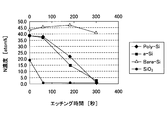
- the etching rates of the sample “Poly-Si”, the sample “a-Si”, and the sample “Bare-Si” in which silicon is nitrided are the etching rates of the sample “SiO 2 ” in which silicon dioxide is nitrided. It can be seen that it is very different from the rate. Focusing on the sample “SiO 2 ”, the nitrogen concentration becomes almost zero in 180 seconds in FIG. 2A and in 60 seconds in FIG. 2B, and the nitrogen-containing layer (silicon nitride oxide film) is removed.
- the nitrogen concentration was hardly lowered in the same etching time, and the nitrogen-containing layer ( The silicon nitride film) remained almost. Thereby, it can be seen that the silicon nitride oxide film was selectively removed.
- FIG. 2A comparing FIG. 2A in which the plasma nitriding treatment was performed under the condition 1 and FIG. 2B in which the plasma nitriding treatment was performed under the condition 2
- a sample “Poly-Si” obtained by nitriding silicon is shown in FIG.
- the nitrogen concentration in “a-Si” and the sample “Bare-Si” does not decrease greatly even when the etching time is long, and it is shown that it is preferable from the viewpoint of selective etching that leaves the silicon nitride film.
- condition 1 the plasma nitridation treatment was performed for 90 seconds even at a relatively low pressure of 20 Pa, so that the nitrogen concentration at the start of etching was as shown in FIG.
- FIG. 3 shows the nitrogen concentration in the film at the time of starting etching and the etching for the samples “Poly-Si” and Sample “a-Si” that were plasma-nitrided under conditions 1 to 6. The relationship with the physical film thickness of the nitrogen-containing layer at the end time (when the nitrogen concentration of the sample “SiO 2 ” becomes substantially zero) is shown. From FIG.
- the nitrogen concentration in the nitrogen-containing layer should be 35 atom% or more (for example, 35 atom% or more and 45 atom% or less, preferably 40 atom% or more and 45 atom% or less).
- the pressure in the plasma nitriding process is set within the range of 13.3 Pa to 400 Pa, for example. It is preferable that the treatment time is set within a range of, for example, 30 seconds to 240 seconds, and the flow rate ratio of nitrogen gas is preferably set within a range of 1% to 20%.
- an ICP plasma processing apparatus can be used instead of the RLSA plasma processing apparatus.
- the frequency of the high frequency power is preferably in the range of 400 kHz to 60 MHz (for example, 13.56 MHz), and the high frequency power is preferably in the range of 50 W to 2000 W.
- the processing temperature (mounting table temperature) is preferably in the range of 100 ° C. to 600 ° C., and the processing pressure is preferably in the range of 0.13 Pa to 667 Pa.
- Ar gas and N 2 gas are preferably used, and the Ar gas flow rate is preferably in the range of 100 mL / min (sccm) to 2000 mL / min (sccm), and the N 2 flow rate is 1 mL / min ( sccm) or more and 500 mL / min (sccm) or less is preferable.
- the frequency of high frequency power is 13.56 MHz
- the high frequency power is 500 W
- the processing temperature is 400 ° C.
- the processing pressure is 6.7 Pa
- the Ar gas flow rate is 1000 mL / min (sccm)
- the N 2 gas flow rate is 50 mL /
- the ICP plasma processing apparatus can also be applied to the semiconductor device manufacturing method of the present embodiment, like the RLSA plasma processing apparatus.
- FIG. 4 is a sectional view showing a schematic configuration of a flash memory that can be manufactured by applying the manufacturing method according to the embodiment of the present invention.
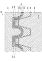
- This flash memory 200 has a laminated structure of NONON (silicon nitride film-silicon oxide film-silicon nitride film-silicon oxide film-silicon nitride film) as an interlayer capacitance film interposed between the floating gate electrode and the control gate electrode. is doing.
- NONON silicon nitride film-silicon oxide film-silicon nitride film-silicon oxide film-silicon nitride film
- a recess is formed in a silicon substrate 201 by, for example, STI (Shallow Trench Isolation) method, and an element isolation film 205 is embedded in the inside through a liner silicon oxide film 203.
- a floating gate electrode 209 made of, for example, polysilicon is formed on the convex portion of the silicon substrate 201 (between two adjacent concave portions) with a tunnel insulating film 207 interposed therebetween.
- the floating gate electrode 209 that is a part for accumulating charges is covered with an interlayer capacitance film 221.
- the interlayer capacitance film 221 includes a first silicon nitride film 211, a first silicon oxide film 213, a second silicon nitride film 215, a second silicon oxide film 217, and a third silicon nitride film, which are sequentially stacked from the inside. 219.
- a control gate electrode 223 made of, for example, polysilicon is formed on the interlayer capacitance film 221, and the flash memory 200 is configured.
- the first silicon nitride film 211 is formed so as to cover the surface of the floating gate electrode 209, but is not formed on the element isolation film 205. With such a structure, the flash memory 200 can suppress interference between adjacent cells, specifically, movement of electrons, and can exhibit excellent data retention characteristics. This point will be described later.
- FIG. 5 shows a cross-sectional structure of the main part of the wafer W to be subjected to plasma nitriding.
- a floating gate electrode 209 mainly composed of polysilicon is formed on the silicon substrate 201 with a tunnel insulating film 207 interposed therebetween.
- the tunnel insulating film 207 and the floating gate electrode 209 can be formed by a known film formation process, a photolithography technique, and an etching process.
- the inner surface of the recess of the silicon substrate 201 is covered with a liner silicon oxide film 203, and the recess covered with the liner silicon oxide film 203 is embedded with an element isolation film 205.
- the element isolation film 205 defines an active region and a field region in the flash memory memory 200.
- the element isolation film 205 is formed by using, for example, dilute hydrofluoric acid after forming a silicon dioxide (SiO 2 ) film by HDP-CVD (High Density Plasma Chemical Vapor Deposition) method or SOG (Spin-On-Glass) method. It is formed by wet etching and etching back.
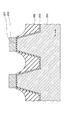
- the nitrogen-containing layer 212 is formed by the plasma nitriding process.
- the nitrogen-containing layer 212 is formed on the surface of the floating gate electrode 209 and the surface of the element isolation film 205.
- a nitrogen-containing layer 212a of silicon nitride (SiN) is formed on the surface of the floating gate electrode 209 mainly composed of polysilicon.
- a nitrogen-containing layer 212b of silicon nitride oxide (SiON) is formed on the surface of the element isolation film 205 made of silicon dioxide (SiO 2 ).
- the plasma nitriding process for forming the nitrogen-containing layer 212 can be performed using the same plasma processing apparatus as in the first embodiment and under the same conditions as in the first embodiment.
- FIG. 7 shows the wafer W (silicon substrate 201) after the selective etching process.
- the selective etching process can be performed under the same conditions as in the first embodiment.
- the nitrogen-containing layer 212b (the portion indicated by the broken line) formed on the surface of the element isolation film 205 is selectively removed, but the nitrogen-containing layer 212a on the surface of the floating gate electrode 209 is almost removed. It remains without.
- This selective etching process utilizes the difference in solubility between silicon nitride (SiN) and silicon nitride oxide (SiON) in an etching solution (dilute hydrofluoric acid).
- the remaining nitrogen-containing layer 212a becomes the first silicon nitride film 211 that is a part of the interlayer capacitance film 221 in the flash memory 200 (see FIG. 4).
- the first silicon oxide film 213, the second silicon nitride film 215, the second silicon oxide film 217, and the third nitride are formed on the first silicon nitride film 211 and the element isolation film 205.
- Silicon films 219 are sequentially stacked to form an interlayer capacitance film 221 as shown in FIG.
- the first silicon oxide film 213 can be formed as an HTO (High-Temperature-Oxide) film by, for example, a low pressure CVD method.
- the second silicon nitride film 215 can be formed by, for example, a low pressure CVD method using DCS (dichlorosilane) as a raw material.
- the second silicon oxide film 217 can be formed as an HTO (High Temperature Oxide) film by, for example, a low pressure CVD method.
- the third silicon nitride film 219 can be formed by, for example, a plasma nitriding method.
- the control gate electrode 223 is formed on the third silicon nitride film 219 by a CVD method, a plasma CVD method or the like, whereby the flash memory 200 having the structure shown in FIG. 4 is manufactured.
- FIG. 9 schematically shows the structure of the flash memory 300 of the comparative example.
- a step of removing the nitrogen-containing layer 212b of silicon nitride oxide (SiON) formed on the surface of the element isolation film 205 is not provided after the plasma nitriding process. Therefore, the flash memory 300 is different from the flash memory 200 shown in FIG. 4 in that the interlayer capacitance film 221a is formed on the entire nitrogen-containing layer 212.
- the remaining unnecessary nitrogen-containing layer 212b (silicon nitride oxide film) functions as an electron transfer path and causes interference between adjacent cells, resulting in a problem that data retention characteristics of the flash memory 300 are deteriorated. That is, when the writing state is different between adjacent cells of the flash memory 300 (that is, 0 or 1), the cell in which the charge is injected into the floating gate electrode 209 is adjacent to the cell in which the charge is not injected into the floating gate electrode 209. Electrons move toward the cell through the nitrogen-containing layer 212 in contact with the element isolation film 205, and data retention characteristics are degraded. For example, in FIG.
- a write state in which electrons are injected into the floating gate electrode 209 of one (left side) cell is shown, and the other (right side).
- the floating gate electrode 209 of this cell is in an erased state (write; 0) in which electrons are not injected. If left in this state for a long time, as indicated by an arrow in FIG. 9, electrons are written from the cell in the written state through the nitrogen-containing layer 212 remaining between the element isolation film 205 and the first silicon oxide film 213.
- the threshold voltage of the cell in the write state (write; 1) changes due to the flow toward the erased cell. That is, data cannot be held for a long time.
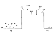
- FIG. 10A schematically shows a band diagram between the floating gate electrode 209 and the control gate electrode 223 in the flash memory 300 of the comparative example.
- the nitrogen-containing layer 212 in contact with the floating gate electrode 209 formed by the plasma nitriding process has a relatively small energy band gap, and thus only provides a relatively low barrier to the floating gate electrode 209. For this reason, electrons leak from the floating gate electrode 209 into the nitrogen-containing layer 212 to a small extent. Then, it is considered that electrons move through the electrical defect in the nitrogen-containing layer 212 to the adjacent cell.
- the nitrogen-containing layer (silicon nitride oxide film; reference numeral 212b in FIG. 6) on the element isolation film 205 is removed by etching.
- the first silicon nitride film 211 terminates around the floating gate electrode 209. Therefore, electrons do not move along the nitrogen-containing layer on the element isolation film 205, and interference between adjacent cells is prevented.
- FIG. 10B in the flash memory 200, a high barrier by the first silicon oxide film 213 directly acts on the floating gate electrode 209, and the first silicon nitride film is formed from the floating gate electrode 209. Electron leakage (tunneling) to 213 is sufficiently reduced.
- an RLSA type or ICP type plasma processing apparatus is used in the step of forming the first silicon nitride film (nitrogen-containing layer).
- a plasma processing apparatus such as electron cyclotron resonance (ECR) plasma, magnetron plasma, surface wave plasma (SWP), or the like may be used. May be used.
- ECR electron cyclotron resonance
- SWP surface wave plasma
- the interlayer capacitance film 221 has a NONON structure.
- the present invention is not limited to this.
- the same applies to the manufacture of a flash memory having a NONO structure from the inside (floating gate electrode side).
- the present invention can be applied to.
Landscapes
- Semiconductor Memories (AREA)
- Formation Of Insulating Films (AREA)
- Non-Volatile Memory (AREA)
- Electrodes Of Semiconductors (AREA)
- Weting (AREA)
Abstract
プラズマ窒化処理工程の後に、選択エッチング処理工程において、電極層に形成された窒化珪素膜を残しつつ、素子分離膜および絶縁膜の表面に形成された窒化酸化珪素膜が除去される。選択エッチング工程により、素子分離膜および絶縁膜の表面に形成された窒化酸化珪素膜が除去される。
Description
本発明は、半導体装置の製造方法に関する。
フラッシュメモリは小さいセルサイズ、大きい記憶容量、および高い衝撃耐性という利点を有しているため、近年、フラッシュメモリに対する需要が急増している。代表的なフラッシュメモリは、コントロールゲート電極と対になるフローティングゲート電極を含んでおり、データ書き込み時にはフローティングゲート電極へ電子が注入され、データ消去時にはフローティングデート電極から電子が放出される。このようなフラッシュメモリはフローティングゲート電極を覆う絶縁膜を更に含んでいる。この絶縁膜によってフローティングゲート電極に注入された電子の漏洩が防止されるため、フラッシュメモリは、外部回路から電力が供給されない限り、長期間にわたってデータを記憶することができる。
フローティングゲート電極を覆う絶縁膜、例えばトンネル絶縁膜やONO(Oxide-Nitride-Oxide)構造を有する層間容量膜などを厚くすれば、フローティングゲート電極から電子が漏洩し難くなるため、フラッシュメモリのデータ保持特性を向上させることができる。しかし、フローティングゲート電極を覆う絶縁膜を厚くすると、フローティングゲート電極への電子の注入/放出の効率が低下するため、データの書込み特性、消去特性が低下してしまう。
また、フラッシュメモリの製造過程では、コントロールゲート電極がエッチングによって形成される際に、多結晶シリコンからなるフローティングゲート電極の側壁が露出してしまうため、熱処理を行って側壁を酸化膜で覆う工程が行われる。しかし、この熱処理によりトンネル絶縁膜やONO構造を有する層間容量膜が酸化されて厚くなってしまうので、フローティングゲート電極への電子の注入/放出の効率が低下するという問題が生じる。この問題を解決するため、フローティングゲート電極を形成した後、フローティングゲート電極に窒素をイオン注入し、800℃以上の温度で熱酸化することにより、フローティングゲート電極表面に酸化珪素膜を形成して、フローティングゲート電極と層間容量膜およびトンネル絶縁膜との界面に窒素を偏在させる(すなわち、窒化珪素膜を形成する)技術が提案されている(特許文献1)。
上記特許文献1のように、フローティングゲート電極に窒素をイオン注入する方法で窒化珪素膜を形成する場合には、フローティングゲート電極と絶縁膜との界面にのみ窒素を偏在させて窒化珪素膜を形成することが可能である。しかし、特許文献1の技術は、窒素注入後に熱処理が不可欠であるため、サーマルバジェットを増大させてしまう懸念があり、また、注入した窒素の分布を厳密に制御することが難しいという点で、不利である。
一方、シリコン層の表面に薄く窒素を導入して窒化珪素膜を形成する手段として、プラズマ窒化処理が知られており、これをフローティングゲート電極の窒化に適用することも可能である。プラズマ窒化処理は、特許文献1のように窒素をイオン注入した後に熱処理する方法に比べて、窒素分布の制御性が高い点で有利である。また、プラズマの使用により、例えば400℃~600℃程度の低温で窒化処理を実施できるため、特許文献1におけるような800℃以上の高温での熱処理による諸問題を回避できる。しかし、プラズマ窒化処理では、選択的な窒化が困難であり、すなわち、被処理体の全露出表面が窒化されてしまうため、窒化が不必要な部分にも窒素含有層が形成されてしまう。このように残存した不必要な窒素含有層が、フラッシュメモリに残存すると、例えば残存した窒素含有層を介して隣接するセル間での電気的な干渉が生じるなど、フラッシュメモリの性能に悪影響を及ぼす場合がある。
例えば、フラッシュメモリのフローティングゲート電極の表面に窒化珪素膜を形成する場合、シリコン基板上にフローティングゲート電極を形成した後にプラズマ窒化処理を行うと、フローティングゲート電極の表面だけでなく、隣接するセルを分離する素子分離膜の表面も窒化されて窒化酸化珪素膜が形成されてしまう。このため、完成品のフラッシュメモリの素子分離膜には、本来不必要な窒素含有層(窒化酸化珪素膜)が残存する。このように残存した不必要な窒化酸化珪素膜は、隣接するセル間で電気的な干渉を引き起こし、フラッシュメモリのデータ保持性能を低下させてしまう場合がある。
本発明は上記実情に鑑みてなされ、その目的は、各種半導体装置の製造過程で、プラズマ窒化処理によって形成された窒素含有層を不必要な部位に残存させない半導体装置の製造方法を提供することである。
本発明の第1の態様は、酸素を含有する素子分離膜によってフィールド領域とアクティブ領域が画定され、前記アクティブ領域に、電極層と、該電極層に接して形成された窒素含有層と、を有する半導体装置の製造方法を提供する。この製造方法は、露出した電極層と露出した素子分離膜とに窒素含有プラズマが作用されて、当該電極層および当該素子分離膜それぞれに窒素含有層が形成されるプラズマ窒化処理工程と、前記電極層の表面に形成された窒素含有層を残しながら前記素子分離膜の表面に形成された窒素含有層が選択的に除去される選択エッチング工程と、を含む。
本発明の第2の態様は、第1の態様の製造方法であって、前記電極層が主成分としてポリシリコンを含み、該電極層に形成された窒素含有層が窒化珪素である製造方法を提供する。
本発明の第3の態様は、第1または第2の態様の製造方法であって、前記素子分離膜が主成分として酸化珪素を含み、該素子分離膜に形成された窒素含有層が窒化酸化珪素である製造方法を提供する。
本発明の第4の態様は、第1から第3の態様のいずれかの製造方法であって、前記選択エッチング工程において、希フッ酸溶液を用いたウエットエッチング処理が行われる製造方法を提供する。
本発明の第5の態様は、第1から第4の態様のいずれかの製造方法であって、前記プラズマ窒化処理工程において前記電極層に形成された窒素含有層中の窒素濃度が35atom%以上45atom%以下の範囲内にある製造方法を提供する。
また、本発明の半導体装置の製造方法において、前記電極層が不揮発性メモリのフローティングゲート電極であり、前記窒化珪素膜が該フローティングゲート電極とコントロールゲート電極との間に介在する層間容量膜の一部分を構成するものであることが好ましい。
本発明の第6の態様は、第1から第5の態様のいずれかの製造方法であって、前記電極層が不揮発性メモリのフローティングゲート電極であり、前記窒化珪素膜が該フローティングゲート電極とコントロールゲート電極との間に介在する層間容量膜の一部分である製造方法を提供する。
本発明の実施の形態による、半導体装置の製造方法によれば、プラズマ窒化処理によって電極層および素子分離膜の表面にそれぞれ窒素含有層を形成した後、選択エッチング工程を行うことにより、電極層の表面に形成された窒素含有層を残しながら素子分離膜の表面に形成された不必要な窒素含有層を選択的に除去することができる。
従って、本発明の実施の形態による製造方法によって製造される半導体装置においては不必要な窒素含有層による悪影響例えば隣接するセル間での電気的な干渉が防止され、信頼性を向上することができる。
[第1の実施の形態]
以下、本発明の実施の形態について添付図面を参照して説明する。図1Aから図1Cは、本実施の形態に係る、半導体装置の製造工程の一部を説明する図面である。図1Aに示したように、シリコン基板101には、例えばSTI(Shallow Trench Isolation)法により凹部(トレンチ)が形成され、この凹部に、実質的に二酸化珪素(SiO2)からなる素子分離膜103が埋め込まれ、アクティブ領域とフィールド領域とが分離されている。また、シリコン基板101の表面には、二酸化珪素(SiO2)からなる絶縁膜105が形成され、その上にパターニングされた実質的にポリシリコンからなる電極層107が形成されている。
以下、本発明の実施の形態について添付図面を参照して説明する。図1Aから図1Cは、本実施の形態に係る、半導体装置の製造工程の一部を説明する図面である。図1Aに示したように、シリコン基板101には、例えばSTI(Shallow Trench Isolation)法により凹部(トレンチ)が形成され、この凹部に、実質的に二酸化珪素(SiO2)からなる素子分離膜103が埋め込まれ、アクティブ領域とフィールド領域とが分離されている。また、シリコン基板101の表面には、二酸化珪素(SiO2)からなる絶縁膜105が形成され、その上にパターニングされた実質的にポリシリコンからなる電極層107が形成されている。
本実施の形態による、半導体装置の製造方法は、電極層107と、素子分離膜103とが露出しているシリコン基板101に窒素含有プラズマを作用させることにより、電極層107および素子分離膜103の表面にそれぞれ窒素含有層を形成するプラズマ窒化処理工程と、電極層107の表面に形成された窒素含有層を残しながら素子分離膜103の表面に形成された窒素含有層を選択的に除去する選択エッチング処理工程と、を含んでいる。図1Aは、表面がプラズマ窒化処理されているシリコン基板101を示し、図1Bは、プラズマ窒化処理を経たシリコン基板101を示している。プラズマ窒化処理によって、電極層107の表面には窒素含有層としての窒化珪素(SiN)膜109が形成される。ところが、プラズマ窒化処理では、シリコン基板101が高いイオンエネルギーを有するプラズマに晒されるので、素子分離膜103および絶縁膜105の表面も窒化され、素子分離膜103および絶縁膜105の表面に窒素含有層としての窒化酸化珪素膜(SiON)111が形成されてしまう。このようにプラズマ窒化処理では、窒化対象である電極層107のポリシリコンだけでなく、窒化対象ではない素子分離膜103および絶縁膜105の二酸化珪素も窒化されてしまうことが避けられない。
図1Bに示したように、素子分離膜103および絶縁膜105の表面に形成された不必要な窒化酸化珪素膜111は、その後のプロセス中で除去される場合もあるが、除去されることなく半導体装置(例えばMOSFET)に最終的に残存する場合がある。窒化酸化珪素(SiON)は、緻密な二酸化珪素(SiO2)に比べて空孔等の欠陥が多いため、電子を通過させる経路として働きやすい。つまり、残存した窒化酸化珪素膜111中に存在する電気的な欠陥を通して隣接するセルへ電子が漏洩するため、半導体装置の性能が悪化することが懸念される。
そこで、本実施の形態による、半導体装置の製造方法では、プラズマ窒化処理工程の後に、選択エッチング処理工程を設け、電極層107に形成された窒化珪素膜109を残しつつ、素子分離膜103および絶縁膜105の表面に形成された窒化酸化珪素膜111を除去する。選択エッチング工程により、図1Cに示したように、素子分離膜103および絶縁膜105の表面に形成された窒化酸化珪素膜111が除去される。不必要な窒化酸化珪素膜111を除去することにより、窒化酸化珪素膜111が残存した場合に生じ得る、半導体装置への悪影響(例えば隣接するセル間での電気的な干渉の問題)が防止され、信頼性に優れた半導体装置を製造することができる。
選択エッチング処理工程は、プラズマ窒化処理工程の直後か、少なくとも後続の加熱を伴う処理が行われる前に実施することが好ましい。窒化酸化珪素膜111が残ったまま加熱を伴う処理を行うと、窒化酸化珪素膜111中の窒素原子が素子分離膜103および絶縁膜105内へと拡散し、素子分離膜103および絶縁膜105の実効的な厚さが減少し、その機能が低下してしまうためである。
本実施の形態における選択エッチング処理においては、窒化珪素(SiN)と、窒化酸化珪素(SiON)とのエッチング液に対する溶解性の相違が利用される。この選択エッチング処理の選択性に影響を与える主な要因として、ウエットエッチング条件およびプラズマ窒化処理条件が考慮される。
(1)ウエットエッチング条件;
ウエットエッチング処理には、エッチング液として酸化珪素を溶解し、窒化珪素を溶解し難い希フッ酸(DHF)を用いることが好ましい。使用する希フッ酸の濃度は、窒素含有層の厚さに依存するが、例えば0.07%以上1%以下の範囲内が好ましく、0.1%以上0.3%以下の範囲内がより好ましい。また、希フッ酸による処理時間は、窒素含有層の厚さや希フッ酸の濃度に依存するが、窒化酸化珪素膜111を除去し、かつ窒化珪素膜109を出来るだけ残存させることができるように(つまり、時間的マージンを考慮して)例えば10秒以上の範囲内が好ましく、30秒以上300秒以下の範囲内がより好ましく、150秒以上210秒以下の範囲内が更に好ましい。
ウエットエッチング処理には、エッチング液として酸化珪素を溶解し、窒化珪素を溶解し難い希フッ酸(DHF)を用いることが好ましい。使用する希フッ酸の濃度は、窒素含有層の厚さに依存するが、例えば0.07%以上1%以下の範囲内が好ましく、0.1%以上0.3%以下の範囲内がより好ましい。また、希フッ酸による処理時間は、窒素含有層の厚さや希フッ酸の濃度に依存するが、窒化酸化珪素膜111を除去し、かつ窒化珪素膜109を出来るだけ残存させることができるように(つまり、時間的マージンを考慮して)例えば10秒以上の範囲内が好ましく、30秒以上300秒以下の範囲内がより好ましく、150秒以上210秒以下の範囲内が更に好ましい。
(2)プラズマ窒化処理条件;
プラズマ窒化処理は、生成されるプラズマの電子温度がウエハ表面で0.7eV以上2eV以下であり、制御性良く数nm(例えば2nm以上5nm以下)の厚さ(深さ)範囲で、かつ一定レベル以上の比較的高濃度(例えば35atom%以上、好ましくは40atom%以上の濃度)で窒素を導入できる方法を採用することが好ましい。このような観点から、本実施の形態では、プラズマ窒化処理に、複数のスロットを有する平面アンテナ(例えばラジアルラインスロットアンテナ(RLSA))により処理室内にマイクロ波を導入してマイクロ波励起プラズマを形成させるプラズマ処理装置が用いられる。なお、プラズマ窒化処理には、誘導結合プラズマ(Inductively Coupled Plasma(ICP))方式のプラズマ処理装置を利用しても良い。
プラズマ窒化処理は、生成されるプラズマの電子温度がウエハ表面で0.7eV以上2eV以下であり、制御性良く数nm(例えば2nm以上5nm以下)の厚さ(深さ)範囲で、かつ一定レベル以上の比較的高濃度(例えば35atom%以上、好ましくは40atom%以上の濃度)で窒素を導入できる方法を採用することが好ましい。このような観点から、本実施の形態では、プラズマ窒化処理に、複数のスロットを有する平面アンテナ(例えばラジアルラインスロットアンテナ(RLSA))により処理室内にマイクロ波を導入してマイクロ波励起プラズマを形成させるプラズマ処理装置が用いられる。なお、プラズマ窒化処理には、誘導結合プラズマ(Inductively Coupled Plasma(ICP))方式のプラズマ処理装置を利用しても良い。
次に、プラズマ窒化処理について説明する。まず、電極層107と素子分離膜103とが形成されたウエハWを準備し、このウエハWをプラズマ処理装置に搬入する。次に、プラズマ処理装置のチャンバ内を減圧排気しながら、ガス供給機構から、不活性ガスおよび窒素含有ガスを所定の流量でそれぞれチャンバ内に導入する。このようにして、チャンバ内を所定の圧力に調節する。
次に、マイクロ波発生装置で発生させた所定の周波数、例えば2.45GHzを有するマイクロ波を、マッチング回路と導波管を介して平面アンテナに供給する。平面アンテナから透過板を通してチャンバ内に放射されたマイクロ波により、チャンバ内に、不活性ガスおよび窒素含有ガスのプラズマが励起される。このマイクロ波励起プラズマは、略1×10¹⁰~5×10¹²/cm3の高い密度と、ウエハW近傍における略1.2eV以下の低電子温度とを有している。このようなマイクロ波励起高密度プラズマは、下地膜へのイオン等によるプラズマダメージが少ない。そして、プラズマ中の活性種例えばイオンやラジカル等によりウエハW表面に形成された電極層107および素子分離膜103に対してプラズマ窒化処理が行われる。
プラズマ窒化処理の処理ガスとしては、希ガスと窒素含有ガスとを含むガスを用いることが好ましい。希ガスとしてArガスを使用し、窒素含有ガスとしてN2ガスを使用することが好ましい。このとき、全処理ガスに対するN2ガスの体積流量比率は、形成すべき窒化酸化珪素膜111(図1B)中の窒素濃度を高くする観点から、1%以上90%以下の範囲内が好ましく、2%以上20%以下の範囲内がより好ましい。例えば直径200mm以上のウエハWを処理する場合には、Arガスの流量は200mL/min(sccm)以上2000mL/min(sccm)以下の範囲内、N2ガスの流量は10mL/min(sccm)以上2000mL/min(sccm)以下の範囲内において、上記流量比になるように設定することができる。
また、プラズマ窒化処理時のプラズマ処理装置のチャンバ内の圧力は、プラズマのイオン性を強め、窒素含有層中の窒素濃度を高くする観点から、1.3Pa以上667Pa以下の範囲内が好ましく、13.3Pa以上400Pa以下の範囲内がより好ましい。
また、マイクロ波のパワー密度は、プラズマを安定して維持するため、1.4W/cm2以上7W/cm2以下の範囲内が好ましい。なお、マイクロ波のパワー密度は、透過板の面積1cm2あたりに供給されるマイクロ波パワーを意味する(以下、同様である)。例えば直径200mm以上のウエハWを処理する場合には、マイクロ波パワーを1000W以上5000W以下の範囲内とすることが好ましい。
また、ウエハWの加熱温度は、上記のチャンバ内に設けられウエハWが載置される載置台の温度として、例えば200℃以上600℃以下の範囲内に設定することが好ましく、400℃以上500℃以下の範囲内に設定することがより好ましい。
以上の手順でプラズマ窒化処理が終了した後、窒化されたウエハWをプラズマ処理装置から搬出する。
次に、プラズマ窒化処理の条件が、選択的エッチングに与える影響について図2および図3を参照しながら説明する。まず、シリコン基板上に、二酸化珪素膜(SiO2)、アモルファスシリコン膜(a-Si)またはポリシリコン膜(Poly-Si)をそれぞれ堆積させてサンプル「SiO2」、サンプル「a-Si」およびサンプル「Poly-Si」を準備した。これらの膜の厚さは20nm以上30nm以下の範囲内とした。また、膜が堆積されていないシリコン基板(Bare-Si)もサンプル「Bare-Si」として準備した。
次に、各サンプルに対して種々の条件でプラズマ窒化処理を行い、各サンプルの表面に窒素含有層を形成した。プラズマ窒化処理の条件は以下のとおりである。
[共通条件]
載置台の温度:500℃
マイクロ波パワー:1500W
マイクロ波パワー密度:2.1W/cm2(透過板の面積1cm2あたり)
[条件1]
Arガス流量:1000mL/min(sccm)
N2ガス流量:200mL/min(sccm)
N2の流量割合(N2/Ar+N2の百分率):16.7%
処理圧力:20Pa
処理時間:90秒
[条件2]
Arガス流量:1000mL/min(sccm)
N2ガス流量:200mL/min(sccm)
N2の流量割合(N2/Ar+N2の百分率):16.7%
処理圧力:20Pa
処理時間:30秒
[条件3]
Arガス流量:980mL/min(sccm)
N2ガス流量:20mL/min(sccm)
N2の流量割合(N2/Ar+N2の百分率):2%
処理圧力:20Pa
処理時間:30秒
[条件4]
Arガス流量:980mL/min(sccm)
N2ガス流量:20mL/min(sccm)
N2の流量割合(N2/Ar+N2の百分率):2%
処理圧力:67Pa
処理時間:60秒
[条件5]
Arガス流量:980mL/min(sccm)
N2ガス流量:20mL/min(sccm)
N2の流量割合(N2/Ar+N2の百分率):2%
処理圧力:127Pa
処理時間:90秒
[条件6]
Arガス流量:980mL/min(sccm)
N2ガス流量:20mL/min(sccm)
N2の流量割合(N2/Ar+N2の百分率):2%
処理圧力:400Pa
処理時間:120秒
窒素含有層(SiN膜、SiON膜)を形成した各サンプルを、0.125体積%の希フッ酸(DHF)溶液に浸漬することにより、ウエットエッチングした。エッチング時間は60秒、180秒および300秒とした。ウエットエッチングの後、窒素含有層中の窒素濃度をXPS(X線光電子分光)法により測定した。各窒素含有層中の窒素濃度(atom%)とエッチング時間との関係について、条件1でプラズマ窒化処理を行った場合の結果を図2Aに示し、条件2でプラズマ窒化処理を行った場合の結果を図2Bに示した。
[共通条件]
載置台の温度:500℃
マイクロ波パワー:1500W
マイクロ波パワー密度:2.1W/cm2(透過板の面積1cm2あたり)
[条件1]
Arガス流量:1000mL/min(sccm)
N2ガス流量:200mL/min(sccm)
N2の流量割合(N2/Ar+N2の百分率):16.7%
処理圧力:20Pa
処理時間:90秒
[条件2]
Arガス流量:1000mL/min(sccm)
N2ガス流量:200mL/min(sccm)
N2の流量割合(N2/Ar+N2の百分率):16.7%
処理圧力:20Pa
処理時間:30秒
[条件3]
Arガス流量:980mL/min(sccm)
N2ガス流量:20mL/min(sccm)
N2の流量割合(N2/Ar+N2の百分率):2%
処理圧力:20Pa
処理時間:30秒
[条件4]
Arガス流量:980mL/min(sccm)
N2ガス流量:20mL/min(sccm)
N2の流量割合(N2/Ar+N2の百分率):2%
処理圧力:67Pa
処理時間:60秒
[条件5]
Arガス流量:980mL/min(sccm)
N2ガス流量:20mL/min(sccm)
N2の流量割合(N2/Ar+N2の百分率):2%
処理圧力:127Pa
処理時間:90秒
[条件6]
Arガス流量:980mL/min(sccm)
N2ガス流量:20mL/min(sccm)
N2の流量割合(N2/Ar+N2の百分率):2%
処理圧力:400Pa
処理時間:120秒
窒素含有層(SiN膜、SiON膜)を形成した各サンプルを、0.125体積%の希フッ酸(DHF)溶液に浸漬することにより、ウエットエッチングした。エッチング時間は60秒、180秒および300秒とした。ウエットエッチングの後、窒素含有層中の窒素濃度をXPS(X線光電子分光)法により測定した。各窒素含有層中の窒素濃度(atom%)とエッチング時間との関係について、条件1でプラズマ窒化処理を行った場合の結果を図2Aに示し、条件2でプラズマ窒化処理を行った場合の結果を図2Bに示した。
図2Aおよび図2Aから、シリコンを窒化処理したサンプル「Poly-Si」、サンプル「a-Si」およびサンプル「Bare-Si」のエッチングレートは、二酸化珪素を窒化処理したサンプル「SiO2」のエッチングレートとは大きく異なることが分かる。サンプル「SiO2」に着目すると、図2Aでは180秒で、図2Bでは60秒で窒素濃度がほぼゼロとなり、窒素含有層(窒化酸化珪素膜)が除去されている。これに対して、シリコンを窒化処理したサンプル「Poly-Si」、サンプル「a-Si」およびサンプル「Bare-Si」では、同じエッチング時間でほとんど窒素濃度が低下しておらず、窒素含有層(窒化珪素膜)がほぼ残存していた。これにより、窒化酸化珪素膜が選択的に除去されたことが分かる。
また、条件1でプラズマ窒化処理が行われた図2Aと、条件2でプラズマ窒化処理が行われた図2Bとを比較すると、図2Aでは、シリコンを窒化処理したサンプル「Poly-Si」、サンプル「a-Si」およびサンプル「Bare-Si」における窒素濃度は、エッチング時間が長くなっても大きく減少することがなく、窒化珪素膜を残存させる選択的エッチングの視点から好ましいことが示された。条件1では20Paの比較的低い圧力であっても90秒間プラズマ窒化処理を行ったことにより、エッチング開始時点での窒素濃度は、図2Aに示したように、サンプル「Poly-Si」、サンプル「a-Si」およびサンプル「Bare-Si」のいずれにおいても40atom%を超えていたが、条件2でプラズマ窒化処理を行った場合は、サンプル「Poly-Si」およびサンプル「a-Si」のエッチング開始時点での窒素濃度は、図2(b)に示したように、共に40%未満であった。
以上から、残存させる窒化珪素膜においてエッチング処理後の窒素濃度が減少するのを出来るだけ防止する目的で、膜中の窒素濃度を出来るだけ高くできるようなプラズマ窒化処理条件(例えばプラズマ中の窒素イオン成分が多くなる条件、または電子温度が高くなる条件)を選択することが好ましいと考えられる。これを更に検討するため、図3に、条件1~条件6でプラズマ窒化処理を行ったサンプル「Poly-Si」およびサンプル「a-Si」について、エッチング開始時点における膜中の窒素濃度と、エッチング終了時点(サンプル「SiO2」の窒素濃度が略ゼロになった時点)における窒素含有層の物理膜厚との関係を示した。この図3から、選択的エッチング終了時点で残存させる窒素含有層(サンプル「Poly-Si」およびサンプル「a-Si」の窒化珪素膜)の膜厚を十分に確保するためには、プラズマ窒化処理によって窒素含有層中の窒素濃度を35atom%以上(例えば35atom%以上45atom%以下、好ましくは40atom%以上45atom%以下)にしておくことがよいと考えられる。
以上の結果から、窒化珪素膜中の窒素濃度を高くすることにより、ウエットエッチングの高い選択性を得るためには、プラズマ窒化処理における圧力は例えば、13.3Pa以上400Pa以下の範囲内に設定することが好ましく、処理時間は例えば30秒以上240秒以下の範囲内に設定することが好ましく、窒素ガスの流量比率は1%以上20%以下の範囲内に設定することが好ましいと考えられる。
なお、プラズマ窒化処理工程では、RLSA方式のプラズマ処理装置の代わりに、ICP方式のプラズマ処理装置を用いることもできる。ICP方式のプラズマ処理装置を用いる場合、高周波電力の周波数は400kHz以上60MHz以下(例えば、13.56MHz)の範囲内が好ましく、高周波パワーは50W以上2000W以下の範囲内が好ましい。また、処理温度(載置台の温度)は、100℃以上600℃以下の範囲内が好ましく、処理圧力は、0.13Pa以上667Pa以下の範囲内が好ましい。処理ガスとしては、ArガスとN2ガスを用いることが好ましく、Arガス流量は100mL/min(sccm)以上2000mL/min(sccm)以下の範囲内が好ましく、N2流量は、1mL/min(sccm)以上500mL/min(sccm)以下の範囲内が好ましい。例えば、ICP方式のプラズマ処理装置を用い、高周波電力の周波数13.56MHz、高周波パワー500W、処理温度400℃、処理圧力6.7Pa、Arガス流量1000mL/min(sccm)、N2ガス流量50mL/min(sccm)の条件でプラズマ窒化処理を実施し、その後、上記と同じ条件で選択エッチング処理を行った結果、不必要な窒素含有層(酸化窒化珪素膜)を選択的に除去することができた。従って、ICP方式のプラズマ処理装置も、RLSA方式のプラズマ処理装置と同様に、本実施の形態の半導体装置の製造方法に適用可能である。
以上説明したように、本実施の形態の半導体装置の製造方法によれば、残存した不必要な窒素含有層により引き起こされる悪影響、例えば隣接するセル間での電気的な干渉を防止し、信頼性に優れた半導体装置を製造することができる。
[第2の実施の形態]
次に、図4から図8を参照しながら、本発明の実施の形態による、半導体装置の製造方法が適用された、不揮発性メモリの製造工程について説明する。図4は、本発明の実施の形態による製造方法を適用して製造可能なフラッシュメモリの概略構成を示す断面図である。このフラッシュメモリ200は、フローティングゲート電極とコントロールゲート電極の間に介在する層間容量膜として、NONON(窒化珪素膜-酸化珪素膜-窒化珪素膜-酸化珪素膜-窒化珪素膜)の積層構造を有している。
[第2の実施の形態]
次に、図4から図8を参照しながら、本発明の実施の形態による、半導体装置の製造方法が適用された、不揮発性メモリの製造工程について説明する。図4は、本発明の実施の形態による製造方法を適用して製造可能なフラッシュメモリの概略構成を示す断面図である。このフラッシュメモリ200は、フローティングゲート電極とコントロールゲート電極の間に介在する層間容量膜として、NONON(窒化珪素膜-酸化珪素膜-窒化珪素膜-酸化珪素膜-窒化珪素膜)の積層構造を有している。
フラッシュメモリ200では、シリコン基板201に例えばSTI(Shallow Trench Isolation)法により凹部(トレンチ)が形成されており、その内部には、ライナー酸化珪素膜203を介して素子分離膜205が埋め込まれている。シリコン基板201の凸部の上(隣接する2つの凹部の間)には、トンネル絶縁膜207を介して例えばポリシリコンからなるフローティングゲート電極209が形成されている。電荷を蓄積する部分であるフローティングゲート電極209は、層間容量膜221によって覆われている。層間容量膜221は、内側から順に積層された第1の窒化珪素膜211、第1の酸化珪素膜213、第2の窒化珪素膜215、第2の酸化珪素膜217および第3の窒化珪素膜219を有している。そして、層間容量膜221の上には例えばポリシリコンからなるコントロールゲート電極223が形成され、フラッシュメモリ200が構成されている。図4から明らかなように、第1の窒化珪素膜211は、フローティングゲート電極209の表面を覆うように形成されているが、素子分離膜205上には形成されていない。このような構造により、フラッシュメモリ200では、隣接するセル間での干渉、具体的には電子の移動を抑制することができ、優れたデータ保持特性を奏することができる。この点については後述する。
次に、図5~図8を参照しながら、フラッシュメモリ200の製造工程を説明する。図5は、プラズマ窒化処理の対象となるウエハWの要部の断面構造を示している。シリコン基板201には、トンネル絶縁膜207を介してポリシリコンを主成分とするフローティングゲート電極209が形成されている。トンネル絶縁膜207およびフローティングゲート電極209は、既知の成膜処理、フォトリソグラフィー技術およびエッチング処理によって形成できる。
シリコン基板201の凹部の内面はライナー酸化珪素膜203で覆われ、このライナー酸化珪素膜203で覆われた凹部が素子分離膜205で埋め込まれている。素子分離膜205は、フラッシュメモリメモリ200においてアクティブ領域とフィールド領域とを画定している。素子分離膜205は、例えばHDP-CVD(High Density Plasma Chemical Vapor Deposition)法や、SOG(Spin-On-Glass)法により二酸化珪素(SiO2)膜を形成した後、希フッ酸などを用いてウエットエッチングし、エッチバックすることにより形成されている。
次に、図5の状態のウエハW(シリコン基板201)のフローティングゲート電極209のポリシリコンに対してプラズマ窒化処理を行う。プラズマ窒化処理によって、図6に示すように、窒素含有層212が形成される。窒素含有層212は、フローティングゲート電極209の表面と素子分離膜205の表面に形成される。この場合、ポリシリコンを主成分とするフローティングゲート電極209の表面には、窒化珪素(SiN)の窒素含有層212aが形成される。一方、二酸化珪素(SiO2)からなる素子分離膜205の表面には、窒化酸化珪素(SiON)の窒素含有層212bが形成される。窒素含有層212を形成するプラズマ窒化処理は、第1の実施の形態と同様のプラズマ処理装置を用い、第1の実施の形態と同様の条件で行うことができる。
次に、窒素含有層212bに対する選択エッチング処理を行う。図7は、選択エッチング処理後のウエハW(シリコン基板201)を示している。選択エッチング処理は、第1の実施の形態と同様の条件で行うことができる。選択エッチング処理によって、素子分離膜205表面に形成されていた窒素含有層212b(破線で示した部分)が選択的に除去されるが、フローティングゲート電極209の表面の窒素含有層212aはほとんど除去されずに残存する。この選択エッチング処理には、エッチング液(希フッ酸)に対する、窒化珪素(SiN)と窒化酸化珪素(SiON)との溶解性の相違が利用される。残存した窒素含有層212aは、フラッシュメモリ200において層間容量膜221の一部分である第1の窒化珪素膜211となる(図4参照)。
選択エッチング処理の後、第1の窒化珪素膜211および素子分離膜205の上に、第1の酸化珪素膜213、第2の窒化珪素膜215、第2の酸化珪素膜217および第3の窒化珪素膜219を順次積層し、図8に示すように、層間容量膜221を形成する。第1の酸化珪素膜213は、例えば減圧CVD法などによりHTO(High Temperature Oxide)膜として成膜できる。第2の窒化珪素膜215は、例えば、DCS(ジクロロシラン)を原料とする減圧CVD法などにより成膜できる。第2の酸化珪素膜217は、例えば減圧CVD法などによりHTO(High Temperature Oxide)膜として成膜できる。第3の窒化珪素膜219は、例えばプラズマ窒化法などにより成膜できる。そして、第3の窒化珪素膜219の上に、CVD法、プラズマCVD法などによりコントロールゲート電極223を形成することにより、図4に示した構造のフラッシュメモリ200が製造される。
次に、本発明の実施の形態による製造方法により製造されたフラッシュメモリ200の長所について、他の方法により製造された比較例のフラッシュメモリを参照しながら説明する。図9は、比較例のフラッシュメモリ300の構造を模式的に示している。フラッシュメモリ300の製造工程においては、プラズマ窒化処理の後、素子分離膜205の表面に形成された窒化酸化珪素(SiON)の窒素含有層212bを除去する工程が設けられていない。このため、フラッシュメモリ300は、層間容量膜221aが窒素含有層212の全体の上に形成されている点で、図4に示したフラッシュメモリ200と相違している。なお、図9に示したフラッシュメモリ300において、図4示したフラッシュメモリ200と同じ構成には同一の符号を付して説明を省略する。
残存した不必要な窒素含有層212b(窒化酸化珪素膜)は、電子の移動経路として働き、隣接するセル間で干渉を生じさせるため、フラッシュメモリ300のデータ保持特性が低下するという問題が生じる。すなわち、フラッシュメモリ300の隣接するセルで書込み状態が異なる場合(つまり、0または1)に、フローティングゲート電極209に電荷が注入されたセルから、フローティングゲート電極209に電荷が注入されていない隣接するセルへ向け、素子分離膜205に接する窒素含有層212を介して電子が移動し、データ保持特性が低下してしまう。例えば、図9では、素子分離膜205により隔てられた二つのセルのうち、片方(左側)のセルのフローティングゲート電極209に電子が注入された書き込み状態(write;1)とし、他方(右側)のセルのフローティングゲート電極209は、電子が注入されていない消去状態(write;0)である。この状態で長時間放置すると、図9に矢印で示したように、素子分離膜205と第1の酸化珪素膜213との間に残存した窒素含有層212を介して電子が書き込み状態のセルから消去状態のセルへ向けて流れ、書き込み状態(write;1)のセルのしきい値電圧が変化してしまう。すなわち、長時間に亘ってデータを保持できなくなってしまう。
このようなデータ保持特性の低下が生じる機構は、層間容量膜221aのバリアハイトからも説明できる。図10Aは、比較例のフラッシュメモリ300におけるフローティングゲート電極209とコントロールゲート電極223との間のバンドダイアグラムを模式的に示したものである。フローティングゲート電極209とコントロールゲート電極223との間には、層間容量膜221a中の特に第1の酸化珪素膜213による高いバリアがあるため、電子の層間容量膜221aを通したトンネリング、すなわち電子の漏洩は生じ難い。しかし、プラズマ窒化処理により形成された、フローティングゲート電極209に接する窒素含有層212は、比較的小さいエネルギーバンドギャップを有するため、フローティングゲート電極209に対して比較的低いバリアを提供するに過ぎない。このため、フローティングゲート電極209から窒素含有層212中に僅かではあるが電子が漏洩する。そして、窒素含有層212中の電気的な欠陥を伝わって隣接するセルへ電子が移動していくものと考えられる。
一方、本発明の実施の形態による製造方法により製造されたフラッシュメモリ200(図4)では、素子分離膜205上の窒素含有層(窒化酸化珪素膜;図6の符号212b)がエッチングによって除去されており、第1の窒化珪素膜211はフローティングゲート電極209の周囲で終端している。それ故、素子分離膜205上の窒素含有層に沿って電子が移動することがなく、隣接するセル間での干渉が防止されている。また、図10Bに示すように、フラッシュメモリ200においては、フローティングゲート電極209に対して、第1の酸化珪素膜213による高いバリアが直接に作用し、フローティングゲート電極209から第1の窒化珪素膜213への電子の漏洩(トンネリング)が十分に低減される。
以上のように、本発明の実施の形態による製造方法によれば、隣接セル間での干渉を防止することにより優れたデータ保持特性が実現され、フラッシュメモリの信頼性を向上させることができる。
第2の実施の形態におけるその他の構成、作用および効果は、第1の実施の形態と同様である。
以上、本発明の実施の形態を参照しながら本発明を説明したが、本発明は上記の実施の形態に制約されることはなく、種々の変形が可能である。例えば、上記の実施の形態では、第1の窒化珪素膜(窒素含有層)を形成する工程で、RLSA方式またはICP方式のプラズマ処理装置を使用したが、生成されるプラズマの電子温度がウエハ表面で0.7eV以上2eV以下であれば、他の方式のプラズマ処理装置を用いてもよく、例えば電子サイクロトロン共鳴(ECR)プラズマ、マグネトロンプラズマ、表面波プラズマ(SWP)等の方式のプラズマ処理装置を利用してもよい。
また、第2の実施の形態では、層間容量膜221をNONON構造としたが、これに限るものではなく、例えば内側(フローティングゲート電極側)からNONOとなる構造のフラッシュメモリの製造にも、同様に本発明を適用できる。
本国際出願は2008年5月9日に出願された日本国特許出願2008-123561号に基づく優先権を主張するものであり、その全内容をここに援用する。
101…シリコン基板、103…素子分離膜、105…絶縁膜、107…電極層、109…窒化珪素膜、111…窒化酸化珪素膜。
Claims (6)
- 酸素を含有する素子分離膜によってフィールド領域とアクティブ領域が画定され、前記アクティブ領域に、電極層と、該電極層に接して形成された窒素含有層と、を有する半導体装置の製造方法であって、
露出した前記電極層と露出した前記素子分離膜との表面に窒素含有プラズマが作用されて、当該電極層および当該素子分離膜それぞれの表面に窒素含有層が形成されるプラズマ窒化処理工程と、
前記電極層の表面に形成された窒素含有層を残しながら前記素子分離膜の表面に形成された窒素含有層が選択的に除去される選択エッチング工程と、
を含む、半導体装置の製造方法。 - 前記電極層が主成分としてポリシリコンを含み、該電極層に形成された窒素含有層が窒化珪素である、請求項1に記載の半導体装置の製造方法。
- 前記素子分離膜が主成分として酸化珪素を含み、該素子分離膜に形成された窒素含有層が窒化酸化珪素である、請求項1に記載の半導体装置の製造方法。
- 前記選択エッチング工程において、0.07%以上1%以下の範囲の濃度を有する希フッ酸溶液を用いたウエットエッチング処理が行われる、請求項1に記載の半導体装置の製造方法。
- 前記プラズマ窒化処理工程において前記電極層に形成された窒素含有層中の窒素濃度が35atom%以上45atom%以下の範囲内にある、請求項1に記載の半導体装置の製造方法。
- 前記電極層が不揮発性メモリのフローティングゲート電極であり、前記窒化珪素膜が該フローティングゲート電極とコントロールゲート電極との間に介在する層間容量膜の一部分である、請求項1に記載の半導体装置の製造方法。
Priority Applications (1)
| Application Number | Priority Date | Filing Date | Title |
|---|---|---|---|
| US12/942,057 US8241982B2 (en) | 2008-05-09 | 2010-11-09 | Semiconductor device manufacturing method |
Applications Claiming Priority (2)
| Application Number | Priority Date | Filing Date | Title |
|---|---|---|---|
| JP2008-123561 | 2008-05-09 | ||
| JP2008123561A JP5313547B2 (ja) | 2008-05-09 | 2008-05-09 | 半導体装置の製造方法 |
Related Child Applications (1)
| Application Number | Title | Priority Date | Filing Date |
|---|---|---|---|
| US12/942,057 Continuation US8241982B2 (en) | 2008-05-09 | 2010-11-09 | Semiconductor device manufacturing method |
Publications (1)
| Publication Number | Publication Date |
|---|---|
| WO2009136606A1 true WO2009136606A1 (ja) | 2009-11-12 |
Family
ID=41264662
Family Applications (1)
| Application Number | Title | Priority Date | Filing Date |
|---|---|---|---|
| PCT/JP2009/058574 Ceased WO2009136606A1 (ja) | 2008-05-09 | 2009-05-01 | 半導体装置の製造方法 |
Country Status (5)
| Country | Link |
|---|---|
| US (1) | US8241982B2 (ja) |
| JP (1) | JP5313547B2 (ja) |
| KR (1) | KR101580704B1 (ja) |
| TW (1) | TW201007840A (ja) |
| WO (1) | WO2009136606A1 (ja) |
Families Citing this family (4)
| Publication number | Priority date | Publication date | Assignee | Title |
|---|---|---|---|---|
| JP5860392B2 (ja) * | 2010-03-31 | 2016-02-16 | 東京エレクトロン株式会社 | プラズマ窒化処理方法及びプラズマ窒化処理装置 |
| US8994089B2 (en) * | 2011-11-11 | 2015-03-31 | Applied Materials, Inc. | Interlayer polysilicon dielectric cap and method of forming thereof |
| WO2016104292A1 (ja) * | 2014-12-25 | 2016-06-30 | 株式会社日立国際電気 | 半導体装置の製造方法、記録媒体及び基板処理装置 |
| JP6468955B2 (ja) * | 2015-06-23 | 2019-02-13 | 東京エレクトロン株式会社 | シリコン含有膜の成膜方法及び成膜装置 |
Citations (3)
| Publication number | Priority date | Publication date | Assignee | Title |
|---|---|---|---|---|
| JP2001176839A (ja) * | 1999-12-20 | 2001-06-29 | Fujitsu Ltd | 半導体装置の製造方法 |
| JP2005026590A (ja) * | 2003-07-04 | 2005-01-27 | Toshiba Corp | 半導体記憶装置及びその製造方法 |
| JP2007005696A (ja) * | 2005-06-27 | 2007-01-11 | Tokyo Electron Ltd | プラズマ窒化処理方法および半導体装置の製造方法 |
Family Cites Families (12)
| Publication number | Priority date | Publication date | Assignee | Title |
|---|---|---|---|---|
| JPH05267684A (ja) | 1992-03-18 | 1993-10-15 | Rohm Co Ltd | 不揮発性記憶素子 |
| JPH0677493A (ja) | 1992-08-27 | 1994-03-18 | Mitsubishi Electric Corp | 半導体装置及びその製造方法 |
| JP3312102B2 (ja) * | 1996-11-27 | 2002-08-05 | シャープ株式会社 | 不揮発性半導体記憶装置の製造方法 |
| JP2004071646A (ja) * | 2002-08-01 | 2004-03-04 | Nec Electronics Corp | 不揮発性半導体記憶装置及びその製造方法と制御方法 |
| JP3776889B2 (ja) * | 2003-02-07 | 2006-05-17 | 株式会社東芝 | 半導体装置およびその製造方法 |
| US7524774B2 (en) * | 2003-09-26 | 2009-04-28 | Tokyo Electron Limited | Manufacturing method of semiconductor device, semiconductor manufacturing apparatus, plasma nitridation method, computer recording medium, and program |
| KR100580587B1 (ko) * | 2004-09-07 | 2006-05-16 | 삼성전자주식회사 | 반도체 장치의 제조 방법 |
| JP4734019B2 (ja) * | 2005-04-26 | 2011-07-27 | 株式会社東芝 | 半導体記憶装置及びその製造方法 |
| US7906804B2 (en) * | 2006-07-19 | 2011-03-15 | Kabushiki Kaisha Toshiba | Nonvolatile semiconductor memory device and manufacturing method thereof |
| JP4331189B2 (ja) * | 2006-09-20 | 2009-09-16 | 株式会社東芝 | 不揮発性半導体メモリ |
| KR100757335B1 (ko) * | 2006-10-18 | 2007-09-11 | 삼성전자주식회사 | 불휘발성 메모리 장치 및 이를 제조하는 방법 |
| JP5091504B2 (ja) * | 2007-02-28 | 2012-12-05 | 株式会社東芝 | 半導体記憶装置 |
-
2008
- 2008-05-09 JP JP2008123561A patent/JP5313547B2/ja active Active
-
2009
- 2009-05-01 WO PCT/JP2009/058574 patent/WO2009136606A1/ja not_active Ceased
- 2009-05-01 KR KR1020107027573A patent/KR101580704B1/ko not_active Expired - Fee Related
- 2009-05-08 TW TW098115326A patent/TW201007840A/zh unknown
-
2010
- 2010-11-09 US US12/942,057 patent/US8241982B2/en active Active
Patent Citations (3)
| Publication number | Priority date | Publication date | Assignee | Title |
|---|---|---|---|---|
| JP2001176839A (ja) * | 1999-12-20 | 2001-06-29 | Fujitsu Ltd | 半導体装置の製造方法 |
| JP2005026590A (ja) * | 2003-07-04 | 2005-01-27 | Toshiba Corp | 半導体記憶装置及びその製造方法 |
| JP2007005696A (ja) * | 2005-06-27 | 2007-01-11 | Tokyo Electron Ltd | プラズマ窒化処理方法および半導体装置の製造方法 |
Also Published As
| Publication number | Publication date |
|---|---|
| TW201007840A (en) | 2010-02-16 |
| US20110073931A1 (en) | 2011-03-31 |
| JP2009272547A (ja) | 2009-11-19 |
| KR20110010628A (ko) | 2011-02-01 |
| KR101580704B1 (ko) | 2015-12-28 |
| JP5313547B2 (ja) | 2013-10-09 |
| US8241982B2 (en) | 2012-08-14 |
Similar Documents
| Publication | Publication Date | Title |
|---|---|---|
| JP5238332B2 (ja) | 半導体装置の製造方法 | |
| US20090050953A1 (en) | Non-volatile memory device and method for manufacturing the same | |
| KR100537277B1 (ko) | 반도체 소자의 제조 방법 | |
| US7863119B2 (en) | Semiconductor device and method for manufacturing the same | |
| US20080085584A1 (en) | Oxidation/heat treatment methods of manufacturing non-volatile memory devices | |
| JP4358503B2 (ja) | 不揮発性半導体記憶装置の製造方法 | |
| JP5313547B2 (ja) | 半導体装置の製造方法 | |
| US6765254B1 (en) | Structure and method for preventing UV radiation damage and increasing data retention in memory cells | |
| KR100648194B1 (ko) | 반도체 장치의 제조 방법 | |
| KR100757324B1 (ko) | 불휘발성 메모리 장치의 제조 방법 | |
| JP4358504B2 (ja) | 不揮発性半導体記憶装置の製造方法 | |
| KR20060100092A (ko) | 반도체 장치의 제조 방법 | |
| US8163626B2 (en) | Enhancing NAND flash floating gate performance | |
| US7132328B2 (en) | Method of manufacturing flash memory device | |
| US7972927B2 (en) | Method of manufacturing a nonvolatile semiconductor memory device | |
| JP4445403B2 (ja) | 半導体装置の製造方法 | |
| KR100696272B1 (ko) | 반도체 기억 장치 및 그 제조 방법 | |
| KR100814418B1 (ko) | 불휘발성 메모리 장치의 제조 방법 | |
| KR100791333B1 (ko) | 비휘발성 메모리 소자 제조 방법 및 이에 따라 제조된비휘발성 메모리 소자 | |
| KR19990017051A (ko) | 반도체 장치의 소자분리 방법 | |
| KR20090077278A (ko) | 플래시 메모리 소자의 제조 방법 | |
| KR20070058725A (ko) | 불휘발성 메모리 소자의 제조 방법 | |
| KR20070050512A (ko) | 비휘발성 메모리 장치의 제조 방법 | |
| KR20070109633A (ko) | 비휘발성 메모리 소자 제조 방법 및 이에 따라 제조된비휘발성 메모리 소자 | |
| KR20070049268A (ko) | 터널 산화막 형성 방법 |
Legal Events
| Date | Code | Title | Description |
|---|---|---|---|
| 121 | Ep: the epo has been informed by wipo that ep was designated in this application |
Ref document number: 09742730 Country of ref document: EP Kind code of ref document: A1 |
|
| DPE1 | Request for preliminary examination filed after expiration of 19th month from priority date (pct application filed from 20040101) | ||
| NENP | Non-entry into the national phase |
Ref country code: DE |
|
| ENP | Entry into the national phase |
Ref document number: 20107027573 Country of ref document: KR Kind code of ref document: A |
|
| 122 | Ep: pct application non-entry in european phase |
Ref document number: 09742730 Country of ref document: EP Kind code of ref document: A1 |