WO2009131092A1 - 発光装置、表示装置および色変換シート - Google Patents
発光装置、表示装置および色変換シート Download PDFInfo
- Publication number
- WO2009131092A1 WO2009131092A1 PCT/JP2009/057843 JP2009057843W WO2009131092A1 WO 2009131092 A1 WO2009131092 A1 WO 2009131092A1 JP 2009057843 W JP2009057843 W JP 2009057843W WO 2009131092 A1 WO2009131092 A1 WO 2009131092A1
- Authority
- WO
- WIPO (PCT)
- Prior art keywords
- light
- color conversion
- layer
- conversion layer
- sheet
- Prior art date
Links
Images


Classifications
-
- G—PHYSICS
- G02—OPTICS
- G02B—OPTICAL ELEMENTS, SYSTEMS OR APPARATUS
- G02B6/00—Light guides; Structural details of arrangements comprising light guides and other optical elements, e.g. couplings
- G02B6/0001—Light guides; Structural details of arrangements comprising light guides and other optical elements, e.g. couplings specially adapted for lighting devices or systems
- G02B6/0011—Light guides; Structural details of arrangements comprising light guides and other optical elements, e.g. couplings specially adapted for lighting devices or systems the light guides being planar or of plate-like form
- G02B6/0033—Means for improving the coupling-out of light from the light guide
- G02B6/005—Means for improving the coupling-out of light from the light guide provided by one optical element, or plurality thereof, placed on the light output side of the light guide
-
- G—PHYSICS
- G02—OPTICS
- G02B—OPTICAL ELEMENTS, SYSTEMS OR APPARATUS
- G02B6/00—Light guides; Structural details of arrangements comprising light guides and other optical elements, e.g. couplings
- G02B6/0001—Light guides; Structural details of arrangements comprising light guides and other optical elements, e.g. couplings specially adapted for lighting devices or systems
- G02B6/0011—Light guides; Structural details of arrangements comprising light guides and other optical elements, e.g. couplings specially adapted for lighting devices or systems the light guides being planar or of plate-like form
- G02B6/0013—Means for improving the coupling-in of light from the light source into the light guide
- G02B6/0023—Means for improving the coupling-in of light from the light source into the light guide provided by one optical element, or plurality thereof, placed between the light guide and the light source, or around the light source
-
- G—PHYSICS
- G02—OPTICS
- G02F—OPTICAL DEVICES OR ARRANGEMENTS FOR THE CONTROL OF LIGHT BY MODIFICATION OF THE OPTICAL PROPERTIES OF THE MEDIA OF THE ELEMENTS INVOLVED THEREIN; NON-LINEAR OPTICS; FREQUENCY-CHANGING OF LIGHT; OPTICAL LOGIC ELEMENTS; OPTICAL ANALOGUE/DIGITAL CONVERTERS
- G02F1/00—Devices or arrangements for the control of the intensity, colour, phase, polarisation or direction of light arriving from an independent light source, e.g. switching, gating or modulating; Non-linear optics
- G02F1/01—Devices or arrangements for the control of the intensity, colour, phase, polarisation or direction of light arriving from an independent light source, e.g. switching, gating or modulating; Non-linear optics for the control of the intensity, phase, polarisation or colour
- G02F1/13—Devices or arrangements for the control of the intensity, colour, phase, polarisation or direction of light arriving from an independent light source, e.g. switching, gating or modulating; Non-linear optics for the control of the intensity, phase, polarisation or colour based on liquid crystals, e.g. single liquid crystal display cells
- G02F1/133—Constructional arrangements; Operation of liquid crystal cells; Circuit arrangements
- G02F1/1333—Constructional arrangements; Manufacturing methods
- G02F1/1335—Structural association of cells with optical devices, e.g. polarisers or reflectors
- G02F1/1336—Illuminating devices
- G02F1/133602—Direct backlight
- G02F1/133603—Direct backlight with LEDs
-
- G—PHYSICS
- G02—OPTICS
- G02B—OPTICAL ELEMENTS, SYSTEMS OR APPARATUS
- G02B6/00—Light guides; Structural details of arrangements comprising light guides and other optical elements, e.g. couplings
- G02B6/0001—Light guides; Structural details of arrangements comprising light guides and other optical elements, e.g. couplings specially adapted for lighting devices or systems
- G02B6/0011—Light guides; Structural details of arrangements comprising light guides and other optical elements, e.g. couplings specially adapted for lighting devices or systems the light guides being planar or of plate-like form
- G02B6/0033—Means for improving the coupling-out of light from the light guide
- G02B6/0035—Means for improving the coupling-out of light from the light guide provided on the surface of the light guide or in the bulk of it
- G02B6/0038—Linear indentations or grooves, e.g. arc-shaped grooves or meandering grooves, extending over the full length or width of the light guide
-
- G—PHYSICS
- G02—OPTICS
- G02B—OPTICAL ELEMENTS, SYSTEMS OR APPARATUS
- G02B6/00—Light guides; Structural details of arrangements comprising light guides and other optical elements, e.g. couplings
- G02B6/0001—Light guides; Structural details of arrangements comprising light guides and other optical elements, e.g. couplings specially adapted for lighting devices or systems
- G02B6/0011—Light guides; Structural details of arrangements comprising light guides and other optical elements, e.g. couplings specially adapted for lighting devices or systems the light guides being planar or of plate-like form
- G02B6/0033—Means for improving the coupling-out of light from the light guide
- G02B6/0035—Means for improving the coupling-out of light from the light guide provided on the surface of the light guide or in the bulk of it
- G02B6/004—Scattering dots or dot-like elements, e.g. microbeads, scattering particles, nanoparticles
- G02B6/0043—Scattering dots or dot-like elements, e.g. microbeads, scattering particles, nanoparticles provided on the surface of the light guide
-
- G—PHYSICS
- G02—OPTICS
- G02B—OPTICAL ELEMENTS, SYSTEMS OR APPARATUS
- G02B6/00—Light guides; Structural details of arrangements comprising light guides and other optical elements, e.g. couplings
- G02B6/0001—Light guides; Structural details of arrangements comprising light guides and other optical elements, e.g. couplings specially adapted for lighting devices or systems
- G02B6/0011—Light guides; Structural details of arrangements comprising light guides and other optical elements, e.g. couplings specially adapted for lighting devices or systems the light guides being planar or of plate-like form
- G02B6/0033—Means for improving the coupling-out of light from the light guide
- G02B6/0035—Means for improving the coupling-out of light from the light guide provided on the surface of the light guide or in the bulk of it
- G02B6/0045—Means for improving the coupling-out of light from the light guide provided on the surface of the light guide or in the bulk of it by shaping at least a portion of the light guide
- G02B6/0046—Tapered light guide, e.g. wedge-shaped light guide
-
- G—PHYSICS
- G02—OPTICS
- G02B—OPTICAL ELEMENTS, SYSTEMS OR APPARATUS
- G02B6/00—Light guides; Structural details of arrangements comprising light guides and other optical elements, e.g. couplings
- G02B6/0001—Light guides; Structural details of arrangements comprising light guides and other optical elements, e.g. couplings specially adapted for lighting devices or systems
- G02B6/0011—Light guides; Structural details of arrangements comprising light guides and other optical elements, e.g. couplings specially adapted for lighting devices or systems the light guides being planar or of plate-like form
- G02B6/0066—Light guides; Structural details of arrangements comprising light guides and other optical elements, e.g. couplings specially adapted for lighting devices or systems the light guides being planar or of plate-like form characterised by the light source being coupled to the light guide
- G02B6/0073—Light emitting diode [LED]
-
- G—PHYSICS
- G02—OPTICS
- G02F—OPTICAL DEVICES OR ARRANGEMENTS FOR THE CONTROL OF LIGHT BY MODIFICATION OF THE OPTICAL PROPERTIES OF THE MEDIA OF THE ELEMENTS INVOLVED THEREIN; NON-LINEAR OPTICS; FREQUENCY-CHANGING OF LIGHT; OPTICAL LOGIC ELEMENTS; OPTICAL ANALOGUE/DIGITAL CONVERTERS
- G02F1/00—Devices or arrangements for the control of the intensity, colour, phase, polarisation or direction of light arriving from an independent light source, e.g. switching, gating or modulating; Non-linear optics
- G02F1/01—Devices or arrangements for the control of the intensity, colour, phase, polarisation or direction of light arriving from an independent light source, e.g. switching, gating or modulating; Non-linear optics for the control of the intensity, phase, polarisation or colour
- G02F1/13—Devices or arrangements for the control of the intensity, colour, phase, polarisation or direction of light arriving from an independent light source, e.g. switching, gating or modulating; Non-linear optics for the control of the intensity, phase, polarisation or colour based on liquid crystals, e.g. single liquid crystal display cells
- G02F1/133—Constructional arrangements; Operation of liquid crystal cells; Circuit arrangements
- G02F1/1333—Constructional arrangements; Manufacturing methods
- G02F1/1335—Structural association of cells with optical devices, e.g. polarisers or reflectors
- G02F1/1336—Illuminating devices
- G02F1/133614—Illuminating devices using photoluminescence, e.g. phosphors illuminated by UV or blue light
Definitions
- the present invention relates to a light emitting device including a light source and a color conversion layer for color-converting light from the light source, a display device using the same, and a color conversion sheet.
- a liquid crystal display (LCD) is used as a thin display device.
- the liquid crystal display a backlight that irradiates the entire surface of the liquid crystal panel from behind is used, and the liquid crystal display can be roughly classified into a direct type and an edge light type depending on the structure.
- the edge light system surface light emission is performed on the upper surface of the light guide plate by allowing light to enter from the side surface of the light guide plate and propagating through the inside.
- the direct method surface emission is performed by arranging a plurality of fluorescent lamps in parallel on the same surface.
- the size of the display is increasing, and the direct type is mainly used to illuminate the entire large-area panel uniformly and with high brightness (see, for example, Patent Document 1).
- LEDs LightEmitting ⁇ Diodes
- the backlight that has been attracting attention.
- the following two methods can be used.
- the first method uses light emitting diodes 100R, 100B, and 100G of three colors of red (R: Red), blue (B: Blue), and green (G: Green). These are turned on simultaneously to synthesize white light.
- the second method uses a blue light emitting diode as a light source, and provides a phosphor layer for color-converting part of the light emitted from the blue light emitting diode, thereby converting the converted color light and blue light. The light is mixed and emitted white light.
- the second method is realized by providing a plurality of flat phosphor layers 101 separately from the blue light emitting diodes 100B arranged in the same plane.
- the phosphor layer for example, when a GaN-based blue light-emitting diode chip is used, an epoxy resin or a silicon resin mixed with a YAG phosphor is used. Thereby, a part of blue light from the blue light emitting diode chip is converted into yellow light by the phosphor layer, and white light is obtained as a whole (for example, see Patent Document 2).
- the YAG phosphor has a broad emission spectrum, when used in a backlight for a liquid crystal display, matching with a liquid crystal color filter is poor and the color gamut becomes narrow. Therefore, by adding phosphors of other colors such as red or green and red to the YAG phosphor, the color gamut is expanded and the color reproducibility is improved.
- Patent Document 3 a method has been proposed in which a phosphor layer is formed on the inner surface of the outer cap of the blue light emitting diode chip, and the cap is hermetically sealed in a vacuum or an inert gas atmosphere. Further, a technique has been proposed in which a phosphor layer is sandwiched between two glass substrates and sealed (Patent Document 4).
- the present invention has been made in view of such a problem, and an object of the present invention is to provide a color conversion sheet capable of suppressing deterioration of a color conversion layer that converts one color light into another color light and realizing good handling. Another object is to provide a light emitting device and a display device using the same.
- the light-emitting device of the present invention includes a light source part, a color conversion layer that converts at least a part of the color light emitted from the light source part into another color light, and an impermeable sealing sheet that seals the color conversion layer. It is provided.
- the color conversion sheet of the present invention includes a color conversion layer that converts at least a part of the color light emitted from the light source part into another color light, and an impermeable sealing sheet that seals the color conversion layer. It is.
- the display device of the present invention includes a light source unit, a display panel driven based on image data, a color conversion layer that converts at least a part of the color light emitted from the light source unit into another color light and guides it to the display panel. And a water-impermeable sealing sheet for sealing the color conversion layer.
- part of the color light from the light source unit is converted into another color light by the color conversion layer, and surface emission is performed by mixing the one and other color lights.
- a color conversion layer is sealed with an impermeable sealing sheet, thereby preventing water from entering the color conversion layer.
- the color conversion layer that converts a part of the color light from the light source unit into another color light is sealed with the water-impermeable sealing sheet. Deterioration of the conversion layer can be suppressed. Moreover, it becomes possible to implement
- FIG. 12A is an enlarged cross-sectional view illustrating an edge seal portion of the phosphor sheet illustrated in FIG. 11, and FIG. It is a figure showing the luminescence intensity ratio with respect to the edge seal width
- FIG. 18 is a cross-sectional view illustrating a schematic configuration of another example of the light emitting device illustrated in FIG. 17. It is sectional drawing showing schematic structure of the light-emitting device which concerns on a 10th modification. It is sectional drawing showing schematic structure of the display apparatus which concerns on an 11th modification. It is sectional drawing showing schematic structure of the light-emitting device which concerns on a prior art example.
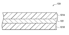
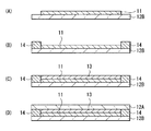
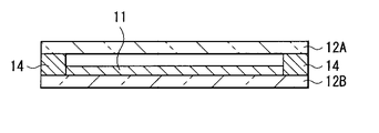
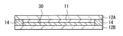
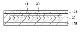
- FIG. 1 shows a cross-sectional structure of a phosphor sheet (color conversion sheet) 10 according to an embodiment of the present invention.
- the phosphor sheet 10 is used by being disposed immediately above a light source such as a blue light emitting diode, for example, and a phosphor layer (color conversion layer) 11 that converts part of blue light from the light source into another color light. Is sealed with a pair of sealing sheets 12A and 12B. Sealing sheet 12A, 12B is bonded together by the 1st bonding layer 13 and the 2nd bonding layer 14 so that the fluorescent substance layer 11 may be pinched
- the phosphor layer 11 converts part of the incident color light into color light in a longer wavelength range.
- the phosphor layer 11 includes, for example, at least one fluorescent material that is excited by blue light and emits green light, red light, or yellow light.
- fluorescent materials for yellow conversion include (Y, Gd) 3 (Al, Ga) 5 O 12 : Ce 3+ (common name YAG: Ce 3+ ), ⁇ -SiAlON: Eu 2+, and the like.
- Examples of the fluorescent material for yellow or green conversion include (Ca, Sr, Ba) 2 SiO 4 : Eu 2+ .
- Examples of the green conversion fluorescent material include SrGa 2 S 4 : Eu 2+ , ⁇ -SiAlON: Eu 2+ , and Ca 3 Sc 2 Si 3 O 12 : Ce 3+ .
- Examples of the red-converted fluorescent material include (Ca, Sr, Ba) S: Eu 2+ , (Ca, Sr, Ba) 2 Si 5 N 8 : Eu 2+ , and CaAlSiN 3 : Eu 2+ .
- the sealing sheets 12A and 12B prevent water vapor from entering the phosphor layer 11, and are disposed so as to face each other on the light incident side and the light emitting side of the phosphor layer 11.
- the configuration of the sealing sheet 12A will be described with reference to FIG.
- the sealing sheet 12A has a structure in which a water vapor barrier layer (water-impermeable layer) 122 is sandwiched between two resin sheets 121A and 121B. That is, the phosphor layer 11 described above is sealed with the water vapor barrier layer 122 with the resin sheet 121A or the resin sheet 121B interposed therebetween.
- resin sheets 121A and 121B include, for example, polyethylene terephthalate (PET), polycarbonate (PC), polymethyl methacrylate (PMMA), polystyrene (PS), polyethylene naphthalate, from the viewpoints of transparency, workability, heat resistance, and the like.
- Thermoplastic resins such as phthalate (PEN), polyethersulfone (PES), and cyclic amorphous polyolefin, polyfunctional acrylates, polyfunctional polyolefins, unsaturated polyesters, epoxy resins, and the like can be used.
- PEN phthalate
- PES polyethersulfone
- cyclic amorphous polyolefin polyfunctional acrylates, polyfunctional polyolefins, unsaturated polyesters, epoxy resins, and the like
- a material which is not easily deteriorated by a blue light emitting diode or a near ultraviolet light emitting diode such as polyethylene terephthalate, polycarbonate, polymethyl methacrylate and polystyrene.
- sealing sheet 12B The same applies to the sealing sheet 12B.
- the water vapor barrier layer 122 is made of a material having a low water vapor transmission rate, for example, an inorganic material such as silicon oxide or silicon nitride, magnesium oxide (MgO), indium oxide, aluminum oxide (Al 2 O 3 ), and tin oxide, It is composed of a single layer or a composite layer made of an organic material such as polyvinyl alcohol, ethylene vinyl alcohol copolymer, polyacrylonitrile, and polyvinylidene chloride. Further, the water vapor transmission rate is preferably 2.0 g / m 2 / day or less, for example. Further, it is preferable to use a material having a low gas permeability such as oxygen in addition to the water vapor permeability.
- an inorganic material such as silicon oxide or silicon nitride, magnesium oxide (MgO), indium oxide, aluminum oxide (Al 2 O 3 ), and tin oxide
- MgO magnesium oxide
- Al 2 O 3 aluminum oxide
- tin oxide tin oxide
- the 1st bonding layer 13 is provided between the light emission surface of the fluorescent substance layer 11, and 12A of sealing sheets, and the 2nd bonding layer 14 is along the outer periphery of the fluorescent substance layer 11, ie, a fluorescent substance layer. It is provided in a frame shape so as to surround 11 planar shapes.
- a 1st bonding layer 13 and the 2nd bonding layer 14 are comprised by the adhesive material which has water vapor
- the 1st bonding layer 13 is arrange
- the second bonding layer 14 may be transparent or opaque, but it is preferable to use a material having a high water vapor barrier property.
- Such a phosphor sheet 10 can be manufactured, for example, as follows.
- sealing sheets 12A and 12B having a configuration as shown in FIG. 2 are prepared. That is, the water vapor barrier layer 122 made of the above-described material is formed on the resin sheet 121A made of the above-mentioned material by various film forming methods, for example, vapor deposition or sputtering. When an organic material is used as the water vapor barrier layer 122, the film may be formed by coater coating, spray coating, or the like. Subsequently, another resin sheet 121B is overlaid on the formed water vapor barrier layer 122, and the water vapor barrier layer 122 is sealed between the resin sheets 121A and 121B.
- various film forming methods for example, vapor deposition or sputtering.
- the film may be formed by coater coating, spray coating, or the like.
- another resin sheet 121B is overlaid on the formed water vapor barrier layer 122, and the water vapor barrier layer 122 is sealed between the resin sheets 121A and 121B.
- the second bonding layer 14 made of the above-described material is applied and formed on the peripheral edge of the produced sealing sheet 12B.
- a region (not shown; hereinafter referred to as a gate portion) where the second bonding layer 14 is not formed is provided in the peripheral portion of the sealing sheet 12B.
- another sealing sheet 12 ⁇ / b> A is overlaid and bonded to the sealing sheet 12 ⁇ / b> B from above the second bonding layer 14.
- the phosphor layer 11 made of the above-described material is applied and formed on the surface of the sealing sheet 12B through the gate portion.
- the first bonding layer 13 made of the above-described material is injected from the gate portion into the gap between the formed phosphor layer 11 and the sealing sheet 12A and bonded.
- the phosphor sheet 10 shown in FIG. 1 is completed.
- the phosphor sheet 10 for example, when blue light is incident from below the sealing sheet 12 ⁇ / b> B, part of the blue light in the phosphor layer 11 is converted into light in other wavelength ranges, such as red light and green light. Then, the light is emitted upward of the phosphor layer 11. On the other hand, the other part of the blue light incident on the phosphor layer 11 is emitted without being color-converted. In this way, each color light emitted from the phosphor layer 11 sequentially passes through the first bonding layer 13 and the sealing sheet 12A, and becomes, for example, white light by color mixing and is emitted from above the sealing sheet 12A. .
- the phosphor layer 11 as described above is sealed by the sealing sheets 12A and 12B having the water vapor barrier layer 122, thereby preventing water vapor from entering the phosphor layer 11 and emitting light. Degradation of characteristics such as efficiency can be suppressed. This is particularly effective when the phosphor layer 11 is made of a sulfide-based or oxysulfide-based fluorescent material that is fragile to water vapor.
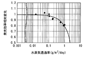
- FIG. 4 shows the change in the luminous efficiency of the phosphor layer 11 with respect to the water vapor transmission rate of the water vapor barrier layer 122.
- the phosphor sheet 10 is manufactured using a phosphor material generally considered to be fragile to water vapor, and is left in an environment of 85 ° C. and 90% RH for 500 hours.
- This is an investigation of changes in luminous efficiency.
- relative changes with an initial luminous efficiency of 1 are shown.
- the lower the water vapor transmission rate that is, the lower the water vapor barrier property, the more the light emission efficiency decreases.
- the acceleration coefficient under the above environment is generally set to 70 or more, which corresponds to deterioration when used in an actual environment for 35000 hours or more.
- the time required to reduce the luminance by half is 30000 hours or more, which is a condition for guaranteeing reliability. Therefore, if the water vapor transmission rate is 2 g / m 2 / day or less, the reliability condition as described above can be exceeded.
- the water vapor barrier layer 122 prevents water vapor from entering the phosphor layer 11, it easily causes a chemical reaction with the phosphor layer 11 itself, and the phosphor layer 11 deteriorates due to this chemical reaction. There is a possibility that the characteristics may be deteriorated.
- the phosphor layer 11 is sealed with the water vapor barrier layer 122 by the sealing sheets 12A and 12B with the resin sheet 121A or the resin sheet 121B interposed therebetween. There is no direct contact with the barrier layer 122. Therefore, a chemical reaction is less likely to occur between the phosphor layer 11 and the water vapor barrier layer 122.
- the water vapor barrier layer 122 is sandwiched between the two resin sheets 121A and 121B in the sealing sheets 12A and 12B, the water vapor barrier layer 122 is not exposed to the outside. This will ensure the weather resistance and prevent mechanical damage. Thereby, the surface state of the water vapor barrier layer 122 is improved, the range of selection of the printing process of the phosphor layer 11 and the bonding layer material is expanded, and the productivity is improved.
- the phosphor layer 11 converts a part of the blue light from the light source into another color light and emits it, and the other part of the blue light is emitted without color conversion.
- white light can be obtained by mixing light of each color.
- the phosphor layer 11 is sealed with sealing sheets 12A and 12B, and the sealing sheets 12A and 12B have a resin sheet 121A (or resin sheet 121B) and a water vapor barrier layer 122 from the phosphor layer 11 side, respectively. Therefore, deterioration of the phosphor layer 11 can be suppressed.
- the phosphor sheet 10 as described above can be applied to the display device 1 (light emitting device 3) as shown in FIG. 5, for example.
- the display device 1 includes a light emitting device 3 as a backlight composed of a light source unit 2 and a phosphor sheet 10 and a display panel 4 driven based on image data. Between the light emitting device 3 and the display panel 4, various optical functional films such as a diffusion plate 5, a diffusion film 6, a lens film (light collecting member) 7, and a reflective polarizing film 8 are arranged in this order from the light emitting device 3 side. Has been placed.
- the light source unit 2 has a plurality of blue LEDs 21 arranged on the substrate 20 and performs surface emission as a whole.
- the phosphor sheet 10 is disposed immediately above the light source unit 2.
- the display panel 4 includes, for example, a liquid crystal layer (both shown in the figure) between a TFT substrate on which a pixel electrode, a TFT (Thin Film Transistor) element, and the like are formed and a counter substrate on which a counter electrode, a color filter, and the like are formed. (Not shown) is sealed. Polarizing plates (not shown) are bonded to the light incident side and the light emitting side of the display panel 4 so that their polarization axes are orthogonal to each other.
- the diffusion plate 5 and the diffusion film 6 diffuse incident light and make the intensity distribution uniform, and correspond to the light diffusion member of the present invention.
- the lens film 7 includes a plurality of prism-shaped protrusions arranged in parallel, and has a function of collecting incident light.
- the reflective polarizing film 8 transmits one polarized light and reflects the other polarized light downward (to the light emitting device 3 side) for reuse.
- the reflective polarizing film 8 is provided to increase the light utilization efficiency.
- the blue light emitted from the blue LED 21 emits white light as described above by the phosphor sheet 10.
- the white light emitted from the light emitting device 3 is diffused by the diffusion plate 5 and the diffusion film 6, then collected by the lens film 7, and passes through the reflective polarizing film 8 to irradiate the display panel 4.
- the light emitted in this way is modulated by the display panel 4 based on the image data, and image display is performed.
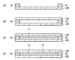
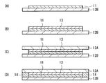
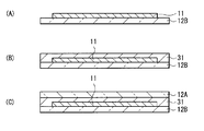
- FIG. 6 (Modification 1) 6A to 6D show the method for manufacturing the phosphor sheet 10 according to Modification 1 in the order of steps.
- the phosphor sheet 10 can also be manufactured as follows. First, as shown to FIG. 6 (A), the fluorescent substance layer 11 is apply
- (Modification 2) 7A to 7D show the manufacturing method of the phosphor sheet 10 according to Modification 2 in the order of steps.
- the phosphor sheet 10 can also be manufactured as follows. First, as shown to FIG. 7 (A), the fluorescent substance layer 11 is apply
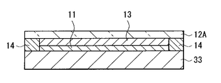
- FIG. 8 shows a cross-sectional structure of a phosphor sheet according to Modification 3.
- the first bonding layer 13 is not provided, and the phosphor layer 11 is hermetically sealed only by the second bonding layer 14 between the sealing sheets 12A and 12B. Except for this, the configuration is the same as in the above embodiment.
- one sealing sheet 12A and the fluorescent substance layer 11 do not necessarily need to adhere
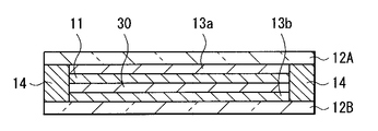
- FIG. 9 illustrates a cross-sectional structure of the phosphor sheet according to the fourth modification.
- the phosphor layer 11 is formed on the base film 30, and the first bonding layer 13a and the base film 30 are sealed between the phosphor layer 11 and the sealing sheet 12A. Except that the 1st bonding layer 13b is provided between the sheet
- the base film 30 is made of, for example, polyethylene terephthalate.
- the 1st bonding layers 13a and 13b are comprised with the material similar to the 1st bonding layer 13 of the said embodiment.
- FIG. 10 illustrates a cross-sectional structure of the phosphor sheet according to the fifth modification.
- the phosphor sheet of Modification Example 5 is not provided with the first bonding layers 13a and 13b and is hermetically sealed only by the second bonding layer 14, and the phosphor according to Modification Example 4 described above. It has the same configuration as the seat. Thus, if the airtightness between the sealing sheets 12A and 12B is ensured by the second bonding layer 14, the sealing sheet 12A and the phosphor layer 11, and the sealing sheet 12B and the base film 30 are respectively used. , It is not necessarily bonded.
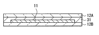
- FIG. 11 shows a cross-sectional structure of a phosphor sheet according to Modification 6.
- the phosphor sheet of Modification 6 is provided with a bonding layer 31 so as to cover the entire phosphor layer 11 disposed on the sealing sheet 12B, and the phosphor layer 11 is between the sealing sheets 12A and 12B. It becomes the structure airtightly sealed only by the bonding layer 31.
- the bonding layer 31 is comprised with the material similar to the 1st bonding layer 13 of the said embodiment, it is preferable that it has sufficient water vapor
- Such a phosphor sheet can be manufactured, for example, as follows. First, as shown to FIG. 12 (A), the fluorescent substance layer 11 is apply
- the bonding layer 31 may be continuously formed over the entire surface of the sealing sheets 12A and 12B. This simplifies the manufacturing process.
- FIG. 13A shows an enlarged view of the vicinity of the edge seal portion 31A of the bonding layer 31, and FIG. 13B shows a view of the phosphor layer 11 and the edge seal portion 31A as viewed from above.
- the peripheral portion (edge seal portion 31A) of the bonding layer 31 protects the phosphor layer 11 from the side surface.
- the deterioration of the phosphor layer 11 proceeds mainly by the intrusion of oxygen or the like from the upper surface and the lower surface of the phosphor layer 11, but in the vicinity of the side surface of the phosphor layer 11, the intrusion from the side surface in addition to the upper and lower surfaces cannot be ignored.
- the edge seal portion 31 ⁇ / b> A contributes particularly to suppression of deterioration due to intrusion of oxygen or the like from the side surface of the phosphor layer 11.
- FIG. 14 shows the emission intensity ratio (emission intensity at measurement point B / emission intensity at measurement point A) at each width X.
- the width of the edge seal portion 31A is not limited to 2 mm or more. This is because the same effects as described above can be obtained even when the thickness is less than 2 mm depending on the combination of the phosphors and the materials of the bonding layer.
- FIG. 15 illustrates a cross-sectional structure of a phosphor sheet according to Modification 7.
- the phosphor layer 11 is formed on the base film 30 of Modification Examples 4 and 5, and the whole is surrounded by the bonding layer 32, and between the sealing sheets 12A and 12B. Is hermetically sealed.
- the bonding layer 32 is made of the same material as that of the bonding layer 31 of Modification 6 described above. As described above, the entire base film 30 on which the phosphor layer 11 is formed may be sealed between the sealing sheets 12A and 12B by the bonding layer 32.
- FIG. 16 shows a cross-sectional structure of a phosphor sheet according to Modification 8.
- the phosphor sheet of Modification 8 has the same configuration as that of the phosphor sheet 10 of the above embodiment except that the optical functional layer 33 is disposed instead of the one sealing sheet 12B.
- the optical functional layer 33 is, for example, various optical films such as the diffusion plate 5, the diffusion film 6, the lens film 7, and the reflective polarizing film 8 in the display device 1 described above.
- the phosphor layer 11 is formed on one surface of such an optical function layer 33, and the sealing sheet 12 ⁇ / b> A is bonded thereon by the first bonding layer 13 and the second bonding layer 14. ing.
- the optical functional layer 33 has a sufficient water vapor barrier property. Use of such a phosphor sheet is advantageous for reducing the thickness of the light emitting device or the display device.
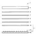
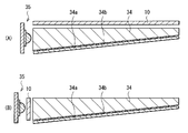
- Modification 9 17A and 17B illustrate a cross-sectional structure of a light-emitting device according to Modification Example 9.
- FIG. The light emitting device of Modification 9 uses a light guide plate 34 that propagates light from a blue LED 35 provided on the side surface and emits light upward as a light source unit.
- a light reflecting material 34a and a light diffusing material 34b are provided on the bottom surface of the light guide plate 34.
- the light source of the phosphor sheet 10 is not limited to the one in which a plurality of blue LEDs are arranged on the substrate as described above, and even if the light guide plate 34 is used as in this modification. Good.
- the phosphor sheet 10 may be disposed so as to face the light emitting side surface of the light guide plate 34 as shown in FIG. 17 (A), as shown in FIG. 17 (B).
- the light guide plate 34 may be disposed to face the light incident side surface.
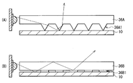
- a phosphor layer may be formed on the light incident surface or the light emitting surface of the light guide plate 34, and this may be covered with a sealing sheet. Further, the phosphor sheet 10 may be disposed on the bottom side of the light guide plate 34.
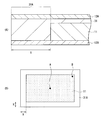
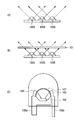
- FIG. 18A shows a specific configuration when a phosphor sheet is disposed on the bottom surface side of the light guide plate.
- a plurality of grooves 36A1 are formed on the bottom surface of the light guide plate 36A as a light extraction process.
- the phosphor sheet 10 is provided below the plurality of grooves 36A1. Is arranged.
- the light propagating through the light guide plate 36A is emitted above the light guide plate 36A by breaking the total reflection condition (below the critical angle) by the groove 36A1.
- the total reflection condition is broken in the groove 36A1
- the blue light passes through the phosphor sheet 10 and undergoes color conversion.
- the light extraction processing in the light guide plate 36A is not limited to the groove 36A1 as described above.
- a light guide plate 36B having a plurality of dots 36B1 printed on the bottom surface may be used.
- FIG. 19 illustrates a schematic configuration of a light emitting device according to Modification Example 10.
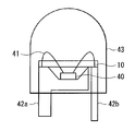
- the light emitting device of Modification 10 is, for example, a blue light emitting diode, in which the phosphor sheet 10 is disposed immediately above the light emitting unit 40.
- the light emitting unit 40 is electrically connected to the cathode frame 42 a and the anode frame 42 b by wire bonds 41.
- the light emitting unit 40 and the phosphor sheet 10 are sealed with an exterior cap 43. In this way, the phosphor sheet 10 may be disposed immediately above the light emitting unit 40 of the blue light emitting diode.
- Modification 11 20A and 20B show a cross-sectional structure of a display device according to the eleventh modification.
- the position where the phosphor sheet 10 is installed is different from the display device 1 of the above embodiment. That is, the phosphor sheet 10 is provided between the diffusion plate 5 and the diffusion film 6 (FIG. 20A) or between the diffusion film 6 and the lens film 7 (FIG. 20B).
- the phosphor sheet 10 is not limited to the position directly above the light source unit 2, and may be disposed at any position between the light source unit 2 and the reflective polarizing film 8.
- the diffusion plate 5 and the diffusion film 6 are arranged as shown in FIG. 20A or as shown in FIG. It is good to arrange between. Therefore, the arrangement configuration shown in FIG. 20A is preferable in which both the viewing angle dependency of the chromaticity in the emitted light and the emission angle dependency from the light source can be minimized.
- the configuration using a blue light emitting diode as a light source has been described as an example.
- the present invention is not limited to this, and a light source that emits colored light in a relatively short wavelength region, for example, a near ultraviolet light emitting diode may be used.
- the color conversion layer has (Ca, Sr, Ba) 2 SiO 4 : Eu 2+ , BAM: Eu 2+ , Mn 2+ and ⁇ -SiAlON: Eu 2 as a fluorescent material for green conversion or yellow conversion. + Can be used.
- Y 2 O 2 S: Eu 3+ , La 2 O 2 S: Eu 3+ , (Ca, Sr, Ba) 2 Si 5 N 8 : Eu 2+ , CaAlSiN 3 : Eu 2+ , LiEuW 2 O 8 , Ca (Eu, La) 4 Si 3 O 13 , Eu 2 W 2 O 9 , (La, Eu) 2 W 3 O 12 , (Ca, Sr, Ba) 3 MgSi 2 O 8 : Eu 2+ , Mn 2+ , CaTiO 3 : Pr 3+ , Bi 3+ and the like can be used.
- BAM Eu 2+
- (Ca, Sr, Ba) 5 (PO 4 ) 3 Cl: Eu 2+, or the like can be used as a fluorescent material for blue conversion.
- the structure which consists of the light source part 2 and the fluorescent substance sheet 10 was mentioned as an example as a light-emitting device, it is not limited to this, For example, other light emission side of the fluorescent substance sheet 10 is provided.
- An optical functional layer for example, the diffusing plate 5, the diffusing film 6, the lens film 7 and the reflective polarizing film 8 as described above may be provided. That is, it is only necessary to include the light source unit and the phosphor sheet.
- the structure using the liquid crystal panel as the display panel of the display device of the present invention has been described as an example.
- the present invention is not limited to this and can be applied to other display devices. is there.
Abstract
Description
上記のような蛍光体シート10は、例えば図5に示したような表示装置1(発光装置3)に適用することができる。
図6(A)~(D)は、変形例1に係る蛍光体シート10の製造方法について工程順に表したものである。蛍光体シート10は、次のようにして製造することも可能である。まず図6(A)に示したように、封止シート12B上の周縁部を除いた領域に蛍光体層11を塗布形成する。続いて、図6(B)に示したように、封止シート12B上の周縁部に、すなわち蛍光体層11の平面形状を囲むように第2貼合層14を形成する。こののち、図6(C)に示したように、蛍光体層11の全面を覆うように第1貼合層13を形成する。この上から、図6(D)に示したように、封止シート12Aを貼り合わせることにより、蛍光体シート10を完成する。
図7(A)~(D)は、変形例2に係る蛍光体シート10の製造方法について工程順に表したものである。蛍光体シート10は、次のようにして製造することも可能である。まず図7(A)に示したように、封止シート12B上の周縁部を除いた領域に蛍光体層11を塗布形成する。続いて、図7(B)に示したように、蛍光体層11の光出射側の全面を覆うように第1貼合層13を形成する。次いで、図7(C)に示したように、第1貼合層13の上から封止シート12Aを貼り合わせる。最後に、図7(D)に示したように、封止シート12Aと封止シート12Bとの間を、外側から封止するように第2貼合層14を形成することにより、蛍光体シート10を完成する。
図8は、変形例3に係る蛍光体シートの断面構造を表すものである。変形例3の蛍光体シートは、第1貼合層13が設けられておらず、蛍光体層11が封止シート12A,12Bの間に第2貼合層14のみによって気密封止されていること以外は、上記実施の形態と同様の構成となっている。このように、第2貼合層14によって封止シート12A,12Bとの間の気密性が確保されていれば、一方の封止シート12Aと蛍光体層11とは必ずしも接着されていなくともよい。これにより、低コスト化や製造プロセスの簡易化を図ることができる。
図9は、変形例4に係る蛍光体シートの断面構造を表すものである。変形例4の蛍光体シートは、蛍光体層11が基材フィルム30上に形成され、蛍光体層11と封止シート12Aとの間に第1貼合層13a、基材フィルム30と封止シート12Bとの間に第1貼合層13bが設けられていること以外は、上記実施の形態と同様の構成となっている。基材フィルム30は、例えばポリエチレンテレフタレートなどにより構成されている。第1貼合層13a,13bは、上記実施の形態の第1貼合層13と同様の材料により構成されている。このように蛍光体層11を基材フィルム30上に形成することにより、蛍光層11の反りを防止することができると共に、蛍光体層11の塗布プロセスが容易となる。
図10は、変形例5に係る蛍光体シートの断面構造を表すものである。変形例5の蛍光体シートは、第1貼合層13a,13bが設けられておらず、第2貼合層14のみによって気密封止されていること以外は、上記変形例4に係る蛍光体シートと同様の構成となっている。このように、第2貼合層14によって封止シート12A,12B間の気密性が確保されていれば、封止シート12Aと蛍光体層11、および封止シート12Bと基材フィルム30はそれぞれ、必ずしも接着されていなくともよい。
図11は、変形例6に係る蛍光体シートの断面構造を表すものである。変形例6の蛍光体シートは、封止シート12B上に配置された蛍光体層11全体を覆うようにして貼合層31が設けられており、蛍光体層11が封止シート12A,12B間に貼合層31のみによって気密封止された構成となっている。貼合層31は、上記実施の形態の第1貼合層13と同様の材料により構成されるが、十分な水蒸気バリア性を有していることが好ましい。
図15は、変形例7に係る蛍光体シートの断面構造を表すものである。変形例7の蛍光体シートは、蛍光体層11が上記変形例4,5の基材フィルム30上に形成されており、これら全体が貼合層32によって包囲され、封止シート12A,12B間に気密封止されている。貼合層32は、上記変形例6の貼合層31と同様の材料により構成されている。このように、蛍光体層11を形成した基材フィルム30全体を貼合層32によって、封止シート12A,12B間に封止してもよい。
図16は、変形例8に係る蛍光体シートの断面構造を表すものである。変形例8の蛍光体シートは、一方の封止シート12Bの代わりに光学機能層33を配置したこと以外は、上記実施の形態の蛍光体シート10と同様の構成となっている。光学機能層33は、例えば上述の表示装置1における拡散板5、拡散フィルム6、レンズフィルム7および反射型偏光フィルム8などの各種光学フィルムである。本変形例では、このような光学機能層33の一面に蛍光体層11が形成されており、この上に第1貼合層13および第2貼合層14によって封止シート12Aが貼り合わせられている。但し、この場合、光学機能層33が十分な水蒸気バリア性を有していることが好ましい。このような蛍光体シートを用いることで、発光装置もしくは表示装置の薄型化に有利となる。
図17(A),(B)は、変形例9に係る発光装置の断面構造を表すものである。変形例9の発光装置は、光源部として、側面に設けられた青色LED35からの光を伝搬させ上方に向けて面発光を行う導光板34を用いたものである。導光板34の底面には光反射材34aおよび光拡散材34bが設けられている。このように、蛍光体シート10の光源としては、上述したような基板上に複数の青色LEDを配置したものに限定されず、本変形例のように導光板34を用いたものであってもよい。また、この場合、蛍光体シート10は、図17(A)に示したように導光板34の光出射側の面に対向させて配置してもよく、図17(B)に示したように導光板34の光入射側の面に対向させて配置してもよい。
図19は、変形例10に係る発光装置の概略構成を表すものである。変形例10の発光装置は、例えば青色発光ダイオードであり、発光部40の直上に蛍光体シート10が配置されたものである。発光部40は、ワイヤボンド41により陰極フレーム42aおよび陽極フレーム42bに電気的に接続されている。発光部40および蛍光体シート10は、外装キャップ43により封止されている。このように青色発光ダイオードの発光部40の直上に蛍光体シート10を配置してもよい。
図20(A),(B)は、変形例11に係る表示装置の断面構造を表すものである。変形例11に係る表示装置では、蛍光体シート10の設置される位置が上記実施の形態の表示装置1と異なっている。すなわち、蛍光体シート10が、拡散板5と拡散フィルム6との間(図20(A))、もしくは拡散フィルム6とレンズフィルム7との間(図20(B))に設けられている。このように、蛍光体シート10は、光源部2の直上に限らず、光源部2と反射型偏光フィルム8との間のいずれの位置に配置されていてもよい。但し、蛍光体シート10より出射される光の色度の視野角依存性を最小にするためには、図5に示したように光源部2の直上に配置するか、あるいは図20(A)に示したように拡散板5と拡散フィルム6との間に配置するのがよい。一方、出射光の色度のLED光源からの放射角依存性を最小にするためには、図20(A)の配置構成もしくは図20(B)に示したように拡散フィルム6とレンズフィルム7との間に配置するのがよい。よって、出射光における色度の視野角依存性および光源からの放射角依存性のいずれも最小とすることのできる図20(A)の配置構成が好ましい。
Claims (17)
- 光源部と、
前記光源部から発せられた色光の少なくとも一部を他の色光に変換する色変換層と、
前記色変換層を封止する不透水性の封止シートと
を備えた発光装置。 - 前記封止シートは、前記色変換層の側から樹脂シートと不透水層とを有する
請求項1に記載の発光装置。 - 前記封止シートは、前記樹脂シートと他の樹脂シートとにより前記不透水層を挟み込んで構成されている
請求項2に記載の発光装置。 - 前記封止シートが一対設けられ、
前記色変換層を間に挟んで前記一対の封止シート同士を貼り合わせる貼合層をさらに含む
請求項1に記載の発光装置。 - 前記貼合層は、前記色変換層全体を覆うように設けられている
請求項4に記載の発光装置。 - 前記光源部は、青色(B:Blue)の光を発する青色発光ダイオードを含む
請求項1に記載の発光装置。 - 前記色変換層は、前記青色光の一部を他の色光に変換することにより、全体として白色光を出射する
請求項6に記載の発光装置。 - 前記光源部は、前記色変換層の表面に平行な方向に沿って配列された複数の発光ダイオードを含む
請求項1に記載の発光装置。 - 前記光源部は、
発光ダイオードと、
前記発光ダイオードから発せられた光を伝搬させて面発光を行う導光板と
を含む
請求項1に記載の発光装置。 - 前記導光板の光入射面もしくは光出射面上に前記色変換層が形成され、前記色変換層上を前記封止シートが覆っている
請求項9に記載の発光装置。 - 前記色変換層は、蛍光材料を含んで構成されている
請求項1に記載の発光装置。 - 光源部から発せられた色光の少なくとも一部を他の色光に変換する色変換層と、
前記色変換層を封止する不透水性の封止シートと
を備えた色変換シート。 - 光源部と、
画像データに基づいて駆動される表示パネルと、
前記光源部から発せられた色光の少なくとも一部を他の色光に変換して前記表示パネルに導く色変換層と、
前記色変換層を封止する不透水性の封止シートと
を備えた表示装置。 - 前記光源部と前記表示パネルとの間に、前記光源部の側から順に光拡散部材と、集光部材とが設けられている
請求項13に記載の表示装置。 - 前記光源部と前記光拡散部材との間に、前記色変換層および前記封止シートが設けられている
請求項14に記載の表示装置。 - 前記光拡散部材と前記集光部材との間に、前記色変換層および前記封止シートが設けられている
請求項14に記載の表示装置。 - 前記光拡散部材は、前記光源部の側から順に光拡散フィルムと光拡散板とを含み、
前記光拡散フィルムと前記光拡散板との間に、前記色変換層および前記封止シートが設けられている
請求項14に記載の表示装置。
Priority Applications (2)
| Application Number | Priority Date | Filing Date | Title |
|---|---|---|---|
| US12/988,557 US8514350B2 (en) | 2008-04-25 | 2009-04-20 | Light emitting device, display device, and color conversion sheet |
| CN200980114422.9A CN102016403B (zh) | 2008-04-25 | 2009-04-20 | 发光装置、显示装置和色彩转换片 |
Applications Claiming Priority (4)
| Application Number | Priority Date | Filing Date | Title |
|---|---|---|---|
| JP2008115719 | 2008-04-25 | ||
| JP2008-115719 | 2008-04-25 | ||
| JP2009031317A JP5418762B2 (ja) | 2008-04-25 | 2009-02-13 | 発光装置および表示装置 |
| JP2009-031317 | 2009-02-13 |
Publications (1)
| Publication Number | Publication Date |
|---|---|
| WO2009131092A1 true WO2009131092A1 (ja) | 2009-10-29 |
Family
ID=41216825
Family Applications (1)
| Application Number | Title | Priority Date | Filing Date |
|---|---|---|---|
| PCT/JP2009/057843 WO2009131092A1 (ja) | 2008-04-25 | 2009-04-20 | 発光装置、表示装置および色変換シート |
Country Status (5)
| Country | Link |
|---|---|
| US (1) | US8514350B2 (ja) |
| JP (1) | JP5418762B2 (ja) |
| CN (1) | CN102016403B (ja) |
| TW (1) | TWI508620B (ja) |
| WO (1) | WO2009131092A1 (ja) |
Cited By (6)
| Publication number | Priority date | Publication date | Assignee | Title |
|---|---|---|---|---|
| WO2013035485A1 (ja) * | 2011-09-05 | 2013-03-14 | 日本電気硝子株式会社 | 発光デバイス用セル、発光デバイス及び発光デバイス用セルの製造方法 |
| WO2014000326A1 (zh) * | 2012-06-28 | 2014-01-03 | 深圳市华星光电技术有限公司 | 荧光粉基板的制作方法及用该荧光粉基板的液晶模组 |
| WO2017010394A1 (ja) * | 2015-07-10 | 2017-01-19 | 富士フイルム株式会社 | 積層フィルムおよび積層フィルムの製造方法 |
| CN106536197A (zh) * | 2014-07-24 | 2017-03-22 | 凸版印刷株式会社 | 层叠膜及层叠体、以及波长转换片材、背光单元及电致发光单元 |
| EP3202873A1 (en) * | 2010-05-10 | 2017-08-09 | Dexerials Corporation | Green-emitting phosphor particles, method for manufacturing green-emitting phosphor particles, color conversion sheet, light-emitting device, and image display device assembly |
| JP2018018973A (ja) * | 2016-07-28 | 2018-02-01 | 富士フイルム株式会社 | バックライト用フィルム |
Families Citing this family (68)
| Publication number | Priority date | Publication date | Assignee | Title |
|---|---|---|---|---|
| US11198270B2 (en) | 2008-12-30 | 2021-12-14 | Nanosys, Inc. | Quantum dot films, lighting devices, and lighting methods |
| EP3258167A3 (en) * | 2009-12-08 | 2018-04-18 | 3M Innovative Properties Co. | Optical constructions incorporating a light guide and low refractive index films |
| JP5238753B2 (ja) * | 2010-05-31 | 2013-07-17 | 株式会社日立製作所 | 照明装置 |
| KR101154368B1 (ko) * | 2010-09-27 | 2012-06-15 | 엘지이노텍 주식회사 | 광변환부재 제조방법 및 그 제조방법으로 제조된 광변환부재를 포함하는 백라이트 유닛 |
| CN104932051A (zh) | 2010-11-10 | 2015-09-23 | 纳米系统公司 | 量子点薄膜、照明器件及照明方法 |
| KR101199064B1 (ko) * | 2011-01-21 | 2012-11-07 | 엘지이노텍 주식회사 | 광 변환 부재, 이를 포함하는 표시장치 및 이의 제조방법 |
| KR101210066B1 (ko) | 2011-01-31 | 2012-12-07 | 엘지이노텍 주식회사 | 광 변환 부재 및 이를 포함하는 표시장치 |
| KR20120107793A (ko) * | 2011-03-22 | 2012-10-04 | 엘지이노텍 주식회사 | 표시장치 및 광 변환 부재 |
| JP5777705B2 (ja) * | 2011-04-20 | 2015-09-09 | 株式会社エルム | 発光装置及びその製造方法 |
| KR101210180B1 (ko) | 2011-04-21 | 2012-12-07 | 엘지이노텍 주식회사 | 광학 부재 및 이의 제조방법 |
| KR101792882B1 (ko) * | 2011-06-23 | 2017-11-20 | 엘지이노텍 주식회사 | 광학 부재 및 이를 포함하는 표시장치 |
| JP5373859B2 (ja) * | 2011-07-05 | 2013-12-18 | デクセリアルズ株式会社 | 照明装置 |
| KR20130009020A (ko) | 2011-07-14 | 2013-01-23 | 엘지이노텍 주식회사 | 광학 부재, 이를 포함하는 표시장치 및 이의 제조방법 |
| KR101305696B1 (ko) | 2011-07-14 | 2013-09-09 | 엘지이노텍 주식회사 | 표시장치 및 광학 부재 |
| KR101262541B1 (ko) | 2011-07-18 | 2013-05-08 | 엘지이노텍 주식회사 | 표시장치 |
| KR101893494B1 (ko) | 2011-07-18 | 2018-08-30 | 엘지이노텍 주식회사 | 광학 부재 및 이를 포함하는 표시장치 |
| KR101241549B1 (ko) | 2011-07-18 | 2013-03-11 | 엘지이노텍 주식회사 | 광학 부재, 이를 포함하는 표시장치 및 이의 제조방법 |
| KR101262520B1 (ko) * | 2011-07-18 | 2013-05-08 | 엘지이노텍 주식회사 | 광학 부재 및 이를 포함하는 표시장치 |
| KR101294415B1 (ko) | 2011-07-20 | 2013-08-08 | 엘지이노텍 주식회사 | 광학 부재 및 이를 포함하는 표시장치 |
| JP2014199831A (ja) * | 2011-08-12 | 2014-10-23 | シャープ株式会社 | 発光装置、蛍光体シート、及びバックライトシステム、及び発光装置の製造方法 |
| KR101878270B1 (ko) * | 2011-09-15 | 2018-07-13 | 엘지이노텍 주식회사 | 광여기 판을 포함하는 조명 장치 및 광여기 테이프 |
| KR101251815B1 (ko) | 2011-11-07 | 2013-04-09 | 엘지이노텍 주식회사 | 광학 시트 및 이를 포함하는 표시장치 |
| KR101338695B1 (ko) | 2012-04-27 | 2013-12-06 | 엘지이노텍 주식회사 | 표시 장치, 광 변환 부재 및 광 변환 부재 제조 방법 |
| KR101877493B1 (ko) * | 2012-05-04 | 2018-07-13 | 엘지이노텍 주식회사 | 광 변환 부재 및 광 변환 부재 제조 방법 |
| WO2014006501A1 (en) * | 2012-07-03 | 2014-01-09 | Yosi Shani | Planar remote phosphor illumination apparatus |
| JP6636324B2 (ja) * | 2012-07-05 | 2020-01-29 | シグニファイ ホールディング ビー ヴィSignify Holding B.V. | ルミネッセンス材料を含む層のスタック、ランプ、照明器具及びそのような層のスタックを製造する方法 |
| JP2014096419A (ja) * | 2012-11-07 | 2014-05-22 | Stanley Electric Co Ltd | 光電子デバイス |
| US9543478B2 (en) * | 2012-11-07 | 2017-01-10 | Koninklijke Philips N.V. | Light emitting device including a filter and a protective layer |
| JP2013077825A (ja) * | 2012-11-26 | 2013-04-25 | Dexerials Corp | 緑色発光蛍光体粒子、色変換シート、発光装置及び画像表示装置組立体 |
| JP5796038B2 (ja) | 2013-06-18 | 2015-10-21 | デクセリアルズ株式会社 | 蛍光体シート |
| JP6217187B2 (ja) * | 2013-07-03 | 2017-10-25 | ソニー株式会社 | 発光装置および表示装置 |
| KR102108994B1 (ko) * | 2013-08-30 | 2020-05-12 | 삼성전자주식회사 | 광 변환 소자 및 그 제조 방법, 그리고 이를 포함하는 광원 유닛 |
| KR101438509B1 (ko) * | 2013-12-30 | 2014-09-12 | (주)스프린터 | 블루led 광에 대한 백화(白化)부를 구비한 사인시트 및 이를 이용한 디스플레이 장치 |
| JP5820894B2 (ja) | 2014-02-21 | 2015-11-24 | デクセリアルズ株式会社 | 封止テープ、蛍光体シート、及び蛍光体シートの製造方法 |
| WO2015138495A1 (en) * | 2014-03-11 | 2015-09-17 | Osram Sylvania Inc. | Light converter assemblies with enhanced heat dissipation |
| JP6330902B2 (ja) * | 2014-04-04 | 2018-05-30 | 凸版印刷株式会社 | 波長変換シート及びバックライトユニット |
| CN103928591A (zh) * | 2014-04-18 | 2014-07-16 | 深圳市华星光电技术有限公司 | 一种荧光条及使用荧光条的led封装模组 |
| KR20150145798A (ko) * | 2014-06-19 | 2015-12-31 | 삼성디스플레이 주식회사 | 백라이트 어셈블리 및 그를 포함하는 표시장치 |
| KR102204953B1 (ko) * | 2014-06-25 | 2021-01-19 | 삼성디스플레이 주식회사 | 형광 시트 및 이를 포함하는 라이트 유닛과 액정 표시 장치 |
| KR20160038325A (ko) * | 2014-09-30 | 2016-04-07 | 코닝정밀소재 주식회사 | 색변환용 기판, 그 제조방법 및 이를 포함하는 디스플레이 장치 |
| JP6572906B2 (ja) * | 2014-11-14 | 2019-09-11 | 凸版印刷株式会社 | 光学バリアフィルム、色変換フィルム、及びバックライトユニット |
| KR102260013B1 (ko) * | 2014-12-10 | 2021-06-04 | 삼성디스플레이 주식회사 | 표시 장치 및 이의 제조 방법 |
| EP3263973A4 (en) * | 2015-02-25 | 2018-10-17 | Sharp Kabushiki Kaisha | Illuminating device, display device, and television receiving device |
| US9870739B2 (en) * | 2015-05-13 | 2018-01-16 | Apple Inc. | Display with backlight and temperature color compensation |
| JP6433592B2 (ja) | 2015-06-17 | 2018-12-05 | 富士フイルム株式会社 | 積層フィルムおよび積層フィルムの製造方法 |
| KR102016407B1 (ko) | 2015-06-18 | 2019-09-02 | 후지필름 가부시키가이샤 | 적층 필름 |
| KR101959461B1 (ko) * | 2015-07-29 | 2019-03-18 | 주식회사 엘지화학 | 광학 필름 |
| CN107921737B (zh) | 2015-08-10 | 2019-10-18 | 富士胶片株式会社 | 层叠膜 |
| JP6556240B2 (ja) | 2015-08-10 | 2019-08-07 | 富士フイルム株式会社 | 蛍光体含有フィルムおよびバックライトユニット |
| CN107921738A (zh) | 2015-08-12 | 2018-04-17 | 富士胶片株式会社 | 层叠膜 |
| WO2017043483A1 (ja) * | 2015-09-07 | 2017-03-16 | 凸版印刷株式会社 | 波長変換シート用保護フィルム及びその製造方法、並びに、波長変換シート及びバックライトユニット |
| KR102010812B1 (ko) * | 2015-09-23 | 2019-08-14 | 주식회사 엘지화학 | 광학 부재 및 이를 포함하는 디스플레이 장치 |
| JP6509091B2 (ja) | 2015-10-20 | 2019-05-08 | 富士フイルム株式会社 | 波長変換積層フィルム |
| JP6695067B2 (ja) * | 2015-12-18 | 2020-05-20 | パナソニックIpマネジメント株式会社 | 発光装置 |
| JP6854675B2 (ja) * | 2016-03-18 | 2021-04-07 | 日東電工株式会社 | 波長変換機能を有する粘着テープ |
| KR102150930B1 (ko) | 2016-09-02 | 2020-09-02 | 후지필름 가부시키가이샤 | 형광체 함유 필름 및 백라이트 유닛 |
| CN109661610B (zh) | 2016-09-02 | 2021-10-26 | 富士胶片株式会社 | 含荧光体薄膜及背光单元 |
| CN109964155B (zh) * | 2016-11-07 | 2021-07-09 | 富士胶片株式会社 | 含荧光体膜及背光单元 |
| KR102120739B1 (ko) | 2016-11-07 | 2020-06-09 | 후지필름 가부시키가이샤 | 형광체 함유 필름 및 백라이트 유닛 |
| JP6769307B2 (ja) * | 2017-01-05 | 2020-10-14 | 凸版印刷株式会社 | 光学積層体及び波長変換シート |
| JP6757463B2 (ja) | 2017-04-04 | 2020-09-16 | 富士フイルム株式会社 | 蛍光体含有フィルムおよびバックライトユニット |
| CN106873253A (zh) * | 2017-04-19 | 2017-06-20 | 京东方科技集团股份有限公司 | 一种显示面板和液晶显示装置 |
| KR102533078B1 (ko) * | 2017-06-16 | 2023-05-16 | 삼성디스플레이 주식회사 | 광학 부재 및 이를 포함하는 표시 장치 |
| JP7355011B2 (ja) * | 2018-06-29 | 2023-10-03 | ソニーグループ株式会社 | 可逆性記録媒体および外装部材 |
| TWI681556B (zh) | 2018-09-11 | 2020-01-01 | 友達光電股份有限公司 | 發光二極體顯示裝置及其製造方法 |
| US11506360B2 (en) * | 2018-10-22 | 2022-11-22 | Sharp Kabushiki Kaisha | Optical element and optical device |
| JP2022124712A (ja) | 2021-02-16 | 2022-08-26 | 東洋電装株式会社 | 照明装置 |
| KR102554109B1 (ko) * | 2021-02-25 | 2023-07-12 | (주)나눔테크 | 표시창이 구비된 자동심장충격기 |
Citations (2)
| Publication number | Priority date | Publication date | Assignee | Title |
|---|---|---|---|---|
| JP2006179494A (ja) * | 2004-12-23 | 2006-07-06 | Samsung Electronics Co Ltd | バックライトシステム及びそれを採用した液晶表示装置 |
| JP2007243135A (ja) * | 2005-09-15 | 2007-09-20 | Seiko Instruments Inc | 照明装置及びこれを備える表示装置 |
Family Cites Families (12)
| Publication number | Priority date | Publication date | Assignee | Title |
|---|---|---|---|---|
| JP3094961B2 (ja) * | 1997-07-31 | 2000-10-03 | 日本電気株式会社 | 液晶表示素子 |
| WO2003046649A1 (en) * | 2001-11-29 | 2003-06-05 | Daewoo Electronics Service Co., Ltd | Method of fabricating a plastic substrate |
| US7229703B2 (en) * | 2003-03-31 | 2007-06-12 | Dai Nippon Printing Co. Ltd. | Gas barrier substrate |
| JP2004352928A (ja) | 2003-05-30 | 2004-12-16 | Mitsubishi Chemicals Corp | 発光装置及び照明装置 |
| JP4461759B2 (ja) | 2003-09-30 | 2010-05-12 | ソニー株式会社 | 面発光装置および液晶表示装置 |
| JP2006049657A (ja) | 2004-08-06 | 2006-02-16 | Citizen Electronics Co Ltd | Ledランプ |
| JP2006058332A (ja) * | 2004-08-17 | 2006-03-02 | Seiko Epson Corp | 電気光学装置及び電子機器 |
| TWI242390B (en) * | 2004-12-24 | 2005-10-21 | Ritdisplay Corp | Organic electroluminescent display panel and barrier substrate thereof |
| JP2006291064A (ja) * | 2005-04-12 | 2006-10-26 | Seiko Instruments Inc | 蛍光体フィルム、照明装置、及び、これを有する表示装置 |
| JP2007023267A (ja) | 2005-06-16 | 2007-02-01 | Nippon Electric Glass Co Ltd | 発光色変換材料 |
| US7839072B2 (en) * | 2006-05-24 | 2010-11-23 | Citizen Electronics Co., Ltd. | Translucent laminate sheet and light-emitting device using the translucent laminate sheet |
| US20080170176A1 (en) * | 2007-01-11 | 2008-07-17 | Vastview Technology Inc. | Backlight Module Having Phosphor Layer and Liquid Crystal Display Device Using the Same |
-
2009
- 2009-02-13 JP JP2009031317A patent/JP5418762B2/ja not_active Expired - Fee Related
- 2009-04-15 TW TW098112531A patent/TWI508620B/zh not_active IP Right Cessation
- 2009-04-20 US US12/988,557 patent/US8514350B2/en active Active
- 2009-04-20 WO PCT/JP2009/057843 patent/WO2009131092A1/ja active Application Filing
- 2009-04-20 CN CN200980114422.9A patent/CN102016403B/zh active Active
Patent Citations (2)
| Publication number | Priority date | Publication date | Assignee | Title |
|---|---|---|---|---|
| JP2006179494A (ja) * | 2004-12-23 | 2006-07-06 | Samsung Electronics Co Ltd | バックライトシステム及びそれを採用した液晶表示装置 |
| JP2007243135A (ja) * | 2005-09-15 | 2007-09-20 | Seiko Instruments Inc | 照明装置及びこれを備える表示装置 |
Cited By (13)
| Publication number | Priority date | Publication date | Assignee | Title |
|---|---|---|---|---|
| US10047931B2 (en) | 2010-05-10 | 2018-08-14 | Dexerials Corporation | Green-emitting phosphor particles, method for manufacturing green-emitting phosphor particles, color conversion sheet, light-emitting device, and image display device assembly |
| EP3202873A1 (en) * | 2010-05-10 | 2017-08-09 | Dexerials Corporation | Green-emitting phosphor particles, method for manufacturing green-emitting phosphor particles, color conversion sheet, light-emitting device, and image display device assembly |
| JPWO2013035485A1 (ja) * | 2011-09-05 | 2015-03-23 | 日本電気硝子株式会社 | 発光デバイス用セル、発光デバイス及び発光デバイス用セルの製造方法 |
| WO2013035485A1 (ja) * | 2011-09-05 | 2013-03-14 | 日本電気硝子株式会社 | 発光デバイス用セル、発光デバイス及び発光デバイス用セルの製造方法 |
| WO2014000326A1 (zh) * | 2012-06-28 | 2014-01-03 | 深圳市华星光电技术有限公司 | 荧光粉基板的制作方法及用该荧光粉基板的液晶模组 |
| CN106536197A (zh) * | 2014-07-24 | 2017-03-22 | 凸版印刷株式会社 | 层叠膜及层叠体、以及波长转换片材、背光单元及电致发光单元 |
| CN110370769B (zh) * | 2014-07-24 | 2021-10-08 | 凸版印刷株式会社 | 层叠膜及层叠体、以及波长转换片材、背光单元及电致发光单元 |
| CN110370769A (zh) * | 2014-07-24 | 2019-10-25 | 凸版印刷株式会社 | 层叠膜及层叠体、以及波长转换片材、背光单元及电致发光单元 |
| CN106536197B (zh) * | 2014-07-24 | 2019-09-20 | 凸版印刷株式会社 | 层叠膜及层叠体、以及波长转换片材、背光单元及电致发光单元 |
| WO2017010394A1 (ja) * | 2015-07-10 | 2017-01-19 | 富士フイルム株式会社 | 積層フィルムおよび積層フィルムの製造方法 |
| JPWO2017010394A1 (ja) * | 2015-07-10 | 2018-06-07 | 富士フイルム株式会社 | 積層フィルムおよび積層フィルムの製造方法 |
| WO2018021102A1 (ja) * | 2016-07-28 | 2018-02-01 | 富士フイルム株式会社 | バックライト用フィルム |
| JP2018018973A (ja) * | 2016-07-28 | 2018-02-01 | 富士フイルム株式会社 | バックライト用フィルム |
Also Published As
| Publication number | Publication date |
|---|---|
| TW200952547A (en) | 2009-12-16 |
| JP5418762B2 (ja) | 2014-02-19 |
| US20110037926A1 (en) | 2011-02-17 |
| CN102016403B (zh) | 2014-08-20 |
| CN102016403A (zh) | 2011-04-13 |
| US8514350B2 (en) | 2013-08-20 |
| JP2009283441A (ja) | 2009-12-03 |
| TWI508620B (zh) | 2015-11-11 |
Similar Documents
| Publication | Publication Date | Title |
|---|---|---|
| JP5418762B2 (ja) | 発光装置および表示装置 | |
| TWI439531B (zh) | 磷光體片材,擴散板,照明裝置及顯示元件 | |
| US8451402B2 (en) | Color conversion sheet, illumination device, and display device | |
| US9001288B2 (en) | Color converting member, method of manufacturing the same, light emitting device, and display device | |
| US10423030B2 (en) | Image display having partially driven light sources and wavelength-selective reflection film | |
| US9122093B2 (en) | Optical member and display device | |
| US10168464B2 (en) | Lighting device, display device, and television device | |
| TWI604239B (zh) | 顏色轉換基板、其製造方法及包含其之顯示裝置 | |
| JP2009071005A (ja) | 波長変換部材及びその製造方法、並びに、波長変換部材を用いた発光デバイス | |
| KR20140062644A (ko) | 형광체 필름, 이를 포함하는 백라이트 유닛 및 표시장치 | |
| US11204459B2 (en) | Light providing unit, display device including the same, and method of manufacturing display device | |
| CN213845322U (zh) | 一种显示面板及显示装置 | |
| KR20060007161A (ko) | 액정표시장치 | |
| KR102650101B1 (ko) | 디스플레이 디바이스 | |
| KR102650105B1 (ko) | 디스플레이 디바이스 | |
| CN114141933B (zh) | 量子点薄膜、显示背板及其制作方法 | |
| KR102650104B1 (ko) | 디스플레이 디바이스 | |
| KR100672416B1 (ko) | 액정표시장치 | |
| WO2012165251A1 (ja) | 照明装置、表示装置、及びテレビ受信装置 | |
| KR20050108926A (ko) | 액정표시장치 및 그 제조방법 | |
| KR20150109896A (ko) | 액정표시장치 | |
| KR20110048369A (ko) | 액정 표시 장치 |
Legal Events
| Date | Code | Title | Description |
|---|---|---|---|
| WWE | Wipo information: entry into national phase |
Ref document number: 200980114422.9 Country of ref document: CN |
|
| 121 | Ep: the epo has been informed by wipo that ep was designated in this application |
Ref document number: 09734023 Country of ref document: EP Kind code of ref document: A1 |
|
| WWE | Wipo information: entry into national phase |
Ref document number: 12988557 Country of ref document: US |
|
| NENP | Non-entry into the national phase |
Ref country code: DE |
|
| 122 | Ep: pct application non-entry in european phase |
Ref document number: 09734023 Country of ref document: EP Kind code of ref document: A1 |