WO2009125771A1 - 光学表示装置の製造システム、光学表示装置の製造方法、排除装置および排除方法 - Google Patents
光学表示装置の製造システム、光学表示装置の製造方法、排除装置および排除方法 Download PDFInfo
- Publication number
- WO2009125771A1 WO2009125771A1 PCT/JP2009/057140 JP2009057140W WO2009125771A1 WO 2009125771 A1 WO2009125771 A1 WO 2009125771A1 JP 2009057140 W JP2009057140 W JP 2009057140W WO 2009125771 A1 WO2009125771 A1 WO 2009125771A1
- Authority
- WO
- WIPO (PCT)
- Prior art keywords
- optical
- optical member
- exclusion
- tape
- winding
- Prior art date
Links
Images


Classifications
-
- G—PHYSICS
- G02—OPTICS
- G02F—OPTICAL DEVICES OR ARRANGEMENTS FOR THE CONTROL OF LIGHT BY MODIFICATION OF THE OPTICAL PROPERTIES OF THE MEDIA OF THE ELEMENTS INVOLVED THEREIN; NON-LINEAR OPTICS; FREQUENCY-CHANGING OF LIGHT; OPTICAL LOGIC ELEMENTS; OPTICAL ANALOGUE/DIGITAL CONVERTERS
- G02F1/00—Devices or arrangements for the control of the intensity, colour, phase, polarisation or direction of light arriving from an independent light source, e.g. switching, gating or modulating; Non-linear optics
- G02F1/01—Devices or arrangements for the control of the intensity, colour, phase, polarisation or direction of light arriving from an independent light source, e.g. switching, gating or modulating; Non-linear optics for the control of the intensity, phase, polarisation or colour
- G02F1/13—Devices or arrangements for the control of the intensity, colour, phase, polarisation or direction of light arriving from an independent light source, e.g. switching, gating or modulating; Non-linear optics for the control of the intensity, phase, polarisation or colour based on liquid crystals, e.g. single liquid crystal display cells
- G02F1/133—Constructional arrangements; Operation of liquid crystal cells; Circuit arrangements
- G02F1/1333—Constructional arrangements; Manufacturing methods
- G02F1/1335—Structural association of cells with optical devices, e.g. polarisers or reflectors
- G02F1/133528—Polarisers
-
- B—PERFORMING OPERATIONS; TRANSPORTING
- B32—LAYERED PRODUCTS
- B32B—LAYERED PRODUCTS, i.e. PRODUCTS BUILT-UP OF STRATA OF FLAT OR NON-FLAT, e.g. CELLULAR OR HONEYCOMB, FORM
- B32B38/00—Ancillary operations in connection with laminating processes
- B32B38/10—Removing layers, or parts of layers, mechanically or chemically
-
- G—PHYSICS
- G02—OPTICS
- G02F—OPTICAL DEVICES OR ARRANGEMENTS FOR THE CONTROL OF LIGHT BY MODIFICATION OF THE OPTICAL PROPERTIES OF THE MEDIA OF THE ELEMENTS INVOLVED THEREIN; NON-LINEAR OPTICS; FREQUENCY-CHANGING OF LIGHT; OPTICAL LOGIC ELEMENTS; OPTICAL ANALOGUE/DIGITAL CONVERTERS
- G02F1/00—Devices or arrangements for the control of the intensity, colour, phase, polarisation or direction of light arriving from an independent light source, e.g. switching, gating or modulating; Non-linear optics
- G02F1/01—Devices or arrangements for the control of the intensity, colour, phase, polarisation or direction of light arriving from an independent light source, e.g. switching, gating or modulating; Non-linear optics for the control of the intensity, phase, polarisation or colour
- G02F1/13—Devices or arrangements for the control of the intensity, colour, phase, polarisation or direction of light arriving from an independent light source, e.g. switching, gating or modulating; Non-linear optics for the control of the intensity, phase, polarisation or colour based on liquid crystals, e.g. single liquid crystal display cells
- G02F1/1303—Apparatus specially adapted to the manufacture of LCDs
-
- G—PHYSICS
- G02—OPTICS
- G02F—OPTICAL DEVICES OR ARRANGEMENTS FOR THE CONTROL OF LIGHT BY MODIFICATION OF THE OPTICAL PROPERTIES OF THE MEDIA OF THE ELEMENTS INVOLVED THEREIN; NON-LINEAR OPTICS; FREQUENCY-CHANGING OF LIGHT; OPTICAL LOGIC ELEMENTS; OPTICAL ANALOGUE/DIGITAL CONVERTERS
- G02F1/00—Devices or arrangements for the control of the intensity, colour, phase, polarisation or direction of light arriving from an independent light source, e.g. switching, gating or modulating; Non-linear optics
- G02F1/01—Devices or arrangements for the control of the intensity, colour, phase, polarisation or direction of light arriving from an independent light source, e.g. switching, gating or modulating; Non-linear optics for the control of the intensity, phase, polarisation or colour
- G02F1/13—Devices or arrangements for the control of the intensity, colour, phase, polarisation or direction of light arriving from an independent light source, e.g. switching, gating or modulating; Non-linear optics for the control of the intensity, phase, polarisation or colour based on liquid crystals, e.g. single liquid crystal display cells
- G02F1/133—Constructional arrangements; Operation of liquid crystal cells; Circuit arrangements
- G02F1/1333—Constructional arrangements; Manufacturing methods
- G02F1/133305—Flexible substrates, e.g. plastics, organic film
-
- B—PERFORMING OPERATIONS; TRANSPORTING
- B32—LAYERED PRODUCTS
- B32B—LAYERED PRODUCTS, i.e. PRODUCTS BUILT-UP OF STRATA OF FLAT OR NON-FLAT, e.g. CELLULAR OR HONEYCOMB, FORM
- B32B2457/00—Electrical equipment
- B32B2457/20—Displays, e.g. liquid crystal displays, plasma displays
- B32B2457/202—LCD, i.e. liquid crystal displays
-
- G—PHYSICS
- G02—OPTICS
- G02F—OPTICAL DEVICES OR ARRANGEMENTS FOR THE CONTROL OF LIGHT BY MODIFICATION OF THE OPTICAL PROPERTIES OF THE MEDIA OF THE ELEMENTS INVOLVED THEREIN; NON-LINEAR OPTICS; FREQUENCY-CHANGING OF LIGHT; OPTICAL LOGIC ELEMENTS; OPTICAL ANALOGUE/DIGITAL CONVERTERS
- G02F2202/00—Materials and properties
- G02F2202/28—Adhesive materials or arrangements
-
- Y—GENERAL TAGGING OF NEW TECHNOLOGICAL DEVELOPMENTS; GENERAL TAGGING OF CROSS-SECTIONAL TECHNOLOGIES SPANNING OVER SEVERAL SECTIONS OF THE IPC; TECHNICAL SUBJECTS COVERED BY FORMER USPC CROSS-REFERENCE ART COLLECTIONS [XRACs] AND DIGESTS
- Y10—TECHNICAL SUBJECTS COVERED BY FORMER USPC
- Y10T—TECHNICAL SUBJECTS COVERED BY FORMER US CLASSIFICATION
- Y10T156/00—Adhesive bonding and miscellaneous chemical manufacture
- Y10T156/10—Methods of surface bonding and/or assembly therefor
- Y10T156/1052—Methods of surface bonding and/or assembly therefor with cutting, punching, tearing or severing
- Y10T156/1062—Prior to assembly
-
- Y—GENERAL TAGGING OF NEW TECHNOLOGICAL DEVELOPMENTS; GENERAL TAGGING OF CROSS-SECTIONAL TECHNOLOGIES SPANNING OVER SEVERAL SECTIONS OF THE IPC; TECHNICAL SUBJECTS COVERED BY FORMER USPC CROSS-REFERENCE ART COLLECTIONS [XRACs] AND DIGESTS
- Y10—TECHNICAL SUBJECTS COVERED BY FORMER USPC
- Y10T—TECHNICAL SUBJECTS COVERED BY FORMER US CLASSIFICATION
- Y10T156/00—Adhesive bonding and miscellaneous chemical manufacture
- Y10T156/10—Methods of surface bonding and/or assembly therefor
- Y10T156/1052—Methods of surface bonding and/or assembly therefor with cutting, punching, tearing or severing
- Y10T156/1082—Partial cutting bonded sandwich [e.g., grooving or incising]
-
- Y—GENERAL TAGGING OF NEW TECHNOLOGICAL DEVELOPMENTS; GENERAL TAGGING OF CROSS-SECTIONAL TECHNOLOGIES SPANNING OVER SEVERAL SECTIONS OF THE IPC; TECHNICAL SUBJECTS COVERED BY FORMER USPC CROSS-REFERENCE ART COLLECTIONS [XRACs] AND DIGESTS
- Y10—TECHNICAL SUBJECTS COVERED BY FORMER USPC
- Y10T—TECHNICAL SUBJECTS COVERED BY FORMER US CLASSIFICATION
- Y10T156/00—Adhesive bonding and miscellaneous chemical manufacture
- Y10T156/12—Surface bonding means and/or assembly means with cutting, punching, piercing, severing or tearing
- Y10T156/1317—Means feeding plural workpieces to be joined
- Y10T156/1322—Severing before bonding or assembling of parts
- Y10T156/133—Delivering cut part to indefinite or running length web
-
- Y—GENERAL TAGGING OF NEW TECHNOLOGICAL DEVELOPMENTS; GENERAL TAGGING OF CROSS-SECTIONAL TECHNOLOGIES SPANNING OVER SEVERAL SECTIONS OF THE IPC; TECHNICAL SUBJECTS COVERED BY FORMER USPC CROSS-REFERENCE ART COLLECTIONS [XRACs] AND DIGESTS
- Y10—TECHNICAL SUBJECTS COVERED BY FORMER USPC
- Y10T—TECHNICAL SUBJECTS COVERED BY FORMER US CLASSIFICATION
- Y10T156/00—Adhesive bonding and miscellaneous chemical manufacture
- Y10T156/17—Surface bonding means and/or assemblymeans with work feeding or handling means
Definitions
- the present invention relates to an exclusion device that excludes an object to be excluded.
- the present invention also relates to an optical display device manufacturing system and an optical display device manufacturing method for bonding an optical member to an optical display unit, and a configuration using an exclusion device that excludes an object to be excluded.
- Patent Document 1 A defect removing apparatus for removing the polarizing plate including the defect portion is known (Patent Document 1).
- the defect removing device (15) includes a peeling claw (29) that swings around a pivot (28) disposed above the polarizing plate tape (3).
- the cylinder (30) that shakes the peeling claw (29) and the polarizing tape (3) are run in the opposite direction, and the upper surface of the peeling claw (29) receives the defective polarizing plate (4a) and transfers it. It is formed with the film (31) to be made.
- the cylinder (30) When the sensor (25) of the defect detection device (14) detects the defect (3a), the cylinder (30) is extended, the peeling claw (29) is rotated downward, and the polarizing plate tape ( 3) is pushed down and bent at the tip of the polarizing plate tape (3) blade pedestal 22 so that the advanced defective polarizing plate (4a) is peeled off from the separator (6) at the bent portion, and the peeling claw (29 ) To remove the defect polarizing plate (4a) by acting on the film (31).
- the reference numerals in parentheses indicate the reference numerals shown in FIGS.
- the present invention has been made in view of the above circumstances, and an object of the present invention is to provide an exclusion device that can accurately exclude an object to be excluded with a simple device configuration.
- an optical display device manufacturing system including an exclusion device that can suitably exclude the optical member so as not to bond the optical member including the defect to the optical display unit, and the like
- An object of the present invention is to provide a method of manufacturing an optical display device using an exclusion device.
- the optical display device manufacturing system of the present invention includes: An optical display device manufacturing system for attaching a first optical member to an optical display unit,
- the manufacturing system of the optical display device includes an exclusion device that excludes the second optical member from a long release film that conveys the first optical member and the second optical member that is an object to be excluded,
- the exclusion device includes a tape member, Tape member winding means around which the tape member is wound; An exclusion roller on which the tape member fed from the tape member winding means is stretched; A drive mechanism for moving the exclusion roller; Winding means for winding up the tape member stretched over the exclusion roller, The exclusion roller is moved, and the second optical member is attached to the tape member and wound.
- the optical display device manufacturing system includes the exclusion device, and the exclusion device can suitably exclude the second optical member to be excluded.
- the exclusion device is a tape member, a tape member winding means around which the tape member is wound, an exclusion roller around which the tape member fed out from the tape member winding means is wound, A driving mechanism for moving the exclusion roller; and a winding means for winding the tape member stretched over the exclusion roller.
- the rejecting device moves the rejecting roller to the rejecting position, attaches the tape member spanned on the rejecting roller to the second optical member that is an object to be excluded, and winds the attached second optical member together with the tape member. Can be rolled up. Therefore, the second optical member can be suitably eliminated with a simple device configuration. Moreover, since deformations, such as bending a member other than the second optical member, are not substantially caused, the member is not damaged. Further, unlike the tip of the peeling claw as in the prior art document 1, the cross section of the exclusion roller is not square (preferably a circular cross section), and is attached to the tape member that is stretched over the exclusion roller. Therefore, there is no fear of damaging the first optical member or other members.
- the “tape member” examples include various films, adhesive tapes, adhesive tapes, and the like.
- the adhesive roller or the adhesive surface of the adhesive tape only needs to act on a part of the object to be excluded. Therefore, the operation control mechanism can be easily configured.
- the film which does not form the adhesive surface is used as a tape member, it can comprise so that the said adhesive film or adhesive bond layer formed in the exclusion object may be made to adhere. Also in this case, unlike the prior art, since it is not necessary to control the operation of the exclusion roller with high accuracy, the operation control mechanism can be simply configured.
- the elongate release film after bonding an optical member as this film can be reused.
- the manufacturing system of the optical display device includes: a long release optical film; and a long laminated optical member configured to have at least a long optical member provided on the long release film. Further comprising a cutting device for cutting the long optical member leaving a long release film, The first optical member and the second optical member are obtained by cutting the long optical member with the cutting device.
- the cutting position is adjusted based on the defect information of the optical member It is preferable to control so as to.
- the defect information is composed of position information, defect type, and the like, and may be previously attached to a long release film by printing or the like, or may be information obtained by defect inspection before cutting.
- the optical member is configured to be excluded according to the defect information.
- the object to be excluded is not limited to the optical member having a defect. For example, there is an optical member that is appropriately excluded for the purpose of quality inspection and operation state inspection.
- the long optical film is left in the long laminated optical member (without being cut) before the long optical member is cut.
- the laminated optical member after the long release film is peeled is inspected for defects with the defect inspection device, and after the defect inspection
- the laminated optical member is newly bonded with a long release film using a release film laminating device via an adhesive layer, the cutting device performs a cutting process based on the result of the defect inspection,
- the exclusion device is preferably configured to perform exclusion processing based on the result of the defect inspection.
- the second optical member is provided on the long release film via an adhesive layer
- the tape member has a non-adhesive surface
- the said exclusion apparatus is a structure which adheres a said 2nd optical member to the said non-adhesive surface through the said adhesive layer.
- the manufacturing system of the optical display device further includes a peeling device that peels the long release film from the second optical member by winding the long release film.
- a peeling device that peels the long release film from the second optical member by winding the long release film.
- the peeling device preferably has a knife edge portion, for example.
- a rotation mechanism and rotation control means (which correspond to the rotation means) for enabling the knife edge tip to turn may be provided.
- the peeling device may be configured by, for example, a combination of a plurality of rollers, and the diameter of the roller is reduced so as to be close to the knife edge tip shape, thereby realizing the same action as the knife edge tip shape. Can do.
- the peeling device When the first optical member is attached to the optical display unit, the peeling device is configured to peel the long release film from the first optical member by winding the long release film. is there. Since the peeling apparatus also has a function of peeling the release film from the first optical member, the entire manufacturing system is excellent in functional design, and the cost reduction effect of the manufacturing system is high.
- the front part of the second optical member sent out from the peeling device is attached to the winding means side of the tape member, and the rear part of the second optical member is the tape member winding means of the tape member.
- the drive mechanism is configured to move the exclusion roller at a position attached to the side.
- the front portion of the second optical member is attached to the winding means side of the tape member, and the rear portion of the second optical member is the tape member winding of the tape member. It is attached to the side of the turning means.
- the schematic diagram of FIG. 10A shows that the transport direction of the second optical member from which the release film has been peeled and the winding movement direction of the tape member coincide or substantially coincide.
- the schematic diagram of FIG. 10B shows that the winding movement direction of the tape member is substantially vertically downward with respect to the conveyance direction of the second optical member.
- the exclusion roller is disposed so as to protrude in the transport direction of the second optical member, and the tip portion of the second optical member adheres to the tape member that is stretched over the protrusion exclusion roller. Show. According to these configurations, since the feeding direction of the second optical member from the peeling device and the winding movement direction of the tape member substantially coincide, the second optical member can be suitably attached to the tape member. .
- the tape member winding movement speed is slower than the conveying speed of the second optical member, the tape member may be loosened and the second optical member may be wound around a machine such as another roll. . Therefore, these speeds are synchronized by this configuration, and this problem is suitably prevented.
- the “synchronization” may be completely coincident with no speed difference, or may be synchronization in consideration of apparatus error.
- the speed difference is in the range of ⁇ 3% to 3% of one of the speeds. Preferably, it may be in the range of -1% to 1%.
- the synchronization control method include a configuration in which the rotation speed of the winding roller of the tape member and the conveyance roller of the release film are controlled to be synchronized.
- a servo motor can be used for rotationally driving the take-up roller and the transport roller, and the control device can perform synchronous control so that the servo motors rotate simultaneously at the same speed.
- the (n + 1) th second optical member is the nth second optical member.
- the winding is stopped after the tape member is wound up to a position where at least a part of the optical member does not overlap.
- the second optical member can be prevented from falling off, and waste of the tape member or the like can be prevented.
- a gap between the nth (n is a natural number) second optical member and the (n + 1) th second optical member is about 3 mm, for example, until a position where all do not overlap.
- the exclusion device has a configuration in which the second optical member is attached to the tape member at a position avoiding an upper position of the optical display unit.
- the attachment of the tape member and the second optical member is not performed at the upper position of the optical display unit, so that the attachment of foreign matter or the like to the surface of the optical display unit can be prevented.
- the optical display unit can be prevented from being damaged by configuring the tape member so as not to contact the optical display unit.
- Specific implementation methods include, for example, a method in which the operating position of the exclusion device is not located above the transport position of the optical display unit, or an optical display unit that is not positioned below the exclusion device during the exclusion process. There is a method of stopping the conveyance.
- the exclusion device has a configuration in which the second optical member is attached to the tape member at a position below the optical display unit.
- the attachment of the tape member and the second optical member is executed at a position below the optical display unit, so that it is possible to prevent the attachment of foreign matter or the like on the surface of the optical display unit.
- Specific implementation methods include, for example, a method of installing the exclusion device below the transport position of the optical display unit, or a tape so that the bonding position of the tape member and the second optical member is below the optical display unit. The method of setting the operation position of a member and the position of the 2nd optical member peeled from a release film is mentioned.
- the optical display device manufacturing system further includes a pair of application rollers for attaching the first optical member to the optical display unit, There is a configuration in which the second optical member is attached to the tape member by sandwiching the second optical member between one of the sticking rollers and the exclusion roller.
- the cost of the manufacturing system can be reduced by using one of the sticking rollers.
- the manufacturing system further includes a rotating means for rotating the peeling device,
- the peeling device attaches the first optical member to the optical display unit while peeling the release film from the first optical member when bonding the first optical member to the optical display unit. Configured to go to the bonding position to be combined, When removing the second optical member from the release film, the tip of the peeling device is rotated downward by the rotating means, and the release film is peeled from the second optical member by the peeling device, There exists a structure which makes the said 2nd optical member go to the exclusion position lower than the said bonding position, and makes the said 2nd optical member adhere to the said tape member.
- the rotation position of the peeling device is controlled by the rotating means that rotates the peeling device so that the first optical member from which the release film has been peeled is directed to the bonding position where the optical display unit is bonded. Moreover, it can control suitably so that a 2nd optical member may be turned to the exclusion position lower than a bonding position.
- other production methods of the present invention include: It is a manufacturing method of an optical display device including the pasting process which bonds the 1st optical member to an optical display unit,
- the manufacturing method includes an excluding step of excluding the second optical member from the long release film that conveys the first optical member and the second optical member that is an object to be excluded,
- the exclusion step includes A moving process for moving an exclusion roller around which the tape member fed from the tape member winding means is wound; An attachment process for attaching the second optical member to the tape member; And a winding process in which the tape member to which the second optical member is attached is wound by a winding means.
- the manufacturing method of the optical display device includes at least a long release film and a long optical member provided on the long release film before the exclusion step. And further comprising a cutting step of cutting the long optical member leaving the long release film in the long laminated optical member configured to have, The first optical member and the second optical member are obtained by cutting the long optical member while leaving the long release film in the cutting step.
- the second optical member is provided on the long release film via an adhesive layer
- the tape member has a non-adhesive surface;
- the said adhesion process has the structure which adheres a said 2nd optical member to the said non-adhesive surface through the said adhesive layer.
- the manufacturing method of the optical display device includes peeling the long release film from the second optical member by winding the long release film around a peeling device. There is a configuration further including a peeling process.
- the said bonding process peels the said long release film from the said 1st optical member by winding the said long release film on the said peeling apparatus.
- the said bonding process peels the said long release film from the said 1st optical member by winding the said long release film on the said peeling apparatus.
- a front portion of the second optical member sent out from the peeling device by the peeling process is attached to the winding means side of the tape member, and the second optical member
- the movement process has a configuration in which the removal roller is moved to a position where the rear portion of the tape member is attached to the tape member winding means side of the tape member.
- a configuration in which the winding movement speed of the tape member by the winding process is synchronized with the feeding speed of the second optical member that is fed from the peeling device by the peeling process. is there.
- the conveyance by the long release film is temporarily stopped.
- at least a front portion of the second optical member is attached to the tape member.
- the winding process is performed when the tape member to which the n-th (n is a natural number) second optical member is wound is wound. There is a configuration in which the winding is stopped after the two optical members wind up the tape member to a position where at least a part of the second optical member does not overlap the n-th second optical member.
- the attaching process has a configuration in which the second optical member is attached to the tape member at a position avoiding an upper position of the optical display unit.
- the attachment process has a configuration in which the second optical member is attached to the tape member at a position below the optical display unit.
- the said bonding process sandwiches the said 1st optical member in the said optical display unit by pinching
- the attachment process has a configuration in which the second optical member is attached to the tape member by sandwiching the second optical member between one of the sticking rollers and the exclusion roller.
- the method further comprises a rotating means for rotating the peeling device,
- the peeling device attaches the first optical member to the optical display unit while peeling the release film from the first optical member. Configured to go to the bonding position to be combined,
- the tip of the peeling device is rotated downward by the rotating means, and the release film is peeled from the second optical member by the peeling device.
- the second optical member is directed to an exclusion position lower than the bonding position, and the second optical member is attached to the tape member.
- a process of bonding a non-defective optical member to the optical display unit and a process of removing a defective optical member without bonding to the optical display unit, for example, are continuously performed. You can do it.
- the exclusion device may be provided on the floor side of the optical display unit, and the second optical member to be excluded can be easily collected.
- the exclusion device is provided on the ceiling side from the optical display unit, it is not easy to collect the object to be excluded.
- the present invention exhibits its effects.
- the direction of the tip of the knife edge of the peeling device can be rotated and the peeling device can be moved to the floor side away from the bonding position of the optical display unit.
- the peeling device can be moved to the floor side away from the bonding position of the optical display unit without rotating the direction of the tip of the knife edge of the peeling device.
- the direction of the tip of the knife edge of the peeling device is left as it is, and an exclusion roller is arranged at the tip of the knife edge of the peeling device,
- the release film is turned over and reversed by the edge so that the release film is peeled off from the object to be excluded, and the object to be removed is adhered to the adhesive surface of the tape member that is stretched around the exclusion roller.
- the object to be excluded is removed while being adhered by winding the member.
- the exclusion object can be attached to the tape member by moving the exclusion roller to the distal end portion of the knife edge without changing the direction of the distal end of the knife edge.
- the first optical member is bonded to both surfaces of the optical display unit.
- the peeling apparatus and the bonding apparatus can use the same configuration as described above.
- the exclusion device is disposed on the floor side of the optical display unit.
- the optical display unit is rotated 90 degrees so that the first optical member that has already been bonded and the first optical member that is newly bonded have a crossed Nicols relationship.
- the rotation mechanism is preferably provided in the transport mechanism of the optical display unit.
- the optical display device of the present invention has an optical display unit and a first optical member bonded to one or both sides of the optical display unit.
- the optical display device include a liquid crystal display device and an organic EL display device.
- the optical display unit include a glass substrate unit of a liquid crystal cell (sometimes referred to as a liquid crystal panel), an organic EL light emitting unit of an organic EL cell, and the like.
- the optical display unit is cleaned in advance before being bonded to the first optical member.
- the optical display device of the present invention There is a configuration further including an inspection step of inspecting a bonded state after the first optical member is bonded to the optical display unit on one side or both sides. And each process can be performed with the continuous production line.
- Inspection of bonding state includes, for example, inspection for misalignment, misalignment, bubble mixing, and the like between the first optical member and the optical display unit.
- defects means, for example, surface or internal dirt, scratches, pit-like special defects (sometimes referred to as nicks) biting foreign objects, bubbles, foreign objects, etc. Yes.
- the exclusion apparatus which excludes the exclusion object of the present invention is: An exclusion device for excluding an object to be excluded, A tape member; Tape member winding means around which the tape member is wound; An exclusion roller on which the tape member fed from the tape member winding means is stretched; A drive mechanism for moving the exclusion roller; Winding means for winding up the tape member stretched over the exclusion roller, The exclusion roller is moved, and the exclusion object is attached to the tape member and wound up.
- the exclusion roller is moved to the exclusion position, the tape member stretched over the exclusion roller is attached to the exclusion object to be excluded, and the attached exclusion object is wound together with the tape member by the winding means. Can be wound up. Therefore, it is possible to suitably exclude the object to be excluded with a simple device configuration. In addition, since deformation such as bending of a member other than the object to be excluded is not substantially caused, the member is not damaged. Further, unlike the tip of the peeling claw as in the prior art document 1, the cross section of the exclusion roller is not square (preferably a circular cross section), and is attached to the tape member that is stretched over the exclusion roller. Therefore, there is no fear of damaging the object to be excluded and other members.
- the exclusion object is configured to include at least a long release film and a long optical member provided on the long release film.
- the optical member obtained by cutting the long optical member while leaving the long release film in the long laminated optical member.
- the exclusion apparatus can exclude suitably the optical member which is a removal target object from the elongate release film which conveys an optical member.
- the exclusion object has an adhesive layer
- the tape member has a non-adhesive surface
- the exclusion device passes through the adhesive layer.
- a front part of the exclusion object is attached to the winding means side of the tape member, and a rear part of the exclusion object is the tape member winding of the tape member.
- the drive mechanism moves the exclusion roller at a position attached to the means side. For example, when the winding movement direction of the tape member is the same as the conveyance direction of the optical member of the object to be excluded, there is no need for the tape member and the optical member or the release film to rub against each other. There are no problems such as adhesive stains.
- the winding means when winding the tape member to which the nth (n is a natural number) exclusion object is wound, the n + 1th exclusion object.
- the exclusion method of the present invention is: An exclusion method for eliminating an exclusion object, A moving process for moving an exclusion roller around which the tape member fed from the tape member winding means is wound; An attachment process for attaching the object to be excluded to the tape member; A winding process in which the tape member to which the object to be excluded is attached is wound by a winding means.
- the exclusion object has an adhesive layer
- the tape member has a non-adhesive surface
- the said adhesion process has the structure which adheres the said exclusion target object to the said non-adhesive surface through the said adhesive layer.
- the moving process has a configuration in which the exclusion roller is moved.
- the (n + 1) th exclusion object becomes the nth exclusion object.
- the object to be excluded is a long release optical film and a long laminated optical member configured to have at least a long optical member provided on the long release film.
- FIG. 1 Flowchart of manufacturing method of optical display device of embodiment 1
- FIG. 2 The figure for demonstrating the manufacturing system of Embodiment 1.
- FIG. The figure for demonstrating the apparatus structure of a manufacturing system The figure for demonstrating the apparatus structure of a manufacturing system
- the figure for demonstrating the apparatus structure of a manufacturing system The figure for demonstrating an example of the laminated structure of a laminated optical member
- FIG. 1 shows a flowchart of a method for manufacturing the optical display device according to the first embodiment.
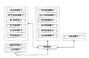
- FIG. 3 shows a main configuration of the optical display device manufacturing system according to the first embodiment.
- the manufacturing system of Embodiment 1 includes first and second pre-inspection peeling devices 13 and 23, and first and second release film laminating devices 15 and 25 in the configuration of the manufacturing system of Embodiment 2 to be described later. This is a configuration example that is not. Further, as another embodiment of the manufacturing system of the first embodiment, a configuration in which the first and second defect inspection devices 14 and 24 are not provided can be exemplified.
- the exclusion process by the 1st, 2nd exclusion apparatus 19 and 29 it is not limited to the case where the optical member (for example, polarizing plate with a surface protection film) determined as inferior goods is excluded,
- the optical member for example, polarizing plate with a surface protection film
- sampling of process inspection An example of the case of exclusion for sampling of quality inspection is also exemplified.
- optical display unit examples include a glass substrate unit of a liquid crystal cell and an organic EL light emitting unit.
- the optical member of the present invention may have a single-layer structure or a laminated structure in which a plurality of films are laminated.
- the member is exemplified.
- a transparent film for protection may be laminated
- an adhesive is formed on one surface of the optical member so as to be attached to the optical display unit, and a long release film is provided to protect the adhesive, and the optical member with the release film is provided.
- the optical member may have a surface protective film laminated on the outermost surface different from the surface on which the long release film is formed.
- the surface protective film and the optical member with a release film are referred to as sheet products.
- the optical member before being unrolled from the roll material and cut may be referred to as a long optical member.
- the optical member attached to the optical display unit W is referred to as a first optical member, and the optical member to be excluded without being attached to the optical display unit is referred to as a second optical member.
- Judgment of the object to be excluded may be based on a defect inspection result or may be based on an exclusion instruction by an operator. In the following, an example of determination based on a defect inspection result is shown.
- First roll original fabric preparation step (FIG. 1, S1).
- a long first sheet product (first laminated optical member) is prepared as a first roll.
- variety of a 1st roll original fabric is dependent on the bonding size to an optical display unit.
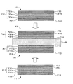
- the laminated structure of the first sheet product F1 includes an optical member F11, a first release film F12, and a surface protective film F13.
- the first optical member F11 includes a first polarizer F11a, a first film F11b having an adhesive layer (not shown) on one side thereof, and a second film having an adhesive layer (not shown) on the other side.
- the protective film may be comprised only in one surface at the optical member F11, and it can comprise so that the other direction may be protected with a release film through an adhesive layer.
- the first and second films F11b and F11c are, for example, polarizer protective films (for example, triacetyl cellulose film, PET film, etc.).
- the second film F11c is bonded to the optical display unit surface side via the first adhesive F14.
- a surface treatment can be applied to the first film F11b. Examples of the surface treatment include a hard coat treatment, an antireflection treatment, a treatment for the purpose of prevention of sticking, diffusion or antiglare, and the like.
- the first release film F12 is provided via the second film F11c and the first pressure-sensitive adhesive layer F14.
- the surface protection film F13 is provided through the 1st film F11b and the adhesive layer F15. Specific configurations of the first and second films F11b and F11c will be described later. Below, the laminated structure of a polarizer and a polarizer protective film may be called a polarizing plate.
- the following processes are performed in an isolated structure that is isolated in the factory, and the cleanliness is maintained. In particular, it is important that the cleanliness is maintained in the bonding step of bonding the optical member to the optical display unit.
- the first sheet product (first laminated optical member) F1 is fed out from the first roll stock prepared and installed, and is conveyed downstream.
- the first conveying device 12 that conveys the first sheet product F1 is configured by, for example, a nip roller pair, a tension roller, a rotation driving device, an accumulating device A, a sensor device, a control device, and the like.
- the defect inspection method includes a method of photographing and processing images with transmitted light and reflected light on both sides of the first sheet product F1, and an inspection polarizing film between the CCD camera and the inspection object.
- a method is mentioned. Note that a known method can be applied to the image processing algorithm, and for example, a defect can be detected by density determination by binarization processing.
- the defect information obtained by the first defect inspection apparatus 14 is linked together with the position information (for example, position coordinates), transmitted to the control apparatus 1, and contributes to a cutting method by the first cutting apparatus 16 described later. be able to.
- the first cutting device 16 leaves the first release film F12 (without cutting), and cuts the surface protective film F13, the pressure-sensitive adhesive layer F15, the optical member F11, and the first pressure-sensitive adhesive layer F14 into a predetermined size.
- the target optical member to be attached to the optical display unit W is the first optical member
- the optical member to be excluded is the second optical member.
- the cutting means include a laser device, a cutter, and other known cutting means. Based on the defect information obtained by the first defect inspection apparatus 14, the cutting is performed so as to avoid the defect. Thereby, the yield of an optical member improves significantly.
- the second optical member of the object to be excluded including the defect is excluded by a first rejecting device 19 described later, and is not attached to the optical display unit W.
- Non-defective product determination (FIG. 1, S5).
- the determination criteria for the non-defective product determination are set in advance, and are set according to, for example, the number of defects per predetermined area, the defect size, and the type of defect. Non-defective product judgment becomes more severe as the display performance with higher accuracy is required.
- First optical member bonding step (FIG. 1, S6-1). A bonding process of the optical member F11 (corresponding to the first optical member) determined to be non-defective by the defect inspection is performed.
- the first optical member F11 with the surface protective film F13 is bonded to the floor-side surface of the optical display unit W in a laid-down state. Thereby, the first optical member is bonded to one surface of the optical display unit W.
- the 1st optical member F11 from which the said 1st release film F12 was removed using the 1st bonding apparatus 18 is 1st. 1 It bonds to the optical display unit W through the adhesive layer F14. At the time of bonding, as will be described later, the first optical member F11 and the optical display unit W are sandwiched and pressed between a pressing roller 181 and a guide roller 182 that constitute a pair of bonding rollers.
- Second optical member removal step of the object to be excluded (FIG. 1, S6-2).
- the optical member F11 (corresponding to the second optical member) determined as a defective product by the defect inspection is excluded as an object to be excluded.
- a configuration example of the exclusion process will be described later.
- the cleaning step (FIG. 1, S7).
- the surface of the optical display unit W is cleaned by the polishing cleaning device 10 and the water cleaning device 11.
- the cleaned optical display unit W is transported to the first bonding apparatus 18 by the transport mechanism.
- the transport mechanism includes, for example, a transport roller, a transport direction switching mechanism, a rotation drive device, a sensor device, and a control device.
- first roll original fabric preparation step the first inspection step, the first cutting step, the first optical member bonding step, and the cleaning step are preferably performed on a continuous production line.
- the first optical member F11 is bonded to one surface of the optical display unit W.
- the manufacturing process which affixes an optical member on another surface similarly is demonstrated.
- an optical member attached to the optical display unit is referred to as a first optical member
- an optical member that is excluded without being attached to the optical display unit is referred to as a second optical member. Called.
- Second roll original fabric preparation step (FIG. 1, S11).
- a long second sheet product (second laminated optical member) F2 is prepared as a second roll.
- the second sheet product F2 includes an optical member F21, a second release film F22, and a surface protection film F23.
- the optical member F21 includes a second polarizer 21a, a third film F21b having an adhesive layer (not shown) on one side thereof, and a fourth film F21c having an adhesive layer (not shown) on the other side.
- the protective film may be comprised only in one surface at the optical member F21, and it can comprise so that the other direction may be protected with a release film through an adhesive layer.
- the third and fourth films F21b and F21c are, for example, polarizer protective films (for example, triacetyl cellulose film, PET film, etc.).
- the fourth film F21c is bonded to the optical display unit surface side via the second pressure-sensitive adhesive layer F24.
- the third film F21b can be subjected to a surface treatment. Examples of the surface treatment include a hard coat treatment, an antireflection treatment, a treatment for the purpose of prevention of sticking, diffusion or antiglare, and the like.
- the second release film F22 is provided via the fourth film F21c and the second pressure-sensitive adhesive layer F24.
- the surface protection film F23 is provided through the 3rd film F21b and the adhesive layer F25. Specific configurations of the third and fourth films F21b and F21c will be described later.
- the second sheet material F2 is fed out from the prepared and installed second roll, and is conveyed downstream.
- the second conveying device 22 that conveys the second sheet product F2 includes, for example, a nip roller pair, a tension roller, a rotation driving device, an accumulating device A, a sensor device, a control device, and the like.
- Second inspection step (FIG. 1, S13).
- the second sheet material F2 is inspected for defects using the second defect inspection device 24.
- the defect inspection method here is the same as the method using the first defect inspection apparatus described above.
- Second cutting step (FIG. 1, S14).
- the second cutting device 26 leaves the second release film F22 (without cutting), and cuts the surface protective film F23, the pressure-sensitive adhesive layer F25, the optical member F21, and the second pressure-sensitive adhesive layer F24 into a predetermined size.
- the target optical member to be attached to the optical display unit W is the first optical member
- the optical member to be excluded is the second optical member.
- the cutting means include a laser device, a cutter, and other known cutting means. Based on the information on the defect obtained by the second defect inspection apparatus 24, it is configured to cut so as to avoid the defect. Thereby, the yield of an optical member improves significantly.
- the optical member F ⁇ b> 21 that is an object to be excluded including defects is excluded by a second exclusion device 29 described later, and is not attached to the optical display unit W.
- Non-defective product determination (FIG. 1, S15). As a result of the defect inspection by the second defect inspection device 24, it is determined whether or not it is a non-defective product.
- the determination criteria for the non-defective product determination are set in advance, and are set according to, for example, the number of defects per predetermined area, the defect size, and the type of defect. Non-defective product judgment becomes more severe as the display performance with higher accuracy is required.
- First optical member bonding step (FIG. 1, S16-1). Bonding processing of the optical member F21 (corresponding to the first optical member) determined to be non-defective in the defect inspection is performed.
- the 1st optical member F21 with a surface protection film is affixed on the surface by the side of the ceiling of the optical display unit W1 in the state of lying down. Thereby, an optical member (with a surface protection film) is formed on both surfaces of the optical display unit W.
- the 1st optical member F21 from which the said 2nd release film F22 was removed using the 2nd bonding apparatus 28 is 1st. 2 It bonds together with the optical display unit W1 through the adhesive layer F24.
- the optical display unit W1 is rotated 90 degrees by the transport direction switching mechanism of the transport mechanism, and the polarizer of the first optical member F11 and the first optical member F21. In some cases, the polarizers have a crossed Nicols relationship.
- the first optical member F21 and the optical display unit W1 are sandwiched between a pair of pasting rollers (281, 282) to be pressure-bonded.
- the first optical member F11 is bonded to one surface of the optical display unit W
- the first optical member F21 is bonded to the other surface
- the optical display device W12 having the optical member (with a surface protective film) provided on both surfaces is manufactured. can do.
- Excluding step of removing the second optical member to be excluded (FIG. 1, S16-2).
- the optical member F21 (corresponding to the second optical member) determined as a defective product by the defect inspection is excluded as an object to be excluded.
- a configuration example of the exclusion process will be described later.
- the inspection device 30 inspects the optical display device W12 obtained by attaching the optical member to both surfaces of the optical display unit.
- the inspection method include a method of capturing an image and processing an image using reflected light on both surfaces of the optical display device W12.
- a method of installing a polarizing film for inspection between the CCD camera and the inspection object is also exemplified.
- the method of irradiating light from the one surface side of the optical display device W12, photographing the transmitted light image, analyzing the image, and detecting defects is exemplified. Note that a known method can be applied to the image processing algorithm, and for example, a defect can be detected by density determination by binarization processing.
- the non-defective product determination of the optical display device W12 is performed.
- the non-defective product determined optical display device W12 is transported to the next mounting process. If a defective product is determined, a rework process is performed, a new optical film is applied, and then inspected.If a good product is determined, the process proceeds to a mounting process. Discarded.
- the optical display device W12 can be suitably manufactured by executing the first optical member F11 bonding step and the first optical member F21 bonding step in a continuous production line.
- the optical member can be bonded to the optical display unit W in an environment in which cleanliness is ensured, and a high-quality optical display device W12 is manufactured. can do.
- defect information (defect coordinates, defect type, size, etc.) of the first and second sheet products is coded in a predetermined pitch unit (for example, 1000 mm). It may be attached as information (for example, QR code, barcode). In such a case, before the cutting, the code information is read and analyzed, and cut into a predetermined size in the first and second cutting steps so as to avoid the defective portion.
- the part including the defect is removed or bonded to a member that is not the optical display unit, and the non-defective sheet optical member cut to a predetermined size is bonded to the optical display unit.
- the yield of the optical member is significantly improved.
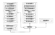
- FIG. 2 shows a flowchart of the manufacturing method of the optical display device according to the second embodiment.
- FIG. 4 shows a main configuration of the optical display device manufacturing system according to the second embodiment. A process similar to that of the first embodiment will be briefly described.
- First roll original fabric preparation step (FIG. 2, S1).
- a long first sheet product (first laminated optical member) F1 is prepared as a first roll original.
- the laminated structure of the first sheet product F1 is the same as that of the first embodiment shown in FIG.
- the first pre-inspection peeling device 13 peels the release film F12 from the conveyed first sheet product F1. Details of the peeling mechanism will be described later.
- the 1st fault inspection apparatus 14 test inspects the fault of the optical member with a surface protection film after a release film removal process. It is not necessary to consider the phase difference inherent in the release film F12 and the defects such as foreign matter or scratches attached to or inherent in the release film F12, and the optical member F11 can be inspected for defects.
- the method of defect inspection is as described above.
- the optical member F11 (corresponding to the second optical member), which is an object to be excluded including defects, is excluded by a first exclusion device 19 described later, and is not attached to the optical display unit W.
- the 1st release film bonding apparatus 15 bonds the release film H12 to the optical member F11 via the 1st adhesive layer F14 after a 1st fault test process. In order to maintain flatness, it is preferable to perform the bonding so that bubbles such as bubbles do not occur. The detail of the 1st release film bonding apparatus 15 is mentioned later.
- First cutting step (FIG. 2, S26).
- the first cutting device 16 does not cut the release film H12, and the surface protective film F13, the pressure-sensitive adhesive layer F15, the optical member F11, and the first pressure-sensitive adhesive layer F14 have a predetermined size.
- Disconnect examples include a laser device, a cutter, and other known cutting means.
- Non-defective product determination (FIG. 2, S27). As a result of the defect inspection by the first defect inspection apparatus 14, it is determined whether or not the product is a non-defective product.
- the determination criteria for the non-defective product determination are set in advance, and are set according to, for example, the number of defects per predetermined area, the defect size, and the type of defect. Non-defective product judgment becomes more severe as the display performance with higher accuracy is required.
- the 1st optical member F11 from which the said 1st release film F12 was removed using the 1st bonding apparatus 18 is 1st. 1 It is bonded to the optical display unit W through the adhesive layer F14. At the time of pasting, as will be described later, the first optical member F11 and the optical display unit W are sandwiched between a pair of pasting rollers (pressing roller 181 and guide roller 182) to be pressure-bonded.
- Second optical member exclusion step of the object to be excluded (FIG. 2, S28-2). Exclusion processing is performed on the optical member F11 (corresponding to the second optical member), which is an object to be excluded, which has been determined to be defective in the defect inspection. A configuration example of the exclusion process will be described later.
- Second roll original fabric preparation step (FIG. 2, S11).
- a long second sheet product (second laminated optical member) F2 is prepared as a second roll.
- the laminated structure of the second sheet product F2 has the configuration shown in FIG.
- Transfer process (FIG. 2, S12).
- the second sheet material F2 is fed out from the prepared and installed second roll, and is conveyed downstream.
- the second pre-inspection peeling device 23 peels the release film F22 from the second sheet product F2 being conveyed. Details of the peeling mechanism will be described later.
- Second defect inspection step (FIG. 2, S34).
- the method of defect inspection is as described above.
- the optical member F21 including the defect (corresponding to the second optical member) is excluded by a second exclusion device 29 described later, and is configured not to be attached to the optical display unit.
- the 2nd release film bonding apparatus 25 bonds the release film H22 to the optical member F21 through the 2nd adhesive layer F24 after a 2nd fault test process. In order to maintain flatness, it is preferable to perform the bonding so that bubbles such as bubbles do not occur. The detail of the 2nd release film bonding apparatus 25 is mentioned later.
- Second cutting step (FIG. 2, S36).
- the second cutting device 26 does not cut the release film H22, and the surface protective film F23, the pressure-sensitive adhesive layer F25, the optical member F21, and the second pressure-sensitive adhesive layer F24 have a predetermined size.
- Disconnect examples include a laser device, a cutter, and other known cutting means.
- Non-defective product determination (FIG. 2, S37). As a result of the defect inspection by the second defect inspection device 24, it is determined whether or not it is a non-defective product.
- the determination criteria for the non-defective product determination are set in advance, and are set according to, for example, the number of defects per predetermined area, defect size, and defect type. Non-defective product judgment becomes more severe as the display performance with higher accuracy is required.
- First optical member bonding step (FIG. 2, S38-1). Bonding processing of the optical member F21 (corresponding to the first optical member) determined to be non-defective in the defect inspection is performed. The first optical member F21 with the surface protective film is bonded to the ceiling side surface of the optical display unit in a laid-down state.
- the first optical member F21 (surface) from which the second release film F22 has been removed using the second bonding device 28 A protective film is attached) to the optical display unit W1 through the second pressure-sensitive adhesive layer F24.
- the optical display unit W1 is rotated 90 degree
- the F21 polarizer may be in a crossed Nicols relationship.
- the first optical member F21 and the optical display unit W1 are sandwiched between a pair of pasting rollers (281, 282) to be pressure-bonded.
- a pair of pasting rollers (281, 282)
- Second optical member exclusion step of the object to be excluded (FIG. 2, S38-2). Exclusion processing of the optical member F21 (corresponding to the second optical member) determined as defective by the defect inspection is performed. A configuration example of the exclusion process will be described later.
- the non-defective product of the optical display device W12 is determined.
- the non-defective product determined optical display device W12 is transported to the next mounting process. If a defective product is determined, a rework process is performed, a new optical member is applied, and then inspected. If a non-defective product is determined, the process proceeds to a mounting process. Discarded.
- the optical display device can be preferably manufactured by executing the bonding process of the first optical member F11 and the first optical member F21 bonding process on a continuous production line.
- the optical member can be bonded to the optical display unit in an environment in which cleanliness is ensured, and a high-quality optical display device is manufactured. Can do.
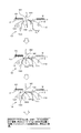
- FIG. 5 is a diagram showing the first peeling device 17, the first sticking device 18, and the first exclusion device 19.
- FIG. 6 is a view showing the second peeling device 27, the second sticking device 28, and the second exclusion device 29.
- FIG. 7 is a diagram for explaining the configuration of the first exclusion device 19 and the exclusion operation.
- the structure of the 1st exclusion apparatus 19 is not restrict
- the second exclusion device 29 has the same configuration as that of the first exclusion device 19, but the exclusion operation is different, and the exclusion operation will be described with reference to FIG. 8.
- the first roll raw material of the long first sheet product (first laminated optical member) F1 is installed on a roller mount device that is linked to a motor or the like so as to rotate freely or at a constant rotational speed.
- the rotation speed is set by the control device 1 and the drive is controlled.
- the first transport device 12 is a transport mechanism that transports the first sheet product F1 to the downstream side.
- the first transport device 12 is controlled by the control device 1.
- the first pre-inspection peeling device 13 is configured to peel the release film from the conveyed first sheet product F1 and to wind the release film on a winding device.
- the winding speed of the winding device is controlled by the control device 1.
- As a peeling mechanism for peeling the release film it has a knife edge part with a sharp tip, and the release film is wound around this knife edge part and transferred in reverse, thereby releasing the release film and releasing the mold. It is comprised so that the 1st sheet product F1 after peeling a film may be conveyed in a conveyance direction.
- the first defect inspection device 14 performs defect inspection after the release film is peeled off.
- the first defect inspection device 14 detects the defect by analyzing the image data captured by the CCD camera, and further calculates its position coordinates. The position coordinates of this defect are provided for the skip cut by the first cutting device 16 described later.
- the 1st release film bonding apparatus 15 bonds the release film H12 to the optical member F11 through the 1st adhesive layer F14 after a 1st fault test
- the release film H12 is unwound from the roll of the release film H12, and the release film H12 and the optical member F11 are sandwiched by one or a plurality of roller pairs, and are bonded together by applying a predetermined pressure with the roller pairs.
- the rotation speed, pressure control, and conveyance control of the roller pair are controlled by the control device 1.
- the 1st cutting device 16 does not cut
- the first cutting device 16 is, for example, a laser device. Based on the position coordinates of the defect detected in the first defect inspection process, the first cutting device 16 cuts to a predetermined size so as to avoid the defect portion. That is, the cut product including the defective portion is rejected as a defective product by the first rejecting device 19 in a subsequent process. Alternatively, the first cutting device 16 may continuously cut into a predetermined size while ignoring the existence of the defect. In this case, it can be configured to remove the portion without bonding in a bonding process described later. Control in this case also depends on the function of the control device 1.
- the first cutting device 16 is provided with a holding table that sucks and holds the first sheet product F1 from the ceiling surface side, and a laser device is provided below the floor side of the first sheet product F1.
- the first sheet product F1 is moved in parallel so that the laser is scanned in the width direction, and the first optical member F11, the first pressure-sensitive adhesive layer F14, the surface protective film F13, and the pressure-sensitive adhesive layer, leaving the uppermost release film H12.
- F15 is cut at a predetermined pitch in the conveying direction (hereinafter referred to as “half cut” as appropriate).
- the accumulation device of the transport mechanism is moved in the vertical direction so as not to stop the continuous transport of the downstream and upstream first sheet products F1. It is configured. This operation is also controlled by the control device 1.
- the 1st bonding apparatus 18 is optical display unit through the 1st adhesive layer F14 for the optical member F11 (with surface protection film) from which the release film H12 was peeled by the 1st peeling apparatus 17 after the said cutting process. Affix to W. Only the optical member F11 (corresponding to the first optical member) determined to be non-defective by the first inspection device 14 is bonded to the optical display unit W. The optical member F11 and the optical display unit W determined to be non-defective are conveyed in synchronization with the bonding position. As shown in FIG. 5, the optical member F ⁇ b> 11 and the optical display unit W are conveyed so as to overlap each other. This is realized by controlling the control device 1 so that the first transport device 12 (including the accumulation device) and the transport mechanism are interlocked.
- the optical member F11 is bonded to the surface of the optical display unit W by the pressing roller 181 and the guide roller 182.
- the control device 1 controls the pressing pressure and driving operation of the pressing roller 181 and the guide roller 182.
- the peeling mechanism 171 of the first peeling device 17 has a knife edge portion with a sharp tip, and the release film H12 is wrapped around the knife edge portion and transferred in reverse, thereby peeling the release film H12.
- the optical member F11 (with a surface protection film) after peeling off the release film H12 is configured to be sent out to the optical display unit W surface.
- the peeled release mold H12 is wound around a roll 172.
- the winding control of the roll 172 is controlled by the control device 1.
- the laminating mechanism is composed of a pressing roller 181 and a guide roller 182 disposed opposite thereto.
- the guide roller 182 is composed of a rubber roller that is rotationally driven by a motor, and is provided with a drive mechanism that can move the roller up and down.
- a pressing roller 181 made of a metal roller that is rotationally driven by a motor is provided immediately above the driving roller 181 with a drive mechanism that can move the roller up and down.
- the pressing roller 181 moves away from the bonding position so as to open a roller interval.
- both the guide roller 182 and the pressing roller 181 may be rubber rollers or metal rollers.
- the optical display unit W is cleaned by various cleaning devices and is transported by the transport mechanism.
- the transport control of this transport mechanism is also controlled by the control device 1.
- the 1st exclusion apparatus 19 which excludes the optical member (equivalent to a 2nd optical member) of the exclusion target object 200 is demonstrated.
- the operation of the first exclusion device 19 will be described with reference to FIG.
- the first exclusion device 19 is disposed on the floor side with respect to the optical display unit W.
- the exclusion roller 192 is moved to the exclusion position by a drive mechanism (not shown).
- a known drive mechanism can be used as the drive mechanism for driving the exclusion roller.
- An exclusion film 191 (corresponding to a tape member) is stretched over the exclusion roller 192.
- the exclusion film 191 is drawn out from the winding means of the exclusion film 191 and wound around the take-up roller 193 via the exclusion roller 192.
- an adhesive tape can be used instead of the exclusion film 191.
- the release film H12 is peeled from the second optical member (with the surface protective film) by the knife edge 171 of the first peeling device 17, and the second optical member is directed in the floor direction from the bonding position of the optical display unit W. Dodge. Then, the exclusion object 200 (second optical member with a surface protective film) is sandwiched between the pressing roller 181 and the exclusion roller 192, and the exclusion object 200 is attached to the exclusion film 191 using the first adhesive layer F14. The exclusion object 200 is excluded by winding up the exclusion film 191 with a winding roller 193 (corresponding to a winding means).
- the tip position of the knife edge 171 is rotated by the rotating means from the bonding position direction, and the tip position rotates to the floor surface side, so that the object 200 to be removed is moved from the bonding position of the optical display unit W to the floor direction. It is going.
- the transport of the optical display unit W is stopped (the transport mechanism includes an accumulation mechanism). ). Then, the pressing roller 181 moves downward to the exclusion position of the exclusion object 200.
- the knife edge 171 rotates, and the tip direction thereof is directed obliquely from the upper side to the floor side. This rotation angle is set according to the specification of the first sheet product F1, the conveyance speed, and the like.
- the exclusion roller 192 around which the exclusion film 191 is stretched moves to the position of the pressing roller 181.
- the release film H12 is peeled off by the knife edge 171, and the pressing target 181 and the exclusion roller 181 are attached so that the exclusion object 200 sent out at the same time is attached to the exclusion film 191 by the first adhesive layer F14. And 192.
- the exclusion object 200 is pressed against the exclusion roller 192 side by the pressing roller 181 and the exclusion object 200 is attached to the exclusion film 191 by the first adhesive layer F14. Then, the exclusion object 200 is wound around the winding roller 193 together with the exclusion film 191.
- the moving speed of the exclusion film 191 by the take-up roller 193 and the conveying speed of the exclusion object 200 are synchronized.
- a servo motor can be used for rotational driving of the take-up roller 193 and the conveyance roller (not shown) of the object 200 to be excluded, and the control device 1 can perform synchronous control by rotating each servo motor simultaneously at the same speed. . (6) After the exclusion object 200 is removed, the pressing roller 181, the exclusion roller 192, and the knife edge 171 return to the original positions. The above operation is controlled by the control device 1.
- FIG. (1) movement of the 2nd exclusion apparatus 29 is demonstrated using FIG. (1)
- the optical member F21 corresponding to the second optical member
- the conveyance of the optical display unit W1 is stopped.
- the conveyance by the long release film F23 is also stopped once.
- the accumulating mechanism is provided in the transport mechanism.
- the guide roller 282 moves vertically downward.
- the exclusion roller 292 on which the exclusion film 291 is stretched is moved to a bonding position, which is a fixed position of the guide roller 282, by the driving mechanism (movement process).
- the pressing roller 281 moves vertically downward.
- the pressing roller 281 presses the exclusion target object 200 against the exclusion roller 292 side, and attaches the front portion of the exclusion target object 200 to the non-viscous surface of the exclusion film 291 via the second adhesive layer F24 ( Adhesion treatment).
- Adhesion treatment Adhesion treatment
- the conveyance by the long release film F22 is resumed, and the winding by the winding roller 293 is started, and the exclusion object 200 is wound around the winding roller 293 (winding device) together with the exclusion film 291. Taken (winding process).
- the take-up moving speed of the exclusion film 291 by the take-up roller 293 is synchronized with the delivery speed of the exclusion object 200.
- a servo motor can be used for rotational driving of the take-up roller 293 and the conveying roller (not shown) of the object 200 to be excluded, and the control device 1 can perform synchronous control by rotating each servo motor simultaneously at the same speed.
- the exclusion film 291 to which the second optical member F21 is attached is wound up to a position where the entire second optical member F21 does not overlap, and then the winding stops.
- the pressing roller 281 moves up, the removal roller 292 returns to the original position, and the guide roller 282 returns to the original position.
- the above operation is controlled by the control device 1.
- the optical display unit W1 to which the first optical member F11 is attached is conveyed downstream, and the optical member F21 of the second sheet product (second laminated optical member) F2 is attached thereto.
- the description of the same device configuration will be briefly described.
- the optical display unit W1 is rotated 90 ° by the transport direction switching mechanism of the transport mechanism.
- the optical member F21 is bonded.
- each step is processed with the second sheet product F2 inverted (with the release film on the top surface), and the optical member F21 is replaced with the optical display unit. It is comprised so that it may stick together from the lower side of W1.
- the second roll raw material of the long second sheet product F2 is installed on a roller mount device that is linked to a motor or the like so as to rotate freely or at a constant rotational speed.
- the rotation speed is set by the control device 1 and the drive is controlled.
- the second transport device 22 is a transport mechanism that transports the second sheet product F2 to the downstream side.
- the second transport device 22 is controlled by the control device 1.
- the second pre-inspection peeling device 23 has a configuration in which the release film is peeled from the conveyed second sheet product F2 and wound on a winding device.
- the winding speed of the winding device is controlled by the control device 1.
- the tip has a sharp knife edge part, and a release film is wound around the knife edge part and reversed and transferred to peel off the release film and peel off the release film.
- the second sheet product F2 is configured to be conveyed in the conveyance direction.
- the second defect inspection device 24 performs defect inspection after the release film is peeled off.
- the second defect inspection device 24 analyzes the image data picked up by the CCD camera, detects the defect, and calculates its position coordinates. The position coordinates of this defect are provided for the skip cut by the second cutting device 26 described later.
- the second release film bonding apparatus 25 bonds the release film H22 to the optical member F21 via the second pressure-sensitive adhesive layer F24 after the second defect inspection.
- the release film H22 is unwound from the roll of the release film H22, and the release film H22 and the optical member F21 are sandwiched by one or a plurality of roller pairs, and are bonded together by applying a predetermined pressure with the roller pairs.
- the rotation speed, pressure control, and conveyance control of the roller pair are controlled by the control device 1.
- the second cutting device 26 leaves the release film H22 (without cutting), the optical member F21, the surface protective film F23, the second pressure-sensitive adhesive layer F24, and the pressure-sensitive adhesive.
- the layer F25 is cut into a predetermined size.
- the second cutting device 26 is, for example, a laser device. Based on the position coordinates of the defect detected in the second defect inspection process, the second cutting device 26 cuts to a predetermined size so as to avoid the defect portion. That is, the cut product including the defective portion is rejected as a defective product by the second rejection device 29 in a later process. Or the 2nd cutting device 26 may ignore the presence of a fault, and may cut continuously to a predetermined size. In this case, it can be configured such that the portion is removed without being bonded in the bonding process described later. Control in this case also depends on the function of the control device 1.
- the second cutting device 26 is provided with a holding table for sucking and holding the second sheet product F2 from the floor side, and a laser device is provided on the ceiling side of the second sheet product F2.
- the second sheet product F2 is moved in parallel so as to scan the laser in the width direction, and the optical member F21, the second pressure-sensitive adhesive layer F24, the surface protective film F23, and the pressure-sensitive adhesive layer F25 are left leaving the lowermost release film H22. Cut at a predetermined pitch in the conveying direction.
- the accumulation device of the transport mechanism is moved in the vertical direction so as not to stop the continuous transport of the downstream and upstream second sheet products F2. It is configured. This operation is also controlled by the control device 1.
- the 2nd bonding apparatus 28 is optical display unit W1 through the 2nd adhesive layer F24 for the optical member F21 (with surface protection film) by which the release film H22 was peeled by the 2nd peeling apparatus 27 after the cutting process.
- the optical member F ⁇ b> 21 is bonded to the surface of the optical display unit W ⁇ b> 1 by the pressing roller 281 and the guide roller 282 while being bonded.
- the control device 1 controls the pressing pressure and driving operation of the pressing roller 281 and the guide roller 282. Only the optical member F21 (corresponding to the first optical member) determined to be non-defective by the second inspection device 24 is bonded to the optical display unit W1.
- the optical member F21 determined to be non-defective and the optical display unit W1 are conveyed in synchronization with the bonding position. As shown in FIG. 6, it is conveyed so that each front-end
- the peeling mechanism 271 of the second peeling device 27 has a knife edge portion with a sharp tip, and the release film H22 is wound around the knife edge portion and reversely transferred to peel the release film H22.
- the first optical member F21 after peeling off the release film H22 is configured to be sent out to the surface of the optical display unit W1.
- the peeled release film H22 is wound up on a roll 272.
- the winding control of the roll 272 is controlled by the control device 1.
- the laminating mechanism is composed of a pressing roller 281 and a guide roller 282 arranged opposite to it.
- the guide roller 282 is composed of a rubber roller that is rotationally driven by a motor, and is arranged to be movable up and down.
- a pressing roller 281 made of a metal roller that is rotationally driven by a motor is disposed directly below it.
- the pressing roller 281 is moved to a lower position so as to open a roller interval.
- both the guide roller 282 and the pressing roller 281 may be rubber rollers or metal rollers.
- the optical display device W12 obtained by bonding the optical members F11 and F21 to the optical display unit W is transported to the inspection device 30.
- the inspection device 30 performs an inspection on both sides of the optical display device W12 that has been conveyed.
- the light source of the inspection device 30 irradiates vertically from the lower surface side of the optical display device W12, and the transmitted light image is captured as image data by the CCD camera of the inspection device 30.
- the surface of the optical display device W12 can be irradiated with a light source at a predetermined angle, and the reflected light image can be captured as image data by a CCD camera. Defects are image-processed and analyzed from these image data, and non-defective products are determined.
- the operation timing of each apparatus is calculated by, for example, a method of detecting by arranging a sensor at a predetermined position, or by detecting a rotary member of the transfer apparatus or the transfer mechanism with a rotary encoder or the like.
- the control device 1 may be realized by a cooperative action of a software program and hardware resources such as a CPU and a memory. In this case, a memory is stored in advance for the program software, processing procedure, various settings, and the like. Further, it can be configured by a dedicated circuit or firmware.
- the control apparatus 1 is the structure which controls each apparatus collectively, it is not restricted to this, A control part is provided for each apparatus, and according to the command from the control apparatus 1, each apparatus is provided.
- the control unit can also be configured to control the operation of each device.
- the optical member F11 (with the surface protective film) is attached from the lower surface of the optical display unit W
- the optical member F21 (with the surface protective film) is attached from the upper surface of the optical display unit W1.
- the first and second exclusion devices 19 and 29 are located below the transport path of the optical display units W and W1. Thereby, collection
- the optical display unit is laid on its side, and the optical member is attached from the floor side surface. Can be configured to attach.
- each treatment of dyeing, crosslinking and stretching of the polyvinyl alcohol film need not be performed separately and may be performed simultaneously, and the order of the treatments may be arbitrary.
- a polyvinyl alcohol film is immersed in a solution containing iodine or a dichroic dye, dyed by adsorbing iodine or a dichroic dye, washed, and stretched in a solution containing boric acid or borax. After uniaxial stretching at a magnification of 3 to 7 times, it is dried.
- the adhesive treatment between the polarizer and the transparent polarizer protective film that is the protective layer is not particularly limited, but for example, an adhesive made of a vinyl alcohol polymer, boric acid, borax, or glutaraldehyde Or an adhesive comprising at least a water-soluble crosslinking agent of a vinyl alcohol polymer such as melamine or oxalic acid.
- an adhesive layer is formed as a coating / drying layer or the like of an aqueous solution.
- other additives and a catalyst such as an acid can be blended as necessary.
- Polarizer protective layer Polarizer protective film
- An appropriate transparent film can be used for the polarizer protective layer provided on one side or both sides of the polarizer.
- a thermoplastic resin excellent in transparency, mechanical strength, thermal stability, moisture barrier property, isotropy, etc. is used.
- thermoplastic resins include cellulose resins such as triacetyl cellulose, polyester resins, polyethersulfone resins, polysulfone resins, polycarbonate resins, polyamide resins, polyimide resins, polyolefin resins, (meth) acrylic resins, cyclic Examples thereof include polyolefin resins (norbornene resins), polyarylate resins, polystyrene resins, polyvinyl alcohol resins, and mixtures thereof.
- a transparent protective film is bonded to one side of the polarizer by an adhesive layer.
- thermosetting resin such as a system or an ultraviolet curable resin
- a thermosetting resin such as a system or an ultraviolet curable resin
- the additive include an ultraviolet absorber, an antioxidant, a lubricant, a plasticizer, a release agent, a coloring inhibitor, a flame retardant, a nucleating agent, an antistatic agent, a pigment, and a coloring agent.
- the transparent protective film may be subjected to surface modification treatment in order to improve adhesiveness with a polarizer before applying an adhesive.
- Specific examples of the treatment include corona treatment, plasma treatment, flame treatment, ozone treatment, primer treatment, glow treatment, saponification treatment, and treatment with a coupling agent.
- an antistatic layer can be appropriately formed.
- the optical member according to the present invention can be exemplified by an optical film having a laminated structure in which various optical layers are laminated in practical use.
- the optical layer is not particularly limited, for example, on the surface of the transparent protective film that does not adhere the polarizer (the surface on which the adhesive coating layer is not provided), hard coat treatment or antireflection treatment, Examples thereof include a method of applying a surface treatment for the purpose of preventing sticking, diffusion or antiglare, and laminating an alignment liquid crystal layer for the purpose of viewing angle compensation or the like.
- one or two optical films are used for forming a liquid crystal display device such as a reflection plate, a semi-transmission plate, a retardation plate (including a wave plate ( ⁇ plate) such as 1/2 or 1/4). The pasted ones are also included.
- An example of the optical film laminated on the polarizer is a retardation plate.
- the retardation plate include a birefringent film obtained by uniaxially or biaxially stretching a polymer material, a liquid crystal polymer alignment film, and a liquid crystal polymer alignment layer supported by a film.
- the stretching treatment can be performed by, for example, a roll stretching method, a long gap stretching method, a tenter stretching method, a tubular stretching method, or the like.
- the stretching ratio is generally about 1.1 to 3 times in the case of uniaxial stretching.
- the thickness of the retardation plate is not particularly limited, but is generally 10 to 200 ⁇ m, preferably 20 to 100 ⁇ m.
- polymer material examples include polyvinyl alcohol, polyvinyl butyral, polymethyl vinyl ether, polyhydroxyethyl acrylate, hydroxyethyl cellulose, hydroxypropyl cellulose, methyl cellulose, polycarbonate, polyarylate, polysulfone, polyethylene terephthalate, polyethylene naphthalate, and polyethersulfone.
- the retardation plate may have an appropriate retardation according to the purpose of use, such as those for the purpose of compensating for various wavelength plates or birefringence of the liquid crystal layer, viewing angle, and the like. What laminated
- the polarizing plate according to the present invention and the laminated optical film member are provided with an adhesive layer for adhering to other members such as a liquid crystal cell.
- the pressure-sensitive adhesive layer is not particularly limited, but can be formed with a suitable pressure-sensitive adhesive according to the conventional type such as acrylic. Low moisture absorption and heat resistance due to prevention of foaming and peeling phenomenon due to moisture absorption, deterioration of optical characteristics due to thermal expansion difference, prevention of liquid crystal cell warpage, and formation of a high-quality and durable image display device. It is preferable that it is an adhesive layer excellent in property. Moreover, it can be set as the adhesion layer etc. which contain microparticles
- the adhesive layer may be provided on a necessary surface as necessary.
- a polarizing plate comprising a polarizer and a polarizer protective layer
- the adhesive layer is adhered to one or both surfaces of the polarizer protective layer as necessary.
- a layer may be provided.
- a release film (Release film)
- the exposed surface of the adhesive layer is temporarily covered with a release film (sometimes referred to as a separator) for the purpose of preventing contamination until it is put to practical use. Thereby, it can prevent contacting an adhesion layer in the usual handling state.
- a suitable thin leaf body such as a plastic film, rubber sheet, paper, cloth, non-woven fabric, net, foam sheet, metal foil, laminate thereof, and the like, silicone type or Appropriate conventional ones such as those coated with an appropriate release agent such as long-chain alkyl, fluorine-based, or molybdenum sulfide can be used.
- a surface protective film is formed on the polarizing plate opposite to the surface provided with the separator via a weak adhesive. Its main purpose is to prevent scratches and pollution.
- the surface protective film for example, plastic film, rubber sheet, paper, cloth, non-woven fabric, net, foamed sheet or metal foil, appropriate thin leaves such as laminates thereof, if necessary silicone type or long chain alkyl type, Appropriate ones according to the prior art such as those coated with an appropriate release agent such as fluorine-based or molybdenum sulfide can be used.
- the optical member of the present invention can be preferably used for forming various optical display devices such as liquid crystal display devices.
- the liquid crystal display device can be formed according to the conventional method. That is, a liquid crystal display device is generally formed by appropriately assembling components such as a liquid crystal cell (corresponding to an optical display unit), an optical film, and an illumination system as necessary, and incorporating a drive circuit. In the present invention, there is no particular limitation except that the optical film according to the present invention is used.
- the liquid crystal cell any type such as a TN type, an STN type, or a ⁇ type can be used.
Landscapes
- Physics & Mathematics (AREA)
- Nonlinear Science (AREA)
- Optics & Photonics (AREA)
- Crystallography & Structural Chemistry (AREA)
- Chemical & Material Sciences (AREA)
- General Physics & Mathematics (AREA)
- Mathematical Physics (AREA)
- Engineering & Computer Science (AREA)
- Manufacturing & Machinery (AREA)
- Mechanical Engineering (AREA)
- Liquid Crystal (AREA)
- Devices For Indicating Variable Information By Combining Individual Elements (AREA)
- Polarising Elements (AREA)
Priority Applications (4)
| Application Number | Priority Date | Filing Date | Title |
|---|---|---|---|
| US12/865,284 US8057619B2 (en) | 2008-04-08 | 2009-04-07 | Manufacturing system for an optical display device, manufacturing method for an optical display device, excluding device and excluding method |
| CN2009801012412A CN101884060B (zh) | 2008-04-08 | 2009-04-07 | 光学显示装置的制造系统、光学显示装置的制造方法、排除装置及排除方法 |
| PL09731115T PL2246835T3 (pl) | 2008-04-08 | 2009-04-07 | System do wytwarzania optycznego urządzenia wyświetlającego, sposób wytwarzania optycznego urządzenia wyświetlającego, oraz urządzenie usuwające i sposób usuwania |
| EP09731115.3A EP2246835B1 (de) | 2008-04-08 | 2009-04-07 | System zur herstellung einer optischen anzeigevorrichtung, verfahren zur herstellung einer optischen anzeigevorrichtung sowie entfernungsvorrichtung und entfernungsverfahren dafür |
Applications Claiming Priority (4)
| Application Number | Priority Date | Filing Date | Title |
|---|---|---|---|
| JP2008-100622 | 2008-04-08 | ||
| JP2008100622 | 2008-04-08 | ||
| JP2009092652A JP4551477B2 (ja) | 2008-04-08 | 2009-04-07 | 光学表示装置の製造システム、光学表示装置の製造方法、排除装置および排除方法 |
| JP2009-092652 | 2009-04-07 |
Publications (1)
| Publication Number | Publication Date |
|---|---|
| WO2009125771A1 true WO2009125771A1 (ja) | 2009-10-15 |
Family
ID=41161903
Family Applications (1)
| Application Number | Title | Priority Date | Filing Date |
|---|---|---|---|
| PCT/JP2009/057140 WO2009125771A1 (ja) | 2008-04-08 | 2009-04-07 | 光学表示装置の製造システム、光学表示装置の製造方法、排除装置および排除方法 |
Country Status (8)
| Country | Link |
|---|---|
| US (1) | US8057619B2 (de) |
| EP (1) | EP2246835B1 (de) |
| JP (1) | JP4551477B2 (de) |
| KR (1) | KR101008418B1 (de) |
| CN (1) | CN101884060B (de) |
| PL (1) | PL2246835T3 (de) |
| TW (1) | TW201007251A (de) |
| WO (1) | WO2009125771A1 (de) |
Cited By (5)
| Publication number | Priority date | Publication date | Assignee | Title |
|---|---|---|---|---|
| CN102298232A (zh) * | 2010-06-24 | 2011-12-28 | 日东电工株式会社 | 液晶显示面板的连续制造系统以及连续制造方法 |
| JP4844857B1 (ja) * | 2011-02-23 | 2011-12-28 | 住友化学株式会社 | 回収装置、貼合システム及び回収方法 |
| WO2012029716A1 (ja) * | 2010-09-02 | 2012-03-08 | 日東電工株式会社 | 連続ロール、並びに、液晶表示素子の製造方法及び製造システム |
| KR101169902B1 (ko) | 2011-02-23 | 2012-07-31 | 수미토모 케미칼 컴퍼니 리미티드 | 회수 장치, 접합 시스템 및 회수 방법 |
| WO2012147793A1 (ja) * | 2011-04-28 | 2012-11-01 | 住友化学株式会社 | ナイフエッジおよびこれを含む液晶表示装置の製造システム |
Families Citing this family (11)
| Publication number | Priority date | Publication date | Assignee | Title |
|---|---|---|---|---|
| WO2011105273A1 (ja) * | 2010-02-24 | 2011-09-01 | 住友化学株式会社 | 液晶表示装置の製造方法 |
| JP5181011B2 (ja) * | 2010-10-21 | 2013-04-10 | 日東電工株式会社 | 液晶表示素子の連続製造システムおよび液晶表示素子の連続製造方法 |
| JP5140788B2 (ja) | 2010-11-22 | 2013-02-13 | 日東電工株式会社 | 液晶表示素子の連続製造システムおよび液晶表示素子の連続製造方法 |
| JP4750227B1 (ja) | 2011-01-14 | 2011-08-17 | 日東電工株式会社 | 液晶表示素子の連続製造システムおよび液晶表示素子の連続製造方法 |
| JP5068876B1 (ja) | 2011-06-10 | 2012-11-07 | 日東電工株式会社 | 液晶表示素子の連続製造方法及び装置 |
| KR101860597B1 (ko) * | 2011-06-29 | 2018-05-23 | 수미토모 케미칼 컴퍼니 리미티드 | 나이프 엣지 및 이것을 포함하는 액정 표시 장치의 제조 시스템 |
| KR101318179B1 (ko) * | 2012-03-30 | 2013-10-16 | 주식회사 에스에프에이 | 릴투패널 편광필름 부착 장치 및 그 방법 |
| JP5307947B1 (ja) | 2012-03-30 | 2013-10-02 | 日東電工株式会社 | 液晶表示装置の製造方法 |
| KR101932562B1 (ko) * | 2012-09-18 | 2018-12-28 | 삼성디스플레이 주식회사 | 필름 부착장치 및 그것을 이용한 필름 부착방법 |
| JP5724147B2 (ja) | 2013-02-27 | 2015-05-27 | 住友化学株式会社 | 光学表示デバイスの生産システム |
| KR102360735B1 (ko) * | 2016-08-10 | 2022-02-08 | 에이지씨 엔지니아링 가부시키가이샤 | 기재 시트의 처리 방법, 개질 기재 시트의 제조 방법, 그래프트 중합 사슬이 형성된 기재, 및 이온 교환막 |
Citations (3)
| Publication number | Priority date | Publication date | Assignee | Title |
|---|---|---|---|---|
| JPS5752017A (en) | 1980-08-08 | 1982-03-27 | Sharp Corp | Tacky-polarizing-plate defective removing device automatic tacky-polarizing-plate sticking machine |
| JPH11333929A (ja) * | 1998-05-22 | 1999-12-07 | Somar Corp | フィルム張付装置における原反フィルムの連続的供給方法及び装置 |
| JP2007140046A (ja) * | 2005-11-17 | 2007-06-07 | Nitto Denko Corp | 光学表示装置の製造システム及びその製造方法 |
Family Cites Families (6)
| Publication number | Priority date | Publication date | Assignee | Title |
|---|---|---|---|---|
| KR100400399B1 (ko) * | 2001-11-23 | 2003-10-01 | 주식회사 엘지이아이 | 무전극 조명기기의 전등장치 |
| US7202923B2 (en) | 2001-11-27 | 2007-04-10 | Sharp Kabushiki Kaisha | Liquid crystal display with polarizer with inclined edge portion |
| CN1297844C (zh) | 2001-11-27 | 2007-01-31 | 夏普株式会社 | 液晶板、液晶板制造方法、液晶板制造设备和偏振片粘结设备 |
| CN1721935A (zh) * | 2004-07-13 | 2006-01-18 | 鸿富锦精密工业(深圳)有限公司 | 撕膜装置、偏光片贴附装置及撕膜方法 |
| PL2093041T3 (pl) | 2006-10-17 | 2013-08-30 | Nitto Denko Corp | Sposób przyklejania elementu optycznego i urządzenie wykorzystujące ten sposób |
| JP4724742B2 (ja) | 2008-01-09 | 2011-07-13 | 日東電工株式会社 | 光学表示装置の製造システムおよび光学表示装置の製造方法 |
-
2009
- 2009-04-07 PL PL09731115T patent/PL2246835T3/pl unknown
- 2009-04-07 KR KR1020107007623A patent/KR101008418B1/ko active IP Right Grant
- 2009-04-07 WO PCT/JP2009/057140 patent/WO2009125771A1/ja active Application Filing
- 2009-04-07 JP JP2009092652A patent/JP4551477B2/ja active Active
- 2009-04-07 US US12/865,284 patent/US8057619B2/en active Active
- 2009-04-07 EP EP09731115.3A patent/EP2246835B1/de active Active
- 2009-04-07 CN CN2009801012412A patent/CN101884060B/zh active Active
- 2009-04-08 TW TW098111713A patent/TW201007251A/zh unknown
Patent Citations (3)
| Publication number | Priority date | Publication date | Assignee | Title |
|---|---|---|---|---|
| JPS5752017A (en) | 1980-08-08 | 1982-03-27 | Sharp Corp | Tacky-polarizing-plate defective removing device automatic tacky-polarizing-plate sticking machine |
| JPH11333929A (ja) * | 1998-05-22 | 1999-12-07 | Somar Corp | フィルム張付装置における原反フィルムの連続的供給方法及び装置 |
| JP2007140046A (ja) * | 2005-11-17 | 2007-06-07 | Nitto Denko Corp | 光学表示装置の製造システム及びその製造方法 |
Non-Patent Citations (1)
| Title |
|---|
| See also references of EP2246835A4 * |
Cited By (9)
| Publication number | Priority date | Publication date | Assignee | Title |
|---|---|---|---|---|
| CN102298232A (zh) * | 2010-06-24 | 2011-12-28 | 日东电工株式会社 | 液晶显示面板的连续制造系统以及连续制造方法 |
| CN102298232B (zh) * | 2010-06-24 | 2012-08-29 | 日东电工株式会社 | 液晶显示面板的连续制造系统以及连续制造方法 |
| WO2012029716A1 (ja) * | 2010-09-02 | 2012-03-08 | 日東電工株式会社 | 連続ロール、並びに、液晶表示素子の製造方法及び製造システム |
| JP2012053349A (ja) * | 2010-09-02 | 2012-03-15 | Nitto Denko Corp | 連続ロール、並びに、液晶表示素子の製造方法及び製造システム |
| JP4844857B1 (ja) * | 2011-02-23 | 2011-12-28 | 住友化学株式会社 | 回収装置、貼合システム及び回収方法 |
| KR101169902B1 (ko) | 2011-02-23 | 2012-07-31 | 수미토모 케미칼 컴퍼니 리미티드 | 회수 장치, 접합 시스템 및 회수 방법 |
| WO2012114546A1 (ja) * | 2011-02-23 | 2012-08-30 | 住友化学株式会社 | 回収装置、貼合システム及び回収方法 |
| WO2012147793A1 (ja) * | 2011-04-28 | 2012-11-01 | 住友化学株式会社 | ナイフエッジおよびこれを含む液晶表示装置の製造システム |
| JP2012234014A (ja) * | 2011-04-28 | 2012-11-29 | Sumitomo Chemical Co Ltd | ナイフエッジおよびこれを含む液晶表示装置の製造システム |
Also Published As
| Publication number | Publication date |
|---|---|
| CN101884060B (zh) | 2013-01-30 |
| US20100326589A1 (en) | 2010-12-30 |
| EP2246835A1 (de) | 2010-11-03 |
| PL2246835T3 (pl) | 2014-06-30 |
| TWI334038B (de) | 2010-12-01 |
| EP2246835A4 (de) | 2011-03-16 |
| KR101008418B1 (ko) | 2011-01-14 |
| EP2246835B1 (de) | 2014-01-01 |
| KR20100086985A (ko) | 2010-08-02 |
| TW201007251A (en) | 2010-02-16 |
| CN101884060A (zh) | 2010-11-10 |
| JP4551477B2 (ja) | 2010-09-29 |
| US8057619B2 (en) | 2011-11-15 |
| JP2009271521A (ja) | 2009-11-19 |
Similar Documents
| Publication | Publication Date | Title |
|---|---|---|
| JP4551477B2 (ja) | 光学表示装置の製造システム、光学表示装置の製造方法、排除装置および排除方法 | |
| JP5313002B2 (ja) | 光学表示装置の製造方法 | |
| JP4759091B2 (ja) | 光学表示装置の製造システムおよび光学表示装置の製造方法 | |
| TWI329751B (de) | ||
| TWI497155B (zh) | Manufacturing system and manufacturing method of optical display device | |
| JP4562792B2 (ja) | 連結シート製品の製造方法、連結シート製品および光学表示ユニットの製造方法 | |
| WO2010134441A1 (ja) | 光学表示装置の製造システム及び製造方法 | |
| JP4853877B2 (ja) | 連結シート製品の製造方法、連結シート製品および光学表示ユニットの製造方法 | |
| JP2010231213A (ja) | 光学表示装置の製造方法及び製造システム | |
| JP5792597B2 (ja) | 液晶表示素子の製造方法および液晶表示素子の製造システム | |
| JP2009282385A (ja) | 光学表示装置の製造方法 | |
| JP5181125B2 (ja) | 光学表示ユニットの検査方法およびその検査方法を用いた光学表示ユニットの製造方法 | |
| JP5244014B2 (ja) | 光学表示装置の製造方法 | |
| JP5461371B2 (ja) | 液晶表示素子の製造方法および液晶表示素子の製造システム | |
| JP2010026314A (ja) | 光学表示ユニットの製造方法 | |
| JP2011237757A (ja) | 光学表示装置の製造システム及び製造方法 | |
| WO2009096130A1 (ja) | 光学表示ユニットの製造方法および製造システム |
Legal Events
| Date | Code | Title | Description |
|---|---|---|---|
| WWE | Wipo information: entry into national phase |
Ref document number: 200980101241.2 Country of ref document: CN |
|
| 121 | Ep: the epo has been informed by wipo that ep was designated in this application |
Ref document number: 09731115 Country of ref document: EP Kind code of ref document: A1 |
|
| ENP | Entry into the national phase |
Ref document number: 20107007623 Country of ref document: KR Kind code of ref document: A |
|
| WWE | Wipo information: entry into national phase |
Ref document number: 12865284 Country of ref document: US |
|
| WWE | Wipo information: entry into national phase |
Ref document number: 2009731115 Country of ref document: EP |
|
| NENP | Non-entry into the national phase |
Ref country code: DE |