WO2009125771A1 - 光学表示装置の製造システム、光学表示装置の製造方法、排除装置および排除方法 - Google Patents
光学表示装置の製造システム、光学表示装置の製造方法、排除装置および排除方法 Download PDFInfo
- Publication number
- WO2009125771A1 WO2009125771A1 PCT/JP2009/057140 JP2009057140W WO2009125771A1 WO 2009125771 A1 WO2009125771 A1 WO 2009125771A1 JP 2009057140 W JP2009057140 W JP 2009057140W WO 2009125771 A1 WO2009125771 A1 WO 2009125771A1
- Authority
- WO
- WIPO (PCT)
- Prior art keywords
- optical
- optical member
- exclusion
- tape
- winding
- Prior art date
Links
Images


Classifications
-
- G—PHYSICS
- G02—OPTICS
- G02F—OPTICAL DEVICES OR ARRANGEMENTS FOR THE CONTROL OF LIGHT BY MODIFICATION OF THE OPTICAL PROPERTIES OF THE MEDIA OF THE ELEMENTS INVOLVED THEREIN; NON-LINEAR OPTICS; FREQUENCY-CHANGING OF LIGHT; OPTICAL LOGIC ELEMENTS; OPTICAL ANALOGUE/DIGITAL CONVERTERS
- G02F1/00—Devices or arrangements for the control of the intensity, colour, phase, polarisation or direction of light arriving from an independent light source, e.g. switching, gating or modulating; Non-linear optics
- G02F1/01—Devices or arrangements for the control of the intensity, colour, phase, polarisation or direction of light arriving from an independent light source, e.g. switching, gating or modulating; Non-linear optics for the control of the intensity, phase, polarisation or colour
- G02F1/13—Devices or arrangements for the control of the intensity, colour, phase, polarisation or direction of light arriving from an independent light source, e.g. switching, gating or modulating; Non-linear optics for the control of the intensity, phase, polarisation or colour based on liquid crystals, e.g. single liquid crystal display cells
- G02F1/133—Constructional arrangements; Operation of liquid crystal cells; Circuit arrangements
- G02F1/1333—Constructional arrangements; Manufacturing methods
- G02F1/1335—Structural association of cells with optical devices, e.g. polarisers or reflectors
- G02F1/133528—Polarisers
-
- B—PERFORMING OPERATIONS; TRANSPORTING
- B32—LAYERED PRODUCTS
- B32B—LAYERED PRODUCTS, i.e. PRODUCTS BUILT-UP OF STRATA OF FLAT OR NON-FLAT, e.g. CELLULAR OR HONEYCOMB, FORM
- B32B38/00—Ancillary operations in connection with laminating processes
- B32B38/10—Removing layers, or parts of layers, mechanically or chemically
-
- G—PHYSICS
- G02—OPTICS
- G02F—OPTICAL DEVICES OR ARRANGEMENTS FOR THE CONTROL OF LIGHT BY MODIFICATION OF THE OPTICAL PROPERTIES OF THE MEDIA OF THE ELEMENTS INVOLVED THEREIN; NON-LINEAR OPTICS; FREQUENCY-CHANGING OF LIGHT; OPTICAL LOGIC ELEMENTS; OPTICAL ANALOGUE/DIGITAL CONVERTERS
- G02F1/00—Devices or arrangements for the control of the intensity, colour, phase, polarisation or direction of light arriving from an independent light source, e.g. switching, gating or modulating; Non-linear optics
- G02F1/01—Devices or arrangements for the control of the intensity, colour, phase, polarisation or direction of light arriving from an independent light source, e.g. switching, gating or modulating; Non-linear optics for the control of the intensity, phase, polarisation or colour
- G02F1/13—Devices or arrangements for the control of the intensity, colour, phase, polarisation or direction of light arriving from an independent light source, e.g. switching, gating or modulating; Non-linear optics for the control of the intensity, phase, polarisation or colour based on liquid crystals, e.g. single liquid crystal display cells
- G02F1/1303—Apparatus specially adapted to the manufacture of LCDs
-
- G—PHYSICS
- G02—OPTICS
- G02F—OPTICAL DEVICES OR ARRANGEMENTS FOR THE CONTROL OF LIGHT BY MODIFICATION OF THE OPTICAL PROPERTIES OF THE MEDIA OF THE ELEMENTS INVOLVED THEREIN; NON-LINEAR OPTICS; FREQUENCY-CHANGING OF LIGHT; OPTICAL LOGIC ELEMENTS; OPTICAL ANALOGUE/DIGITAL CONVERTERS
- G02F1/00—Devices or arrangements for the control of the intensity, colour, phase, polarisation or direction of light arriving from an independent light source, e.g. switching, gating or modulating; Non-linear optics
- G02F1/01—Devices or arrangements for the control of the intensity, colour, phase, polarisation or direction of light arriving from an independent light source, e.g. switching, gating or modulating; Non-linear optics for the control of the intensity, phase, polarisation or colour
- G02F1/13—Devices or arrangements for the control of the intensity, colour, phase, polarisation or direction of light arriving from an independent light source, e.g. switching, gating or modulating; Non-linear optics for the control of the intensity, phase, polarisation or colour based on liquid crystals, e.g. single liquid crystal display cells
- G02F1/133—Constructional arrangements; Operation of liquid crystal cells; Circuit arrangements
- G02F1/1333—Constructional arrangements; Manufacturing methods
- G02F1/133305—Flexible substrates, e.g. plastics, organic film
-
- B—PERFORMING OPERATIONS; TRANSPORTING
- B32—LAYERED PRODUCTS
- B32B—LAYERED PRODUCTS, i.e. PRODUCTS BUILT-UP OF STRATA OF FLAT OR NON-FLAT, e.g. CELLULAR OR HONEYCOMB, FORM
- B32B2457/00—Electrical equipment
- B32B2457/20—Displays, e.g. liquid crystal displays, plasma displays
- B32B2457/202—LCD, i.e. liquid crystal displays
-
- G—PHYSICS
- G02—OPTICS
- G02F—OPTICAL DEVICES OR ARRANGEMENTS FOR THE CONTROL OF LIGHT BY MODIFICATION OF THE OPTICAL PROPERTIES OF THE MEDIA OF THE ELEMENTS INVOLVED THEREIN; NON-LINEAR OPTICS; FREQUENCY-CHANGING OF LIGHT; OPTICAL LOGIC ELEMENTS; OPTICAL ANALOGUE/DIGITAL CONVERTERS
- G02F2202/00—Materials and properties
- G02F2202/28—Adhesive materials or arrangements
-
- Y—GENERAL TAGGING OF NEW TECHNOLOGICAL DEVELOPMENTS; GENERAL TAGGING OF CROSS-SECTIONAL TECHNOLOGIES SPANNING OVER SEVERAL SECTIONS OF THE IPC; TECHNICAL SUBJECTS COVERED BY FORMER USPC CROSS-REFERENCE ART COLLECTIONS [XRACs] AND DIGESTS
- Y10—TECHNICAL SUBJECTS COVERED BY FORMER USPC
- Y10T—TECHNICAL SUBJECTS COVERED BY FORMER US CLASSIFICATION
- Y10T156/00—Adhesive bonding and miscellaneous chemical manufacture
- Y10T156/10—Methods of surface bonding and/or assembly therefor
- Y10T156/1052—Methods of surface bonding and/or assembly therefor with cutting, punching, tearing or severing
- Y10T156/1062—Prior to assembly
-
- Y—GENERAL TAGGING OF NEW TECHNOLOGICAL DEVELOPMENTS; GENERAL TAGGING OF CROSS-SECTIONAL TECHNOLOGIES SPANNING OVER SEVERAL SECTIONS OF THE IPC; TECHNICAL SUBJECTS COVERED BY FORMER USPC CROSS-REFERENCE ART COLLECTIONS [XRACs] AND DIGESTS
- Y10—TECHNICAL SUBJECTS COVERED BY FORMER USPC
- Y10T—TECHNICAL SUBJECTS COVERED BY FORMER US CLASSIFICATION
- Y10T156/00—Adhesive bonding and miscellaneous chemical manufacture
- Y10T156/10—Methods of surface bonding and/or assembly therefor
- Y10T156/1052—Methods of surface bonding and/or assembly therefor with cutting, punching, tearing or severing
- Y10T156/1082—Partial cutting bonded sandwich [e.g., grooving or incising]
-
- Y—GENERAL TAGGING OF NEW TECHNOLOGICAL DEVELOPMENTS; GENERAL TAGGING OF CROSS-SECTIONAL TECHNOLOGIES SPANNING OVER SEVERAL SECTIONS OF THE IPC; TECHNICAL SUBJECTS COVERED BY FORMER USPC CROSS-REFERENCE ART COLLECTIONS [XRACs] AND DIGESTS
- Y10—TECHNICAL SUBJECTS COVERED BY FORMER USPC
- Y10T—TECHNICAL SUBJECTS COVERED BY FORMER US CLASSIFICATION
- Y10T156/00—Adhesive bonding and miscellaneous chemical manufacture
- Y10T156/12—Surface bonding means and/or assembly means with cutting, punching, piercing, severing or tearing
- Y10T156/1317—Means feeding plural workpieces to be joined
- Y10T156/1322—Severing before bonding or assembling of parts
- Y10T156/133—Delivering cut part to indefinite or running length web
-
- Y—GENERAL TAGGING OF NEW TECHNOLOGICAL DEVELOPMENTS; GENERAL TAGGING OF CROSS-SECTIONAL TECHNOLOGIES SPANNING OVER SEVERAL SECTIONS OF THE IPC; TECHNICAL SUBJECTS COVERED BY FORMER USPC CROSS-REFERENCE ART COLLECTIONS [XRACs] AND DIGESTS
- Y10—TECHNICAL SUBJECTS COVERED BY FORMER USPC
- Y10T—TECHNICAL SUBJECTS COVERED BY FORMER US CLASSIFICATION
- Y10T156/00—Adhesive bonding and miscellaneous chemical manufacture
- Y10T156/17—Surface bonding means and/or assemblymeans with work feeding or handling means
Definitions
- the present invention relates to an exclusion device that excludes an object to be excluded.
- the present invention also relates to an optical display device manufacturing system and an optical display device manufacturing method for bonding an optical member to an optical display unit, and a configuration using an exclusion device that excludes an object to be excluded.
- Patent Document 1 A defect removing apparatus for removing the polarizing plate including the defect portion is known (Patent Document 1).
- the defect removing device (15) includes a peeling claw (29) that swings around a pivot (28) disposed above the polarizing plate tape (3).
- the cylinder (30) that shakes the peeling claw (29) and the polarizing tape (3) are run in the opposite direction, and the upper surface of the peeling claw (29) receives the defective polarizing plate (4a) and transfers it. It is formed with the film (31) to be made.
- the cylinder (30) When the sensor (25) of the defect detection device (14) detects the defect (3a), the cylinder (30) is extended, the peeling claw (29) is rotated downward, and the polarizing plate tape ( 3) is pushed down and bent at the tip of the polarizing plate tape (3) blade pedestal 22 so that the advanced defective polarizing plate (4a) is peeled off from the separator (6) at the bent portion, and the peeling claw (29 ) To remove the defect polarizing plate (4a) by acting on the film (31).
- the reference numerals in parentheses indicate the reference numerals shown in FIGS.
- the present invention has been made in view of the above circumstances, and an object of the present invention is to provide an exclusion device that can accurately exclude an object to be excluded with a simple device configuration.
- an optical display device manufacturing system including an exclusion device that can suitably exclude the optical member so as not to bond the optical member including the defect to the optical display unit, and the like
- An object of the present invention is to provide a method of manufacturing an optical display device using an exclusion device.
- the optical display device manufacturing system of the present invention includes: An optical display device manufacturing system for attaching a first optical member to an optical display unit,
- the manufacturing system of the optical display device includes an exclusion device that excludes the second optical member from a long release film that conveys the first optical member and the second optical member that is an object to be excluded,
- the exclusion device includes a tape member, Tape member winding means around which the tape member is wound; An exclusion roller on which the tape member fed from the tape member winding means is stretched; A drive mechanism for moving the exclusion roller; Winding means for winding up the tape member stretched over the exclusion roller, The exclusion roller is moved, and the second optical member is attached to the tape member and wound.
- the optical display device manufacturing system includes the exclusion device, and the exclusion device can suitably exclude the second optical member to be excluded.
- the exclusion device is a tape member, a tape member winding means around which the tape member is wound, an exclusion roller around which the tape member fed out from the tape member winding means is wound, A driving mechanism for moving the exclusion roller; and a winding means for winding the tape member stretched over the exclusion roller.
- the rejecting device moves the rejecting roller to the rejecting position, attaches the tape member spanned on the rejecting roller to the second optical member that is an object to be excluded, and winds the attached second optical member together with the tape member. Can be rolled up. Therefore, the second optical member can be suitably eliminated with a simple device configuration. Moreover, since deformations, such as bending a member other than the second optical member, are not substantially caused, the member is not damaged. Further, unlike the tip of the peeling claw as in the prior art document 1, the cross section of the exclusion roller is not square (preferably a circular cross section), and is attached to the tape member that is stretched over the exclusion roller. Therefore, there is no fear of damaging the first optical member or other members.
- the “tape member” examples include various films, adhesive tapes, adhesive tapes, and the like.
- the adhesive roller or the adhesive surface of the adhesive tape only needs to act on a part of the object to be excluded. Therefore, the operation control mechanism can be easily configured.
- the film which does not form the adhesive surface is used as a tape member, it can comprise so that the said adhesive film or adhesive bond layer formed in the exclusion object may be made to adhere. Also in this case, unlike the prior art, since it is not necessary to control the operation of the exclusion roller with high accuracy, the operation control mechanism can be simply configured.
- the elongate release film after bonding an optical member as this film can be reused.
- the manufacturing system of the optical display device includes: a long release optical film; and a long laminated optical member configured to have at least a long optical member provided on the long release film. Further comprising a cutting device for cutting the long optical member leaving a long release film, The first optical member and the second optical member are obtained by cutting the long optical member with the cutting device.
- the cutting position is adjusted based on the defect information of the optical member It is preferable to control so as to.
- the defect information is composed of position information, defect type, and the like, and may be previously attached to a long release film by printing or the like, or may be information obtained by defect inspection before cutting.
- the optical member is configured to be excluded according to the defect information.
- the object to be excluded is not limited to the optical member having a defect. For example, there is an optical member that is appropriately excluded for the purpose of quality inspection and operation state inspection.
- the long optical film is left in the long laminated optical member (without being cut) before the long optical member is cut.
- the laminated optical member after the long release film is peeled is inspected for defects with the defect inspection device, and after the defect inspection
- the laminated optical member is newly bonded with a long release film using a release film laminating device via an adhesive layer, the cutting device performs a cutting process based on the result of the defect inspection,
- the exclusion device is preferably configured to perform exclusion processing based on the result of the defect inspection.
- the second optical member is provided on the long release film via an adhesive layer
- the tape member has a non-adhesive surface
- the said exclusion apparatus is a structure which adheres a said 2nd optical member to the said non-adhesive surface through the said adhesive layer.
- the manufacturing system of the optical display device further includes a peeling device that peels the long release film from the second optical member by winding the long release film.
- a peeling device that peels the long release film from the second optical member by winding the long release film.
- the peeling device preferably has a knife edge portion, for example.
- a rotation mechanism and rotation control means (which correspond to the rotation means) for enabling the knife edge tip to turn may be provided.
- the peeling device may be configured by, for example, a combination of a plurality of rollers, and the diameter of the roller is reduced so as to be close to the knife edge tip shape, thereby realizing the same action as the knife edge tip shape. Can do.
- the peeling device When the first optical member is attached to the optical display unit, the peeling device is configured to peel the long release film from the first optical member by winding the long release film. is there. Since the peeling apparatus also has a function of peeling the release film from the first optical member, the entire manufacturing system is excellent in functional design, and the cost reduction effect of the manufacturing system is high.
- the front part of the second optical member sent out from the peeling device is attached to the winding means side of the tape member, and the rear part of the second optical member is the tape member winding means of the tape member.
- the drive mechanism is configured to move the exclusion roller at a position attached to the side.
- the front portion of the second optical member is attached to the winding means side of the tape member, and the rear portion of the second optical member is the tape member winding of the tape member. It is attached to the side of the turning means.
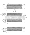
- the schematic diagram of FIG. 10A shows that the transport direction of the second optical member from which the release film has been peeled and the winding movement direction of the tape member coincide or substantially coincide.
- the schematic diagram of FIG. 10B shows that the winding movement direction of the tape member is substantially vertically downward with respect to the conveyance direction of the second optical member.
- the exclusion roller is disposed so as to protrude in the transport direction of the second optical member, and the tip portion of the second optical member adheres to the tape member that is stretched over the protrusion exclusion roller. Show. According to these configurations, since the feeding direction of the second optical member from the peeling device and the winding movement direction of the tape member substantially coincide, the second optical member can be suitably attached to the tape member. .
- the tape member winding movement speed is slower than the conveying speed of the second optical member, the tape member may be loosened and the second optical member may be wound around a machine such as another roll. . Therefore, these speeds are synchronized by this configuration, and this problem is suitably prevented.
- the “synchronization” may be completely coincident with no speed difference, or may be synchronization in consideration of apparatus error.
- the speed difference is in the range of ⁇ 3% to 3% of one of the speeds. Preferably, it may be in the range of -1% to 1%.
- the synchronization control method include a configuration in which the rotation speed of the winding roller of the tape member and the conveyance roller of the release film are controlled to be synchronized.
- a servo motor can be used for rotationally driving the take-up roller and the transport roller, and the control device can perform synchronous control so that the servo motors rotate simultaneously at the same speed.
- the (n + 1) th second optical member is the nth second optical member.
- the winding is stopped after the tape member is wound up to a position where at least a part of the optical member does not overlap.
- the second optical member can be prevented from falling off, and waste of the tape member or the like can be prevented.
- a gap between the nth (n is a natural number) second optical member and the (n + 1) th second optical member is about 3 mm, for example, until a position where all do not overlap.
- the exclusion device has a configuration in which the second optical member is attached to the tape member at a position avoiding an upper position of the optical display unit.
- the attachment of the tape member and the second optical member is not performed at the upper position of the optical display unit, so that the attachment of foreign matter or the like to the surface of the optical display unit can be prevented.
- the optical display unit can be prevented from being damaged by configuring the tape member so as not to contact the optical display unit.
- Specific implementation methods include, for example, a method in which the operating position of the exclusion device is not located above the transport position of the optical display unit, or an optical display unit that is not positioned below the exclusion device during the exclusion process. There is a method of stopping the conveyance.
- the exclusion device has a configuration in which the second optical member is attached to the tape member at a position below the optical display unit.
- the attachment of the tape member and the second optical member is executed at a position below the optical display unit, so that it is possible to prevent the attachment of foreign matter or the like on the surface of the optical display unit.
- Specific implementation methods include, for example, a method of installing the exclusion device below the transport position of the optical display unit, or a tape so that the bonding position of the tape member and the second optical member is below the optical display unit. The method of setting the operation position of a member and the position of the 2nd optical member peeled from a release film is mentioned.
- the optical display device manufacturing system further includes a pair of application rollers for attaching the first optical member to the optical display unit, There is a configuration in which the second optical member is attached to the tape member by sandwiching the second optical member between one of the sticking rollers and the exclusion roller.
- the cost of the manufacturing system can be reduced by using one of the sticking rollers.
- the manufacturing system further includes a rotating means for rotating the peeling device,
- the peeling device attaches the first optical member to the optical display unit while peeling the release film from the first optical member when bonding the first optical member to the optical display unit. Configured to go to the bonding position to be combined, When removing the second optical member from the release film, the tip of the peeling device is rotated downward by the rotating means, and the release film is peeled from the second optical member by the peeling device, There exists a structure which makes the said 2nd optical member go to the exclusion position lower than the said bonding position, and makes the said 2nd optical member adhere to the said tape member.
- the rotation position of the peeling device is controlled by the rotating means that rotates the peeling device so that the first optical member from which the release film has been peeled is directed to the bonding position where the optical display unit is bonded. Moreover, it can control suitably so that a 2nd optical member may be turned to the exclusion position lower than a bonding position.
- other production methods of the present invention include: It is a manufacturing method of an optical display device including the pasting process which bonds the 1st optical member to an optical display unit,
- the manufacturing method includes an excluding step of excluding the second optical member from the long release film that conveys the first optical member and the second optical member that is an object to be excluded,
- the exclusion step includes A moving process for moving an exclusion roller around which the tape member fed from the tape member winding means is wound; An attachment process for attaching the second optical member to the tape member; And a winding process in which the tape member to which the second optical member is attached is wound by a winding means.
- the manufacturing method of the optical display device includes at least a long release film and a long optical member provided on the long release film before the exclusion step. And further comprising a cutting step of cutting the long optical member leaving the long release film in the long laminated optical member configured to have, The first optical member and the second optical member are obtained by cutting the long optical member while leaving the long release film in the cutting step.
- the second optical member is provided on the long release film via an adhesive layer
- the tape member has a non-adhesive surface;
- the said adhesion process has the structure which adheres a said 2nd optical member to the said non-adhesive surface through the said adhesive layer.
- the manufacturing method of the optical display device includes peeling the long release film from the second optical member by winding the long release film around a peeling device. There is a configuration further including a peeling process.
- the said bonding process peels the said long release film from the said 1st optical member by winding the said long release film on the said peeling apparatus.
- the said bonding process peels the said long release film from the said 1st optical member by winding the said long release film on the said peeling apparatus.
- a front portion of the second optical member sent out from the peeling device by the peeling process is attached to the winding means side of the tape member, and the second optical member
- the movement process has a configuration in which the removal roller is moved to a position where the rear portion of the tape member is attached to the tape member winding means side of the tape member.
- a configuration in which the winding movement speed of the tape member by the winding process is synchronized with the feeding speed of the second optical member that is fed from the peeling device by the peeling process. is there.
- the conveyance by the long release film is temporarily stopped.
- at least a front portion of the second optical member is attached to the tape member.
- the winding process is performed when the tape member to which the n-th (n is a natural number) second optical member is wound is wound. There is a configuration in which the winding is stopped after the two optical members wind up the tape member to a position where at least a part of the second optical member does not overlap the n-th second optical member.
- the attaching process has a configuration in which the second optical member is attached to the tape member at a position avoiding an upper position of the optical display unit.
- the attachment process has a configuration in which the second optical member is attached to the tape member at a position below the optical display unit.
- the said bonding process sandwiches the said 1st optical member in the said optical display unit by pinching
- the attachment process has a configuration in which the second optical member is attached to the tape member by sandwiching the second optical member between one of the sticking rollers and the exclusion roller.
- the method further comprises a rotating means for rotating the peeling device,
- the peeling device attaches the first optical member to the optical display unit while peeling the release film from the first optical member. Configured to go to the bonding position to be combined,
- the tip of the peeling device is rotated downward by the rotating means, and the release film is peeled from the second optical member by the peeling device.
- the second optical member is directed to an exclusion position lower than the bonding position, and the second optical member is attached to the tape member.
- a process of bonding a non-defective optical member to the optical display unit and a process of removing a defective optical member without bonding to the optical display unit, for example, are continuously performed. You can do it.
- the exclusion device may be provided on the floor side of the optical display unit, and the second optical member to be excluded can be easily collected.
- the exclusion device is provided on the ceiling side from the optical display unit, it is not easy to collect the object to be excluded.
- the present invention exhibits its effects.
- the direction of the tip of the knife edge of the peeling device can be rotated and the peeling device can be moved to the floor side away from the bonding position of the optical display unit.
- the peeling device can be moved to the floor side away from the bonding position of the optical display unit without rotating the direction of the tip of the knife edge of the peeling device.
- the direction of the tip of the knife edge of the peeling device is left as it is, and an exclusion roller is arranged at the tip of the knife edge of the peeling device,
- the release film is turned over and reversed by the edge so that the release film is peeled off from the object to be excluded, and the object to be removed is adhered to the adhesive surface of the tape member that is stretched around the exclusion roller.
- the object to be excluded is removed while being adhered by winding the member.
- the exclusion object can be attached to the tape member by moving the exclusion roller to the distal end portion of the knife edge without changing the direction of the distal end of the knife edge.
- the first optical member is bonded to both surfaces of the optical display unit.
- the peeling apparatus and the bonding apparatus can use the same configuration as described above.
- the exclusion device is disposed on the floor side of the optical display unit.
- the optical display unit is rotated 90 degrees so that the first optical member that has already been bonded and the first optical member that is newly bonded have a crossed Nicols relationship.
- the rotation mechanism is preferably provided in the transport mechanism of the optical display unit.
- the optical display device of the present invention has an optical display unit and a first optical member bonded to one or both sides of the optical display unit.
- the optical display device include a liquid crystal display device and an organic EL display device.
- the optical display unit include a glass substrate unit of a liquid crystal cell (sometimes referred to as a liquid crystal panel), an organic EL light emitting unit of an organic EL cell, and the like.
- the optical display unit is cleaned in advance before being bonded to the first optical member.
- the optical display device of the present invention There is a configuration further including an inspection step of inspecting a bonded state after the first optical member is bonded to the optical display unit on one side or both sides. And each process can be performed with the continuous production line.
- Inspection of bonding state includes, for example, inspection for misalignment, misalignment, bubble mixing, and the like between the first optical member and the optical display unit.
- defects means, for example, surface or internal dirt, scratches, pit-like special defects (sometimes referred to as nicks) biting foreign objects, bubbles, foreign objects, etc. Yes.
- the exclusion apparatus which excludes the exclusion object of the present invention is: An exclusion device for excluding an object to be excluded, A tape member; Tape member winding means around which the tape member is wound; An exclusion roller on which the tape member fed from the tape member winding means is stretched; A drive mechanism for moving the exclusion roller; Winding means for winding up the tape member stretched over the exclusion roller, The exclusion roller is moved, and the exclusion object is attached to the tape member and wound up.
- the exclusion roller is moved to the exclusion position, the tape member stretched over the exclusion roller is attached to the exclusion object to be excluded, and the attached exclusion object is wound together with the tape member by the winding means. Can be wound up. Therefore, it is possible to suitably exclude the object to be excluded with a simple device configuration. In addition, since deformation such as bending of a member other than the object to be excluded is not substantially caused, the member is not damaged. Further, unlike the tip of the peeling claw as in the prior art document 1, the cross section of the exclusion roller is not square (preferably a circular cross section), and is attached to the tape member that is stretched over the exclusion roller. Therefore, there is no fear of damaging the object to be excluded and other members.
- the exclusion object is configured to include at least a long release film and a long optical member provided on the long release film.
- the optical member obtained by cutting the long optical member while leaving the long release film in the long laminated optical member.
- the exclusion apparatus can exclude suitably the optical member which is a removal target object from the elongate release film which conveys an optical member.
- the exclusion object has an adhesive layer
- the tape member has a non-adhesive surface
- the exclusion device passes through the adhesive layer.
- a front part of the exclusion object is attached to the winding means side of the tape member, and a rear part of the exclusion object is the tape member winding of the tape member.
- the drive mechanism moves the exclusion roller at a position attached to the means side. For example, when the winding movement direction of the tape member is the same as the conveyance direction of the optical member of the object to be excluded, there is no need for the tape member and the optical member or the release film to rub against each other. There are no problems such as adhesive stains.
- the winding means when winding the tape member to which the nth (n is a natural number) exclusion object is wound, the n + 1th exclusion object.
- the exclusion method of the present invention is: An exclusion method for eliminating an exclusion object, A moving process for moving an exclusion roller around which the tape member fed from the tape member winding means is wound; An attachment process for attaching the object to be excluded to the tape member; A winding process in which the tape member to which the object to be excluded is attached is wound by a winding means.
- the exclusion object has an adhesive layer
- the tape member has a non-adhesive surface
- the said adhesion process has the structure which adheres the said exclusion target object to the said non-adhesive surface through the said adhesive layer.
- the moving process has a configuration in which the exclusion roller is moved.
- the (n + 1) th exclusion object becomes the nth exclusion object.
- the object to be excluded is a long release optical film and a long laminated optical member configured to have at least a long optical member provided on the long release film.
- FIG. 1 Flowchart of manufacturing method of optical display device of embodiment 1
- FIG. 2 The figure for demonstrating the manufacturing system of Embodiment 1.
- FIG. The figure for demonstrating the apparatus structure of a manufacturing system The figure for demonstrating the apparatus structure of a manufacturing system
- the figure for demonstrating the apparatus structure of a manufacturing system The figure for demonstrating an example of the laminated structure of a laminated optical member
- FIG. 1 shows a flowchart of a method for manufacturing the optical display device according to the first embodiment.
- FIG. 3 shows a main configuration of the optical display device manufacturing system according to the first embodiment.
- the manufacturing system of Embodiment 1 includes first and second pre-inspection peeling devices 13 and 23, and first and second release film laminating devices 15 and 25 in the configuration of the manufacturing system of Embodiment 2 to be described later. This is a configuration example that is not. Further, as another embodiment of the manufacturing system of the first embodiment, a configuration in which the first and second defect inspection devices 14 and 24 are not provided can be exemplified.
- the exclusion process by the 1st, 2nd exclusion apparatus 19 and 29 it is not limited to the case where the optical member (for example, polarizing plate with a surface protection film) determined as inferior goods is excluded,
- the optical member for example, polarizing plate with a surface protection film
- sampling of process inspection An example of the case of exclusion for sampling of quality inspection is also exemplified.
- optical display unit examples include a glass substrate unit of a liquid crystal cell and an organic EL light emitting unit.
- the optical member of the present invention may have a single-layer structure or a laminated structure in which a plurality of films are laminated.
- the member is exemplified.
- a transparent film for protection may be laminated
- an adhesive is formed on one surface of the optical member so as to be attached to the optical display unit, and a long release film is provided to protect the adhesive, and the optical member with the release film is provided.
- the optical member may have a surface protective film laminated on the outermost surface different from the surface on which the long release film is formed.
- the surface protective film and the optical member with a release film are referred to as sheet products.
- the optical member before being unrolled from the roll material and cut may be referred to as a long optical member.
- the optical member attached to the optical display unit W is referred to as a first optical member, and the optical member to be excluded without being attached to the optical display unit is referred to as a second optical member.
- Judgment of the object to be excluded may be based on a defect inspection result or may be based on an exclusion instruction by an operator. In the following, an example of determination based on a defect inspection result is shown.
- First roll original fabric preparation step (FIG. 1, S1).
- a long first sheet product (first laminated optical member) is prepared as a first roll.
- variety of a 1st roll original fabric is dependent on the bonding size to an optical display unit.
- the laminated structure of the first sheet product F1 includes an optical member F11, a first release film F12, and a surface protective film F13.
- the first optical member F11 includes a first polarizer F11a, a first film F11b having an adhesive layer (not shown) on one side thereof, and a second film having an adhesive layer (not shown) on the other side.
- the protective film may be comprised only in one surface at the optical member F11, and it can comprise so that the other direction may be protected with a release film through an adhesive layer.
- the first and second films F11b and F11c are, for example, polarizer protective films (for example, triacetyl cellulose film, PET film, etc.).
- the second film F11c is bonded to the optical display unit surface side via the first adhesive F14.
- a surface treatment can be applied to the first film F11b. Examples of the surface treatment include a hard coat treatment, an antireflection treatment, a treatment for the purpose of prevention of sticking, diffusion or antiglare, and the like.
- the first release film F12 is provided via the second film F11c and the first pressure-sensitive adhesive layer F14.
- the surface protection film F13 is provided through the 1st film F11b and the adhesive layer F15. Specific configurations of the first and second films F11b and F11c will be described later. Below, the laminated structure of a polarizer and a polarizer protective film may be called a polarizing plate.
- the following processes are performed in an isolated structure that is isolated in the factory, and the cleanliness is maintained. In particular, it is important that the cleanliness is maintained in the bonding step of bonding the optical member to the optical display unit.
- the first sheet product (first laminated optical member) F1 is fed out from the first roll stock prepared and installed, and is conveyed downstream.
- the first conveying device 12 that conveys the first sheet product F1 is configured by, for example, a nip roller pair, a tension roller, a rotation driving device, an accumulating device A, a sensor device, a control device, and the like.
- the defect inspection method includes a method of photographing and processing images with transmitted light and reflected light on both sides of the first sheet product F1, and an inspection polarizing film between the CCD camera and the inspection object.
- a method is mentioned. Note that a known method can be applied to the image processing algorithm, and for example, a defect can be detected by density determination by binarization processing.
- the defect information obtained by the first defect inspection apparatus 14 is linked together with the position information (for example, position coordinates), transmitted to the control apparatus 1, and contributes to a cutting method by the first cutting apparatus 16 described later. be able to.
- the first cutting device 16 leaves the first release film F12 (without cutting), and cuts the surface protective film F13, the pressure-sensitive adhesive layer F15, the optical member F11, and the first pressure-sensitive adhesive layer F14 into a predetermined size.
- the target optical member to be attached to the optical display unit W is the first optical member
- the optical member to be excluded is the second optical member.
- the cutting means include a laser device, a cutter, and other known cutting means. Based on the defect information obtained by the first defect inspection apparatus 14, the cutting is performed so as to avoid the defect. Thereby, the yield of an optical member improves significantly.
- the second optical member of the object to be excluded including the defect is excluded by a first rejecting device 19 described later, and is not attached to the optical display unit W.
- Non-defective product determination (FIG. 1, S5).
- the determination criteria for the non-defective product determination are set in advance, and are set according to, for example, the number of defects per predetermined area, the defect size, and the type of defect. Non-defective product judgment becomes more severe as the display performance with higher accuracy is required.
- First optical member bonding step (FIG. 1, S6-1). A bonding process of the optical member F11 (corresponding to the first optical member) determined to be non-defective by the defect inspection is performed.
- the first optical member F11 with the surface protective film F13 is bonded to the floor-side surface of the optical display unit W in a laid-down state. Thereby, the first optical member is bonded to one surface of the optical display unit W.
- the 1st optical member F11 from which the said 1st release film F12 was removed using the 1st bonding apparatus 18 is 1st. 1 It bonds to the optical display unit W through the adhesive layer F14. At the time of bonding, as will be described later, the first optical member F11 and the optical display unit W are sandwiched and pressed between a pressing roller 181 and a guide roller 182 that constitute a pair of bonding rollers.
- Second optical member removal step of the object to be excluded (FIG. 1, S6-2).
- the optical member F11 (corresponding to the second optical member) determined as a defective product by the defect inspection is excluded as an object to be excluded.
- a configuration example of the exclusion process will be described later.
- the cleaning step (FIG. 1, S7).
- the surface of the optical display unit W is cleaned by the polishing cleaning device 10 and the water cleaning device 11.
- the cleaned optical display unit W is transported to the first bonding apparatus 18 by the transport mechanism.
- the transport mechanism includes, for example, a transport roller, a transport direction switching mechanism, a rotation drive device, a sensor device, and a control device.
- first roll original fabric preparation step the first inspection step, the first cutting step, the first optical member bonding step, and the cleaning step are preferably performed on a continuous production line.
- the first optical member F11 is bonded to one surface of the optical display unit W.
- the manufacturing process which affixes an optical member on another surface similarly is demonstrated.
- an optical member attached to the optical display unit is referred to as a first optical member
- an optical member that is excluded without being attached to the optical display unit is referred to as a second optical member. Called.
- Second roll original fabric preparation step (FIG. 1, S11).
- a long second sheet product (second laminated optical member) F2 is prepared as a second roll.
- the second sheet product F2 includes an optical member F21, a second release film F22, and a surface protection film F23.
- the optical member F21 includes a second polarizer 21a, a third film F21b having an adhesive layer (not shown) on one side thereof, and a fourth film F21c having an adhesive layer (not shown) on the other side.
- the protective film may be comprised only in one surface at the optical member F21, and it can comprise so that the other direction may be protected with a release film through an adhesive layer.
- the third and fourth films F21b and F21c are, for example, polarizer protective films (for example, triacetyl cellulose film, PET film, etc.).
- the fourth film F21c is bonded to the optical display unit surface side via the second pressure-sensitive adhesive layer F24.
- the third film F21b can be subjected to a surface treatment. Examples of the surface treatment include a hard coat treatment, an antireflection treatment, a treatment for the purpose of prevention of sticking, diffusion or antiglare, and the like.
- the second release film F22 is provided via the fourth film F21c and the second pressure-sensitive adhesive layer F24.
- the surface protection film F23 is provided through the 3rd film F21b and the adhesive layer F25. Specific configurations of the third and fourth films F21b and F21c will be described later.
- the second sheet material F2 is fed out from the prepared and installed second roll, and is conveyed downstream.
- the second conveying device 22 that conveys the second sheet product F2 includes, for example, a nip roller pair, a tension roller, a rotation driving device, an accumulating device A, a sensor device, a control device, and the like.
- Second inspection step (FIG. 1, S13).
- the second sheet material F2 is inspected for defects using the second defect inspection device 24.
- the defect inspection method here is the same as the method using the first defect inspection apparatus described above.
- Second cutting step (FIG. 1, S14).
- the second cutting device 26 leaves the second release film F22 (without cutting), and cuts the surface protective film F23, the pressure-sensitive adhesive layer F25, the optical member F21, and the second pressure-sensitive adhesive layer F24 into a predetermined size.
- the target optical member to be attached to the optical display unit W is the first optical member
- the optical member to be excluded is the second optical member.
- the cutting means include a laser device, a cutter, and other known cutting means. Based on the information on the defect obtained by the second defect inspection apparatus 24, it is configured to cut so as to avoid the defect. Thereby, the yield of an optical member improves significantly.
- the optical member F ⁇ b> 21 that is an object to be excluded including defects is excluded by a second exclusion device 29 described later, and is not attached to the optical display unit W.
- Non-defective product determination (FIG. 1, S15). As a result of the defect inspection by the second defect inspection device 24, it is determined whether or not it is a non-defective product.
- the determination criteria for the non-defective product determination are set in advance, and are set according to, for example, the number of defects per predetermined area, the defect size, and the type of defect. Non-defective product judgment becomes more severe as the display performance with higher accuracy is required.
- First optical member bonding step (FIG. 1, S16-1). Bonding processing of the optical member F21 (corresponding to the first optical member) determined to be non-defective in the defect inspection is performed.
- the 1st optical member F21 with a surface protection film is affixed on the surface by the side of the ceiling of the optical display unit W1 in the state of lying down. Thereby, an optical member (with a surface protection film) is formed on both surfaces of the optical display unit W.
- the 1st optical member F21 from which the said 2nd release film F22 was removed using the 2nd bonding apparatus 28 is 1st. 2 It bonds together with the optical display unit W1 through the adhesive layer F24.
- the optical display unit W1 is rotated 90 degrees by the transport direction switching mechanism of the transport mechanism, and the polarizer of the first optical member F11 and the first optical member F21. In some cases, the polarizers have a crossed Nicols relationship.
- the first optical member F21 and the optical display unit W1 are sandwiched between a pair of pasting rollers (281, 282) to be pressure-bonded.
- the first optical member F11 is bonded to one surface of the optical display unit W
- the first optical member F21 is bonded to the other surface
- the optical display device W12 having the optical member (with a surface protective film) provided on both surfaces is manufactured. can do.
- Excluding step of removing the second optical member to be excluded (FIG. 1, S16-2).
- the optical member F21 (corresponding to the second optical member) determined as a defective product by the defect inspection is excluded as an object to be excluded.
- a configuration example of the exclusion process will be described later.
- the inspection device 30 inspects the optical display device W12 obtained by attaching the optical member to both surfaces of the optical display unit.
- the inspection method include a method of capturing an image and processing an image using reflected light on both surfaces of the optical display device W12.
- a method of installing a polarizing film for inspection between the CCD camera and the inspection object is also exemplified.
- the method of irradiating light from the one surface side of the optical display device W12, photographing the transmitted light image, analyzing the image, and detecting defects is exemplified. Note that a known method can be applied to the image processing algorithm, and for example, a defect can be detected by density determination by binarization processing.
- the non-defective product determination of the optical display device W12 is performed.
- the non-defective product determined optical display device W12 is transported to the next mounting process. If a defective product is determined, a rework process is performed, a new optical film is applied, and then inspected.If a good product is determined, the process proceeds to a mounting process. Discarded.
- the optical display device W12 can be suitably manufactured by executing the first optical member F11 bonding step and the first optical member F21 bonding step in a continuous production line.
- the optical member can be bonded to the optical display unit W in an environment in which cleanliness is ensured, and a high-quality optical display device W12 is manufactured. can do.
- defect information (defect coordinates, defect type, size, etc.) of the first and second sheet products is coded in a predetermined pitch unit (for example, 1000 mm). It may be attached as information (for example, QR code, barcode). In such a case, before the cutting, the code information is read and analyzed, and cut into a predetermined size in the first and second cutting steps so as to avoid the defective portion.
- the part including the defect is removed or bonded to a member that is not the optical display unit, and the non-defective sheet optical member cut to a predetermined size is bonded to the optical display unit.
- the yield of the optical member is significantly improved.
- FIG. 2 shows a flowchart of the manufacturing method of the optical display device according to the second embodiment.
- FIG. 4 shows a main configuration of the optical display device manufacturing system according to the second embodiment. A process similar to that of the first embodiment will be briefly described.
- First roll original fabric preparation step (FIG. 2, S1).
- a long first sheet product (first laminated optical member) F1 is prepared as a first roll original.
- the laminated structure of the first sheet product F1 is the same as that of the first embodiment shown in FIG.
- the first pre-inspection peeling device 13 peels the release film F12 from the conveyed first sheet product F1. Details of the peeling mechanism will be described later.
- the 1st fault inspection apparatus 14 test inspects the fault of the optical member with a surface protection film after a release film removal process. It is not necessary to consider the phase difference inherent in the release film F12 and the defects such as foreign matter or scratches attached to or inherent in the release film F12, and the optical member F11 can be inspected for defects.
- the method of defect inspection is as described above.
- the optical member F11 (corresponding to the second optical member), which is an object to be excluded including defects, is excluded by a first exclusion device 19 described later, and is not attached to the optical display unit W.
- the 1st release film bonding apparatus 15 bonds the release film H12 to the optical member F11 via the 1st adhesive layer F14 after a 1st fault test process. In order to maintain flatness, it is preferable to perform the bonding so that bubbles such as bubbles do not occur. The detail of the 1st release film bonding apparatus 15 is mentioned later.
- First cutting step (FIG. 2, S26).
- the first cutting device 16 does not cut the release film H12, and the surface protective film F13, the pressure-sensitive adhesive layer F15, the optical member F11, and the first pressure-sensitive adhesive layer F14 have a predetermined size.
- Disconnect examples include a laser device, a cutter, and other known cutting means.
- Non-defective product determination (FIG. 2, S27). As a result of the defect inspection by the first defect inspection apparatus 14, it is determined whether or not the product is a non-defective product.
- the determination criteria for the non-defective product determination are set in advance, and are set according to, for example, the number of defects per predetermined area, the defect size, and the type of defect. Non-defective product judgment becomes more severe as the display performance with higher accuracy is required.
- the 1st optical member F11 from which the said 1st release film F12 was removed using the 1st bonding apparatus 18 is 1st. 1 It is bonded to the optical display unit W through the adhesive layer F14. At the time of pasting, as will be described later, the first optical member F11 and the optical display unit W are sandwiched between a pair of pasting rollers (pressing roller 181 and guide roller 182) to be pressure-bonded.
- Second optical member exclusion step of the object to be excluded (FIG. 2, S28-2). Exclusion processing is performed on the optical member F11 (corresponding to the second optical member), which is an object to be excluded, which has been determined to be defective in the defect inspection. A configuration example of the exclusion process will be described later.
- Second roll original fabric preparation step (FIG. 2, S11).
- a long second sheet product (second laminated optical member) F2 is prepared as a second roll.
- the laminated structure of the second sheet product F2 has the configuration shown in FIG.
- Transfer process (FIG. 2, S12).
- the second sheet material F2 is fed out from the prepared and installed second roll, and is conveyed downstream.
- the second pre-inspection peeling device 23 peels the release film F22 from the second sheet product F2 being conveyed. Details of the peeling mechanism will be described later.
- Second defect inspection step (FIG. 2, S34).
- the method of defect inspection is as described above.
- the optical member F21 including the defect (corresponding to the second optical member) is excluded by a second exclusion device 29 described later, and is configured not to be attached to the optical display unit.
- the 2nd release film bonding apparatus 25 bonds the release film H22 to the optical member F21 through the 2nd adhesive layer F24 after a 2nd fault test process. In order to maintain flatness, it is preferable to perform the bonding so that bubbles such as bubbles do not occur. The detail of the 2nd release film bonding apparatus 25 is mentioned later.
- Second cutting step (FIG. 2, S36).
- the second cutting device 26 does not cut the release film H22, and the surface protective film F23, the pressure-sensitive adhesive layer F25, the optical member F21, and the second pressure-sensitive adhesive layer F24 have a predetermined size.
- Disconnect examples include a laser device, a cutter, and other known cutting means.
- Non-defective product determination (FIG. 2, S37). As a result of the defect inspection by the second defect inspection device 24, it is determined whether or not it is a non-defective product.
- the determination criteria for the non-defective product determination are set in advance, and are set according to, for example, the number of defects per predetermined area, defect size, and defect type. Non-defective product judgment becomes more severe as the display performance with higher accuracy is required.
- First optical member bonding step (FIG. 2, S38-1). Bonding processing of the optical member F21 (corresponding to the first optical member) determined to be non-defective in the defect inspection is performed. The first optical member F21 with the surface protective film is bonded to the ceiling side surface of the optical display unit in a laid-down state.
- the first optical member F21 (surface) from which the second release film F22 has been removed using the second bonding device 28 A protective film is attached) to the optical display unit W1 through the second pressure-sensitive adhesive layer F24.
- the optical display unit W1 is rotated 90 degree
- the F21 polarizer may be in a crossed Nicols relationship.
- the first optical member F21 and the optical display unit W1 are sandwiched between a pair of pasting rollers (281, 282) to be pressure-bonded.
- a pair of pasting rollers (281, 282)
- Second optical member exclusion step of the object to be excluded (FIG. 2, S38-2). Exclusion processing of the optical member F21 (corresponding to the second optical member) determined as defective by the defect inspection is performed. A configuration example of the exclusion process will be described later.
- the non-defective product of the optical display device W12 is determined.
- the non-defective product determined optical display device W12 is transported to the next mounting process. If a defective product is determined, a rework process is performed, a new optical member is applied, and then inspected. If a non-defective product is determined, the process proceeds to a mounting process. Discarded.
- the optical display device can be preferably manufactured by executing the bonding process of the first optical member F11 and the first optical member F21 bonding process on a continuous production line.
- the optical member can be bonded to the optical display unit in an environment in which cleanliness is ensured, and a high-quality optical display device is manufactured. Can do.
- FIG. 5 is a diagram showing the first peeling device 17, the first sticking device 18, and the first exclusion device 19.
- FIG. 6 is a view showing the second peeling device 27, the second sticking device 28, and the second exclusion device 29.
- FIG. 7 is a diagram for explaining the configuration of the first exclusion device 19 and the exclusion operation.
- the structure of the 1st exclusion apparatus 19 is not restrict
- the second exclusion device 29 has the same configuration as that of the first exclusion device 19, but the exclusion operation is different, and the exclusion operation will be described with reference to FIG. 8.
- the first roll raw material of the long first sheet product (first laminated optical member) F1 is installed on a roller mount device that is linked to a motor or the like so as to rotate freely or at a constant rotational speed.
- the rotation speed is set by the control device 1 and the drive is controlled.
- the first transport device 12 is a transport mechanism that transports the first sheet product F1 to the downstream side.
- the first transport device 12 is controlled by the control device 1.
- the first pre-inspection peeling device 13 is configured to peel the release film from the conveyed first sheet product F1 and to wind the release film on a winding device.
- the winding speed of the winding device is controlled by the control device 1.
- As a peeling mechanism for peeling the release film it has a knife edge part with a sharp tip, and the release film is wound around this knife edge part and transferred in reverse, thereby releasing the release film and releasing the mold. It is comprised so that the 1st sheet product F1 after peeling a film may be conveyed in a conveyance direction.
- the first defect inspection device 14 performs defect inspection after the release film is peeled off.
- the first defect inspection device 14 detects the defect by analyzing the image data captured by the CCD camera, and further calculates its position coordinates. The position coordinates of this defect are provided for the skip cut by the first cutting device 16 described later.
- the 1st release film bonding apparatus 15 bonds the release film H12 to the optical member F11 through the 1st adhesive layer F14 after a 1st fault test
- the release film H12 is unwound from the roll of the release film H12, and the release film H12 and the optical member F11 are sandwiched by one or a plurality of roller pairs, and are bonded together by applying a predetermined pressure with the roller pairs.
- the rotation speed, pressure control, and conveyance control of the roller pair are controlled by the control device 1.
- the 1st cutting device 16 does not cut
- the first cutting device 16 is, for example, a laser device. Based on the position coordinates of the defect detected in the first defect inspection process, the first cutting device 16 cuts to a predetermined size so as to avoid the defect portion. That is, the cut product including the defective portion is rejected as a defective product by the first rejecting device 19 in a subsequent process. Alternatively, the first cutting device 16 may continuously cut into a predetermined size while ignoring the existence of the defect. In this case, it can be configured to remove the portion without bonding in a bonding process described later. Control in this case also depends on the function of the control device 1.
- the first cutting device 16 is provided with a holding table that sucks and holds the first sheet product F1 from the ceiling surface side, and a laser device is provided below the floor side of the first sheet product F1.
- the first sheet product F1 is moved in parallel so that the laser is scanned in the width direction, and the first optical member F11, the first pressure-sensitive adhesive layer F14, the surface protective film F13, and the pressure-sensitive adhesive layer, leaving the uppermost release film H12.
- F15 is cut at a predetermined pitch in the conveying direction (hereinafter referred to as “half cut” as appropriate).
- the accumulation device of the transport mechanism is moved in the vertical direction so as not to stop the continuous transport of the downstream and upstream first sheet products F1. It is configured. This operation is also controlled by the control device 1.
- the 1st bonding apparatus 18 is optical display unit through the 1st adhesive layer F14 for the optical member F11 (with surface protection film) from which the release film H12 was peeled by the 1st peeling apparatus 17 after the said cutting process. Affix to W. Only the optical member F11 (corresponding to the first optical member) determined to be non-defective by the first inspection device 14 is bonded to the optical display unit W. The optical member F11 and the optical display unit W determined to be non-defective are conveyed in synchronization with the bonding position. As shown in FIG. 5, the optical member F ⁇ b> 11 and the optical display unit W are conveyed so as to overlap each other. This is realized by controlling the control device 1 so that the first transport device 12 (including the accumulation device) and the transport mechanism are interlocked.
- the optical member F11 is bonded to the surface of the optical display unit W by the pressing roller 181 and the guide roller 182.
- the control device 1 controls the pressing pressure and driving operation of the pressing roller 181 and the guide roller 182.
- the peeling mechanism 171 of the first peeling device 17 has a knife edge portion with a sharp tip, and the release film H12 is wrapped around the knife edge portion and transferred in reverse, thereby peeling the release film H12.
- the optical member F11 (with a surface protection film) after peeling off the release film H12 is configured to be sent out to the optical display unit W surface.
- the peeled release mold H12 is wound around a roll 172.
- the winding control of the roll 172 is controlled by the control device 1.
- the laminating mechanism is composed of a pressing roller 181 and a guide roller 182 disposed opposite thereto.
- the guide roller 182 is composed of a rubber roller that is rotationally driven by a motor, and is provided with a drive mechanism that can move the roller up and down.
- a pressing roller 181 made of a metal roller that is rotationally driven by a motor is provided immediately above the driving roller 181 with a drive mechanism that can move the roller up and down.
- the pressing roller 181 moves away from the bonding position so as to open a roller interval.
- both the guide roller 182 and the pressing roller 181 may be rubber rollers or metal rollers.
- the optical display unit W is cleaned by various cleaning devices and is transported by the transport mechanism.
- the transport control of this transport mechanism is also controlled by the control device 1.
- the 1st exclusion apparatus 19 which excludes the optical member (equivalent to a 2nd optical member) of the exclusion target object 200 is demonstrated.
- the operation of the first exclusion device 19 will be described with reference to FIG.
- the first exclusion device 19 is disposed on the floor side with respect to the optical display unit W.
- the exclusion roller 192 is moved to the exclusion position by a drive mechanism (not shown).
- a known drive mechanism can be used as the drive mechanism for driving the exclusion roller.
- An exclusion film 191 (corresponding to a tape member) is stretched over the exclusion roller 192.
- the exclusion film 191 is drawn out from the winding means of the exclusion film 191 and wound around the take-up roller 193 via the exclusion roller 192.
- an adhesive tape can be used instead of the exclusion film 191.
- the release film H12 is peeled from the second optical member (with the surface protective film) by the knife edge 171 of the first peeling device 17, and the second optical member is directed in the floor direction from the bonding position of the optical display unit W. Dodge. Then, the exclusion object 200 (second optical member with a surface protective film) is sandwiched between the pressing roller 181 and the exclusion roller 192, and the exclusion object 200 is attached to the exclusion film 191 using the first adhesive layer F14. The exclusion object 200 is excluded by winding up the exclusion film 191 with a winding roller 193 (corresponding to a winding means).
- the tip position of the knife edge 171 is rotated by the rotating means from the bonding position direction, and the tip position rotates to the floor surface side, so that the object 200 to be removed is moved from the bonding position of the optical display unit W to the floor direction. It is going.
- the transport of the optical display unit W is stopped (the transport mechanism includes an accumulation mechanism). ). Then, the pressing roller 181 moves downward to the exclusion position of the exclusion object 200.
- the knife edge 171 rotates, and the tip direction thereof is directed obliquely from the upper side to the floor side. This rotation angle is set according to the specification of the first sheet product F1, the conveyance speed, and the like.
- the exclusion roller 192 around which the exclusion film 191 is stretched moves to the position of the pressing roller 181.
- the release film H12 is peeled off by the knife edge 171, and the pressing target 181 and the exclusion roller 181 are attached so that the exclusion object 200 sent out at the same time is attached to the exclusion film 191 by the first adhesive layer F14. And 192.
- the exclusion object 200 is pressed against the exclusion roller 192 side by the pressing roller 181 and the exclusion object 200 is attached to the exclusion film 191 by the first adhesive layer F14. Then, the exclusion object 200 is wound around the winding roller 193 together with the exclusion film 191.
- the moving speed of the exclusion film 191 by the take-up roller 193 and the conveying speed of the exclusion object 200 are synchronized.
- a servo motor can be used for rotational driving of the take-up roller 193 and the conveyance roller (not shown) of the object 200 to be excluded, and the control device 1 can perform synchronous control by rotating each servo motor simultaneously at the same speed. . (6) After the exclusion object 200 is removed, the pressing roller 181, the exclusion roller 192, and the knife edge 171 return to the original positions. The above operation is controlled by the control device 1.
- FIG. (1) movement of the 2nd exclusion apparatus 29 is demonstrated using FIG. (1)
- the optical member F21 corresponding to the second optical member
- the conveyance of the optical display unit W1 is stopped.
- the conveyance by the long release film F23 is also stopped once.
- the accumulating mechanism is provided in the transport mechanism.
- the guide roller 282 moves vertically downward.
- the exclusion roller 292 on which the exclusion film 291 is stretched is moved to a bonding position, which is a fixed position of the guide roller 282, by the driving mechanism (movement process).
- the pressing roller 281 moves vertically downward.
- the pressing roller 281 presses the exclusion target object 200 against the exclusion roller 292 side, and attaches the front portion of the exclusion target object 200 to the non-viscous surface of the exclusion film 291 via the second adhesive layer F24 ( Adhesion treatment).
- Adhesion treatment Adhesion treatment
- the conveyance by the long release film F22 is resumed, and the winding by the winding roller 293 is started, and the exclusion object 200 is wound around the winding roller 293 (winding device) together with the exclusion film 291. Taken (winding process).
- the take-up moving speed of the exclusion film 291 by the take-up roller 293 is synchronized with the delivery speed of the exclusion object 200.
- a servo motor can be used for rotational driving of the take-up roller 293 and the conveying roller (not shown) of the object 200 to be excluded, and the control device 1 can perform synchronous control by rotating each servo motor simultaneously at the same speed.
- the exclusion film 291 to which the second optical member F21 is attached is wound up to a position where the entire second optical member F21 does not overlap, and then the winding stops.
- the pressing roller 281 moves up, the removal roller 292 returns to the original position, and the guide roller 282 returns to the original position.
- the above operation is controlled by the control device 1.
- the optical display unit W1 to which the first optical member F11 is attached is conveyed downstream, and the optical member F21 of the second sheet product (second laminated optical member) F2 is attached thereto.
- the description of the same device configuration will be briefly described.
- the optical display unit W1 is rotated 90 ° by the transport direction switching mechanism of the transport mechanism.
- the optical member F21 is bonded.
- each step is processed with the second sheet product F2 inverted (with the release film on the top surface), and the optical member F21 is replaced with the optical display unit. It is comprised so that it may stick together from the lower side of W1.
- the second roll raw material of the long second sheet product F2 is installed on a roller mount device that is linked to a motor or the like so as to rotate freely or at a constant rotational speed.
- the rotation speed is set by the control device 1 and the drive is controlled.
- the second transport device 22 is a transport mechanism that transports the second sheet product F2 to the downstream side.
- the second transport device 22 is controlled by the control device 1.
- the second pre-inspection peeling device 23 has a configuration in which the release film is peeled from the conveyed second sheet product F2 and wound on a winding device.
- the winding speed of the winding device is controlled by the control device 1.
- the tip has a sharp knife edge part, and a release film is wound around the knife edge part and reversed and transferred to peel off the release film and peel off the release film.
- the second sheet product F2 is configured to be conveyed in the conveyance direction.
- the second defect inspection device 24 performs defect inspection after the release film is peeled off.
- the second defect inspection device 24 analyzes the image data picked up by the CCD camera, detects the defect, and calculates its position coordinates. The position coordinates of this defect are provided for the skip cut by the second cutting device 26 described later.
- the second release film bonding apparatus 25 bonds the release film H22 to the optical member F21 via the second pressure-sensitive adhesive layer F24 after the second defect inspection.
- the release film H22 is unwound from the roll of the release film H22, and the release film H22 and the optical member F21 are sandwiched by one or a plurality of roller pairs, and are bonded together by applying a predetermined pressure with the roller pairs.
- the rotation speed, pressure control, and conveyance control of the roller pair are controlled by the control device 1.
- the second cutting device 26 leaves the release film H22 (without cutting), the optical member F21, the surface protective film F23, the second pressure-sensitive adhesive layer F24, and the pressure-sensitive adhesive.
- the layer F25 is cut into a predetermined size.
- the second cutting device 26 is, for example, a laser device. Based on the position coordinates of the defect detected in the second defect inspection process, the second cutting device 26 cuts to a predetermined size so as to avoid the defect portion. That is, the cut product including the defective portion is rejected as a defective product by the second rejection device 29 in a later process. Or the 2nd cutting device 26 may ignore the presence of a fault, and may cut continuously to a predetermined size. In this case, it can be configured such that the portion is removed without being bonded in the bonding process described later. Control in this case also depends on the function of the control device 1.
- the second cutting device 26 is provided with a holding table for sucking and holding the second sheet product F2 from the floor side, and a laser device is provided on the ceiling side of the second sheet product F2.
- the second sheet product F2 is moved in parallel so as to scan the laser in the width direction, and the optical member F21, the second pressure-sensitive adhesive layer F24, the surface protective film F23, and the pressure-sensitive adhesive layer F25 are left leaving the lowermost release film H22. Cut at a predetermined pitch in the conveying direction.
- the accumulation device of the transport mechanism is moved in the vertical direction so as not to stop the continuous transport of the downstream and upstream second sheet products F2. It is configured. This operation is also controlled by the control device 1.
- the 2nd bonding apparatus 28 is optical display unit W1 through the 2nd adhesive layer F24 for the optical member F21 (with surface protection film) by which the release film H22 was peeled by the 2nd peeling apparatus 27 after the cutting process.
- the optical member F ⁇ b> 21 is bonded to the surface of the optical display unit W ⁇ b> 1 by the pressing roller 281 and the guide roller 282 while being bonded.
- the control device 1 controls the pressing pressure and driving operation of the pressing roller 281 and the guide roller 282. Only the optical member F21 (corresponding to the first optical member) determined to be non-defective by the second inspection device 24 is bonded to the optical display unit W1.
- the optical member F21 determined to be non-defective and the optical display unit W1 are conveyed in synchronization with the bonding position. As shown in FIG. 6, it is conveyed so that each front-end
- the peeling mechanism 271 of the second peeling device 27 has a knife edge portion with a sharp tip, and the release film H22 is wound around the knife edge portion and reversely transferred to peel the release film H22.
- the first optical member F21 after peeling off the release film H22 is configured to be sent out to the surface of the optical display unit W1.
- the peeled release film H22 is wound up on a roll 272.
- the winding control of the roll 272 is controlled by the control device 1.
- the laminating mechanism is composed of a pressing roller 281 and a guide roller 282 arranged opposite to it.
- the guide roller 282 is composed of a rubber roller that is rotationally driven by a motor, and is arranged to be movable up and down.
- a pressing roller 281 made of a metal roller that is rotationally driven by a motor is disposed directly below it.
- the pressing roller 281 is moved to a lower position so as to open a roller interval.
- both the guide roller 282 and the pressing roller 281 may be rubber rollers or metal rollers.
- the optical display device W12 obtained by bonding the optical members F11 and F21 to the optical display unit W is transported to the inspection device 30.
- the inspection device 30 performs an inspection on both sides of the optical display device W12 that has been conveyed.
- the light source of the inspection device 30 irradiates vertically from the lower surface side of the optical display device W12, and the transmitted light image is captured as image data by the CCD camera of the inspection device 30.
- the surface of the optical display device W12 can be irradiated with a light source at a predetermined angle, and the reflected light image can be captured as image data by a CCD camera. Defects are image-processed and analyzed from these image data, and non-defective products are determined.
- the operation timing of each apparatus is calculated by, for example, a method of detecting by arranging a sensor at a predetermined position, or by detecting a rotary member of the transfer apparatus or the transfer mechanism with a rotary encoder or the like.
- the control device 1 may be realized by a cooperative action of a software program and hardware resources such as a CPU and a memory. In this case, a memory is stored in advance for the program software, processing procedure, various settings, and the like. Further, it can be configured by a dedicated circuit or firmware.
- the control apparatus 1 is the structure which controls each apparatus collectively, it is not restricted to this, A control part is provided for each apparatus, and according to the command from the control apparatus 1, each apparatus is provided.
- the control unit can also be configured to control the operation of each device.
- the optical member F11 (with the surface protective film) is attached from the lower surface of the optical display unit W
- the optical member F21 (with the surface protective film) is attached from the upper surface of the optical display unit W1.
- the first and second exclusion devices 19 and 29 are located below the transport path of the optical display units W and W1. Thereby, collection
- the optical display unit is laid on its side, and the optical member is attached from the floor side surface. Can be configured to attach.
- each treatment of dyeing, crosslinking and stretching of the polyvinyl alcohol film need not be performed separately and may be performed simultaneously, and the order of the treatments may be arbitrary.
- a polyvinyl alcohol film is immersed in a solution containing iodine or a dichroic dye, dyed by adsorbing iodine or a dichroic dye, washed, and stretched in a solution containing boric acid or borax. After uniaxial stretching at a magnification of 3 to 7 times, it is dried.
- the adhesive treatment between the polarizer and the transparent polarizer protective film that is the protective layer is not particularly limited, but for example, an adhesive made of a vinyl alcohol polymer, boric acid, borax, or glutaraldehyde Or an adhesive comprising at least a water-soluble crosslinking agent of a vinyl alcohol polymer such as melamine or oxalic acid.
- an adhesive layer is formed as a coating / drying layer or the like of an aqueous solution.
- other additives and a catalyst such as an acid can be blended as necessary.
- Polarizer protective layer Polarizer protective film
- An appropriate transparent film can be used for the polarizer protective layer provided on one side or both sides of the polarizer.
- a thermoplastic resin excellent in transparency, mechanical strength, thermal stability, moisture barrier property, isotropy, etc. is used.
- thermoplastic resins include cellulose resins such as triacetyl cellulose, polyester resins, polyethersulfone resins, polysulfone resins, polycarbonate resins, polyamide resins, polyimide resins, polyolefin resins, (meth) acrylic resins, cyclic Examples thereof include polyolefin resins (norbornene resins), polyarylate resins, polystyrene resins, polyvinyl alcohol resins, and mixtures thereof.
- a transparent protective film is bonded to one side of the polarizer by an adhesive layer.
- thermosetting resin such as a system or an ultraviolet curable resin
- a thermosetting resin such as a system or an ultraviolet curable resin
- the additive include an ultraviolet absorber, an antioxidant, a lubricant, a plasticizer, a release agent, a coloring inhibitor, a flame retardant, a nucleating agent, an antistatic agent, a pigment, and a coloring agent.
- the transparent protective film may be subjected to surface modification treatment in order to improve adhesiveness with a polarizer before applying an adhesive.
- Specific examples of the treatment include corona treatment, plasma treatment, flame treatment, ozone treatment, primer treatment, glow treatment, saponification treatment, and treatment with a coupling agent.
- an antistatic layer can be appropriately formed.
- the optical member according to the present invention can be exemplified by an optical film having a laminated structure in which various optical layers are laminated in practical use.
- the optical layer is not particularly limited, for example, on the surface of the transparent protective film that does not adhere the polarizer (the surface on which the adhesive coating layer is not provided), hard coat treatment or antireflection treatment, Examples thereof include a method of applying a surface treatment for the purpose of preventing sticking, diffusion or antiglare, and laminating an alignment liquid crystal layer for the purpose of viewing angle compensation or the like.
- one or two optical films are used for forming a liquid crystal display device such as a reflection plate, a semi-transmission plate, a retardation plate (including a wave plate ( ⁇ plate) such as 1/2 or 1/4). The pasted ones are also included.
- An example of the optical film laminated on the polarizer is a retardation plate.
- the retardation plate include a birefringent film obtained by uniaxially or biaxially stretching a polymer material, a liquid crystal polymer alignment film, and a liquid crystal polymer alignment layer supported by a film.
- the stretching treatment can be performed by, for example, a roll stretching method, a long gap stretching method, a tenter stretching method, a tubular stretching method, or the like.
- the stretching ratio is generally about 1.1 to 3 times in the case of uniaxial stretching.
- the thickness of the retardation plate is not particularly limited, but is generally 10 to 200 ⁇ m, preferably 20 to 100 ⁇ m.
- polymer material examples include polyvinyl alcohol, polyvinyl butyral, polymethyl vinyl ether, polyhydroxyethyl acrylate, hydroxyethyl cellulose, hydroxypropyl cellulose, methyl cellulose, polycarbonate, polyarylate, polysulfone, polyethylene terephthalate, polyethylene naphthalate, and polyethersulfone.
- the retardation plate may have an appropriate retardation according to the purpose of use, such as those for the purpose of compensating for various wavelength plates or birefringence of the liquid crystal layer, viewing angle, and the like. What laminated
- the polarizing plate according to the present invention and the laminated optical film member are provided with an adhesive layer for adhering to other members such as a liquid crystal cell.
- the pressure-sensitive adhesive layer is not particularly limited, but can be formed with a suitable pressure-sensitive adhesive according to the conventional type such as acrylic. Low moisture absorption and heat resistance due to prevention of foaming and peeling phenomenon due to moisture absorption, deterioration of optical characteristics due to thermal expansion difference, prevention of liquid crystal cell warpage, and formation of a high-quality and durable image display device. It is preferable that it is an adhesive layer excellent in property. Moreover, it can be set as the adhesion layer etc. which contain microparticles
- the adhesive layer may be provided on a necessary surface as necessary.
- a polarizing plate comprising a polarizer and a polarizer protective layer
- the adhesive layer is adhered to one or both surfaces of the polarizer protective layer as necessary.
- a layer may be provided.
- a release film (Release film)
- the exposed surface of the adhesive layer is temporarily covered with a release film (sometimes referred to as a separator) for the purpose of preventing contamination until it is put to practical use. Thereby, it can prevent contacting an adhesion layer in the usual handling state.
- a suitable thin leaf body such as a plastic film, rubber sheet, paper, cloth, non-woven fabric, net, foam sheet, metal foil, laminate thereof, and the like, silicone type or Appropriate conventional ones such as those coated with an appropriate release agent such as long-chain alkyl, fluorine-based, or molybdenum sulfide can be used.
- a surface protective film is formed on the polarizing plate opposite to the surface provided with the separator via a weak adhesive. Its main purpose is to prevent scratches and pollution.
- the surface protective film for example, plastic film, rubber sheet, paper, cloth, non-woven fabric, net, foamed sheet or metal foil, appropriate thin leaves such as laminates thereof, if necessary silicone type or long chain alkyl type, Appropriate ones according to the prior art such as those coated with an appropriate release agent such as fluorine-based or molybdenum sulfide can be used.
- the optical member of the present invention can be preferably used for forming various optical display devices such as liquid crystal display devices.
- the liquid crystal display device can be formed according to the conventional method. That is, a liquid crystal display device is generally formed by appropriately assembling components such as a liquid crystal cell (corresponding to an optical display unit), an optical film, and an illumination system as necessary, and incorporating a drive circuit. In the present invention, there is no particular limitation except that the optical film according to the present invention is used.
- the liquid crystal cell any type such as a TN type, an STN type, or a ⁇ type can be used.
Abstract
Description
光学表示ユニットに第1光学部材を貼り合わせるための光学表示装置の製造システムであって、
前記光学表示装置の製造システムは、前記第1光学部材および排除対象物である第2光学部材を搬送する長尺の離型フィルムから、当該第2光学部材を排除する排除装置を備え、
前記排除装置は、テープ部材と、
前記テープ部材が巻回されたテープ部材巻回手段と、
前記テープ部材巻回手段から繰り出された前記テープ部材が掛け渡された排除ローラと、
前記排除ローラを移動させる駆動機構と、
前記排除ローラに掛け渡された前記テープ部材を巻き取る巻取手段と、を有し、
前記排除ローラを移動させ、当該テープ部材に前記第2光学部材を付着させて巻き取るように構成されたものである。
前記光学表示装置の製造システムは、長尺の離型フィルム、および当該長尺の離型フィルム上に設けられた長尺の光学部材を少なくとも有して構成される長尺の積層光学部材において前記長尺の離型フィルムを残して前記長尺の光学部材を切断する切断装置をさらに備え、
前記第1光学部材および前記第2光学部材は、前記切断装置により前記長尺の光学部材を切断することで得られたものである。
前記第2光学部材は、前記長尺の離型フィルム上に粘着剤層を介して設けられ、
前記テープ部材は、非粘着性表面を有し、
前記排除装置は、前記粘着剤層を介して前記非粘着性表面に前記第2光学部材を付着させる構成である。
前記光学表示装置の製造システムは、前記長尺の離型フィルムを巻き掛けることで当該第2光学部材から当該長尺の離型フィルムを剥離する剥離装置をさらに備える構成がある。この構成によれば、剥離装置から第2光学部材が送り出されるため、排除の際、排除ローラを適切な位置に移動させることで、テープ部材と離型フィルムとを接触させることなく、テープ部材に第2光学部材を付着させることができる。すなわち、第1光学部材の損壊の懸念をより低減できる。
前記剥離装置は、光学表示ユニットに第1光学部材を貼り合わせる際に、前記長尺の離型フィルムを巻き掛けることで当該第1光学部材からも当該長尺の離型フィルムを剥離させる構成がある。剥離装置は、第1光学部材から離型フィルムを剥離する機能も兼ね備えているため、製造システム全体として機能設計面に優れ、製造システムのコスト低減効果も高い。
前記剥離装置から送り出された前記第2光学部材の前方部が当該テープ部材の前記巻取手段の側に付着され、当該第2光学部材の後方部が当該テープ部材の前記テープ部材巻回手段の側に付着される位置に、前記駆動機構は前記排除ローラを移動させる構成がある。例えば、図10(a)から(c)に示すように、第2光学部材の前方部がテープ部材の巻取手段の側に付着され、第2光学部材の後方部がテープ部材のテープ部材巻回手段の側に付着される。図10(a)の模式図は、離型フィルムが剥離された第2光学部材の搬送方向とテープ部材の巻取り移動方向が一致または略一致していることを示す。図10(b)の模式図は、第2光学部材の搬送方向に対してテープ部材の巻取り移動方向が略垂直下向きであることを示す。図10(c)の模式図は、第2光学部材の搬送方向に排除ローラが突出して配置され、第2光学部材の先端部分が突出した排除ローラに掛け渡されたテープ部材に付着することを示す。これらの構成によれば、剥離装置からの第2光学部材の送出方向とテープ部材の巻取り移動方向とが略一致しているため、第2光学部材をテープ部材に好適に付着させることができる。
前記巻取手段による前記テープ部材の巻取り移動速度と、前記剥離装置から送り出される前記第2光学部材の送出速度とを同期させる構成がある。テープ部材の巻取り移動速度と排除対象物の第2光学部材の搬送速度が異なると、速度差による歪みにより不具合が生じてしまう。不具合の例として、テープ部材の巻取り移動速度が第2光学部材の搬送速度より速い場合、テープ部材の破断、離型フィルムが引っ張られることにより、光学表示ユニットに対する第1光学部材の貼りズレが発生するおそれがあり、また、テープ部材の巻取り移動速度が第2光学部材の搬送速度より遅い場合、テープ部材の弛み、第2光学部材が他のロール等の機械等へ巻き付くことがある。そのため、本構成によってそれら速度を同期させ、この不具合を好適に防止する。「同期」は、速度差がなく完全に一致する場合もあれば、装置誤差を考慮した同期としてもよく、例えば、速度差がいずれか一方の速度の-3%~3%の範囲であってもよく、好ましくは-1%~1%の範囲であってもよい。同期制御の方法としては、テープ部材の巻取りローラと離型フィルムの搬送ローラの回転速度を同期させるように制御する構成が例示される。例えば、巻取りローラと搬送ローラの回転駆動にサーボモータを用い、制御装置でそれぞれのサーボモータを同時同速回転させるように同期制御することができる。
前記長尺の離型フィルム上から当該第2光学部材を排除する際、
前記剥離装置から前記第2光学部材の少なくとも前方部を送り出した状態で、前記長尺の離型フィルムによる搬送を一旦停止させ、
前記巻取手段による前記テープ部材の巻き取りを停止した状態で、当該テープ部材に、前記第2光学部材の少なくとも前方部を付着させるとともに、
前記巻取手段による前記テープ部材の巻き取りを開始する時期と同時期に、前記長尺の離型フィルムによる搬送を開始する構成がある。この構成によれば、上述のテープ部材の巻取り移動速度と第2光学部材の送出速度とを同期させる構成と同様の効果が得られる。
前記巻取手段は、第n個目(nは自然数)の第2光学部材が付着されたテープ部材を巻き取る際に、第n+1個目の第2光学部材が前記第n個目の第2光学部材と少なくとも一部が重ならなくなる位置まで当該テープ部材を巻き取った後、巻き取りを停止する構成がある。この構成によれば、第2光学部材の脱落防止をできるとともに、テープ部材等の浪費も防ぐことができる。また、より好ましくは、全部が重ならなくなる位置まで、例えば、第n個目(nは自然数)の第2光学部材と第n+1個目の第2光学部材との隙間が3mm程度空けるとよい。
前記排除装置は、前記光学表示ユニットの上方位置を避けた位置で、前記テープ部材に前記第2光学部材を付着させる構成がある。排除処理において、テープ部材と第2光学部材の付着を光学表示ユニットの上方位置で実行しないように構成することで、光学表示ユニット表面に異物等の付着を防止できる。また、テープ部材を光学表示ユニットに接触しないように構成することで光学表示ユニットの破損等を防止できる。具体的な実現方法としては、例えば、排除装置の動作位置が光学表示ユニットの搬送位置の上方とならないように配置する方法や、排除処理中において、排除装置の下方に位置しないように光学表示ユニットの搬送を停止させる方法が挙げられる。
前記排除装置は、前記光学表示ユニットよりも下方位置で、前記テープ部材に前記第2光学部材を付着させる構成がある。排除処理において、テープ部材と第2光学部材の付着を光学表示ユニットの下方位置で実行させるため、光学表示ユニット表面に異物等の付着を防止できる。具体的な実現方法としては、例えば、排除装置を光学表示ユニットの搬送位置よりも下方に設置する方法や、テープ部材と第2光学部材の貼り合わせ位置を光学表示ユニットの下方になるようにテープ部材の動作位置、離型フィルムから剥離される第2光学部材の位置を設定する方法が挙げられる。
前記光学表示装置の製造システムは、前記光学表示ユニットに前記第1光学部材を貼り合わせるための一対の貼付ローラをさらに備え、
前記第2光学部材を、前記貼付ローラの一方と前記排除ローラとの間に挟むことで、前記テープ部材に前記第2光学部材を付着させる構成がある。
前記剥離装置は、前記光学表示ユニットに前記第1光学部材を貼り合せる際に、前記第1光学部材から前記離型フィルムを剥離させつつ、前記第1光学部材を、前記光学表示ユニットとの貼り合せる貼合位置に向かわせるように構成し、
前記第2光学部材を前記離型フィルムから排除する際に、前記回転手段によって剥離装置の先端を下方向に回転させ、当該剥離装置によって前記第2光学部材から前記離型フィルムを剥離させつつ、当該第2光学部材を前記貼合位置よりも低い排除位置に向かわせ、当該第2光学部材を前記テープ部材に付着させる構成がある。
光学表示ユニットに第1光学部材を貼り合わせる貼合工程を含む光学表示装置の製造方法であって、
前記製造方法は、前記第1光学部材および排除対象物である第2光学部材を搬送する長尺の離型フィルムから、当該第2光学部材を排除する排除工程を含み、
前記排除工程は、
テープ部材巻回手段から繰り出されたテープ部材が巻き掛けられた排除ローラを移動させる移動処理と、
前記テープ部材に前記第2光学部材を付着させる付着処理と、
前記第2光学部材が付着された前記テープ部材を巻取手段により巻き取る巻取処理とを含む構成である。
前記第1光学部材および前記第2光学部材は、前記切断工程により前記長尺の離型フィルムを残して前記長尺の光学部材を切断することで得られたものである。
前記テープ部材は、非粘着性表面を有し、
前記付着処理は、前記粘着剤層を介して前記非粘着性表面に前記第2光学部材を付着させる構成がある。
前記剥離処理により前記剥離装置から前記第2光学部材の少なくとも前方部を送り出した状態で、前記長尺の離型フィルムによる搬送を一旦停止させ、
前記巻取処理による前記テープ部材の巻き取りを停止した状態で、当該テープ部材に、前記第2光学部材の少なくとも前方部を付着させるとともに、
前記巻取処理による前記テープ部材の巻き取りを開始する時期と同時期に、前記長尺の離型フィルムによる搬送を開始する構成がある。
前記付着処理は、前記第2光学部材を、前記貼付ローラの一方と前記排除ローラとの間に挟むことで、前記テープ部材に前記第2光学部材を付着させる構成がある。
前記剥離装置は、前記光学表示ユニットに前記第1光学部材を貼り合せる工程において、前記第1光学部材から前記離型フィルムを剥離させつつ、前記第1光学部材を、前記光学表示ユニットとの貼り合せる貼合位置に向かわせるように構成し、
前記第2光学部材を前記離型フィルムから排除する排除工程において、前記回転手段によって剥離装置の先端を下方向に回転させ、当該剥離装置によって前記第2光学部材から前記離型フィルムを剥離させつつ、当該第2光学部材を前記貼合位置よりも低い排除位置に向かわせ、当該第2光学部材を前記テープ部材に付着させる構成がある。
片面あるいは両面に第1光学部材を光学表示ユニットに貼り合せた後に、貼り合わせ状態を検査する検査工程を、さらに有する構成がある。そして、それぞれの工程を連続した製造ラインで実行することができる。「貼り合わせ状態の検査」は、例えば、第1光学部材と光学表示ユニットの貼り合わせのズレ、ヨレ、気泡混入等についての検査が例示される。
片面あるいは両面に第1光学部材を光学表示ユニットに貼り合せた後に、貼り合わせ後の欠点を検査する検査工程を、さらに有する構成がある。そして、それぞれの工程を連続した製造ラインで実行することができる。「欠点」は、例えば、表面又は内部の汚れ、傷、異物をかみ込んだ打痕状のひねったような特殊状欠点(クニックと称されることがある)、気泡、異物等を意味している。
排除対象物を排除するための排除装置であって、
テープ部材と、
前記テープ部材が巻回されたテープ部材巻回手段と、
前記テープ部材巻回手段から繰り出された前記テープ部材が掛け渡された排除ローラと、
前記排除ローラを移動させる駆動機構と、
前記排除ローラに掛け渡された前記テープ部材を巻き取る巻取手段と、を有し、
前記排除ローラを移動させ、当該テープ部材に前記排除対象物を付着させて巻き取るように構成されたことを特徴とする。
排除対象物を排除するための排除方法であって、
テープ部材巻回手段から繰り出されたテープ部材が巻き掛けられた排除ローラを移動させる移動処理と、
前記テープ部材に前記排除対象物を付着させる付着処理と、
前記排除対象物が付着された前記テープ部材を巻取手段により巻き取る巻取処理とを含む構成である。
前記排除対象物は、粘着剤層を有するものであり、
前記テープ部材は、非粘着性表面を有し、
前記付着処理は、前記粘着剤層を介して前記非粘着性表面に前記排除対象物を付着させる構成がある。
前記排除対象物の前方部が前記テープ部材の前記巻取手段の側に付着され、当該排除対象物の後方部が当該テープ部材の前記テープ部材巻回手段の側に付着される位置に、前記移動処理は前記排除ローラを移動させる構成がある。
前記巻取処理は、第n個目(nは自然数)の排除対象物が付着された前記テープ部材を巻き取る際に、第n+1個目の排除対象物が前記第n個目の排除対象物と少なくとも一部が重ならなくなる位置まで当該テープ部材を巻き取った後、巻き取りを停止する構成がある。
前記排除対象物は、長尺の離型フィルム、および当該長尺の離型フィルム上に設けられた長尺の光学部材を少なくとも有して構成される長尺の積層光学部材において前記長尺の離型フィルムを残して前記長尺の光学部材を切断することで得られた光学部材である構成がある。
F2 第2シート製品
F11 光学部材
F11a 第1偏光子
F11b 第1フィルム
F11c 第2フィルム
F12 第1離型フィルム
F13 表面保護フィルム
F14 第1粘着剤層
F21 光学部材
F21a 第2偏光子
F21b 第3フィルム
F21c 第4フィルム
F22 第2離型フィルム
F23 表面保護フィルム
F24 第2粘着剤層
200 排除対象物(第2光学部材)
W 光学表示ユニット
W12 光学表示装置
1 制御装置
10 研磨洗浄装置
11 水洗浄装置
12 第1搬送装置
13 第1検査前剥離装置
14 第1欠点検査装置
15 第1離型フィルム貼合装置
16 第1切断装置
17 第1剥離装置
18 第1貼合装置
19 第1排除装置
22 第2搬送装置
23 第2検査前剥離装置
24 第2欠点検査装置
25 第2離型フィルム貼合装置
26 第2切断装置
27 第2剥離装置
28 第2貼合装置
29 第2排除装置
181 押さえローラ
182 案内ローラ
191 排除用フィルム
192 排除ローラ
193 巻取ローラ
本発明の実施形態1について以下に説明する。図1に実施形態1の光学表示装置の製造方法のフローチャートを示す。図3に実施形態1における光学表示装置の製造システムの主要構成を示す。実施形態1の製造システムは、後述する実施形態2の製造システムの構成の内、第1、第2検査前剥離装置13、23、第1、第2離型フィルム貼合装置15、25を備えていない構成例である。また、実施形態1の製造システムの別実施形態として、第1、第2欠点検査装置14、24を備えていない構成も例示できる。また、第1、第2排除装置19、29による排除工程では、不良品として判定された光学部材(例えば表面保護フィルム付き偏光板)を排除する場合に限定されず、例えば、工程検査のサンプリング、品質検査のサンプリング等するために排除する場合も例示される。
まず、本発明に用いられる光学表示ユニットは、例えば、液晶セルのガラス基板ユニット、有機EL発光体ユニット等が挙げられる。
本発明の光学部材は、単層構造でもよく、複数のフィルムが積層された積層構造でもよく、例えば、偏光子、位相差フィルム、輝度向上フィルム、それらフィルムの2以上が積層された積層の光学部材が例示される。また、光学部材には、保護用の透明フィルムが積層される場合があり、例えば、偏光子を保護する機能を有する偏光子保護フィルムが挙げられる。また、光学部材の一方表面には、光学表示ユニットに貼り付けられるように、粘着剤が形成され、この粘着剤を保護するための長尺の離型フィルムが設けられ、離型フィルム付き光学部材(積層光学部材の一例に相当する)を構成する。また、光学部材は、長尺の離型フィルムが形成される表面と異なる最表面に表面保護フィルムが積層されていてもよい。以下において、表面保護フィルムおよび離型フィルム付き光学部材(積層光学部材の一例に相当する)をシート製品と称する。
以下の説明において、ロール原反から繰り出され切断処理される前の光学部材を長尺の光学部材を称することがある。また、光学表示ユニットWに貼り付けされる光学部材を第1光学部材と称し、光学表示ユニットに貼り付けされずに排除される排除対象物の光学部材を第2光学部材と称する。排除対象物の判断は、欠点検査結果に基づいてもよく、オペレータによる排除指示に基づいていてもよく、以下では欠点検査結果に基づいて判断される例を示す。
また、上記第1切断工程および第2切断工程の別実施形態を以下に説明する。この実施形態は、上記の第1検査工程、第2検査工程を備えていない場合に特に有効である。第1および第2ロール原反の幅方向の一方の端部には、所定ピッチ単位(例えば1000mm)に第1、第2シート製品の欠点情報(欠点座標、欠点の種類、サイズ等)がコード情報(例えばQRコード、バーコード)として付されている場合がある。このような場合、切断する前段階で、このコード情報を読み取り、解析して欠点部分を避けるように、第1、第2切断工程において所定サイズに切断する。そして、欠点を含む部分は除去あるいは光学表示ユニットではない部材に貼り合わせるように構成し、所定サイズに切断された良品判定の枚葉の光学部材を光学表示ユニットに貼り合わされるように構成する。これにより、光学部材の歩留まりが大幅に向上される。
本発明の実施形態2について以下に説明する。図2に実施形態2の光学表示装置の製造方法のフローチャートを示す。図4に実施形態2における光学表示装置の製造システムの主要構成を示す。実施形態1と同様の処理についは簡単に説明する。
以下に、実施形態2の製造方法を実現する好適な製造システムの一例について説明する。
排除対象物200の光学部材(第2光学部材に相当する)を排除する第1排除装置19について説明する。図7を用いて第1排除装置19の動作を説明する。この第1排除装置19は、光学表示ユニットWよりも床側に配置される。排除動作の場合、排除ローラ192を不図示の駆動機構で排除位置に移動させる。排除ローラを駆動する駆動機構は公知の駆動機構を用いることができる。排除ローラ192には排除用フィルム191(テープ部材に相当する)が掛け渡されている。排除用フィルム191は、排除用フィルム191の巻回手段から繰り出され、排除ローラ192を介して巻取りローラ193に巻き取られる構成である。また、別実施形態として、排除用フィルム191に代替し粘着テープを用いることができる。
(2)上記動作と連動して、ナイフエッジ171が回転し、その先端方向が斜め上方から床側に向く。この回転角度は、第1シート製品F1の仕様、搬送速度等により設定される。
(3)上記の(1)、(2)の動作と連動して、排除用フィルム191が掛け渡された排除ローラ192は押さえローラ181の位置まで移動する。
(4)ナイフエッジ171によって、離型フィルムH12が剥離され、同時に送り出された排除対象物200は、第1粘着剤層F14によって排除用フィルム191と付着されるように、押さえローラ181と排除ローラ192とで、挟まれる。
(5)押さえローラ181で、排除対象物200を排除ローラ192側に押さえつけて、排除対象物200を第1粘着剤層F14によって排除用フィルム191に貼り付ける。そして、排除用フィルム191とともに排除対象物200を巻取りローラ193に巻き取る。ここで、巻取りローラ193による排除用フィルム191の移動速度と、排除対象物200の搬送速度とが同期している。例えば、巻取りローラ193と排除対象物200の搬送ローラ(不図示)の回転駆動にサーボモータを用い、制御装置1でそれぞれのサーボモータを同時同速回転させるようにして同期制御することができる。
(6)排除対象物200を排除後、押さえローラ181、排除ローラ192、ナイフエッジ171は原位置に復帰する。以上の動作は、制御装置1によって制御される。
(1)例えば欠点が存在し不良品判定された排除対象物200の光学部材F21(第2光学部材に相当する)が貼り合わせ位置に搬送されてくると、光学表示ユニットW1の搬送送りが停止するとともに、剥離装置271から第2光学部材F21の前方部を送り出した状態で(剥離処理)、長尺の離型フィルムF23による搬送も1旦停止させる。(なお、搬送機構にアキュムレート機構が具備されている。)そして、案内ローラ282は垂直下方に移動する。
(2)次いで、排除用フィルム291が掛け渡された排除ローラ292は、駆動機構によって案内ローラ282の定位置である貼り合わせ位置に移動する(移動処理)。
(3)押さえローラ281は垂直下方に移動する。
(4)押さえローラ281は、排除対象物200を排除ローラ292側に押さえつけて、排除対象物200の前方部を第2粘着剤層F24を介して排除用フィルム291の非粘性表面に付着させる(付着処理)。そして、長尺の離型フィルムF22による搬送が再開されるとともに、巻取りローラ293による巻取りが開始され、排除対象物200は、排除用フィルム291とともに巻取りローラ293(巻取装置)に巻き取られる(巻取処理)。ここで、巻取りローラ293による排除用フィルム291の巻取り移動速度と、排除対象物200の送出速度とが同期している。例えば、巻取りローラ293と排除対象物200の搬送ローラ(不図示)の回転駆動にサーボモータを用い、制御装置1でそれぞれのサーボモータを同時同速回転させるようにして同期制御することができる。また、このとき、第2光学部材F21が付着された排除用フィルム291は、次の第2光学部材F21の全体が重ならなくなる位置まで巻き取られた後、巻取りが停止する。
(5)排除後、押さえローラ281は上昇し、排除ローラ292は原位置に復帰し、案内ローラ282は原位置に復帰する。以上の動作は、制御装置1によって制御される。
以上の製造システムにおいては、光学表示ユニットを横倒しに寝かせ、その床側の面から光学部材を貼り付ける構成であったが、これに制限されず、光学表示ユニットの天井面側から光学部材を貼り付けるように構成することができる。
ポリビニルアルコール系フィルムの染色、架橋、延伸の各処理は、別々に行う必要はなく同時に行ってもよく、また、各処理の順番も任意でよい。なお、ポリビニルアルコール系フィルムとして、膨潤処理を施したポリビニルアルコール系フィルムを用いてもよい。一般には、ポリビニルアルコール系フィルムを、ヨウ素や二色性色素を含む溶液に浸漬し、ヨウ素や二色性色素を吸着させて染色した後洗浄し、ホウ酸やホウ砂等を含む溶液中で延伸倍率3倍~7倍で一軸延伸した後、乾燥する。ヨウ素や二色性色素を含む溶液中で延伸した後、ホウ酸やホウ砂等を含む溶液中でさらに延伸(二段延伸)した後、乾燥することにより、ヨウ素の配向が高くなり、偏光度特性が良くなるため、特に好ましい。
偏光子の片側又は両側に設ける偏光子保護層には、適宜な透明フィルムを用いることができる。例えば透明性、機械的強度、熱安定性、水分遮断性、等方性などに優れる熱可塑性樹脂が用いられる。このような熱可塑性樹脂の具体例としては、トリアセチルセルロース等のセルロース樹脂、ポリエステル樹脂、ポリエーテルスルホン樹脂、ポリスルホン樹脂、ポリカーボネイト樹脂、ポリアミド樹脂、ポリイミド樹脂、ポリオレフィン樹脂、(メタ)アクリル樹脂、環状ポリオレフィン樹脂(ノルボルネン系樹脂)、ポリアリレート樹脂、ポリスチレン樹脂、ポリビニルアルコール樹脂、およびこれらの混合物があげられる。なお、偏光子の片側には、透明保護フィルムが接着剤層により貼り合わされるが、他の片側には、透明保護フィルムとして、(メタ)アクリル系、ウレタン系、アクリルウレタン系、エポキシ系、シリコーン系等の熱硬化性樹脂または紫外線硬化型樹脂を用いることができる。透明保護フィルム中には任意の適切な添加剤が1種類以上含まれていてもよい。添加剤としては、例えば、紫外線吸収剤、酸化防止剤、滑剤、可塑剤、離型剤、着色防止剤、難燃剤、核剤、帯電防止剤、顔料、着色剤などがあげられる。
偏光子に積層される光学フィルムの一例として位相差板が挙げられる。位相差板としては、高分子材料を一軸または二軸延伸処理してなる複屈折性フィルム、液晶ポリマーの配向フィルム、液晶ポリマーの配向層をフィルムにて支持したものなどがあげられる。延伸処理は、例えばロール延伸法、長間隙沿延伸法、テンター延伸法、チューブラー延伸法などにより行うことができる。延伸倍率は、一軸延伸の場合には1.1~3倍程度が一般的である。位相差板の厚さも特に制限されないが、一般的には10~200μm、好ましくは20~100μmである。
本発明による偏光板や、前記の積層光学フィルム部材には、液晶セル等の他部材と接着するための粘着層が設けられる。その粘着層は、特に限定されるものではないが、アクリル系等の従来に準じた適宜な粘着剤にて形成することができる。吸湿による発泡現象や剥がれ現象の防止、熱膨脹差等による光学特性の低下や液晶セルの反り防止、ひいては高品質で耐久性に優れる画像表示装置の形成性等の点により、吸湿率が低くて耐熱性に優れる粘着層であることが好ましい。また、微粒子を含有して光拡散性を示す粘着層などとすることができる。粘着層は必要に応じて必要な面に設ければよく、例えば、偏光子と偏光子保護層からなる偏光板について言及するならば、必要に応じて、偏光子保護層の片面または両面に粘着層を設ければよい。
前記粘着層の露出面に対しては、実用に供するまでの間、その汚染防止等を目的に離型フィルム(セパレータと称することがある。)が仮着されてカバーされる。これにより、通例の取扱状態で粘着層に接触することを防止できる。セパレータとしては、上記厚さ条件を除き、例えばプラスチックフィルム、ゴムシート、紙、布、不織布、ネット、発泡シートや金属箔、それらのラミネート体等の適宜な薄葉体を、必要に応じシリコーン系や長鎖アルキル系、フッ素系や硫化モリブデン等の適宜な剥離剤でコート処理したものなどの、従来に準じた適宜なものを用いうる。
このセパレータが設けられた面と反対面の偏光板には、表面保護フィルムが弱粘着剤を介して形成される。その目的は、傷防止、汚染防止等が主目的である。表面保護フィルムとしては、例えばプラスチックフィルム、ゴムシート、紙、布、不織布、ネット、発泡シートや金属箔、それらのラミネート体等の適宜な薄葉体を、必要に応じシリコーン系や長鎖アルキル系、フッ素系や硫化モリブデン等の適宜な剥離剤でコート処理したものなどの、従来に準じた適宜なものを用いうる。
本発明の光学部材は液晶表示装置等の各種光学表示装置の形成などに好ましく用いることができる。液晶表示装置の形成は、従来に準じて行いうる。すなわち液晶表示装置は一般に、液晶セル(光学表示ユニットに相当する。)と光学フィルム、及び必要に応じての照明システム等の構成部品を適宜に組立てて駆動回路を組込むことなどにより形成されるが、本発明においては本発明による光学フィルムを用いる点を除いて特に限定はなく、従来に準じうる。液晶セルについても、例えばTN型やSTN型、π型などの任意なタイプのものを用いうる。
Claims (34)
- 光学表示ユニットに第1光学部材を貼り合わせるための光学表示装置の製造システムであって、
前記光学表示装置の製造システムは、前記第1光学部材および排除対象物である第2光学部材を搬送する長尺の離型フィルムから、当該第2光学部材を排除する排除装置を備え、
前記排除装置は、
テープ部材と、
前記テープ部材が巻回されたテープ部材巻回手段と、
前記テープ部材巻回手段から繰り出された前記テープ部材が掛け渡された排除ローラと、
前記排除ローラを移動させる駆動機構と、
前記排除ローラに掛け渡された前記テープ部材を巻き取る巻取手段と、を有し、
前記排除ローラを移動させ、当該テープ部材に前記第2光学部材を付着させて巻き取るように構成された、光学表示装置の製造システム。 - 前記光学表示装置の製造システムは、長尺の離型フィルム、および当該長尺の離型フィルム上に設けられた長尺の光学部材を少なくとも有して構成される長尺の積層光学部材において前記長尺の離型フィルムを残して前記長尺の光学部材を切断する切断装置をさらに備え、
前記第1光学部材および前記第2光学部材は、前記切断装置により前記長尺の光学部材を切断することで得られたものである、請求項1に記載の光学表示装置の製造システム。 - 前記第2光学部材は、前記長尺の離型フィルム上に粘着剤層を介して設けられ、
前記テープ部材は、非粘着性表面を有し、
前記排除装置は、前記粘着剤層を介して前記非粘着性表面に前記第2光学部材を付着させる、請求項1または2に記載の光学表示装置の製造システム。 - 前記光学表示装置の製造システムは、前記長尺の離型フィルムを巻き掛けることで当該第2光学部材から当該長尺の離型フィルムを剥離する剥離装置をさらに備える、請求項1から3のいずれかに記載の光学表示装置の製造システム。
- 前記剥離装置は、光学表示ユニットに第1光学部材を貼り合わせる際に、前記長尺の離型フィルムを巻き掛けることで当該第1光学部材からも当該長尺の離型フィルムを剥離させる、請求項4に記載の光学表示装置の製造システム。
- 前記剥離装置から送り出された前記第2光学部材の前方部が当該テープ部材の前記巻取手段の側に付着され、当該第2光学部材の後方部が当該テープ部材の前記テープ部材巻回手段の側に付着される位置に、前記駆動機構は前記排除ローラを移動させる、請求項4または5に記載の光学表示装置の製造システム。
- 前記巻取手段による前記テープ部材の巻取り移動速度と、前記剥離装置から送り出される前記第2光学部材の送出速度とを同期させる、請求項4から6のいずれかに記載の光学表示装置の製造システム。
- 前記長尺の離型フィルム上から前記第2光学部材を排除する際、
前記剥離装置から前記第2光学部材の少なくとも前方部を送り出した状態で、前記長尺の離型フィルムによる搬送を一旦停止させ、
前記巻取手段による前記テープ部材の巻き取りを停止した状態で、当該テープ部材に、前記第2光学部材の少なくとも前方部を付着させるとともに、
前記巻取手段による前記テープ部材の巻き取りを開始する時期と同時期に、前記長尺の離型フィルムによる搬送を開始する、請求項4から7のいずれかに記載の光学表示装置の製造システム。 - 前記巻取手段は、第n個目(nは自然数)の第2光学部材が付着されたテープ部材を巻き取る際に、第n+1個目の第2光学部材が前記第n個目の第2光学部材と少なくとも一部が重ならなくなる位置まで当該テープ部材を巻き取った後、巻き取りを停止する、請求項1から8のいずれかに記載の光学表示装置の製造システム。
- 前記排除装置は、前記光学表示ユニットの上方位置を避けた位置で、前記テープ部材に前記第2光学部材を付着させる、請求項1から9のいずれかに記載の光学表示装置の製造システム。
- 前記排除装置は、前記光学表示ユニットよりも下方位置で、前記テープ部材に前記第2光学部材を付着させる、請求項1から10のいずれかに記載の光学表示装置の製造システム。
- 前記光学表示装置の製造システムは、前記光学表示ユニットに前記第1光学部材を貼り合わせるための一対の貼付ローラをさらに備え、
前記第2光学部材を、前記貼付ローラの一方と前記排除ローラとの間に挟むことで、前記テープ部材に前記第2光学部材を付着させる、請求項1から11のいずれかに記載の光学表示装置の製造システム。 - 光学表示ユニットに第1光学部材を貼り合わせる貼合工程を含む光学表示装置の製造方法であって、
前記製造方法は、前記第1光学部材および排除対象物である第2光学部材を搬送する長尺の離型フィルムから、当該第2光学部材を排除する排除工程を含み、
前記排除工程は、
テープ部材巻回手段から繰り出されたテープ部材が巻き掛けられた排除ローラを移動させる移動処理と、
前記テープ部材に前記第2光学部材を付着させる付着処理と、
前記第2光学部材が付着された前記テープ部材を巻取手段により巻き取る巻取処理とを含む、光学表示装置の製造方法。 - 前記光学表示装置の製造方法は、前記排除工程の前に、長尺の離型フィルム、および当該長尺の離型フィルム上に設けられた長尺の光学部材を少なくとも有して構成される長尺の積層光学部材において前記長尺の離型フィルムを残して前記長尺の光学部材を切断する切断工程をさらに含み、
前記第1光学部材および前記第2光学部材は、前記切断工程により前記長尺の離型フィルムを残して前記長尺の光学部材を切断することで得られたものである、請求項13に記載の光学表示装置の製造方法。 - 前記第2光学部材は、前記長尺の離型フィルム上に粘着剤層を介して設けられ、
前記テープ部材は、非粘着性表面を有し、
前記付着処理は、前記粘着剤層を介して前記非粘着性表面に前記第2光学部材を付着させる、請求項13または14に記載の光学表示装置の製造方法。 - 前記光学表示装置の製造方法は、前記長尺の離型フィルムを剥離装置に巻き掛けることで前記第2光学部材から当該長尺の離型フィルムを剥離する剥離処理をさらに含む、請求項13から15のいずれかに記載の光学表示装置の製造方法。
- 前記貼合工程は、前記長尺の離型フィルムを前記剥離装置に巻き掛けることで前記第1光学部材から当該長尺の離型フィルムを剥離する第1光学部材剥離処理をさらに含む、請求項16に記載の光学表示装置の製造方法。
- 前記剥離処理により前記剥離装置から送り出された前記第2光学部材の前方部が当該テープ部材の前記巻取手段の側に付着され、当該第2光学部材の後方部が当該テープ部材の前記テープ部材巻回手段の側に付着される位置に、前記移動処理は前記排除ローラを移動させる、請求項16または17に記載の光学表示装置の製造方法。
- 前記巻取処理による前記テープ部材の巻取り移動速度と、前記剥離処理により前記剥離装置から送り出される前記第2光学部材の送出速度とを同期させる、請求項16から18のいずれかに記載の光学表示装置の製造方法。
- 前記長尺の離型フィルム上から当該第2光学部材を排除する際、
前記剥離処理により前記剥離装置から前記第2光学部材の少なくとも前方部を送り出した状態で、前記長尺の離型フィルムによる搬送を一旦停止させ、
前記巻取処理による前記テープ部材の巻き取りを停止した状態で、当該テープ部材に、前記第2光学部材の少なくとも前方部を付着させるとともに、
前記巻取処理による前記テープ部材の巻き取りを開始する時期と同時期に、前記長尺の離型フィルムによる搬送を開始する、請求項16から19のいずれかに記載の光学表示装置の製造方法。 - 前記巻取処理は、第n個目(nは自然数)の第2光学部材が付着された前記テープ部材を巻き取る際に、第n+1個目の第2光学部材が前記第n個目の第2光学部材と少なくとも一部が重ならなくなる位置まで当該テープ部材を巻き取った後、巻き取りを停止する、請求項13から20のいずれかに記載の光学表示装置の製造方法。
- 前記付着処理は、前記光学表示ユニットの上方位置を避けた位置で、前記テープ部材に前記第2光学部材を付着させる、請求項13から21のいずれかに記載の光学表示装置の製造方法。
- 前記付着処理は、前記光学表示ユニットよりも下方位置で、前記テープ部材に前記第2光学部材を付着させる、請求項13から22のいずれかに記載の光学表示装置の製造方法。
- 前記貼合工程は、前記光学表示ユニットおよび前記第1光学部材を一対の貼付ローラ間に挟みこむことで、前記光学表示ユニットに前記第1光学部材を貼り合わせるものであり、
前記付着処理は、前記第2光学部材を、前記貼付ローラの一方と前記排除ローラとの間に挟むことで、前記テープ部材に前記第2光学部材を付着させる、請求項13から23のいずれかに記載の光学表示装置の製造方法。 - 排除対象物を排除するための排除装置であって、
テープ部材と、
前記テープ部材が巻回されたテープ部材巻回手段と、
前記テープ部材巻回手段から繰り出された前記テープ部材が掛け渡された排除ローラと、
前記排除ローラを移動させる駆動機構と、
前記排除ローラに掛け渡された前記テープ部材を巻き取る巻取手段と、を有し、
前記排除ローラを移動させ、当該テープ部材に前記排除対象物を付着させて巻き取るように構成された、排除装置。 - 前記排除対象物は、粘着剤層を有するものであり、
前記テープ部材は、非粘着性表面を有し、
前記排除装置は、前記粘着剤層を介して前記非粘着性表面に前記排除対象物を付着させる、請求項25に記載の排除装置。 - 前記排除対象物の前方部が前記テープ部材の前記巻取手段の側に付着され、当該排除対象物の後方部が当該テープ部材の前記テープ部材巻回手段の側に付着される位置に、前記駆動機構は前記排除ローラを移動させる、請求項25または26に記載の排除装置。
- 前記巻取手段は、第n個目(nは自然数)の排除対象物が付着された前記テープ部材を巻き取る際に、第n+1個目の排除対象物が前記第n個目の排除対象物と少なくとも一部が重ならなくなる位置まで当該テープ部材を巻き取った後、巻き取りを停止する、請求項25から27のいずれかに記載の排除装置。
- 前記排除対象物は、長尺の離型フィルム、および当該長尺の離型フィルム上に設けられた長尺の光学部材を少なくとも有して構成される長尺の積層光学部材において前記長尺の離型フィルムを残して前記長尺の光学部材を切断することで得られた光学部材である、請求項25から28のいずれかに記載の排除装置。
- 排除対象物を排除するための排除方法であって、
テープ部材巻回手段から繰り出されたテープ部材が巻き掛けられた排除ローラを移動させる移動処理と、
前記テープ部材に前記排除対象物を付着させる付着処理と、
前記排除対象物が付着された前記テープ部材を巻取手段により巻き取る巻取処理とを含む、排除方法。 - 前記排除対象物は、粘着剤層を有するものであり、
前記テープ部材は、非粘着性表面を有し、
前記付着処理は、前記粘着剤層を介して前記非粘着性表面に前記排除対象物を付着させる、請求項30に記載の排除方法。 - 前記排除対象物の前方部が前記テープ部材の前記巻取手段の側に付着され、当該排除対象物の後方部が当該テープ部材の前記テープ部材巻回手段の側に付着される位置に、前記移動処理は前記排除ローラを移動させる、請求項30または31に記載の排除方法。
- 前記巻取処理は、第n個目(nは自然数)の排除対象物が付着された前記テープ部材を巻き取る際に、第n+1個目の排除対象物が前記第n個目の排除対象物と少なくとも一部が重ならなくなる位置まで当該テープ部材を巻き取った後、巻き取りを停止する、請求項30から32のいずれかに記載の排除方法。
- 前記排除対象物は、長尺の離型フィルム、および当該長尺の離型フィルム上に設けられた長尺の光学部材を少なくとも有して構成される長尺の積層光学部材において前記長尺の離型フィルムを残して前記長尺の光学部材を切断することで得られた光学部材である、請求項30から33のいずれかに記載の排除方法。
Priority Applications (4)
| Application Number | Priority Date | Filing Date | Title |
|---|---|---|---|
| EP09731115.3A EP2246835B1 (en) | 2008-04-08 | 2009-04-07 | Manufacturing system for an optical display device, manufacturing method for an optical display device, removal device, and removal method |
| PL09731115T PL2246835T3 (pl) | 2008-04-08 | 2009-04-07 | System do wytwarzania optycznego urządzenia wyświetlającego, sposób wytwarzania optycznego urządzenia wyświetlającego, oraz urządzenie usuwające i sposób usuwania |
| US12/865,284 US8057619B2 (en) | 2008-04-08 | 2009-04-07 | Manufacturing system for an optical display device, manufacturing method for an optical display device, excluding device and excluding method |
| CN2009801012412A CN101884060B (zh) | 2008-04-08 | 2009-04-07 | 光学显示装置的制造系统、光学显示装置的制造方法、排除装置及排除方法 |
Applications Claiming Priority (4)
| Application Number | Priority Date | Filing Date | Title |
|---|---|---|---|
| JP2008100622 | 2008-04-08 | ||
| JP2008-100622 | 2008-04-08 | ||
| JP2009092652A JP4551477B2 (ja) | 2008-04-08 | 2009-04-07 | 光学表示装置の製造システム、光学表示装置の製造方法、排除装置および排除方法 |
| JP2009-092652 | 2009-04-07 |
Publications (1)
| Publication Number | Publication Date |
|---|---|
| WO2009125771A1 true WO2009125771A1 (ja) | 2009-10-15 |
Family
ID=41161903
Family Applications (1)
| Application Number | Title | Priority Date | Filing Date |
|---|---|---|---|
| PCT/JP2009/057140 WO2009125771A1 (ja) | 2008-04-08 | 2009-04-07 | 光学表示装置の製造システム、光学表示装置の製造方法、排除装置および排除方法 |
Country Status (8)
| Country | Link |
|---|---|
| US (1) | US8057619B2 (ja) |
| EP (1) | EP2246835B1 (ja) |
| JP (1) | JP4551477B2 (ja) |
| KR (1) | KR101008418B1 (ja) |
| CN (1) | CN101884060B (ja) |
| PL (1) | PL2246835T3 (ja) |
| TW (1) | TW201007251A (ja) |
| WO (1) | WO2009125771A1 (ja) |
Cited By (5)
| Publication number | Priority date | Publication date | Assignee | Title |
|---|---|---|---|---|
| JP4844857B1 (ja) * | 2011-02-23 | 2011-12-28 | 住友化学株式会社 | 回収装置、貼合システム及び回収方法 |
| CN102298232A (zh) * | 2010-06-24 | 2011-12-28 | 日东电工株式会社 | 液晶显示面板的连续制造系统以及连续制造方法 |
| WO2012029716A1 (ja) * | 2010-09-02 | 2012-03-08 | 日東電工株式会社 | 連続ロール、並びに、液晶表示素子の製造方法及び製造システム |
| KR101169902B1 (ko) | 2011-02-23 | 2012-07-31 | 수미토모 케미칼 컴퍼니 리미티드 | 회수 장치, 접합 시스템 및 회수 방법 |
| WO2012147793A1 (ja) * | 2011-04-28 | 2012-11-01 | 住友化学株式会社 | ナイフエッジおよびこれを含む液晶表示装置の製造システム |
Families Citing this family (11)
| Publication number | Priority date | Publication date | Assignee | Title |
|---|---|---|---|---|
| WO2011105273A1 (ja) * | 2010-02-24 | 2011-09-01 | 住友化学株式会社 | 液晶表示装置の製造方法 |
| JP5181011B2 (ja) * | 2010-10-21 | 2013-04-10 | 日東電工株式会社 | 液晶表示素子の連続製造システムおよび液晶表示素子の連続製造方法 |
| JP5140788B2 (ja) * | 2010-11-22 | 2013-02-13 | 日東電工株式会社 | 液晶表示素子の連続製造システムおよび液晶表示素子の連続製造方法 |
| JP4750227B1 (ja) | 2011-01-14 | 2011-08-17 | 日東電工株式会社 | 液晶表示素子の連続製造システムおよび液晶表示素子の連続製造方法 |
| JP5068876B1 (ja) * | 2011-06-10 | 2012-11-07 | 日東電工株式会社 | 液晶表示素子の連続製造方法及び装置 |
| WO2013002187A1 (ja) * | 2011-06-29 | 2013-01-03 | 住友化学株式会社 | ナイフエッジおよびこれを含む液晶表示装置の製造システム |
| WO2013146883A1 (ja) | 2012-03-30 | 2013-10-03 | 日東電工株式会社 | 液晶表示装置の製造方法 |
| KR101318179B1 (ko) * | 2012-03-30 | 2013-10-16 | 주식회사 에스에프에이 | 릴투패널 편광필름 부착 장치 및 그 방법 |
| KR101932562B1 (ko) * | 2012-09-18 | 2018-12-28 | 삼성디스플레이 주식회사 | 필름 부착장치 및 그것을 이용한 필름 부착방법 |
| JP5724147B2 (ja) * | 2013-02-27 | 2015-05-27 | 住友化学株式会社 | 光学表示デバイスの生産システム |
| CA3219583A1 (en) * | 2016-08-10 | 2018-02-15 | Agc Engineering Co., Ltd. | Processing method of base material sheet, manufacturing method of modified base material sheet, base material with grafted polymer chain, and ion exchange membrane |
Citations (3)
| Publication number | Priority date | Publication date | Assignee | Title |
|---|---|---|---|---|
| JPS5752017A (en) | 1980-08-08 | 1982-03-27 | Sharp Corp | Tacky-polarizing-plate defective removing device automatic tacky-polarizing-plate sticking machine |
| JPH11333929A (ja) * | 1998-05-22 | 1999-12-07 | Somar Corp | フィルム張付装置における原反フィルムの連続的供給方法及び装置 |
| JP2007140046A (ja) * | 2005-11-17 | 2007-06-07 | Nitto Denko Corp | 光学表示装置の製造システム及びその製造方法 |
Family Cites Families (6)
| Publication number | Priority date | Publication date | Assignee | Title |
|---|---|---|---|---|
| KR100400399B1 (ko) * | 2001-11-23 | 2003-10-01 | 주식회사 엘지이아이 | 무전극 조명기기의 전등장치 |
| CN1297844C (zh) | 2001-11-27 | 2007-01-31 | 夏普株式会社 | 液晶板、液晶板制造方法、液晶板制造设备和偏振片粘结设备 |
| US7202923B2 (en) | 2001-11-27 | 2007-04-10 | Sharp Kabushiki Kaisha | Liquid crystal display with polarizer with inclined edge portion |
| CN1721935A (zh) * | 2004-07-13 | 2006-01-18 | 鸿富锦精密工业(深圳)有限公司 | 撕膜装置、偏光片贴附装置及撕膜方法 |
| CN101528445B (zh) * | 2006-10-17 | 2016-08-17 | 日东电工株式会社 | 光学构件贴合方法以及使用该方法的装置 |
| JP4724742B2 (ja) | 2008-01-09 | 2011-07-13 | 日東電工株式会社 | 光学表示装置の製造システムおよび光学表示装置の製造方法 |
-
2009
- 2009-04-07 EP EP09731115.3A patent/EP2246835B1/en active Active
- 2009-04-07 JP JP2009092652A patent/JP4551477B2/ja active Active
- 2009-04-07 WO PCT/JP2009/057140 patent/WO2009125771A1/ja active Application Filing
- 2009-04-07 CN CN2009801012412A patent/CN101884060B/zh active Active
- 2009-04-07 PL PL09731115T patent/PL2246835T3/pl unknown
- 2009-04-07 KR KR1020107007623A patent/KR101008418B1/ko active IP Right Grant
- 2009-04-07 US US12/865,284 patent/US8057619B2/en active Active
- 2009-04-08 TW TW098111713A patent/TW201007251A/zh unknown
Patent Citations (3)
| Publication number | Priority date | Publication date | Assignee | Title |
|---|---|---|---|---|
| JPS5752017A (en) | 1980-08-08 | 1982-03-27 | Sharp Corp | Tacky-polarizing-plate defective removing device automatic tacky-polarizing-plate sticking machine |
| JPH11333929A (ja) * | 1998-05-22 | 1999-12-07 | Somar Corp | フィルム張付装置における原反フィルムの連続的供給方法及び装置 |
| JP2007140046A (ja) * | 2005-11-17 | 2007-06-07 | Nitto Denko Corp | 光学表示装置の製造システム及びその製造方法 |
Non-Patent Citations (1)
| Title |
|---|
| See also references of EP2246835A4 * |
Cited By (9)
| Publication number | Priority date | Publication date | Assignee | Title |
|---|---|---|---|---|
| CN102298232A (zh) * | 2010-06-24 | 2011-12-28 | 日东电工株式会社 | 液晶显示面板的连续制造系统以及连续制造方法 |
| CN102298232B (zh) * | 2010-06-24 | 2012-08-29 | 日东电工株式会社 | 液晶显示面板的连续制造系统以及连续制造方法 |
| WO2012029716A1 (ja) * | 2010-09-02 | 2012-03-08 | 日東電工株式会社 | 連続ロール、並びに、液晶表示素子の製造方法及び製造システム |
| JP2012053349A (ja) * | 2010-09-02 | 2012-03-15 | Nitto Denko Corp | 連続ロール、並びに、液晶表示素子の製造方法及び製造システム |
| JP4844857B1 (ja) * | 2011-02-23 | 2011-12-28 | 住友化学株式会社 | 回収装置、貼合システム及び回収方法 |
| KR101169902B1 (ko) | 2011-02-23 | 2012-07-31 | 수미토모 케미칼 컴퍼니 리미티드 | 회수 장치, 접합 시스템 및 회수 방법 |
| WO2012114546A1 (ja) * | 2011-02-23 | 2012-08-30 | 住友化学株式会社 | 回収装置、貼合システム及び回収方法 |
| WO2012147793A1 (ja) * | 2011-04-28 | 2012-11-01 | 住友化学株式会社 | ナイフエッジおよびこれを含む液晶表示装置の製造システム |
| JP2012234014A (ja) * | 2011-04-28 | 2012-11-29 | Sumitomo Chemical Co Ltd | ナイフエッジおよびこれを含む液晶表示装置の製造システム |
Also Published As
| Publication number | Publication date |
|---|---|
| US8057619B2 (en) | 2011-11-15 |
| EP2246835B1 (en) | 2014-01-01 |
| CN101884060A (zh) | 2010-11-10 |
| JP2009271521A (ja) | 2009-11-19 |
| TW201007251A (en) | 2010-02-16 |
| KR101008418B1 (ko) | 2011-01-14 |
| EP2246835A4 (en) | 2011-03-16 |
| US20100326589A1 (en) | 2010-12-30 |
| JP4551477B2 (ja) | 2010-09-29 |
| PL2246835T3 (pl) | 2014-06-30 |
| TWI334038B (ja) | 2010-12-01 |
| KR20100086985A (ko) | 2010-08-02 |
| EP2246835A1 (en) | 2010-11-03 |
| CN101884060B (zh) | 2013-01-30 |
Similar Documents
| Publication | Publication Date | Title |
|---|---|---|
| JP4551477B2 (ja) | 光学表示装置の製造システム、光学表示装置の製造方法、排除装置および排除方法 | |
| JP5313002B2 (ja) | 光学表示装置の製造方法 | |
| JP4759091B2 (ja) | 光学表示装置の製造システムおよび光学表示装置の製造方法 | |
| TWI329751B (ja) | ||
| TWI497155B (zh) | Manufacturing system and manufacturing method of optical display device | |
| JP4568375B2 (ja) | 光学表示装置の製造方法及び製造システム | |
| JP4562792B2 (ja) | 連結シート製品の製造方法、連結シート製品および光学表示ユニットの製造方法 | |
| WO2010134441A1 (ja) | 光学表示装置の製造システム及び製造方法 | |
| JP4853877B2 (ja) | 連結シート製品の製造方法、連結シート製品および光学表示ユニットの製造方法 | |
| JP5792597B2 (ja) | 液晶表示素子の製造方法および液晶表示素子の製造システム | |
| JP2009282385A (ja) | 光学表示装置の製造方法 | |
| JP5181125B2 (ja) | 光学表示ユニットの検査方法およびその検査方法を用いた光学表示ユニットの製造方法 | |
| JP5244014B2 (ja) | 光学表示装置の製造方法 | |
| JP5461371B2 (ja) | 液晶表示素子の製造方法および液晶表示素子の製造システム | |
| JP2010026314A (ja) | 光学表示ユニットの製造方法 | |
| JP2011237757A (ja) | 光学表示装置の製造システム及び製造方法 | |
| WO2009096130A1 (ja) | 光学表示ユニットの製造方法および製造システム |
Legal Events
| Date | Code | Title | Description |
|---|---|---|---|
| WWE | Wipo information: entry into national phase |
Ref document number: 200980101241.2 Country of ref document: CN |
|
| 121 | Ep: the epo has been informed by wipo that ep was designated in this application |
Ref document number: 09731115 Country of ref document: EP Kind code of ref document: A1 |
|
| ENP | Entry into the national phase |
Ref document number: 20107007623 Country of ref document: KR Kind code of ref document: A |
|
| WWE | Wipo information: entry into national phase |
Ref document number: 12865284 Country of ref document: US |
|
| WWE | Wipo information: entry into national phase |
Ref document number: 2009731115 Country of ref document: EP |
|
| NENP | Non-entry into the national phase |
Ref country code: DE |