WO2009125620A1 - コンデンサおよびその製造方法 - Google Patents
コンデンサおよびその製造方法 Download PDFInfo
- Publication number
- WO2009125620A1 WO2009125620A1 PCT/JP2009/052136 JP2009052136W WO2009125620A1 WO 2009125620 A1 WO2009125620 A1 WO 2009125620A1 JP 2009052136 W JP2009052136 W JP 2009052136W WO 2009125620 A1 WO2009125620 A1 WO 2009125620A1
- Authority
- WO
- WIPO (PCT)
- Prior art keywords
- plating
- film
- capacitor
- dielectric film
- conductive substrate
- Prior art date
Links
Images


Classifications
-
- H—ELECTRICITY
- H01—ELECTRIC ELEMENTS
- H01G—CAPACITORS; CAPACITORS, RECTIFIERS, DETECTORS, SWITCHING DEVICES OR LIGHT-SENSITIVE DEVICES, OF THE ELECTROLYTIC TYPE
- H01G9/00—Electrolytic capacitors, rectifiers, detectors, switching devices, light-sensitive or temperature-sensitive devices; Processes of their manufacture
- H01G9/0029—Processes of manufacture
- H01G9/0032—Processes of manufacture formation of the dielectric layer
-
- H—ELECTRICITY
- H01—ELECTRIC ELEMENTS
- H01G—CAPACITORS; CAPACITORS, RECTIFIERS, DETECTORS, SWITCHING DEVICES OR LIGHT-SENSITIVE DEVICES, OF THE ELECTROLYTIC TYPE
- H01G9/00—Electrolytic capacitors, rectifiers, detectors, switching devices, light-sensitive or temperature-sensitive devices; Processes of their manufacture
- H01G9/004—Details
- H01G9/04—Electrodes or formation of dielectric layers thereon
- H01G9/048—Electrodes or formation of dielectric layers thereon characterised by their structure
- H01G9/055—Etched foil electrodes
-
- H—ELECTRICITY
- H01—ELECTRIC ELEMENTS
- H01G—CAPACITORS; CAPACITORS, RECTIFIERS, DETECTORS, SWITCHING DEVICES OR LIGHT-SENSITIVE DEVICES, OF THE ELECTROLYTIC TYPE
- H01G9/00—Electrolytic capacitors, rectifiers, detectors, switching devices, light-sensitive or temperature-sensitive devices; Processes of their manufacture
- H01G9/004—Details
- H01G9/008—Terminals
- H01G9/012—Terminals specially adapted for solid capacitors
-
- H—ELECTRICITY
- H01—ELECTRIC ELEMENTS
- H01G—CAPACITORS; CAPACITORS, RECTIFIERS, DETECTORS, SWITCHING DEVICES OR LIGHT-SENSITIVE DEVICES, OF THE ELECTROLYTIC TYPE
- H01G9/00—Electrolytic capacitors, rectifiers, detectors, switching devices, light-sensitive or temperature-sensitive devices; Processes of their manufacture
- H01G9/004—Details
- H01G9/07—Dielectric layers
-
- H—ELECTRICITY
- H01—ELECTRIC ELEMENTS
- H01G—CAPACITORS; CAPACITORS, RECTIFIERS, DETECTORS, SWITCHING DEVICES OR LIGHT-SENSITIVE DEVICES, OF THE ELECTROLYTIC TYPE
- H01G9/00—Electrolytic capacitors, rectifiers, detectors, switching devices, light-sensitive or temperature-sensitive devices; Processes of their manufacture
- H01G9/15—Solid electrolytic capacitors
-
- Y—GENERAL TAGGING OF NEW TECHNOLOGICAL DEVELOPMENTS; GENERAL TAGGING OF CROSS-SECTIONAL TECHNOLOGIES SPANNING OVER SEVERAL SECTIONS OF THE IPC; TECHNICAL SUBJECTS COVERED BY FORMER USPC CROSS-REFERENCE ART COLLECTIONS [XRACs] AND DIGESTS
- Y10—TECHNICAL SUBJECTS COVERED BY FORMER USPC
- Y10T—TECHNICAL SUBJECTS COVERED BY FORMER US CLASSIFICATION
- Y10T428/00—Stock material or miscellaneous articles
- Y10T428/24—Structurally defined web or sheet [e.g., overall dimension, etc.]
- Y10T428/24355—Continuous and nonuniform or irregular surface on layer or component [e.g., roofing, etc.]
-
- Y—GENERAL TAGGING OF NEW TECHNOLOGICAL DEVELOPMENTS; GENERAL TAGGING OF CROSS-SECTIONAL TECHNOLOGIES SPANNING OVER SEVERAL SECTIONS OF THE IPC; TECHNICAL SUBJECTS COVERED BY FORMER USPC CROSS-REFERENCE ART COLLECTIONS [XRACs] AND DIGESTS
- Y10—TECHNICAL SUBJECTS COVERED BY FORMER USPC
- Y10T—TECHNICAL SUBJECTS COVERED BY FORMER US CLASSIFICATION
- Y10T428/00—Stock material or miscellaneous articles
- Y10T428/26—Web or sheet containing structurally defined element or component, the element or component having a specified physical dimension
Definitions
- the present invention relates to a capacitor and a method for manufacturing the same, and more particularly to a capacitor having a structure in which a dielectric film is formed along the surface of a conductive substrate having a large specific surface area and a method for manufacturing the same.
- capacitors having the following characteristics are required.
- a multilayer ceramic capacitor is a capacitor that satisfies the above-mentioned characteristics (2) and has excellent life characteristics.
- the problem with the monolithic ceramic capacitor is that the characteristic of (1) is insufficient.
- JP-A-11-340091 discloses that a dielectric film is formed on the surface of a conductive porous substrate having a large specific surface area by a supercritical coating method, A capacitor in which a counter electrode layer is formed on a dielectric film is disclosed.
- the conductive porous substrate is provided by pressure molding phenolic activated carbon powder.
- the dielectric film is provided by a TiO 2 film obtained by coating tetrabutoxytitanium on the substrate by a supercritical coating method and annealing.
- the counter electrode layer is provided by an ITO layer obtained by coating tetraethoxytin and triisopropoxyindium on the TiO 2 film by a supercritical coating method.
- Patent Document 1 as an example of a material constituting the conductive porous substrate, in addition to activated carbon, porous metals such as porous aluminum and porous tantalum, porous ruthenium oxide, porous vanadium oxide, Examples thereof include porous oxides such as porous indium oxide, porous tin oxide, and porous nickel oxide.
- porous metals such as porous aluminum and porous tantalum, porous ruthenium oxide, porous vanadium oxide, Examples thereof include porous oxides such as porous indium oxide, porous tin oxide, and porous nickel oxide.
- porous aluminum and porous tantalum are valve metals, it is considered that an oxide film is easily formed on the surface, a portion having a high contact resistance is likely to be generated, and the ESR of the capacitor is increased.
- activated carbon and porous oxide are considered to have high resistivity per se, it is considered that ESR is also increased.
- the conductive porous substrate disclosed in Patent Document 1 does not satisfy all the conditions such as low cost, low resistivity, and large specific surface area. Therefore, a conductive base material for a capacitor that satisfies all of these requirements is required.
- an object of the present invention is to provide a capacitor and a method of manufacturing the same that can realize a large capacitance and a low ESR while solving the above-described problems.
- the present invention includes a conductive substrate, a dielectric film formed along the surface of the conductive substrate, and a counter conductor formed so as to face the conductive substrate through the dielectric film.
- the conductive substrate is characterized by comprising a plating film having a specific surface area of 100 mm 2 / mm 3 or more.
- the conductive base material is preferably made of a plating deposit containing at least one of Ni and Cu as a main component.
- the form of the plating film constituting the conductive substrate may be porous, wire, or broccoli.
- the “wire shape” and the “broccoli shape” are both states in which the surface of the plating film has innumerable protrusions.
- a relatively elongated projection is a “wire”, and a relatively short projection is a “broccoli”.
- the present invention is also directed to a method of manufacturing a capacitor having the structure as described above.
- the method for manufacturing a capacitor according to the present invention includes a step of forming a conductive substrate made of a plating film having a specific surface area of 100 mm 2 / mm 3 or more by electrolytic plating or electroless plating, and a surface of the conductive substrate. And a step of forming a dielectric film along the surface, and a step of forming a counter conductor on the surface of the dielectric film.
- the plating solution used in the above-described electrolytic plating or electroless plating preferably contains a surfactant having an acetylene group.
- the conductive substrate is made of a plating film, it is possible to increase the specific surface area, and as a result, a large-capacity capacitor can be obtained. Further, since the conductive substrate is made of a plating film, it is possible to increase the conductivity, and as a result, a low ESR capacitor can be obtained.
- the dielectric film can be easily formed by various methods with a thin and high coverage.
- the conductive base material which is a plating film, is easy to control the thickness, so that the degree of freedom in design is widened.
- the conductive base material when the conductive base material is composed of a plating deposit containing at least one of Ni and Cu as a main component, the conductive base material can be made more reliable and more highly conductive at a lower cost. Therefore, a low ESR capacitor can be realized more reliably and at a lower cost. Moreover, when at least one of Ni and Cu is a main component, it is easy to form a plating film having a large specific surface area.
- the plating film constituting the conductive substrate is porous, wire-like, or broccoli-like
- the plating film has a large specific surface area.
- suitable are, in the case of a porous shaped 500 ⁇ 1200mm 2 / mm 3, in the case of a wire-shaped 20000 ⁇ 70000mm 2 / mm 3, realizing a specific surface area of 70000mm 2 / mm 3 or more in the case of broccoli-like Is possible.
- electrolytic plating or electroless plating is used to form a conductive substrate made of a plating film having a specific surface area of 100 mm 2 / mm 3 or more.
- Such electrolytic plating or electroless plating is a method in which a special treatment is not required, and a plating film having a large specific surface area can be obtained using a metal having a high conductivity such as Ni or Cu.
- a metal having a high conductivity such as Ni or Cu.
- such a method has a problem that the process is complicated. There is also a problem that it is difficult to increase the specific surface area.
- the dielectric film since the formation of the dielectric film is not due to the anodic oxidation of the conductive base material, the dielectric film is not dependent on the material of the conductive base material. Ingredients and formation methods can be selected. That is, when a dielectric film is formed by anodic oxidation, an oxide having a high dielectric constant must be selected as the material of the conductive base material. There is no restriction on the material as described above.
- a plating solution used in electrolytic plating or electroless plating contains a surfactant having an acetylene group, such a surfactant acts as an effective component for increasing the specific surface area of the plating film.
- FIG. 1 is an enlarged cross-sectional view schematically showing a part of a capacitor 1 according to an embodiment of the present invention.
- 2 is a SEM photograph taken of the surface of a porous electroless Ni plating film produced in Example 1.
- 3 is a SEM photograph taken of the surface of a wire-like electroless Ni plating film produced in Example 2.
- FIG. 4 is a SEM photograph taken of the surface of a broccoli-like electroless Ni plating film produced in Example 3.
- Capacitor 2 Conductive Base Material 3 Dielectric Film 4 Opposite Conductor
- FIG. 1 is an enlarged sectional view schematically showing a part of a capacitor 1 according to an embodiment of the present invention.
- the capacitor 1 is formed so as to face the conductive substrate 2, the dielectric film 3 formed along the surface of the conductive substrate 2, and the dielectric film 3.
- the counter conductor 4 is provided. Further, a first extraction electrode 5 is provided so as to be in contact with the conductive substrate 2, and a second extraction electrode 6 is provided so as to be in contact with the counter conductor 4.
- the 1st and 2nd extraction electrodes 5 and 6 are comprised from metal foils, such as copper foil and aluminum foil, for example.
- the conductive substrate 2 is composed of a plating film deposited by performing electrolytic plating or electroless plating on the first extraction electrode 5 and has a specific surface area of 100 mm 2 / mm 3 or more. ing. According to electrolytic plating or electroless plating, a special treatment is not required, and a plating film having a large specific surface area of 100 mm 2 / mm 3 or more can be easily obtained. In addition, it is preferable that the surface active agent which has an acetylene group contains in the plating solution used in the above-mentioned electrolytic plating or electroless plating. This is because such a surfactant acts as an effective component for increasing the specific surface area of the plating film.
- the plating film constituting the conductive substrate 2 is preferably composed of a plating deposit containing Ni as a main component or a plating deposit containing Cu as a main component. More specifically, the plating film constituting the conductive substrate 2 is made of Ni, Ni alloy, Cu, Cu alloy, Ni—P alloy or the like. Thus, by having at least one of Ni and Cu as a main component, it is possible to increase the conductivity of the conductive base material 2 more reliably and at a lower cost. ESR can be reduced at low cost. Moreover, the effect that the large specific surface area of the electroconductive base material 2 is easy is also show
- the plating film constituting the conductive base material 2 is illustrated as having a porous form, but the form of the plating film constituting the conductive base material 2 will be described later.
- a wire shape or a broccoli shape may be used.
- the form of the plating film constituting the conductive substrate 2 is porous, it is 500 to 1200 mm 2 / mm 3 , when it is wire, 20000 to 70000 mm 2 / mm 3 , and when it is broccoli, 70000 mm 2 It has been confirmed that a specific surface area of / mm 3 or more can be realized.
- the dielectric film 3 can be formed by various methods.
- a typical method for forming the dielectric film 3 is as follows.
- an inorganic dielectric film such as barium titanate on the conductive substrate 2 by CVD.
- the dielectric film 3 can be formed by an equilibrium reaction method, cathode electrolysis method, electrophoresis method, displacement precipitation method, hydrothermal synthesis method, sol-gel method, dip coating method, electrolytic polymerization method, oxide precipitation method, There are electroless deposition, vacuum deposition, sputtering, ion plating, MBE, laser ablation, thermal CVD, plasma CVD, photo CVD, MOCVD, ALE, aerosol, and the like.
- the dielectric film 3 may be an oxide film formed by depositing a film made of a valve metal such as aluminum or tantalum on the conductive base material 2 and oxidizing the film.
- the dielectric film 3 may not be formed so as to be in direct contact with the surface of the conductive substrate 2, and may be formed so as to be at least along the surface of the conductive substrate 2.
- the counter conductor 4 can be formed of various materials and by various forming methods.
- the counter conductor 4 is composed of an electrolytic solution, and this electrolytic solution is applied so as to fill the space of the porous portion of the conductive base material 2 having the dielectric film 3 formed on the surface thereof.
- the counter conductor 4 may be made of a conductive polymer or the like.
- a Cu foil having a thickness of 10 ⁇ m serving as a first extraction electrode was prepared and immersed in Pd sol to give Pd fine particles serving as a catalyst for a reducing agent in electroless plating on the Cu foil.
- an electroless Ni plating film serving as a conductive substrate was formed on the Cu foil.
- the electroless Ni plating film three types of samples having a thickness of 5 ⁇ m, a thickness of 10 ⁇ m, and a thickness of 15 ⁇ m were prepared.
- the sample which does not form an electroless Ni plating film was also left as a comparative example.
- the surface of the obtained electroless Ni plating film was observed with a SEM (scanning electron microscope). As a result, the form of the plating film was confirmed to be porous.
- membrane with a thickness of 5 micrometers is shown by FIG.
- a dielectric film made of polyparaxylylene (hereinafter abbreviated as “parylene”) was formed on the surface of the electroless Ni plating film by a CVD method.
- the thickness of the dielectric film made of parylene was about 300 nm.
- FIG. 1 A photograph of a sample on which a Ni plating film having a thickness of 5 ⁇ m is formed is shown in FIG.
- a dielectric film made of parylene was directly formed on the Cu foil by the CVD method.
- the capacitance was measured under the conditions of 0.5 Vrms, 120 Hz, and room temperature using an LCR meter between the Cu foil serving as the first extraction electrode and the aluminum foil serving as the second extraction electrode. .
- the relationship between the capacitance per unit area and the Ni plating film thickness is shown in Table 2 below.
- the capacitance per unit area greatly increased as the thickness of the Ni plating film increased. Therefore, in the case of the porous plating film according to Example 1, it can be considered that when the film thickness is increased and the three-dimensional structure is expanded, the actual specific surface area is larger than the BET measurement value.
- Example 2 evaluates a capacitor when a wire-like Ni plating film obtained using a Ni bath different from that in Example 1 is used as a conductive substrate.
- the surface of the obtained electroless Ni plating film was observed with a SEM (scanning electron microscope). As a result, the form of the plating film was confirmed to be wire.
- photographed the surface about this electroless Ni plating film is shown by FIG.
- a dielectric film made of TiO 2 was formed on the surface of the electroless Ni plating film by a CVD method.
- the thickness of the dielectric film made of TiO 2 was about 100 nm.
- a dielectric film made of TiO 2 was directly formed on the Cu foil by the CVD method.
- Example 2 by using a wire-like Ni plating film for the conductive substrate, a conductive substrate having a specific surface area larger than that in Example 1 can be obtained, and a large-capacity capacitor can be obtained. I was able to.
- Example 3 evaluates a capacitor when a broccoli-like Ni-plated film obtained using a Ni bath different from any of Examples 1 and 2 is used as a conductive substrate.
- the surface of the obtained electroless Ni plating film was observed with a SEM (scanning electron microscope). As a result, the form of the plating film was confirmed to be broccoli.
- photographed the surface about this electroless Ni plating film is shown by FIG.
- a dielectric film made of TiO 2 was formed on the surface of the electroless Ni plating film by a CVD method.
- the thickness of the dielectric film made of TiO 2 was about 100 nm.
- Example 3 By using a broccoli-like Ni-plated film as the conductive substrate as in Example 3, a conductive substrate having a larger specific surface area than those in Examples 1 and 2 can be obtained, and the capacity is further increased. Capacitor was obtained.
Abstract
静電容量が大きくかつ等価直列抵抗が低い、膜状の誘電体を備えるコンデンサを提供する。
100mm2/mm3以上の比表面積を有するめっき膜からなる導電性基材(2)と、導電性基材(2)の表面に沿うように形成された誘電体膜(3)と、誘電体膜(3)を介して導電性基材(2)と対向するように形成された対向導電体(4)とを備える。導電性基材(2)を構成するめっき膜は、電解めっきまたは無電解めっきによって形成され、その形態は、多孔質状であっても、ワイヤ状であっても、ブロッコリ状であってもよい。
Description
この発明は、コンデンサおよびその製造方法に関するもので、特に、比表面積の大きな導電性基材の表面に沿って誘電体膜を形成した構造を有するコンデンサおよびその製造方法に関するものである。
近年、電子機器や電子回路の小型化、高周波化に伴い、以下の特性を有するコンデンサが求められている。
(1)大きな静電容量
(2)低いESR(等価直列抵抗)
上記(1)の特性を満足するコンデンサとして、タンタル電解コンデンサがある。しかし、タンタル電解コンデンサは、(2)の特性を満足することができず、高周波対応には使用しづらい。また、タンタルは高価なため、タンタル電解コンデンサはコスト高となる。
(2)低いESR(等価直列抵抗)
上記(1)の特性を満足するコンデンサとして、タンタル電解コンデンサがある。しかし、タンタル電解コンデンサは、(2)の特性を満足することができず、高周波対応には使用しづらい。また、タンタルは高価なため、タンタル電解コンデンサはコスト高となる。
また、上記(1)の特性を満足するコンデンサとして、アルミニウム電解コンデンサがあるが、これも(2)の特性を満足できないばかりか、寿命が短いという問題もある。
上記(2)の特性を満足し、かつ寿命特性も優れるコンデンサとして、積層セラミックコンデンサがある。しかしながら、積層セラミックコンデンサは、(1)の特性が不足気味であるのが問題である。
このような背景の下、たとえば特開平11-340091号公報(特許文献1)には、比表面積の大きな導電性多孔質基材の表面に、超臨界コート法により誘電体膜を形成し、さらに誘電体膜上に対電極層を形成してなる、コンデンサが開示されている。
より具体的には、上記導電性多孔質基材は、フェノール系活性炭粉末を加圧成形したものによって与えられる。誘電体膜は、テトラブトキシチタンを超臨界コート法により上記基材上にコートし、アニールすることによって得られたTiO2膜によって与えられる。対電極層は、テトラエトキシ錫とトリイソプロポキシインジウムを超臨界コート法により上記TiO2膜上にコートして得られたITO層によって与えられる。
しかしながら、特許文献1に記載のコンデンサには、次のような解決されるべき課題がある。
(1)特許文献1には、導電性多孔質基材を構成する材料例として、活性炭のほかに、多孔質アルミニウム、多孔質タンタルなどの多孔質金属、多孔質酸化ルテニウム、多孔質酸化バナジウム、多孔質酸化インジウム、多孔質酸化錫、多孔質酸化ニッケルなどの多孔質酸化物、などが挙げられている。
しかしながら、上記の多孔質アルミニウムや多孔質タンタルは弁金属であるため、表面に酸化膜ができやすく、接触抵抗の高い箇所が発生しやすくなり、コンデンサのESRが高くなってしまうと考えられる。また、活性炭や多孔質酸化物はそれ自体の抵抗率が高いと考えられるため、同様にESRがより高くなると思われる。
以上、特許文献1に開示される導電性多孔質基材は、安価、低抵抗率、および大比表面積といった条件をすべて満足するものはない。したがって、これらをすべて満足するコンデンサ用の導電性基材が求められる。
(2)誘電体膜の形成に超臨界コート法という特殊な方法を用いており、工程が非常に煩雑となる。したがって、様々な誘電体膜形成方法に適応可能な導電性多孔質基材が望まれる。この場合、誘電体膜のつきまわり性が悪く、被覆率が低いと、ショート不良率が高くなるため、誘電体膜のつきまわり性の良好な導電性多孔質基材が望まれる。
特開平11-340091号公報
そこで、この発明の目的は、上述したような問題を解決しながら、大きな静電容量および低いESRを実現し得る、コンデンサおよびその製造方法を提供しようとすることである。
この発明は、導電性基材と、導電性基材の表面に沿うように形成された誘電体膜と、誘電体膜を介して導電性基材と対向するように形成された対向導電体とを備える、コンデンサにまず向けられるものであって、上述した技術的課題を解決するため、導電性基材が、100mm2/mm3以上の比表面積を有するめっき膜からなることを特徴としている。
この発明に係るコンデンサにおいて、導電性基材は、NiおよびCuの少なくとも一方を主成分とするめっき析出物からなることが好ましい。
この発明に係るコンデンサにおいて、導電性基材を構成するめっき膜の形態は、多孔質状であっても、ワイヤ状であっても、ブロッコリ状であってもよい。なお、「ワイヤ状」および「ブロッコリ状」は、ともに、めっき膜の表面が無数の突起を形成している状態である。そして、突起の形態が比較的細長いものを「ワイヤ状」とし、突起の形態が比較的短小なものを「ブロッコリ状」としている。
この発明は、上述したような構造を有するコンデンサを製造する方法にも向けられる。
この発明に係るコンデンサの製造方法は、電解めっきまたは無電解めっきにより、100mm2/mm3以上の比表面積を有するめっき膜からなる導電性基材を形成する工程と、導電性基材の表面に沿って誘電体膜を形成する工程と、誘電体膜の表面に対向導電体を形成する工程とを備えることを特徴としている。
上述した電解めっきまたは無電解めっきにおいて使用するめっき液には、アセチレン基を有する界面活性剤が含有されることが好ましい。
この発明によれば、導電性基材がめっき膜からなるので、大比表面積化が可能になり、その結果、大容量のコンデンサを得ることができる。また、導電性基材がめっき膜からなるので、高導電率化が可能になり、その結果、低ESRのコンデンサを得ることができる。
また、この発明によれば、誘電体膜を、様々な方法で、薄くかつ高い被覆率でもって容易に形成することができる。
さらに、この発明によれば、めっき膜である導電性基材は、その厚みをコントロールしやすいため、設計の自由度が広がる。
この発明に係るコンデンサにおいて、導電性基材がNiおよびCuの少なくとも一方を主成分とするめっき析出物から構成されると、導電性基材をより確実にかつより低コストで高導電率化することができ、したがって、より確実にかつより低コストで低ESRのコンデンサを実現することができる。また、NiおよびCuの少なくとも一方を主成分とすると、大比表面積のめっき膜を形成することが容易である。
この発明に係るコンデンサにおいて、導電性基材を構成するめっき膜の形態が、多孔質状であったり、ワイヤ状であったり、ブロッコリ状であったりすると、めっき膜を大比表面積化するのに適しており、多孔質状の場合には500~1200mm2/mm3、ワイヤ状の場合には20000~70000mm2/mm3、ブロッコリ状の場合には70000mm2/mm3以上の比表面積を実現することが可能である。
この発明に係るコンデンサの製造方法によれば、100mm2/mm3以上の比表面積を有するめっき膜からなる導電性基材を形成するため、電解めっきまたは無電解めっきが用いられる。このような電解めっきまたは無電解めっきは、特殊な処理が必要なく、Ni、Cu等の高導電率の金属にて大比表面積のめっき膜を得ることができる方法である。なお、従来には、発泡樹脂の上に金属をめっきした後、発泡樹脂を燃焼させて金属多孔体を得る方法などがあるが、このような方法には、工程が煩雑であるという問題があり、さらに大比表面積化が難しいという問題もある。
また、この発明に係るコンデンサの製造方法によれば、誘電体膜の形成が、導電性基材の陽極酸化によるものではないため、導電性基材の材質に依存することなく、誘電体膜の成分および形成方法を選択することができる。すなわち、陽極酸化により誘電体膜を形成する場合は、酸化物が高誘電率になるようなものを導電性基材の材質として選ばなければならないが、この発明によれば、導電性基材の材質に関して、上述のような制約を受けることはない。
電解めっきまたは無電解めっきにおいて使用するめっき液に、アセチレン基を有する界面活性剤が含有されていると、このような界面活性剤は、めっき膜を大比表面積化させるのに有効な成分として働く。
1 コンデンサ
2 導電性基材
3 誘電体膜
4 対向導電体
2 導電性基材
3 誘電体膜
4 対向導電体
図1は、この発明の一実施形態によるコンデンサ1の一部を拡大して図解的に示す断面図である。
コンデンサ1は、導電性基材2と、導電性基材2の表面に沿うように形成された誘電体膜3と、誘電体膜3を介して導電性基材2と対向するように形成された対向導電体4とを備えている。さらに、導電性基材2に接するように、第1の取出し電極5が設けられ、他方、対向導電体4に接するように、第2の取出し電極6が設けられる。第1および第2の取出し電極5および6は、たとえば、銅箔、アルミニウム箔のような金属箔から構成される。
導電性基材2は、第1の取出し電極5上で電解めっきまたは無電解めっきを実施することにより析出させためっき膜から構成されたもので、100mm2/mm3以上の比表面積を有している。電解めっきまたは無電解めっきによれば、特殊な処理が必要なく、100mm2/mm3以上といった大比表面積のめっき膜を容易に得ることができる。なお、上述の電解めっきまたは無電解めっきにおいて使用するめっき液に、アセチレン基を有する界面活性剤が含有されていることが好ましい。なぜなら、このような界面活性剤は、めっき膜を大比表面積化させるのに有効な成分として働くからである。
導電性基材2を構成するめっき膜は、好ましくは、Niを主成分とするめっき析出物、またはCuを主成分とするめっき析出物から構成される。より具体的には、導電性基材2を構成するめっき膜は、Ni、Ni合金、Cu、Cu合金、Ni-P合金などから構成される。このようにNiおよびCuの少なくとも一方を主成分とすることによって、導電性基材2をより確実にかつより低コストで高導電率化することができ、したがって、コンデンサ1をより確実にかつより低コストで低ESR化することができる。また、NiおよびCuの少なくとも一方を主成分とすることによって、導電性基材2の大比表面積化が容易であるという効果も奏される。
図1では、導電性基材2を構成するめっき膜が多孔質状の形態を有しているものとして図示されたが、導電性基材2を構成するめっき膜の形態は、後述するように、その他、ワイヤ状であっても、ブロッコリ状であってもよい。導電性基材2を構成するめっき膜の形態が多孔質状の場合には500~1200mm2/mm3、ワイヤ状の場合には20000~70000mm2/mm3、ブロッコリ状の場合には70000mm2/mm3以上の比表面積を実現することが可能であることが確認されている。
誘電体膜3は、種々の方法により形成されることができる。誘電体膜3の形成方法として、代表的には、次のような方法がある。
第1に、CVDにより、導電性基材2上にパリレンなどの有機誘電体膜を形成する方法がある。第2に、CVDにより、導電性基材2上にチタン酸バリウムなどの無機誘電体膜を形成する方法がある。第3に、アノード電解により、導電性基材2上に酸化チタンなどの金属酸化物を析出させる方法がある。
その他にも、誘電体膜3の形成方法として、平衡反応法、カソード電解法、電気泳動法、置換析出法、水熱合成法、ゾルゲル法、ディップコーティング法、電解重合法、酸化物析出法、無電解析出法、真空蒸着法、スパッタリング法、イオンプレーティング法、MBE法、レーザーアブレーション法、熱CVD法、プラズマCVD法、光CVD法、MOCVD法、ALE法、エアロゾル法等がある。
また、導電性基材2上にアルミニウムやタンタルのような弁金属からなる膜を析出させ、これを酸化することによって生成した酸化皮膜を誘電体膜3としてもよい。
なお、誘電体膜3は、導電性基材2の表面に直接接するように形成されていなくてもよく、少なくとも導電性基材2の表面に沿うように形成されていればよい。
対向導電体4は、種々の材質をもって、種々の形成方法によって形成されることができる。図1では、対向導電体4は電解液から構成され、この電解液が、表面に誘電体膜3が形成された導電性基材2の多孔質部分の空間を充填するように付与されている。対向導電体4は、その他、導電性高分子などから構成されてもよい。
<前処理>
第1の取出し電極となる厚さ10μmのCu箔を用意し、これをPdゾルに浸漬することによって、Cu箔上に、無電解めっきにおける還元剤のための触媒となるPd微粒子を付与した。
第1の取出し電極となる厚さ10μmのCu箔を用意し、これをPdゾルに浸漬することによって、Cu箔上に、無電解めっきにおける還元剤のための触媒となるPd微粒子を付与した。
<導電性基材の形成>
以下の表1に示す無電解Niめっき液およびめっき条件により、上記Cu箔上に、導電性基材となる無電解Niめっき膜を形成した。ここで、無電解Niめっき膜として、その厚みが5μmのもの、10μmのもの、および15μmのものといった3種類の試料を作製した。また、比較例として、無電解Niめっき膜を形成しない(厚みが0μmである)試料も残した。
以下の表1に示す無電解Niめっき液およびめっき条件により、上記Cu箔上に、導電性基材となる無電解Niめっき膜を形成した。ここで、無電解Niめっき膜として、その厚みが5μmのもの、10μmのもの、および15μmのものといった3種類の試料を作製した。また、比較例として、無電解Niめっき膜を形成しない(厚みが0μmである)試料も残した。

得られた無電解Niめっき膜の表面をSEM(走査型電子顕微鏡)にて観察した。その結果、めっき膜の形態は多孔質状であることが確認された。厚みが5μmの無電解Niめっき膜について、その表面を撮影したSEM写真が図2に示されている。
<誘電体膜の形成>
次に、上記無電解Niめっき膜の表面に、CVD法によりポリパラキシリレン(以下、「パリレン」と略称する。)からなる誘電体膜を形成した。このパリレンからなる誘電体膜の厚みは約300nmであった。
次に、上記無電解Niめっき膜の表面に、CVD法によりポリパラキシリレン(以下、「パリレン」と略称する。)からなる誘電体膜を形成した。このパリレンからなる誘電体膜の厚みは約300nmであった。
この段階で、FIB(Focused Ion Beam)により断面を露出させ、この断面のSIM(Scanning Ion Microscopy)像を観察した。厚み5μmのNiめっき膜を形成した試料についての写真が図3に示されている。
なお、上記比較例では、Cu箔上に、直接、CVD法によりパリレンからなる誘電体膜を形成した。
<対向導電体の形成>
次に、パリレンからなる誘電体膜の表面に、対向導電体となる電解液としての濃度150g/Lのアジピン酸アンモニウム溶液(pH6.7)を付与し、多孔質部分に充填させた。そして、この電解液に接するように、第2の取出し電極となるアルミニウム箔を配置し、各試料となるコンデンサを完成させた。
次に、パリレンからなる誘電体膜の表面に、対向導電体となる電解液としての濃度150g/Lのアジピン酸アンモニウム溶液(pH6.7)を付与し、多孔質部分に充填させた。そして、この電解液に接するように、第2の取出し電極となるアルミニウム箔を配置し、各試料となるコンデンサを完成させた。
<評価および考察>
導電性基材となる無電解Niめっき膜を形成した試料について、無電解Niめっき膜の、BET法による体積あたりの比表面積(S/V)は、700mm2/mm3であった。このように、導電性基材に多孔質状のNiめっき膜を用いることにより、導電性基材において、大きな比表面積を得ることができた。
導電性基材となる無電解Niめっき膜を形成した試料について、無電解Niめっき膜の、BET法による体積あたりの比表面積(S/V)は、700mm2/mm3であった。このように、導電性基材に多孔質状のNiめっき膜を用いることにより、導電性基材において、大きな比表面積を得ることができた。
次に、第1の取出し電極となるCu箔と第2の取出し電極となるアルミニウム箔との間において、LCRメータを用い、0.5Vrms、120Hz、室温の各条件下において静電容量を測定した。単位面積あたりの静電容量とNiめっき膜厚みとの関係が以下の表2に示されている。
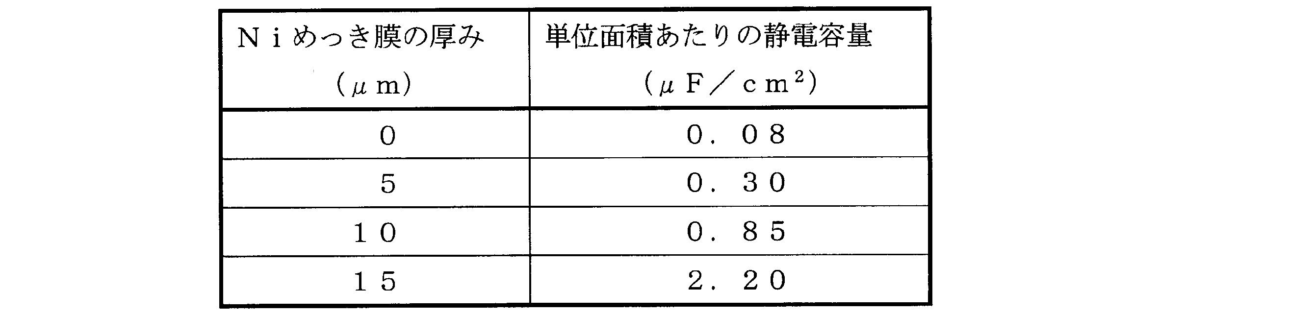
表2からわかるように、Niめっき膜の厚みの増加に従い、単位面積あたりの静電容量が大きく上昇する結果となった。よって、この実施例1による多孔質状のめっき膜の場合、膜厚が増して3次元構造が広がると、実際の比表面積がBET測定値よりも大きくなっていることが考えられる。
実施例2は、実施例1とは異なるNi浴を用いて得られたワイヤ状Niめっき膜を導電性基材としたときのコンデンサを評価したものである。
<前処理>
実施例1と同様に、厚さ10μmのCu箔を用意し、この上に、Pd微粒子を付与した。
実施例1と同様に、厚さ10μmのCu箔を用意し、この上に、Pd微粒子を付与した。
<導電性基材の形成>
以下の表3に示す無電解Niめっき液およびめっき条件により、上記Cu箔上に、導電性基材となる厚み5μmの無電解Niめっき膜を形成した。また、比較例として、無電解Niめっき膜を形成しない試料も残した。
以下の表3に示す無電解Niめっき液およびめっき条件により、上記Cu箔上に、導電性基材となる厚み5μmの無電解Niめっき膜を形成した。また、比較例として、無電解Niめっき膜を形成しない試料も残した。

得られた無電解Niめっき膜の表面をSEM(走査型電子顕微鏡)にて観察した。その結果、めっき膜の形態はワイヤ状であることが確認された。この無電解Niめっき膜について、その表面を撮影したSEM写真が図4に示されている。
<誘電体膜の形成>
次に、上記無電解Niめっき膜の表面に、CVD法によりTiO2からなる誘電体膜を形成した。このTiO2からなる誘電体膜の厚みは約100nmであった。
次に、上記無電解Niめっき膜の表面に、CVD法によりTiO2からなる誘電体膜を形成した。このTiO2からなる誘電体膜の厚みは約100nmであった。
なお、上記比較例では、Cu箔上に、直接、CVD法によりTiO2からなる誘電体膜を形成した。
<対向導電体の形成>
次に、実施例1と同様にして、対向導体膜を形成し、次いで、第2の取出し電極となるアルミニウム箔を配置し、各試料となるコンデンサを完成させた。
次に、実施例1と同様にして、対向導体膜を形成し、次いで、第2の取出し電極となるアルミニウム箔を配置し、各試料となるコンデンサを完成させた。
<評価および考察>
導電性基材となる無電解Niめっき膜を形成した試料について、無電解Niめっき膜の、BET法による体積あたりの比表面積(S/V)は、23400mm2/mm3であった。また、実施例1と同様にして求めた単位面積あたりの静電容量は、310μF/cm2であった。なお、比較例では、0.3μF/cm2であった。
導電性基材となる無電解Niめっき膜を形成した試料について、無電解Niめっき膜の、BET法による体積あたりの比表面積(S/V)は、23400mm2/mm3であった。また、実施例1と同様にして求めた単位面積あたりの静電容量は、310μF/cm2であった。なお、比較例では、0.3μF/cm2であった。
実施例2のように、導電性基材にワイヤ状のNiめっき膜を用いることにより、実施例1よりも大きな比表面積を有する導電性基材を得ることができ、大容量のコンデンサを得ることができた。
実施例3は、実施例1および2のいずれとも異なるNi浴を用いて得られたブロッコリ状Niめっき膜を導電性基材としたときのコンデンサを評価したものである。
<前処理>
実施例1と同様に、厚さ10μmのCu箔を用意し、この上に、Pd微粒子を付与した。
実施例1と同様に、厚さ10μmのCu箔を用意し、この上に、Pd微粒子を付与した。
<導電性基材の形成>
以下の表4に示す無電解Niめっき液およびめっき条件により、上記Cu箔上に、導電性基材となる厚み5μmの無電解Niめっき膜を形成した。
以下の表4に示す無電解Niめっき液およびめっき条件により、上記Cu箔上に、導電性基材となる厚み5μmの無電解Niめっき膜を形成した。

得られた無電解Niめっき膜の表面をSEM(走査型電子顕微鏡)にて観察した。その結果、めっき膜の形態はブロッコリ状であることが確認された。この無電解Niめっき膜について、その表面を撮影したSEM写真が図5に示されている。
<誘電体膜の形成>
次に、上記無電解Niめっき膜の表面に、CVD法によりTiO2からなる誘電体膜を形成した。このTiO2からなる誘電体膜の厚みは約100nmであった。
次に、上記無電解Niめっき膜の表面に、CVD法によりTiO2からなる誘電体膜を形成した。このTiO2からなる誘電体膜の厚みは約100nmであった。
<対向導電体の形成>
次に、実施例1と同様にして、対向導体膜を形成し、次いで、第2の取出し電極となるアルミニウム箔を配置し、各試料となるコンデンサを完成させた。
次に、実施例1と同様にして、対向導体膜を形成し、次いで、第2の取出し電極となるアルミニウム箔を配置し、各試料となるコンデンサを完成させた。
<評価および考察>
導電性基材となる無電解Niめっき膜を形成した試料について、無電解Niめっき膜の、BET法による体積あたりの比表面積(S/V)は、72500mm2/mm3であった。また、実施例1と同様にして求めた単位面積あたりの静電容量は、960μF/cm2であった。
導電性基材となる無電解Niめっき膜を形成した試料について、無電解Niめっき膜の、BET法による体積あたりの比表面積(S/V)は、72500mm2/mm3であった。また、実施例1と同様にして求めた単位面積あたりの静電容量は、960μF/cm2であった。
実施例3のように、導電性基材にブロッコリ状のNiめっき膜を用いることにより、実施例1および2のいずれよりも大きな比表面積を有する導電性基材を得ることができ、さらに大容量のコンデンサを得ることができた。
Claims (7)
- 導電性基材と、前記導電性基材の表面に沿うように形成された誘電体膜と、前記誘電体膜を介して前記導電性基材と対向するように形成された対向導電体とを備え、
導電性基材が、100mm2/mm3以上の比表面積を有するめっき膜からなることを特徴とする、コンデンサ。 - 導電性基材が、NiおよびCuの少なくとも一方を主成分とするめっき析出物からなる、請求項1に記載のコンデンサ。
- 前記導電性基材を構成する前記めっき膜の形態が多孔質状である、請求項1または2に記載のコンデンサ。
- 前記導電性基材を構成する前記めっき膜の形態がワイヤ状である、請求項1または2に記載のコンデンサ。
- 前記導電性基材を構成する前記めっき膜の形態がブロッコリ状である、請求項1または2に記載のコンデンサ。
- 電解めっきまたは無電解めっきにより、100mm2/mm3以上の比表面積を有するめっき膜からなる導電性基材を形成する工程と、
前記導電性基材の表面に沿って誘電体膜を形成する工程と、
前記誘電体膜の表面に対向導電体を形成する工程と
を備える、コンデンサの製造方法。 - 前記電解めっきまたは無電解めっきにおいて使用するめっき液には、アセチレン基を有する界面活性剤が含有される、請求項6に記載のコンデンサの製造方法。
Priority Applications (4)
| Application Number | Priority Date | Filing Date | Title |
|---|---|---|---|
| EP09730684.9A EP2261933A4 (en) | 2008-04-08 | 2009-02-09 | Capacitor and method for manufacturing the same |
| JP2010507186A JP5012996B2 (ja) | 2008-04-08 | 2009-02-09 | コンデンサおよびその製造方法 |
| CN2009801109193A CN101981636B (zh) | 2008-04-08 | 2009-02-09 | 电容器及其制造方法 |
| US12/897,161 US20110020603A1 (en) | 2008-04-08 | 2010-10-04 | Capacitor and method for manufacturing the same |
Applications Claiming Priority (2)
| Application Number | Priority Date | Filing Date | Title |
|---|---|---|---|
| JP2008100040 | 2008-04-08 | ||
| JP2008-100040 | 2008-04-08 |
Related Child Applications (1)
| Application Number | Title | Priority Date | Filing Date |
|---|---|---|---|
| US12/897,161 Continuation-In-Part US20110020603A1 (en) | 2008-04-08 | 2010-10-04 | Capacitor and method for manufacturing the same |
Publications (1)
| Publication Number | Publication Date |
|---|---|
| WO2009125620A1 true WO2009125620A1 (ja) | 2009-10-15 |
Family
ID=41161756
Family Applications (1)
| Application Number | Title | Priority Date | Filing Date |
|---|---|---|---|
| PCT/JP2009/052136 WO2009125620A1 (ja) | 2008-04-08 | 2009-02-09 | コンデンサおよびその製造方法 |
Country Status (5)
| Country | Link |
|---|---|
| US (1) | US20110020603A1 (ja) |
| EP (1) | EP2261933A4 (ja) |
| JP (1) | JP5012996B2 (ja) |
| CN (1) | CN101981636B (ja) |
| WO (1) | WO2009125620A1 (ja) |
Cited By (5)
| Publication number | Priority date | Publication date | Assignee | Title |
|---|---|---|---|---|
| WO2012029405A1 (ja) * | 2010-08-31 | 2012-03-08 | 株式会社村田製作所 | 多孔質金属膜、電極、集電体、それを用いた電気化学センサ、蓄電デバイス及び摺動部材並びに多孔質金属膜の製造方法 |
| JP2013014814A (ja) * | 2011-07-06 | 2013-01-24 | Murata Mfg Co Ltd | 金属膜、電気化学センサ、蓄電デバイス及び摺動部材並びに金属膜の製造方法 |
| JP2013014819A (ja) * | 2011-07-06 | 2013-01-24 | Murata Mfg Co Ltd | 多孔質金属膜、電極、集電体、電気化学センサ、蓄電デバイス及び摺動部材並びに多孔質金属膜の製造方法 |
| JP2013023709A (ja) * | 2011-07-19 | 2013-02-04 | Murata Mfg Co Ltd | 多孔質金属膜、電極、集電体、電気化学センサ、蓄電デバイス及び摺動部材並びに多孔質金属膜の製造方法 |
| JP7407484B2 (ja) | 2020-03-11 | 2024-01-04 | スリーディー グラス ソリューションズ,インク | 超高表面積集積コンデンサ |
Families Citing this family (7)
| Publication number | Priority date | Publication date | Assignee | Title |
|---|---|---|---|---|
| US9461567B2 (en) * | 2012-09-11 | 2016-10-04 | Nakanishi Metal Works Co., Ltd. | Drive control device for drive system including vertical carrier machine |
| CN107710362B (zh) * | 2015-07-23 | 2019-10-18 | 株式会社村田制作所 | 电容器 |
| US10249704B2 (en) * | 2015-08-11 | 2019-04-02 | Murata Manufacturing Co., Ltd. | Capacitor |
| JPWO2018051520A1 (ja) * | 2016-09-16 | 2019-07-11 | 日本蓄電器工業株式会社 | 電解コンデンサ用電極部材および電解コンデンサ |
| JP6583220B2 (ja) * | 2016-11-15 | 2019-10-02 | 株式会社村田製作所 | コンデンサ及びコンデンサの製造方法 |
| CN114730666A (zh) * | 2019-11-29 | 2022-07-08 | 松下知识产权经营株式会社 | 电解电容器用阴极箔、电解电容器、及它们的制造方法 |
| WO2021125183A1 (ja) * | 2019-12-17 | 2021-06-24 | 日本ケミコン株式会社 | 固体電解コンデンサ及びその製造方法 |
Citations (3)
| Publication number | Priority date | Publication date | Assignee | Title |
|---|---|---|---|---|
| JPH05301991A (ja) * | 1990-05-18 | 1993-11-16 | Japan Gore Tex Inc | 金属膜を有する多孔質フッ素樹脂材料及びその製造方法 |
| JPH11340091A (ja) | 1998-05-25 | 1999-12-10 | Toyota Central Res & Dev Lab Inc | コンデンサー及びその製造方法 |
| JP2007123820A (ja) * | 2005-09-30 | 2007-05-17 | Nippon Chemicon Corp | 電解コンデンサ |
Family Cites Families (14)
| Publication number | Priority date | Publication date | Assignee | Title |
|---|---|---|---|---|
| US4488941A (en) * | 1982-09-27 | 1984-12-18 | Sprague Electric Company | Electroplating method for producing porous tantalum capacitor electrode |
| US5041196A (en) * | 1989-12-26 | 1991-08-20 | Olin Corporation | Electrochemical method for producing chlorine dioxide solutions |
| US5445739A (en) * | 1991-02-04 | 1995-08-29 | Japan Gore-Tex, Inc. | Composite membrane that includes a separation membrane |
| US5188890A (en) * | 1991-03-15 | 1993-02-23 | Japan Gore-Tex, Inc. | Metallized porous flourinated resin and process therefor |
| WO1999010167A1 (fr) * | 1997-08-27 | 1999-03-04 | Kabushiki Kaisha Toyota Chuo Kenkyusho | Objet enrobe et procede de fabrication de cet objet |
| IL141592A (en) * | 2001-02-22 | 2007-02-11 | Zvi Finkelstein | Electrolytic capacitors and method for making them |
| US6444478B1 (en) * | 1999-08-31 | 2002-09-03 | Micron Technology, Inc. | Dielectric films and methods of forming same |
| JP4626514B2 (ja) * | 2003-02-18 | 2011-02-09 | 日本電気株式会社 | 燃料電池用電極、燃料電池、およびこれらの製造方法 |
| JP4273309B2 (ja) * | 2003-05-14 | 2009-06-03 | 福田金属箔粉工業株式会社 | 低粗面電解銅箔及びその製造方法 |
| JP4240312B2 (ja) * | 2004-11-25 | 2009-03-18 | ソニー株式会社 | 電池 |
| TWI311384B (en) * | 2004-11-25 | 2009-06-21 | Sony Corporatio | Battery and method of manufacturing the same |
| US20060254922A1 (en) * | 2005-03-21 | 2006-11-16 | Science & Technology Corporation @ Unm | Method of depositing films on aluminum alloys and films made by the method |
| JP4591362B2 (ja) * | 2006-01-25 | 2010-12-01 | 株式会社デンソー | 電子装置の製造方法 |
| WO2007116845A1 (ja) * | 2006-03-31 | 2007-10-18 | Nippon Chemi-Con Corporation | 電解コンデンサ用電極材 |
-
2009
- 2009-02-09 CN CN2009801109193A patent/CN101981636B/zh not_active Expired - Fee Related
- 2009-02-09 WO PCT/JP2009/052136 patent/WO2009125620A1/ja active Application Filing
- 2009-02-09 EP EP09730684.9A patent/EP2261933A4/en not_active Withdrawn
- 2009-02-09 JP JP2010507186A patent/JP5012996B2/ja not_active Expired - Fee Related
-
2010
- 2010-10-04 US US12/897,161 patent/US20110020603A1/en not_active Abandoned
Patent Citations (3)
| Publication number | Priority date | Publication date | Assignee | Title |
|---|---|---|---|---|
| JPH05301991A (ja) * | 1990-05-18 | 1993-11-16 | Japan Gore Tex Inc | 金属膜を有する多孔質フッ素樹脂材料及びその製造方法 |
| JPH11340091A (ja) | 1998-05-25 | 1999-12-10 | Toyota Central Res & Dev Lab Inc | コンデンサー及びその製造方法 |
| JP2007123820A (ja) * | 2005-09-30 | 2007-05-17 | Nippon Chemicon Corp | 電解コンデンサ |
Non-Patent Citations (1)
| Title |
|---|
| See also references of EP2261933A4 |
Cited By (6)
| Publication number | Priority date | Publication date | Assignee | Title |
|---|---|---|---|---|
| WO2012029405A1 (ja) * | 2010-08-31 | 2012-03-08 | 株式会社村田製作所 | 多孔質金属膜、電極、集電体、それを用いた電気化学センサ、蓄電デバイス及び摺動部材並びに多孔質金属膜の製造方法 |
| JP5673682B2 (ja) * | 2010-08-31 | 2015-02-18 | 株式会社村田製作所 | 多孔質無電解めっき膜、電極、集電体、それを用いた電気化学センサ、蓄電デバイス及び摺動部材並びに多孔質無電解めっき膜の製造方法 |
| JP2013014814A (ja) * | 2011-07-06 | 2013-01-24 | Murata Mfg Co Ltd | 金属膜、電気化学センサ、蓄電デバイス及び摺動部材並びに金属膜の製造方法 |
| JP2013014819A (ja) * | 2011-07-06 | 2013-01-24 | Murata Mfg Co Ltd | 多孔質金属膜、電極、集電体、電気化学センサ、蓄電デバイス及び摺動部材並びに多孔質金属膜の製造方法 |
| JP2013023709A (ja) * | 2011-07-19 | 2013-02-04 | Murata Mfg Co Ltd | 多孔質金属膜、電極、集電体、電気化学センサ、蓄電デバイス及び摺動部材並びに多孔質金属膜の製造方法 |
| JP7407484B2 (ja) | 2020-03-11 | 2024-01-04 | スリーディー グラス ソリューションズ,インク | 超高表面積集積コンデンサ |
Also Published As
| Publication number | Publication date |
|---|---|
| CN101981636B (zh) | 2013-09-11 |
| CN101981636A (zh) | 2011-02-23 |
| EP2261933A4 (en) | 2018-03-28 |
| JP5012996B2 (ja) | 2012-08-29 |
| EP2261933A1 (en) | 2010-12-15 |
| US20110020603A1 (en) | 2011-01-27 |
| JPWO2009125620A1 (ja) | 2011-08-04 |
Similar Documents
| Publication | Publication Date | Title |
|---|---|---|
| JP5012996B2 (ja) | コンデンサおよびその製造方法 | |
| US20140268490A1 (en) | Super Capacitor And Method For Manufacturing The Same | |
| JP5816794B2 (ja) | 電極箔の製造方法 | |
| US8208242B2 (en) | Electrode foil and capacitor using the same | |
| JP2003272959A (ja) | コンデンサ | |
| JP2015073015A (ja) | 電極箔、電解コンデンサおよび電極箔の製造方法 | |
| JP4553770B2 (ja) | 固体電解コンデンサおよびその製造方法 | |
| JP2015115475A (ja) | 電極箔、電解コンデンサおよび電極箔の製造方法 | |
| JP6432685B2 (ja) | コンデンサ | |
| KR20130076793A (ko) | 전극 구조체의 제조 방법, 전극 구조체 및 콘덴서 | |
| JP4797754B2 (ja) | 電解コンデンサ用電極材 | |
| JP4454526B2 (ja) | 固体電解コンデンサおよびその製造方法 | |
| JP2004524686A (ja) | 電解コンデンサーおよびその作製方法 | |
| US10249704B2 (en) | Capacitor | |
| JP2010098163A (ja) | 固体電解コンデンサ | |
| JP4665854B2 (ja) | バルブ金属複合電極箔およびその製造方法 | |
| JP5493712B2 (ja) | 電極箔とその製造方法およびこの電極箔を用いたコンデンサ | |
| JP2009049376A (ja) | コンデンサ用電極箔 | |
| US20180174760A1 (en) | Capacitor | |
| JP2002367856A (ja) | コンデンサおよびその製造方法 | |
| JP2011249488A (ja) | 電極箔とこの電極箔を用いたコンデンサおよび電極箔の製造方法 | |
| JP6907876B2 (ja) | 成膜方法 | |
| JP4505612B2 (ja) | 金属表面処理方法 | |
| JP2012193420A (ja) | 電極箔の製造方法と電解コンデンサの製造方法、および電極箔と電解コンデンサ | |
| KR20100123606A (ko) | 고체 전해 콘덴서 소자 및 고체 전해 콘덴서 |
Legal Events
| Date | Code | Title | Description |
|---|---|---|---|
| WWE | Wipo information: entry into national phase |
Ref document number: 200980110919.3 Country of ref document: CN |
|
| 121 | Ep: the epo has been informed by wipo that ep was designated in this application |
Ref document number: 09730684 Country of ref document: EP Kind code of ref document: A1 |
|
| WWE | Wipo information: entry into national phase |
Ref document number: 2010507186 Country of ref document: JP |
|
| WWE | Wipo information: entry into national phase |
Ref document number: 2009730684 Country of ref document: EP |
|
| NENP | Non-entry into the national phase |
Ref country code: DE |