WO2009102004A1 - 洗浄剤組成物および電子デバイス用基板の洗浄方法 - Google Patents
洗浄剤組成物および電子デバイス用基板の洗浄方法 Download PDFInfo
- Publication number
- WO2009102004A1 WO2009102004A1 PCT/JP2009/052383 JP2009052383W WO2009102004A1 WO 2009102004 A1 WO2009102004 A1 WO 2009102004A1 JP 2009052383 W JP2009052383 W JP 2009052383W WO 2009102004 A1 WO2009102004 A1 WO 2009102004A1
- Authority
- WO
- WIPO (PCT)
- Prior art keywords
- cleaning
- substrate
- cleaning composition
- electronic device
- component
- Prior art date
Links
- 238000004140 cleaning Methods 0.000 title claims abstract description 227
- 239000000758 substrate Substances 0.000 title claims abstract description 186
- 239000000203 mixture Substances 0.000 title claims abstract description 138
- 238000000034 method Methods 0.000 title claims abstract description 65
- 239000002738 chelating agent Substances 0.000 claims abstract description 24
- 150000003839 salts Chemical class 0.000 claims abstract description 23
- 229910052723 transition metal Inorganic materials 0.000 claims abstract description 19
- 150000003624 transition metals Chemical class 0.000 claims abstract description 19
- 150000002978 peroxides Chemical class 0.000 claims abstract description 13
- 239000002253 acid Substances 0.000 claims description 31
- HBMJWWWQQXIZIP-UHFFFAOYSA-N silicon carbide Chemical compound [Si+]#[C-] HBMJWWWQQXIZIP-UHFFFAOYSA-N 0.000 claims description 30
- PXHVJJICTQNCMI-UHFFFAOYSA-N Nickel Chemical compound [Ni] PXHVJJICTQNCMI-UHFFFAOYSA-N 0.000 claims description 22
- 229910010271 silicon carbide Inorganic materials 0.000 claims description 17
- 239000004065 semiconductor Substances 0.000 claims description 15
- XEEYBQQBJWHFJM-UHFFFAOYSA-N Iron Chemical compound [Fe] XEEYBQQBJWHFJM-UHFFFAOYSA-N 0.000 claims description 14
- 229910052759 nickel Inorganic materials 0.000 claims description 11
- 239000000463 material Substances 0.000 claims description 10
- 150000001875 compounds Chemical class 0.000 claims description 9
- XLOMVQKBTHCTTD-UHFFFAOYSA-N Zinc monoxide Chemical compound [Zn]=O XLOMVQKBTHCTTD-UHFFFAOYSA-N 0.000 claims description 8
- 239000011521 glass Substances 0.000 claims description 8
- 229910052742 iron Inorganic materials 0.000 claims description 8
- 238000009210 therapy by ultrasound Methods 0.000 claims description 8
- XUIMIQQOPSSXEZ-UHFFFAOYSA-N Silicon Chemical compound [Si] XUIMIQQOPSSXEZ-UHFFFAOYSA-N 0.000 claims description 6
- 229910052710 silicon Inorganic materials 0.000 claims description 6
- 239000010703 silicon Substances 0.000 claims description 6
- OAICVXFJPJFONN-UHFFFAOYSA-N Phosphorus Chemical compound [P] OAICVXFJPJFONN-UHFFFAOYSA-N 0.000 claims description 5
- 229910052698 phosphorus Inorganic materials 0.000 claims description 5
- 239000011574 phosphorus Substances 0.000 claims description 5
- 229910052782 aluminium Inorganic materials 0.000 claims description 4
- XAGFODPZIPBFFR-UHFFFAOYSA-N aluminium Chemical compound [Al] XAGFODPZIPBFFR-UHFFFAOYSA-N 0.000 claims description 4
- 229910052594 sapphire Inorganic materials 0.000 claims description 4
- 239000010980 sapphire Substances 0.000 claims description 4
- 239000011787 zinc oxide Substances 0.000 claims description 4
- 239000002245 particle Substances 0.000 abstract description 50
- 230000007613 environmental effect Effects 0.000 abstract description 3
- 238000011086 high cleaning Methods 0.000 abstract 1
- 230000003749 cleanliness Effects 0.000 description 47
- 238000011156 evaluation Methods 0.000 description 46
- MHAJPDPJQMAIIY-UHFFFAOYSA-N Hydrogen peroxide Chemical compound OO MHAJPDPJQMAIIY-UHFFFAOYSA-N 0.000 description 35
- RYGMFSIKBFXOCR-UHFFFAOYSA-N Copper Chemical compound [Cu] RYGMFSIKBFXOCR-UHFFFAOYSA-N 0.000 description 30
- 229910021642 ultra pure water Inorganic materials 0.000 description 26
- 239000012498 ultrapure water Substances 0.000 description 26
- 239000000126 substance Substances 0.000 description 25
- 229910052751 metal Inorganic materials 0.000 description 23
- 239000002184 metal Substances 0.000 description 23
- 238000002360 preparation method Methods 0.000 description 23
- KRHYYFGTRYWZRS-UHFFFAOYSA-N Fluorane Chemical compound F KRHYYFGTRYWZRS-UHFFFAOYSA-N 0.000 description 20
- 238000002156 mixing Methods 0.000 description 18
- 229960002163 hydrogen peroxide Drugs 0.000 description 17
- 239000007864 aqueous solution Substances 0.000 description 15
- 239000003513 alkali Substances 0.000 description 14
- 239000000356 contaminant Substances 0.000 description 14
- 230000008569 process Effects 0.000 description 14
- VYPSYNLAJGMNEJ-UHFFFAOYSA-N Silicium dioxide Chemical compound O=[Si]=O VYPSYNLAJGMNEJ-UHFFFAOYSA-N 0.000 description 12
- HEMHJVSKTPXQMS-UHFFFAOYSA-M Sodium hydroxide Chemical compound [OH-].[Na+] HEMHJVSKTPXQMS-UHFFFAOYSA-M 0.000 description 12
- XLYOFNOQVPJJNP-UHFFFAOYSA-N water Substances O XLYOFNOQVPJJNP-UHFFFAOYSA-N 0.000 description 11
- 150000004696 coordination complex Chemical class 0.000 description 10
- 238000005498 polishing Methods 0.000 description 10
- WGTYBPLFGIVFAS-UHFFFAOYSA-M tetramethylammonium hydroxide Chemical compound [OH-].C[N+](C)(C)C WGTYBPLFGIVFAS-UHFFFAOYSA-M 0.000 description 10
- KFZMGEQAYNKOFK-UHFFFAOYSA-N Isopropanol Chemical compound CC(C)O KFZMGEQAYNKOFK-UHFFFAOYSA-N 0.000 description 9
- KWYUFKZDYYNOTN-UHFFFAOYSA-M Potassium hydroxide Chemical compound [OH-].[K+] KWYUFKZDYYNOTN-UHFFFAOYSA-M 0.000 description 9
- 239000003795 chemical substances by application Substances 0.000 description 9
- 238000011109 contamination Methods 0.000 description 9
- 229940073644 nickel Drugs 0.000 description 9
- 238000004506 ultrasonic cleaning Methods 0.000 description 9
- 238000005406 washing Methods 0.000 description 9
- -1 and the like Chemical class 0.000 description 8
- 239000003599 detergent Substances 0.000 description 8
- 239000005416 organic matter Substances 0.000 description 8
- 238000012360 testing method Methods 0.000 description 8
- OBMBUODDCOAJQP-UHFFFAOYSA-N 2-chloro-4-phenylquinoline Chemical compound C=12C=CC=CC2=NC(Cl)=CC=1C1=CC=CC=C1 OBMBUODDCOAJQP-UHFFFAOYSA-N 0.000 description 7
- 238000007654 immersion Methods 0.000 description 7
- 239000010453 quartz Substances 0.000 description 7
- VEXZGXHMUGYJMC-UHFFFAOYSA-N Hydrochloric acid Chemical compound Cl VEXZGXHMUGYJMC-UHFFFAOYSA-N 0.000 description 6
- QAOWNCQODCNURD-UHFFFAOYSA-N Sulfuric acid Chemical compound OS(O)(=O)=O QAOWNCQODCNURD-UHFFFAOYSA-N 0.000 description 6
- 239000002689 soil Substances 0.000 description 6
- 238000007796 conventional method Methods 0.000 description 5
- 239000010949 copper Substances 0.000 description 5
- 238000000354 decomposition reaction Methods 0.000 description 5
- 230000000694 effects Effects 0.000 description 5
- 230000010355 oscillation Effects 0.000 description 5
- 239000000523 sample Substances 0.000 description 5
- 239000011550 stock solution Substances 0.000 description 5
- 231100000331 toxic Toxicity 0.000 description 5
- 230000002588 toxic effect Effects 0.000 description 5
- QGZKDVFQNNGYKY-UHFFFAOYSA-N Ammonia Chemical compound N QGZKDVFQNNGYKY-UHFFFAOYSA-N 0.000 description 4
- IJGRMHOSHXDMSA-UHFFFAOYSA-N Atomic nitrogen Chemical compound N#N IJGRMHOSHXDMSA-UHFFFAOYSA-N 0.000 description 4
- LFQSCWFLJHTTHZ-UHFFFAOYSA-N Ethanol Chemical compound CCO LFQSCWFLJHTTHZ-UHFFFAOYSA-N 0.000 description 4
- 229910052802 copper Inorganic materials 0.000 description 4
- 159000000000 sodium salts Chemical class 0.000 description 4
- 239000002904 solvent Substances 0.000 description 4
- JSYPRLVDJYQMAI-ODZAUARKSA-N (z)-but-2-enedioic acid;prop-2-enoic acid Chemical compound OC(=O)C=C.OC(=O)\C=C/C(O)=O JSYPRLVDJYQMAI-ODZAUARKSA-N 0.000 description 3
- 229920002126 Acrylic acid copolymer Polymers 0.000 description 3
- 229920002873 Polyethylenimine Polymers 0.000 description 3
- 150000001805 chlorine compounds Chemical class 0.000 description 3
- 239000012459 cleaning agent Substances 0.000 description 3
- 229910017052 cobalt Inorganic materials 0.000 description 3
- 239000010941 cobalt Substances 0.000 description 3
- GUTLYIVDDKVIGB-UHFFFAOYSA-N cobalt atom Chemical compound [Co] GUTLYIVDDKVIGB-UHFFFAOYSA-N 0.000 description 3
- 239000008119 colloidal silica Substances 0.000 description 3
- 230000000052 comparative effect Effects 0.000 description 3
- XTVVROIMIGLXTD-UHFFFAOYSA-N copper(II) nitrate Chemical compound [Cu+2].[O-][N+]([O-])=O.[O-][N+]([O-])=O XTVVROIMIGLXTD-UHFFFAOYSA-N 0.000 description 3
- RTZKZFJDLAIYFH-UHFFFAOYSA-N ether Substances CCOCC RTZKZFJDLAIYFH-UHFFFAOYSA-N 0.000 description 3
- 229920002313 fluoropolymer Polymers 0.000 description 3
- 239000004811 fluoropolymer Substances 0.000 description 3
- 238000005187 foaming Methods 0.000 description 3
- 150000002823 nitrates Chemical class 0.000 description 3
- MGFYIUFZLHCRTH-UHFFFAOYSA-N nitrilotriacetic acid Chemical compound OC(=O)CN(CC(O)=O)CC(O)=O MGFYIUFZLHCRTH-UHFFFAOYSA-N 0.000 description 3
- 238000001139 pH measurement Methods 0.000 description 3
- 238000007517 polishing process Methods 0.000 description 3
- XAEFZNCEHLXOMS-UHFFFAOYSA-M potassium benzoate Chemical compound [K+].[O-]C(=O)C1=CC=CC=C1 XAEFZNCEHLXOMS-UHFFFAOYSA-M 0.000 description 3
- 150000003467 sulfuric acid derivatives Chemical class 0.000 description 3
- 239000004094 surface-active agent Substances 0.000 description 3
- DCCWEYXHEXDZQW-BYPYZUCNSA-N (2s)-2-[bis(carboxymethyl)amino]butanedioic acid Chemical compound OC(=O)C[C@@H](C(O)=O)N(CC(O)=O)CC(O)=O DCCWEYXHEXDZQW-BYPYZUCNSA-N 0.000 description 2
- CFPOJWPDQWJEMO-UHFFFAOYSA-N 2-(1,2-dicarboxyethoxy)butanedioic acid Chemical compound OC(=O)CC(C(O)=O)OC(C(O)=O)CC(O)=O CFPOJWPDQWJEMO-UHFFFAOYSA-N 0.000 description 2
- PQHYOGIRXOKOEJ-UHFFFAOYSA-N 2-(1,2-dicarboxyethylamino)butanedioic acid Chemical compound OC(=O)CC(C(O)=O)NC(C(O)=O)CC(O)=O PQHYOGIRXOKOEJ-UHFFFAOYSA-N 0.000 description 2
- JPGSFSFMINKKJZ-UHFFFAOYSA-N 2-[1,2-dicarboxyethyl(hydroxy)amino]butanedioic acid Chemical compound OC(=O)CC(C(O)=O)N(O)C(CC(O)=O)C(O)=O JPGSFSFMINKKJZ-UHFFFAOYSA-N 0.000 description 2
- UWRBFYBQPCJRRL-UHFFFAOYSA-N 3-[bis(carboxymethyl)amino]propanoic acid Chemical compound OC(=O)CCN(CC(O)=O)CC(O)=O UWRBFYBQPCJRRL-UHFFFAOYSA-N 0.000 description 2
- KCXVZYZYPLLWCC-UHFFFAOYSA-N EDTA Chemical compound OC(=O)CN(CC(O)=O)CCN(CC(O)=O)CC(O)=O KCXVZYZYPLLWCC-UHFFFAOYSA-N 0.000 description 2
- WHUUTDBJXJRKMK-VKHMYHEASA-N L-glutamic acid Chemical compound OC(=O)[C@@H](N)CCC(O)=O WHUUTDBJXJRKMK-VKHMYHEASA-N 0.000 description 2
- GRYLNZFGIOXLOG-UHFFFAOYSA-N Nitric acid Chemical compound O[N+]([O-])=O GRYLNZFGIOXLOG-UHFFFAOYSA-N 0.000 description 2
- CBENFWSGALASAD-UHFFFAOYSA-N Ozone Chemical compound [O-][O+]=O CBENFWSGALASAD-UHFFFAOYSA-N 0.000 description 2
- MTCFGRXMJLQNBG-UHFFFAOYSA-N Serine Natural products OCC(N)C(O)=O MTCFGRXMJLQNBG-UHFFFAOYSA-N 0.000 description 2
- BQCADISMDOOEFD-UHFFFAOYSA-N Silver Chemical compound [Ag] BQCADISMDOOEFD-UHFFFAOYSA-N 0.000 description 2
- PDIZYYQQWUOPPK-UHFFFAOYSA-N acetic acid;2-(methylamino)acetic acid Chemical compound CC(O)=O.CC(O)=O.CNCC(O)=O PDIZYYQQWUOPPK-UHFFFAOYSA-N 0.000 description 2
- 150000007513 acids Chemical class 0.000 description 2
- 229910052783 alkali metal Inorganic materials 0.000 description 2
- 229910021529 ammonia Inorganic materials 0.000 description 2
- SXDBWCPKPHAZSM-UHFFFAOYSA-M bromate Chemical class [O-]Br(=O)=O SXDBWCPKPHAZSM-UHFFFAOYSA-M 0.000 description 2
- HXDRSFFFXJISME-UHFFFAOYSA-N butanedioic acid;2,3-dihydroxybutanedioic acid Chemical compound OC(=O)CCC(O)=O.OC(=O)C(O)C(O)C(O)=O HXDRSFFFXJISME-UHFFFAOYSA-N 0.000 description 2
- 238000011088 calibration curve Methods 0.000 description 2
- 238000013329 compounding Methods 0.000 description 2
- 238000005260 corrosion Methods 0.000 description 2
- 230000007797 corrosion Effects 0.000 description 2
- STZIXLPVKZUAMV-UHFFFAOYSA-N cyclopentane-1,1,2,2-tetracarboxylic acid Chemical class OC(=O)C1(C(O)=O)CCCC1(C(O)=O)C(O)=O STZIXLPVKZUAMV-UHFFFAOYSA-N 0.000 description 2
- 238000010790 dilution Methods 0.000 description 2
- 239000012895 dilution Substances 0.000 description 2
- 238000001035 drying Methods 0.000 description 2
- 229940071106 ethylenediaminetetraacetate Drugs 0.000 description 2
- 229940049906 glutamate Drugs 0.000 description 2
- 229930195712 glutamate Natural products 0.000 description 2
- 229940080260 iminodisuccinate Drugs 0.000 description 2
- 239000004615 ingredient Substances 0.000 description 2
- WPBNNNQJVZRUHP-UHFFFAOYSA-L manganese(2+);methyl n-[[2-(methoxycarbonylcarbamothioylamino)phenyl]carbamothioyl]carbamate;n-[2-(sulfidocarbothioylamino)ethyl]carbamodithioate Chemical compound [Mn+2].[S-]C(=S)NCCNC([S-])=S.COC(=O)NC(=S)NC1=CC=CC=C1NC(=S)NC(=O)OC WPBNNNQJVZRUHP-UHFFFAOYSA-L 0.000 description 2
- 238000005259 measurement Methods 0.000 description 2
- 229910021645 metal ion Inorganic materials 0.000 description 2
- 150000007522 mineralic acids Chemical class 0.000 description 2
- 229910017604 nitric acid Inorganic materials 0.000 description 2
- 229910052757 nitrogen Inorganic materials 0.000 description 2
- 230000001590 oxidative effect Effects 0.000 description 2
- QPCDCPDFJACHGM-UHFFFAOYSA-K pentetate(3-) Chemical compound OC(=O)CN(CC([O-])=O)CCN(CC([O-])=O)CCN(CC(O)=O)CC([O-])=O QPCDCPDFJACHGM-UHFFFAOYSA-K 0.000 description 2
- 229920000642 polymer Polymers 0.000 description 2
- CYIDZMCFTVVTJO-UHFFFAOYSA-N pyromellitic acid Chemical class OC(=O)C1=CC(C(O)=O)=C(C(O)=O)C=C1C(O)=O CYIDZMCFTVVTJO-UHFFFAOYSA-N 0.000 description 2
- 238000011002 quantification Methods 0.000 description 2
- 229910052709 silver Inorganic materials 0.000 description 2
- 239000004332 silver Substances 0.000 description 2
- YPNVIBVEFVRZPJ-UHFFFAOYSA-L silver sulfate Chemical compound [Ag+].[Ag+].[O-]S([O-])(=O)=O YPNVIBVEFVRZPJ-UHFFFAOYSA-L 0.000 description 2
- 229910000367 silver sulfate Inorganic materials 0.000 description 2
- SQGYOTSLMSWVJD-UHFFFAOYSA-N silver(1+) nitrate Chemical compound [Ag+].[O-]N(=O)=O SQGYOTSLMSWVJD-UHFFFAOYSA-N 0.000 description 2
- 229910052708 sodium Inorganic materials 0.000 description 2
- 239000011734 sodium Substances 0.000 description 2
- 235000019832 sodium triphosphate Nutrition 0.000 description 2
- 239000000243 solution Substances 0.000 description 2
- CIOXZGOUEYHNBF-UHFFFAOYSA-N (carboxymethoxy)succinic acid Chemical compound OC(=O)COC(C(O)=O)CC(O)=O CIOXZGOUEYHNBF-UHFFFAOYSA-N 0.000 description 1
- OVSKIKFHRZPJSS-UHFFFAOYSA-N 2,4-D Chemical compound OC(=O)COC1=CC=C(Cl)C=C1Cl OVSKIKFHRZPJSS-UHFFFAOYSA-N 0.000 description 1
- QTBSBXVTEAMEQO-UHFFFAOYSA-M Acetate Chemical compound CC([O-])=O QTBSBXVTEAMEQO-UHFFFAOYSA-M 0.000 description 1
- JBRZTFJDHDCESZ-UHFFFAOYSA-N AsGa Chemical compound [As]#[Ga] JBRZTFJDHDCESZ-UHFFFAOYSA-N 0.000 description 1
- 229910052580 B4C Inorganic materials 0.000 description 1
- KXDHJXZQYSOELW-UHFFFAOYSA-N Carbamic acid Chemical class NC(O)=O KXDHJXZQYSOELW-UHFFFAOYSA-N 0.000 description 1
- OKTJSMMVPCPJKN-UHFFFAOYSA-N Carbon Chemical compound [C] OKTJSMMVPCPJKN-UHFFFAOYSA-N 0.000 description 1
- KRKNYBCHXYNGOX-UHFFFAOYSA-K Citrate Chemical compound [O-]C(=O)CC(O)(CC([O-])=O)C([O-])=O KRKNYBCHXYNGOX-UHFFFAOYSA-K 0.000 description 1
- OCUCCJIRFHNWBP-IYEMJOQQSA-L Copper gluconate Chemical class [Cu+2].OC[C@@H](O)[C@@H](O)[C@H](O)[C@@H](O)C([O-])=O.OC[C@@H](O)[C@@H](O)[C@H](O)[C@@H](O)C([O-])=O OCUCCJIRFHNWBP-IYEMJOQQSA-L 0.000 description 1
- FEWJPZIEWOKRBE-JCYAYHJZSA-N Dextrotartaric acid Chemical compound OC(=O)[C@H](O)[C@@H](O)C(O)=O FEWJPZIEWOKRBE-JCYAYHJZSA-N 0.000 description 1
- DBVJJBKOTRCVKF-UHFFFAOYSA-N Etidronic acid Chemical compound OP(=O)(O)C(O)(C)P(O)(O)=O DBVJJBKOTRCVKF-UHFFFAOYSA-N 0.000 description 1
- 229910002601 GaN Inorganic materials 0.000 description 1
- 229910001218 Gallium arsenide Inorganic materials 0.000 description 1
- JMASRVWKEDWRBT-UHFFFAOYSA-N Gallium nitride Chemical compound [Ga]#N JMASRVWKEDWRBT-UHFFFAOYSA-N 0.000 description 1
- DRAJWRKLRBNJRQ-UHFFFAOYSA-N Hydroxycarbamic acid Chemical class ONC(O)=O DRAJWRKLRBNJRQ-UHFFFAOYSA-N 0.000 description 1
- 208000018208 Hyperimmunoglobulinemia D with periodic fever Diseases 0.000 description 1
- GPXJNWSHGFTCBW-UHFFFAOYSA-N Indium phosphide Chemical compound [In]#P GPXJNWSHGFTCBW-UHFFFAOYSA-N 0.000 description 1
- 229910021380 Manganese Chloride Inorganic materials 0.000 description 1
- GLFNIEUTAYBVOC-UHFFFAOYSA-L Manganese chloride Chemical compound Cl[Mn]Cl GLFNIEUTAYBVOC-UHFFFAOYSA-L 0.000 description 1
- 206010072219 Mevalonic aciduria Diseases 0.000 description 1
- FSVCELGFZIQNCK-UHFFFAOYSA-N N,N-bis(2-hydroxyethyl)glycine Chemical compound OCCN(CCO)CC(O)=O FSVCELGFZIQNCK-UHFFFAOYSA-N 0.000 description 1
- 229910021585 Nickel(II) bromide Inorganic materials 0.000 description 1
- 229910021586 Nickel(II) chloride Inorganic materials 0.000 description 1
- 229920000297 Rayon Polymers 0.000 description 1
- VMHLLURERBWHNL-UHFFFAOYSA-M Sodium acetate Chemical compound [Na+].CC([O-])=O VMHLLURERBWHNL-UHFFFAOYSA-M 0.000 description 1
- 229910000831 Steel Inorganic materials 0.000 description 1
- YZCLSZPQXZWSCJ-UHFFFAOYSA-L [Na+].[Na+].CCO.[O-]P(=O)OP([O-])=O Chemical compound [Na+].[Na+].CCO.[O-]P(=O)OP([O-])=O YZCLSZPQXZWSCJ-UHFFFAOYSA-L 0.000 description 1
- 239000003082 abrasive agent Substances 0.000 description 1
- 238000002835 absorbance Methods 0.000 description 1
- JTPLPDIKCDKODU-UHFFFAOYSA-N acetic acid;2-(2-aminoethylamino)ethanol Chemical compound CC(O)=O.CC(O)=O.CC(O)=O.NCCNCCO JTPLPDIKCDKODU-UHFFFAOYSA-N 0.000 description 1
- 239000012190 activator Substances 0.000 description 1
- 150000001298 alcohols Chemical class 0.000 description 1
- 150000008051 alkyl sulfates Chemical class 0.000 description 1
- 125000002947 alkylene group Chemical group 0.000 description 1
- 150000003863 ammonium salts Chemical class 0.000 description 1
- 239000003945 anionic surfactant Substances 0.000 description 1
- 230000008901 benefit Effects 0.000 description 1
- 238000007664 blowing Methods 0.000 description 1
- KGBXLFKZBHKPEV-UHFFFAOYSA-N boric acid Chemical compound OB(O)O KGBXLFKZBHKPEV-UHFFFAOYSA-N 0.000 description 1
- 239000004327 boric acid Substances 0.000 description 1
- INAHAJYZKVIDIZ-UHFFFAOYSA-N boron carbide Chemical compound B12B3B4C32B41 INAHAJYZKVIDIZ-UHFFFAOYSA-N 0.000 description 1
- ODWXUNBKCRECNW-UHFFFAOYSA-M bromocopper(1+) Chemical compound Br[Cu+] ODWXUNBKCRECNW-UHFFFAOYSA-M 0.000 description 1
- CMFFZBGFNICZIS-UHFFFAOYSA-N butanedioic acid;2,3-dihydroxybutanedioic acid Chemical compound OC(=O)CCC(O)=O.OC(=O)CCC(O)=O.OC(=O)C(O)C(O)C(O)=O CMFFZBGFNICZIS-UHFFFAOYSA-N 0.000 description 1
- LLSDKQJKOVVTOJ-UHFFFAOYSA-L calcium chloride dihydrate Chemical compound O.O.[Cl-].[Cl-].[Ca+2] LLSDKQJKOVVTOJ-UHFFFAOYSA-L 0.000 description 1
- 229940052299 calcium chloride dihydrate Drugs 0.000 description 1
- 229910052799 carbon Inorganic materials 0.000 description 1
- RBNGONPWBVARIG-UHFFFAOYSA-N carbonic acid;2-hydroxyacetic acid Chemical class OC(O)=O.OCC(O)=O RBNGONPWBVARIG-UHFFFAOYSA-N 0.000 description 1
- 238000003763 carbonization Methods 0.000 description 1
- 230000015556 catabolic process Effects 0.000 description 1
- 238000006243 chemical reaction Methods 0.000 description 1
- 150000001860 citric acid derivatives Chemical class 0.000 description 1
- GVPFVAHMJGGAJG-UHFFFAOYSA-L cobalt dichloride Chemical compound [Cl-].[Cl-].[Co+2] GVPFVAHMJGGAJG-UHFFFAOYSA-L 0.000 description 1
- UFMZWBIQTDUYBN-UHFFFAOYSA-N cobalt dinitrate Chemical compound [Co+2].[O-][N+]([O-])=O.[O-][N+]([O-])=O UFMZWBIQTDUYBN-UHFFFAOYSA-N 0.000 description 1
- 229910001981 cobalt nitrate Inorganic materials 0.000 description 1
- 229910000361 cobalt sulfate Inorganic materials 0.000 description 1
- 229940044175 cobalt sulfate Drugs 0.000 description 1
- KTVIXTQDYHMGHF-UHFFFAOYSA-L cobalt(2+) sulfate Chemical compound [Co+2].[O-]S([O-])(=O)=O KTVIXTQDYHMGHF-UHFFFAOYSA-L 0.000 description 1
- MEYVLGVRTYSQHI-UHFFFAOYSA-L cobalt(2+) sulfate heptahydrate Chemical compound O.O.O.O.O.O.O.[Co+2].[O-]S([O-])(=O)=O MEYVLGVRTYSQHI-UHFFFAOYSA-L 0.000 description 1
- BZRRQSJJPUGBAA-UHFFFAOYSA-L cobalt(ii) bromide Chemical compound Br[Co]Br BZRRQSJJPUGBAA-UHFFFAOYSA-L 0.000 description 1
- 229910000365 copper sulfate Inorganic materials 0.000 description 1
- ORTQZVOHEJQUHG-UHFFFAOYSA-L copper(II) chloride Chemical compound Cl[Cu]Cl ORTQZVOHEJQUHG-UHFFFAOYSA-L 0.000 description 1
- MPTQRFCYZCXJFQ-UHFFFAOYSA-L copper(II) chloride dihydrate Chemical compound O.O.[Cl-].[Cl-].[Cu+2] MPTQRFCYZCXJFQ-UHFFFAOYSA-L 0.000 description 1
- ARUVKPQLZAKDPS-UHFFFAOYSA-L copper(II) sulfate Chemical compound [Cu+2].[O-][S+2]([O-])([O-])[O-] ARUVKPQLZAKDPS-UHFFFAOYSA-L 0.000 description 1
- JZCCFEFSEZPSOG-UHFFFAOYSA-L copper(II) sulfate pentahydrate Chemical compound O.O.O.O.O.[Cu+2].[O-]S([O-])(=O)=O JZCCFEFSEZPSOG-UHFFFAOYSA-L 0.000 description 1
- 230000009849 deactivation Effects 0.000 description 1
- 238000006731 degradation reaction Methods 0.000 description 1
- 229910003460 diamond Inorganic materials 0.000 description 1
- 239000010432 diamond Substances 0.000 description 1
- RJYMRRJVDRJMJW-UHFFFAOYSA-L dibromomanganese Chemical compound Br[Mn]Br RJYMRRJVDRJMJW-UHFFFAOYSA-L 0.000 description 1
- ZBCBWPMODOFKDW-UHFFFAOYSA-N diethanolamine Chemical class OCCNCCO ZBCBWPMODOFKDW-UHFFFAOYSA-N 0.000 description 1
- XPPKVPWEQAFLFU-UHFFFAOYSA-N diphosphoric acid Chemical compound OP(O)(=O)OP(O)(O)=O XPPKVPWEQAFLFU-UHFFFAOYSA-N 0.000 description 1
- VTIIJXUACCWYHX-UHFFFAOYSA-L disodium;carboxylatooxy carbonate Chemical compound [Na+].[Na+].[O-]C(=O)OOC([O-])=O VTIIJXUACCWYHX-UHFFFAOYSA-L 0.000 description 1
- 150000002169 ethanolamines Chemical class 0.000 description 1
- 229960004585 etidronic acid Drugs 0.000 description 1
- NBVXSUQYWXRMNV-UHFFFAOYSA-N fluoromethane Chemical compound FC NBVXSUQYWXRMNV-UHFFFAOYSA-N 0.000 description 1
- 230000003993 interaction Effects 0.000 description 1
- FBAFATDZDUQKNH-UHFFFAOYSA-M iron chloride Chemical compound [Cl-].[Fe] FBAFATDZDUQKNH-UHFFFAOYSA-M 0.000 description 1
- 229910000358 iron sulfate Inorganic materials 0.000 description 1
- BAUYGSIQEAFULO-UHFFFAOYSA-L iron(2+) sulfate (anhydrous) Chemical compound [Fe+2].[O-]S([O-])(=O)=O BAUYGSIQEAFULO-UHFFFAOYSA-L 0.000 description 1
- SURQXAFEQWPFPV-UHFFFAOYSA-L iron(2+) sulfate heptahydrate Chemical compound O.O.O.O.O.O.O.[Fe+2].[O-]S([O-])(=O)=O SURQXAFEQWPFPV-UHFFFAOYSA-L 0.000 description 1
- MVFCKEFYUDZOCX-UHFFFAOYSA-N iron(2+);dinitrate Chemical compound [Fe+2].[O-][N+]([O-])=O.[O-][N+]([O-])=O MVFCKEFYUDZOCX-UHFFFAOYSA-N 0.000 description 1
- GYCHYNMREWYSKH-UHFFFAOYSA-L iron(ii) bromide Chemical compound [Fe+2].[Br-].[Br-] GYCHYNMREWYSKH-UHFFFAOYSA-L 0.000 description 1
- 239000004973 liquid crystal related substance Substances 0.000 description 1
- 230000007257 malfunction Effects 0.000 description 1
- 239000011565 manganese chloride Substances 0.000 description 1
- 235000002867 manganese chloride Nutrition 0.000 description 1
- 229940099607 manganese chloride Drugs 0.000 description 1
- 229940099596 manganese sulfate Drugs 0.000 description 1
- 239000011702 manganese sulphate Substances 0.000 description 1
- 235000007079 manganese sulphate Nutrition 0.000 description 1
- MIVBAHRSNUNMPP-UHFFFAOYSA-N manganese(2+);dinitrate Chemical compound [Mn+2].[O-][N+]([O-])=O.[O-][N+]([O-])=O MIVBAHRSNUNMPP-UHFFFAOYSA-N 0.000 description 1
- SQQMAOCOWKFBNP-UHFFFAOYSA-L manganese(II) sulfate Chemical compound [Mn+2].[O-]S([O-])(=O)=O SQQMAOCOWKFBNP-UHFFFAOYSA-L 0.000 description 1
- SCVOEYLBXCPATR-UHFFFAOYSA-L manganese(II) sulfate pentahydrate Chemical compound O.O.O.O.O.[Mn+2].[O-]S([O-])(=O)=O SCVOEYLBXCPATR-UHFFFAOYSA-L 0.000 description 1
- 150000002739 metals Chemical class 0.000 description 1
- QMMRZOWCJAIUJA-UHFFFAOYSA-L nickel dichloride Chemical compound Cl[Ni]Cl QMMRZOWCJAIUJA-UHFFFAOYSA-L 0.000 description 1
- LGQLOGILCSXPEA-UHFFFAOYSA-L nickel sulfate Chemical compound [Ni+2].[O-]S([O-])(=O)=O LGQLOGILCSXPEA-UHFFFAOYSA-L 0.000 description 1
- 229940053662 nickel sulfate Drugs 0.000 description 1
- RRIWRJBSCGCBID-UHFFFAOYSA-L nickel sulfate hexahydrate Chemical compound O.O.O.O.O.O.[Ni+2].[O-]S([O-])(=O)=O RRIWRJBSCGCBID-UHFFFAOYSA-L 0.000 description 1
- 229940116202 nickel sulfate hexahydrate Drugs 0.000 description 1
- IPLJNQFXJUCRNH-UHFFFAOYSA-L nickel(2+);dibromide Chemical compound [Ni+2].[Br-].[Br-] IPLJNQFXJUCRNH-UHFFFAOYSA-L 0.000 description 1
- 229910000363 nickel(II) sulfate Inorganic materials 0.000 description 1
- KBJMLQFLOWQJNF-UHFFFAOYSA-N nickel(ii) nitrate Chemical compound [Ni+2].[O-][N+]([O-])=O.[O-][N+]([O-])=O KBJMLQFLOWQJNF-UHFFFAOYSA-N 0.000 description 1
- 150000007524 organic acids Chemical class 0.000 description 1
- 230000000737 periodic effect Effects 0.000 description 1
- 230000002688 persistence Effects 0.000 description 1
- 239000004033 plastic Substances 0.000 description 1
- 229920001983 poloxamer Polymers 0.000 description 1
- 229920005646 polycarboxylate Polymers 0.000 description 1
- 238000012545 processing Methods 0.000 description 1
- 229940005657 pyrophosphoric acid Drugs 0.000 description 1
- 239000002964 rayon Substances 0.000 description 1
- 239000011347 resin Substances 0.000 description 1
- 229920005989 resin Polymers 0.000 description 1
- 238000012552 review Methods 0.000 description 1
- 229910001961 silver nitrate Inorganic materials 0.000 description 1
- 239000002002 slurry Substances 0.000 description 1
- 239000001632 sodium acetate Substances 0.000 description 1
- 235000017281 sodium acetate Nutrition 0.000 description 1
- NLJMYIDDQXHKNR-UHFFFAOYSA-K sodium citrate Chemical compound O.O.[Na+].[Na+].[Na+].[O-]C(=O)CC(O)(CC([O-])=O)C([O-])=O NLJMYIDDQXHKNR-UHFFFAOYSA-K 0.000 description 1
- DZCAZXAJPZCSCU-UHFFFAOYSA-K sodium nitrilotriacetate Chemical compound [Na+].[Na+].[Na+].[O-]C(=O)CN(CC([O-])=O)CC([O-])=O DZCAZXAJPZCSCU-UHFFFAOYSA-K 0.000 description 1
- 229960001922 sodium perborate Drugs 0.000 description 1
- 229940045872 sodium percarbonate Drugs 0.000 description 1
- YKLJGMBLPUQQOI-UHFFFAOYSA-M sodium;oxidooxy(oxo)borane Chemical compound [Na+].[O-]OB=O YKLJGMBLPUQQOI-UHFFFAOYSA-M 0.000 description 1
- 238000005507 spraying Methods 0.000 description 1
- 230000003068 static effect Effects 0.000 description 1
- 229940095064 tartrate Drugs 0.000 description 1
- 229940073455 tetraethylammonium hydroxide Drugs 0.000 description 1
- LRGJRHZIDJQFCL-UHFFFAOYSA-M tetraethylazanium;hydroxide Chemical compound [OH-].CC[N+](CC)(CC)CC LRGJRHZIDJQFCL-UHFFFAOYSA-M 0.000 description 1
- DRKXDZADBRTYAT-DLCHEQPYSA-J tetrasodium (2S)-2-[bis(carboxymethyl)amino]pentanedioate Chemical compound C(=O)(O)CN([C@@H](CCC(=O)[O-])C(=O)[O-])CC(=O)O.[Na+].[Na+].[Na+].[Na+].C(=O)(O)CN([C@@H](CCC(=O)[O-])C(=O)[O-])CC(=O)O DRKXDZADBRTYAT-DLCHEQPYSA-J 0.000 description 1
- VWNRYDSLHLCGLG-NDNWHDOQSA-J tetrasodium;(2s)-2-[bis(carboxylatomethyl)amino]butanedioate Chemical compound [Na+].[Na+].[Na+].[Na+].[O-]C(=O)C[C@@H](C([O-])=O)N(CC([O-])=O)CC([O-])=O VWNRYDSLHLCGLG-NDNWHDOQSA-J 0.000 description 1
- GYBINGQBXROMRS-UHFFFAOYSA-J tetrasodium;2-(1,2-dicarboxylatoethylamino)butanedioate Chemical compound [Na+].[Na+].[Na+].[Na+].[O-]C(=O)CC(C([O-])=O)NC(C([O-])=O)CC([O-])=O GYBINGQBXROMRS-UHFFFAOYSA-J 0.000 description 1
- NGWOVIOEEGSBCX-UHFFFAOYSA-J tetrasodium;2-[1,2-dicarboxylatoethyl(hydroxy)amino]butanedioate Chemical compound [Na+].[Na+].[Na+].[Na+].[O-]C(=O)CC(C([O-])=O)N(O)C(CC([O-])=O)C([O-])=O NGWOVIOEEGSBCX-UHFFFAOYSA-J 0.000 description 1
- 150000004684 trihydrates Chemical class 0.000 description 1
- OHOTVSOGTVKXEL-WJXVXWFNSA-K trisodium;(2s)-2-[bis(carboxylatomethyl)amino]propanoate Chemical compound [Na+].[Na+].[Na+].[O-]C(=O)[C@H](C)N(CC([O-])=O)CC([O-])=O OHOTVSOGTVKXEL-WJXVXWFNSA-K 0.000 description 1
- OHOTVSOGTVKXEL-UHFFFAOYSA-K trisodium;2-[bis(carboxylatomethyl)amino]propanoate Chemical compound [Na+].[Na+].[Na+].[O-]C(=O)C(C)N(CC([O-])=O)CC([O-])=O OHOTVSOGTVKXEL-UHFFFAOYSA-K 0.000 description 1
- 238000004876 x-ray fluorescence Methods 0.000 description 1
Images


Classifications
-
- H—ELECTRICITY
- H01—ELECTRIC ELEMENTS
- H01L—SEMICONDUCTOR DEVICES NOT COVERED BY CLASS H10
- H01L21/00—Processes or apparatus adapted for the manufacture or treatment of semiconductor or solid state devices or of parts thereof
- H01L21/02—Manufacture or treatment of semiconductor devices or of parts thereof
- H01L21/02041—Cleaning
- H01L21/02043—Cleaning before device manufacture, i.e. Begin-Of-Line process
- H01L21/02052—Wet cleaning only
-
- C—CHEMISTRY; METALLURGY
- C11—ANIMAL OR VEGETABLE OILS, FATS, FATTY SUBSTANCES OR WAXES; FATTY ACIDS THEREFROM; DETERGENTS; CANDLES
- C11D—DETERGENT COMPOSITIONS; USE OF SINGLE SUBSTANCES AS DETERGENTS; SOAP OR SOAP-MAKING; RESIN SOAPS; RECOVERY OF GLYCEROL
- C11D3/00—Other compounding ingredients of detergent compositions covered in group C11D1/00
- C11D3/39—Organic or inorganic per-compounds
- C11D3/3947—Liquid compositions
-
- C—CHEMISTRY; METALLURGY
- C11—ANIMAL OR VEGETABLE OILS, FATS, FATTY SUBSTANCES OR WAXES; FATTY ACIDS THEREFROM; DETERGENTS; CANDLES
- C11D—DETERGENT COMPOSITIONS; USE OF SINGLE SUBSTANCES AS DETERGENTS; SOAP OR SOAP-MAKING; RESIN SOAPS; RECOVERY OF GLYCEROL
- C11D7/00—Compositions of detergents based essentially on non-surface-active compounds
- C11D7/02—Inorganic compounds
- C11D7/04—Water-soluble compounds
- C11D7/10—Salts
-
- C—CHEMISTRY; METALLURGY
- C11—ANIMAL OR VEGETABLE OILS, FATS, FATTY SUBSTANCES OR WAXES; FATTY ACIDS THEREFROM; DETERGENTS; CANDLES
- C11D—DETERGENT COMPOSITIONS; USE OF SINGLE SUBSTANCES AS DETERGENTS; SOAP OR SOAP-MAKING; RESIN SOAPS; RECOVERY OF GLYCEROL
- C11D7/00—Compositions of detergents based essentially on non-surface-active compounds
- C11D7/22—Organic compounds
- C11D7/26—Organic compounds containing oxygen
- C11D7/265—Carboxylic acids or salts thereof
-
- C—CHEMISTRY; METALLURGY
- C11—ANIMAL OR VEGETABLE OILS, FATS, FATTY SUBSTANCES OR WAXES; FATTY ACIDS THEREFROM; DETERGENTS; CANDLES
- C11D—DETERGENT COMPOSITIONS; USE OF SINGLE SUBSTANCES AS DETERGENTS; SOAP OR SOAP-MAKING; RESIN SOAPS; RECOVERY OF GLYCEROL
- C11D2111/00—Cleaning compositions characterised by the objects to be cleaned; Cleaning compositions characterised by non-standard cleaning or washing processes
- C11D2111/10—Objects to be cleaned
- C11D2111/14—Hard surfaces
- C11D2111/22—Electronic devices, e.g. PCBs or semiconductors
-
- H—ELECTRICITY
- H01—ELECTRIC ELEMENTS
- H01L—SEMICONDUCTOR DEVICES NOT COVERED BY CLASS H10
- H01L29/00—Semiconductor devices specially adapted for rectifying, amplifying, oscillating or switching and having potential barriers; Capacitors or resistors having potential barriers, e.g. a PN-junction depletion layer or carrier concentration layer; Details of semiconductor bodies or of electrodes thereof ; Multistep manufacturing processes therefor
- H01L29/02—Semiconductor bodies ; Multistep manufacturing processes therefor
- H01L29/12—Semiconductor bodies ; Multistep manufacturing processes therefor characterised by the materials of which they are formed
- H01L29/16—Semiconductor bodies ; Multistep manufacturing processes therefor characterised by the materials of which they are formed including, apart from doping materials or other impurities, only elements of Group IV of the Periodic Table
- H01L29/1608—Silicon carbide
Definitions
- the present invention relates to a cleaning composition suitable for cleaning an electronic device substrate and a method for cleaning an electronic device substrate.
- fine dirt can cause malfunction and performance degradation.
- extremely fine dirt on electronic device substrates such as display substrates used in semiconductor substrates, hard disk substrates, and liquid crystal panels can be removed almost completely. It is required to do. Therefore, in the precision cleaning in the industrial field, it is necessary to remove the dirt adhering to the electronic device substrate with a very high cleanliness.
- the dirt include organic dirt derived from a substrate fixing agent such as wax, particle dirt derived from an abrasive such as colloidal silica, metal dirt derived from a metal or metal ion such as Fe, Na, Cu, or the like. A mixture etc. are mentioned.
- RCA cleaning generally involves performing a cleaning process (multiple cleaning steps) with hydrogen peroxide and strong acid, hydrogen peroxide and alkali, and hydrofluoric acid, respectively, and then adding a large amount of ultrapure water. Since a process (multi-bath immersion type process) in which the rinsing process is performed a plurality of times is employed, it is a cleaning method with a large environmental load. On the other hand, in the cleaning method using the oxidizing power of ozone, the degree of cleanliness against particle contamination is insufficient.
- the present invention has been made in view of the above circumstances, and it has been possible to remove both organic contaminants and particle contaminants adhering to the electronic device substrate with high cleanliness, and the environmental load has been reduced. It is an object of the present invention to provide a cleaning composition and a method for cleaning an electronic device substrate.
- the present invention includes a water-soluble salt (A) containing a transition metal, a chelating agent (B), and a peroxide (C) in a cleaning composition used for cleaning an electronic device substrate.
- the ratio of the said chelating agent (B) is 0.5 molar equivalent or more with respect to the water-soluble salt (A) containing the said transition metal, It is a cleaning composition characterized by the above-mentioned.
- the chelating agent (B) is preferably a polycarboxylic acid compound. Moreover, in the cleaning composition of this invention, it is preferable that pH is 8 or more. Moreover, in the cleaning composition of this invention, it is preferable that the whole ratio of the water-soluble salt (A) containing the said transition metal and the said chelating agent (B) is 0.01 mass% or more.
- the electronic device substrate is preferably a semiconductor substrate, a hard disk substrate, or a display substrate.
- the material of the semiconductor substrate is preferably silicon, silicon carbide, zinc oxide, or sapphire.
- the material of the hard disk substrate is preferably glass, a mixture of nickel and phosphorus, a mixture of nickel and iron, or aluminum.
- the material of the display substrate is preferably glass.
- the electronic device substrate cleaning method of the present invention is characterized by using the above-described cleaning composition of the present invention.
- the method for cleaning an electronic device substrate of the present invention it is preferable to perform ultrasonic treatment during cleaning.
- the method for cleaning an electronic device substrate of the present invention preferably includes a step of cleaning with an acid after cleaning with the cleaning composition of the present invention.
- substrate for electronic devices can be removed by high cleanliness, and the cleaning composition which reduced the burden on the environment, and electronic device use
- a method for cleaning a substrate can be provided.
- the cleaning composition of the present invention is used for cleaning an electronic device substrate, and contains a water-soluble salt (A) containing a transition metal, a chelating agent (B), and a peroxide (C). .
- Examples of the transition metal include a simple substance produced by a metal element of Groups 3 to 11 in the long-period periodic table.
- copper, iron, manganese, cobalt, nickel, and silver are preferred because copper and iron, manganese, cobalt, nickel, and silver are preferred because it is easy to obtain higher cleanliness for both organic dirt and particle dirt adhered to the substrate for electronic devices.
- Cobalt is more preferable, and copper is particularly preferable.
- water-soluble salts include sulfates, chlorides, nitrates, bromates, and the like, and sulfates, chlorides, and nitrates are preferred because of their particularly good solubility in solvents such as water. Is more preferable.
- Specific examples of the component (A) include sulfates such as copper sulfate, iron sulfate, manganese sulfate, cobalt sulfate, nickel sulfate and silver sulfate; chlorides such as copper chloride, iron chloride, manganese chloride, cobalt chloride and nickel chloride.
- nitrates such as copper nitrate, iron nitrate, manganese nitrate, cobalt nitrate, nickel nitrate and silver nitrate; bromates such as copper bromide, iron bromide, manganese bromide, cobalt bromide and nickel bromide.
- a hydrate of the above compound can also be used.
- a component can be used individually by 1 type or in combination of 2 or more types as appropriate.
- chelating agent (B) examples include nitrilotriacetate, ethylenediaminetetraacetate, ⁇ -alanine diacetate, glutamate diacetate, aspartate diacetate, methylglycine diacetate.
- Aminocarboxylates such as acetate, iminodisuccinate and diethylenetriaminepentaacetate; hydroxyaminocarboxylates such as serine diacetate, hydroxyiminodisuccinate, hydroxyethylethylenediamine triacetate and dihydroxyethylglycine; hydroxyacetic acid Hydroxycarboxylates such as salts, citrates and gluconates; cyclocarboxylates such as pyromellitic acid salts, benzopolycarboxylates, cyclopentanetetracarboxylates; carboxymethyltaltronates, carboxymethyloxy Succinate Ether carboxylates such as oxydisuccinate, tartaric acid monosuccinate, and tartaric acid disuccinate; polymer chelating agents such as maleic acid acrylic acid copolymer and carboxymethylated polyethyleneimine; sodium tripolyphosphate, hydroxyethanediphosphonic acid, Examples thereof include phosphorus chel
- a polycarboxylic acid-based compound is preferable because higher cleanliness can be easily obtained with respect to both organic matter dirt and particle dirt adhered to the substrate for electronic devices.
- the polycarboxylic acid compounds nitrilotriacetate, ethylenediaminetetraacetate, ⁇ -alanine diacetate, glutamate diacetate, aspartate diacetate, methylglycine diacetate, iminodisuccinate Aminopolycarboxylates such as diethylenetriaminepentaacetate; hydroxyaminopolycarboxylates such as serine diacetate, hydroxyiminodisuccinate, hydroxyethylethylenediaminetriacetate; hydroxypolycarboxylates such as citrate; Cyclopolycarboxylates such as pyromellitic acid salt, benzopolycarboxylate, cyclopentanetetracarboxylate; carboxymethyltaltronate, carboxymethyloxy
- the salt examples include alkali metal salts such as sodium salt and potassium salt; alkanolamine salts such as monoethanolamine salt and diethanolamine salt, and sodium salt and potassium salt are particularly preferable.
- a component can be used individually by 1 type or in combination of 2 or more types as appropriate.
- the ratio of the component (B) is 0.5 molar equivalents or more and preferably 1.0 molar equivalents or more with respect to the component (A).
- the ratio of the component (B) is 0.5 molar equivalent or more with respect to the component (A)
- high cleanliness can be obtained for both organic dirt and particle dirt adhered to the electronic device substrate.
- the ratio with respect to (A) component of (B) component can be represented by molar ratio [(B) / (A)].
- the total proportion of the component (A) and the component (B) is preferably 0.01% by mass or more, and more preferably 0.01 to 5% by mass. .
- the total proportion of the component (A) and the component (B) is 0.01% by mass or more, a higher degree of cleanliness can be easily obtained with respect to both organic dirt and particle dirt adhered to the electronic device substrate.
- the total proportion is 5% by mass or less, foaming due to decomposition of hydrogen peroxide generated from the component (C) described later in the aqueous solution can be appropriately controlled, and the rapid deactivation of hydrogen peroxide can be suppressed. .
- peroxide includes hydrogen peroxide.
- the peroxide (C) (hereinafter referred to as “component (C)”) may be hydrogen peroxide or any substance that generates hydrogen peroxide in an aqueous solution. Examples thereof include boric acid, and alkali metal salts (sodium salt, potassium salt, etc.) or ammonium salts thereof. Among them, hydrogen peroxide, sodium percarbonate, and sodium perborate are preferable because higher cleanliness is easily obtained with respect to both organic dirt and particle dirt adhered to the substrate for electronic devices. More preferred is hydrogen oxide.
- a component can be used individually by 1 type or in combination of 2 or more types as appropriate.
- the proportion of the component (C) in the cleaning composition of the present invention may be appropriately adjusted according to the type of electronic device substrate to be cleaned or the degree of contamination of the electronic device substrate, and is 0.05 to 30% by mass. It is preferably 0.05 to 15% by mass, more preferably 0.1 to 10% by mass.
- the ratio of the component (C) is 0.05% by mass or more, a higher degree of cleanliness can be easily obtained with respect to both organic dirt and particle dirt adhered to the electronic device substrate.
- the proportion of the component (C) is 30% by mass or less, preferably 15% by mass or less, the amount of hydrogen peroxide generated in the aqueous solution is suppressed, and foaming due to decomposition of hydrogen peroxide can be appropriately controlled.
- the proportion of the component (C) in the cleaning composition of the present invention is preferably 0.05 to 30% by mass, and 0.1 to 30% by mass. More preferably.
- the proportion of the component (C) is 0.05% by mass or more, a higher degree of cleanliness can be easily obtained for both organic matter dirt and particle dirt adhered to the silicon carbide substrate.
- the said foaming can be moderately controlled as the ratio of a component is 30 mass% or less.
- the higher the ratio of the component (C) the better the detergency against the hardly decomposable dirt.
- the cleaning composition of this invention you may use together other components other than said (A) component, (B) component, and (C) component as needed.
- other components include alkali agents, solvents, and surfactants.
- alkali agent include inorganic alkali agents such as ammonia, potassium hydroxide, and sodium hydroxide; organic alkali agents such as tetramethylammonium hydroxide and tetraethylammonium hydroxide.
- the solvent include ultrapure water, pure water, ethanol, isopropyl alcohol, and the like.
- the surfactant is not particularly limited, and anionic surfactants such as linear alkylbenzene sulfonates, alkyl sulfates, and alkyl ether sulfates; nonionic interfaces such as alkylene oxide adducts of higher alcohols and pluronic surfactants Examples include activators.
- the method for preparing the cleaning composition of the present invention is not particularly limited, and can be prepared by sequentially mixing the respective components according to a conventional method.
- the component (A) and the component (B) may be used as a mixture obtained by mixing and drying both components in advance, or may be blended separately. Or you may mix
- blending order is separated between (A) component and (C) component. Thereby, decomposition
- a preparation containing the component (C) and a preparation containing the component (A) may be prepared in advance, and both preparations may be mixed together when washing.
- the component (B) may be contained in any preparation.
- a preparation containing the component (C), a preparation containing the component (B), and a preparation containing the component (A) are prepared in advance, May be mixed. Moreover, it is preferable that the mixing order is separate about the preparation containing (A) component and the preparation containing (C) component. Thereby, decomposition
- the pH is preferably 8 or more, more preferably 8.5 or more, and even more preferably 9 to 13.
- the pH of the cleaning composition indicates the pH of the cleaning composition (stock solution) after standing for 10 minutes at 25 ° C. immediately after the preparation of the cleaning composition.
- the pH is measured using a pH meter (product name: HM-20S, manufactured by Toa DK Corporation) and a pH electrode (product name: GST-5511C, manufactured by Toa DK Corporation) at about 25 ° C.
- the pH value immediately after preparation is not constant due to the interaction of the components (A) to (C). Therefore, in the present invention, the pH of the cleaning composition (stock solution) after 10 minutes from the preparation in which the pH of the cleaning composition shows a substantially constant value is measured.
- the cleaning composition of the present invention is used for cleaning an electronic device substrate.
- the substrate for an electronic device is preferably a semiconductor substrate, a hard disk substrate, or a display substrate.
- the cleaning composition of the present invention can remove dirt adhered to the substrate with very high cleanliness without damaging the substrate.
- Examples of the material for the semiconductor substrate include silicon, silicon carbide, zinc oxide, gallium nitride, sapphire, diamond, gallium arsenide, indium phosphide, and the like. Among these, silicon, silicon carbide, zinc oxide, or sapphire is preferable.
- Examples of the material of the hard disk substrate include glass, a mixture of nickel and phosphorus (Ni—P), a mixture of nickel and iron (Ni—Fe), aluminum, boron carbide, carbon, etc. Among them, glass, nickel It is preferably a mixture of nickel and phosphorus (Ni—P), a mixture of nickel and iron (Ni—Fe), or aluminum.
- Examples of the material of the display substrate include glass, plastic, etc. Among them, glass is preferable.
- the cleaning composition of the present invention can remove dirt attached to various electronic device substrates using the above-mentioned materials with a very high cleanliness, and is used as a cleaning composition used for precision cleaning of the substrate. Particularly preferred.
- the cleaning composition of the present invention contains a water-soluble salt (A) containing a transition metal, a chelating agent (B), and a peroxide (C), and has a concentration of 0. 5 component or more of (B) component is contained.
- the component (A) and the component (B) form a metal complex (complex compound, complex salt).
- the metal complex can be favorably formed by setting the ratio of the component (B) to 0.5 molar equivalent or more with respect to the component (A). And the said metal complex activates more the hydrogen peroxide generated from (C) component. Accordingly, it is considered that the cleaning composition of the present invention can remove both organic matter dirt and particle dirt adhered to the electronic device substrate with high cleanliness.
- the metal complex is dissolved in the aqueous solution; when the cleaning composition is in the form of particles, It is presumed that the metal complex is formed when particles are formed as a complex or the detergent composition is dissolved in water.
- the cleaning composition of the present invention intentionally further uses a metal that should be removed as dirt, and thereby has a much higher cleaning effect especially on organic dirt and particle dirt than before. It is. In addition, the said cleaning effect is not acquired with the quantity of the metal contained in the metal dirt which exists as a dirt on the board
- the cleaning composition of the present invention is particularly suitable for cleaning an electronic device substrate.
- the electronic device substrate cleaning method of the present invention is a method using the above-described cleaning composition of the present invention.
- the cleaning method is not particularly limited, and is a method of spraying and wiping a cleaning composition directly onto a substrate for an electronic device to be cleaned from a nozzle or the like; cleaning the electronic device substrate with a cleaning composition And a method of sonicating at the time of cleaning.
- a method of performing ultrasonic treatment at the time of cleaning is preferable.
- ultrasonic treatment is performed at the time of cleaning, a higher degree of cleanliness can be obtained for both organic dirt and particle dirt adhered to the electronic device substrate. In particular, the degree of cleanliness against particle contamination is increased, which is preferable.
- an example of the method for cleaning an electronic device substrate of the present invention will be described.
- an electronic device substrate to be cleaned is placed in a cleaning tank having an ultrasonic transducer on the bottom surface.
- substrate for electronic devices may not contact the said bottom face.
- the cleaning composition of the present invention is put, the electronic device substrate is immersed in the cleaning composition, and ultrasonic waves are oscillated from the ultrasonic vibrator. After ultrasonic irradiation for a certain time, the electronic device substrate is taken out from the cleaning composition (hereinafter referred to as “ultrasonic cleaning process”).
- the electronic device substrate taken out is rinsed with flowing pure water (preferably ultrapure water) to remove the cleaning composition and dirt remaining on the electronic device substrate.
- pure water preferably ultrapure water
- pure water is placed in a rinse tank equipped with an ultrasonic vibrator on the bottom surface. It may be performed by immersing the substrate for electronic devices after the ultrasonic cleaning step and oscillating ultrasonic waves from an ultrasonic vibrator (hereinafter referred to as “rinsing step”). After the rinsing process, the pure water remaining on the electronic device substrate is removed from the electronic device substrate by the dryer (hereinafter referred to as “drying process”).
- Suitable examples of the substrate for electronic devices include the semiconductor substrate, hard disk substrate, and display substrate described above. Further, as dirt on the substrate for electronic devices, substrate dirt such as wax, organic matter dirt derived from the human body, etc .; dirt dirt derived from abrasives such as colloidal silica, airborne particles, etc .; Fe, Na, Examples thereof include metal stains derived from metals such as Cu or metal ions, or mixtures thereof. Among these, the method for cleaning a substrate for an electronic device of the present invention is particularly suitable for removing both organic contaminants and particle contaminants.
- the concentration of the cleaning composition in the ultrasonic cleaning step is not particularly limited, and the cleaning composition may be used as it is, or may be used after being diluted with pure water (preferably ultrapure water) or a solvent. .
- the dilution ratio is preferably 2 to 1000 times, more preferably 2 to 100 times. If it is below the upper limit of the dilution ratio, both organic soil and particle soil can be sufficiently removed.
- the conditions of ultrasonic treatment in the ultrasonic cleaning process are not particularly limited, and there should be sufficient ultrasonic intensity and processing time to disperse the dirt adhering to the electronic device substrate in the cleaning composition. That's fine.
- the oscillation frequency in the ultrasonic transducer is preferably 200 kHz to 2 MHz, more preferably 500 kHz to 1 MHz.
- the oscillation frequency is 200 kHz or more, the mechanical force derived from ultrasonic waves does not become excessively strong, and cleaning can be performed without further damaging the electronic device substrate.
- the oscillation frequency is 2 MHz or less, the effect of removing particle dirt is particularly improved.
- the ultrasonic cleaning time is not particularly limited, preferably 1 to 30 minutes, and more preferably 5 to 15 minutes.
- the temperature inside the cleaning tank during ultrasonic cleaning is not particularly limited, but is preferably 5 to 95 ° C, more preferably 15 to 80 ° C.
- the temperature is within the above range, the cleaning composition is dissolved well, and a cleaning effect on organic matter stains and particle stains can be stably obtained.
- the conditions of ultrasonic treatment are not particularly limited, and the oscillation frequency and ultrasonic cleaning time in the ultrasonic vibrator are the oscillations in the ultrasonic vibrator in the ultrasonic cleaning process.
- the frequency and the ultrasonic cleaning time are the same.
- the temperature of pure water (preferably ultrapure water) during the rinsing step is not particularly limited.
- the method for cleaning an electronic device substrate of the present invention it is possible to remove both organic contaminants and particle contaminants attached to the electronic device substrate with high cleanliness, and to the environment.
- the load is reduced.
- the electronic device substrate cleaning method of the present invention it is not necessary to perform a plurality of rinsing processes using a large amount of ultrapure water between a plurality of cleaning steps as in the above-described “RCA cleaning”. For example, since one batch of immersion cleaning is possible, the number of rinsing processes can be reduced, and the load on the environment is small. It is also a simple method.
- the method for cleaning an electronic device substrate of the present invention preferably includes a step of cleaning with an acid after cleaning with the cleaning composition of the present invention.
- metal dirt adhered to the electronic device substrate can also be removed with a very high degree of cleanness by washing with an acid.
- the type of this acid may be an organic acid or an inorganic acid, and it has a high ability to remove metal stains, and the acid itself has a low persistence on an electronic device substrate. It is preferable that As this inorganic acid, for example, sulfuric acid, hydrochloric acid, nitric acid, hydrofluoric acid or a mixture thereof can be used.
- the concentration of the acid to be used is not particularly limited as long as metal stains can be removed.
- a chelating agent in combination when washing with an acid because the removal efficiency of metal stains is improved.
- the type of the chelating agent is not particularly limited, and for example, those exemplified in the description of the component (B) can be used.
- a new precision cleaning method can be provided in place of the conventional cleaning method in the precision cleaning in the industrial field.
- the cleaning composition of Example 26 was prepared as follows according to a conventional method.
- a quartz beaker (diameter 60 mm, height 70 mm) containing a magnetic stirrer is charged with a predetermined amount of ultrapure water, adjusted to a temperature of 25 ° C., and a predetermined amount of chelating agent (B) while rotating the magnetic stirrer.
- C1 and M1 of the water-soluble salt (A) containing a transition metal were mixed to obtain an aqueous solution (metal complex aqueous solution described later).
- the unit of the blending amount is mass%, and the blending amount of each component indicates the amount equivalent to the pure component.
- “Balance” in the table means the blending amount of ultrapure water in the detergent composition blended so that the total amount of each component contained in the detergent composition is 100% by mass.
- “(A) + (B) [mass%]” in the table indicates the total ratio [mass%] of the components (A) and (B) in the cleaning composition.
- “(B) / (A) [molar ratio]” in the table indicates the ratio (molar equivalent) of the component (B) to the component (A).
- M1 Copper sulfate pentahydrate (Kanto Chemical, grade 1).
- M2 Iron sulfate heptahydrate (Kanto Chemical, special grade).
- M3 Manganese sulfate pentahydrate (Kanto Chemical, special grade).
- M4 Cobalt sulfate heptahydrate (Wako Pure Chemical Industries).
- M5 Nickel sulfate hexahydrate (pure chemistry, special grade).
- M6 Silver sulfate (Kanto Chemical, grade 1).
- M7 Copper (II) chloride dihydrate (Kanto Chemical, grade 1).
- M8 Copper nitrate (II) trihydrate (Kanto Chemical, grade 1).
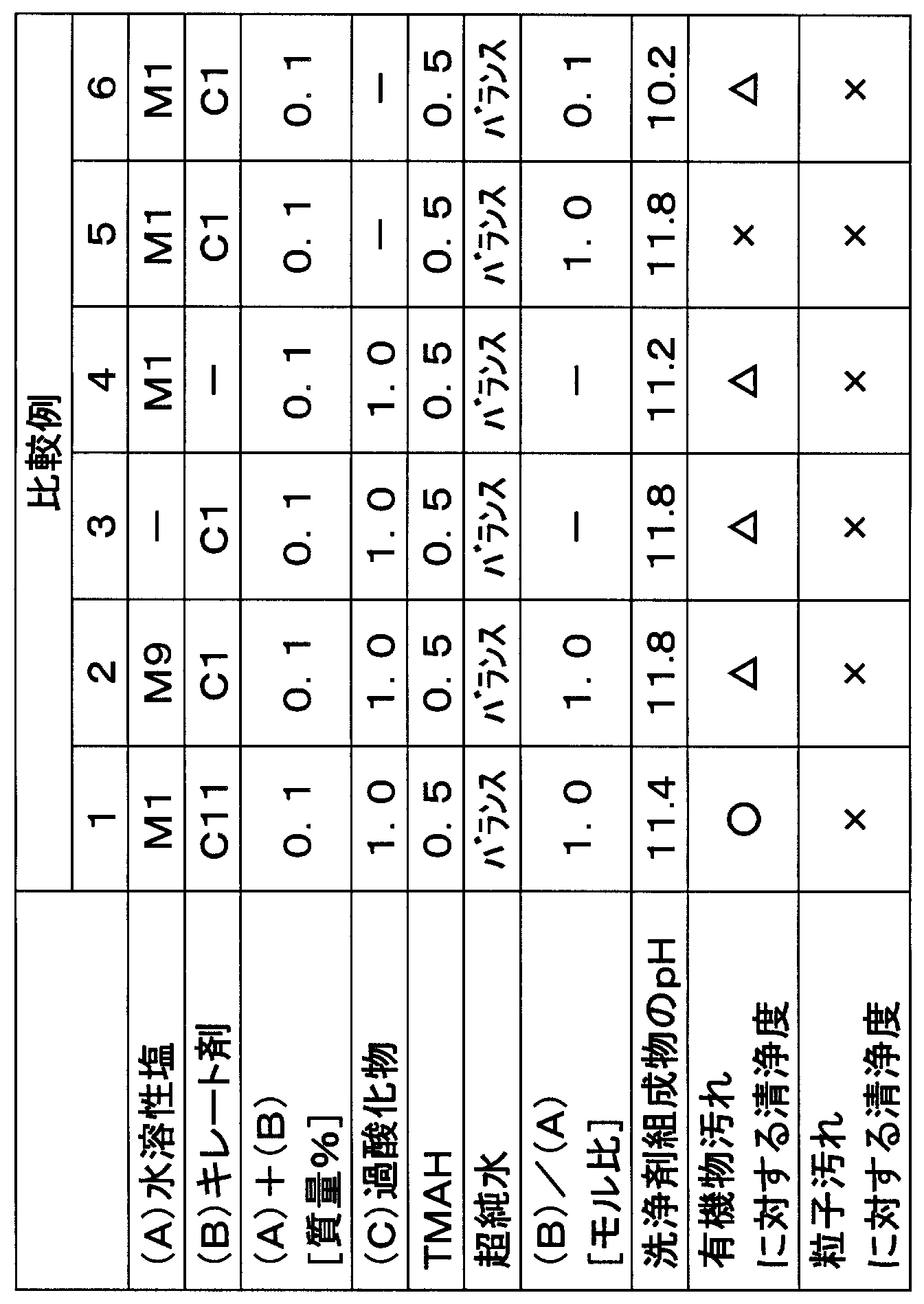
- M9 Calcium chloride dihydrate (Kanto Chemical Co., Ltd.), comparative component of component (A).
- C1 Iminodisuccinic acid tetrasodium salt (IDS-4Na, manufactured by LANXESS).
- C2 Hydroxyiminodisuccinic acid tetrasodium salt (HIDS-4Na, manufactured by Nippon Shokubai).
- C3 Methyl glycine diacetic acid trisodium salt (MGDA-3Na, trade name: Trilon M, manufactured by BASF).
- C4 L-glutamic acid diacetate tetrasodium salt (GLDA-4Na, manufactured by Cylest).
- C5 L-aspartic acid-N, N-diacetic acid tetrasodium salt (ASDA-4Na, manufactured by Mitsubishi Rayon).
- C6 Trisodium citrate dihydrate (Kanto Chemical, grade 1).
- C7 sodium tripolyphosphate (Kanto Chemical, grade 1).
- C8 Hydroxyethane diphosphonate sodium (trade name: BRIQUEST ADPA-60SH, manufactured by Rhodia).
- C9 Maleic acid acrylic acid copolymer (trade name: Socaran CP7, manufactured by BASF).
- C10 Carboxymethylated polyethyleneimine sodium salt (trade name: Trilon P, manufactured by BASF).
- C11 Sodium acetate (Wako Pure Chemicals, special grade), (B) component comparison component.
- TMAH tetramethylammonium hydroxide (trade name: TMAH-20H, manufactured by Toyo Gosei Co., Ltd.)
- Ultrapure water manufactured using GSR-200 (product name) manufactured by Advantech Toyo Co., Ltd. The specific resistance value of this ultrapure water at 25 ° C. was 18 M ⁇ ⁇ cm.
- the contact angle in the unwashed Si substrate after the mirror polishing treatment before the cleaning with the cleaning composition of each example was 42 degrees.
- FIG. 1A and 1B show AFM observation images of an uncleaned Si substrate after mirror polishing.
- 1A shows a shape image
- FIG. 1B shows a phase difference image.
- the hardness of the measurement surface can be determined based on the phase delay of cantilever vibration provided in the AFM.
- the organic substance is black because it is soft, and the inorganic substance is white because it is soft. Therefore, the presence of organic matter (organic matter stain) and inorganic matter (particle stain) can be confirmed on the Si substrate by such AFM observation.
- Example 27 to 33 Evaluation of cleanliness against metal stains was made by adding the component (A) at the end and mixing for 10 seconds in the above ⁇ Preparation of cleaning composition (1)>, and then immediately cleaning the cleaning composition of Example 1 obtained. This was used for the cleaning test shown below.
- Si substrate As the semiconductor substrate, an uncleaned Si substrate (manufactured by KN Platz) after mirror polishing was cut into 5 cm ⁇ 5 cm. (Cleaning method) The Si substrate cut into 5 cm ⁇ 5 cm was placed on a fluororesin dipper in a fluororesin beaker having a capacity of 1000 ml, and 700 ml of the cleaning composition of Example 1 was added. Subsequently, it adjusted to 50 degreeC and wash
- the Si substrate was put in another fluoropolymer beaker having a capacity of 1000 ml, and 700 ml of the acid cleaning agent of each example shown in Table 5 was added. Added each. Subsequently, it adjusted to 50 degreeC and wash
- isopropyl alcohol Kellocate, EL
- Evaluation criteria A 1 ⁇ 10 12 copper atoms / cm 2 or less (lower than the lower limit of quantification).
- ⁇ More than 1 ⁇ 10 15 copper atoms / cm 2 .
- the cleaning composition of Example 54 was prepared as follows according to a conventional method.
- a quartz beaker (diameter 60 mm, height 70 mm) containing a magnetic stirrer is charged with a predetermined amount of ultrapure water, adjusted to a temperature of 25 ° C., and a predetermined amount of chelating agent (B) while rotating the magnetic stirrer.
- C1 and M1 of a water-soluble salt (A) containing a transition metal were mixed to obtain a metal complex aqueous solution.
- NaOH and peroxide (C) were sequentially added to this aqueous metal complex solution to obtain a cleaning composition.
- the unit of the blending amount is mass%, and the blending amount of each component indicates the amount equivalent to the pure component.
- “Balance”, “(A) + (B) [mass%]”, and “(B) / (A) [molar ratio]” in the table are the same as above. Below, the component shown in the table
- Chelating agent (B) C12 nitrilotriacetic acid trisodium salt (Trilon A, manufactured by BASF).
- NaOH sodium hydroxide
- KOH Potassium hydroxide
- the silicon carbide substrate was removed from the polishing machine, washed with 100 ml of ultrapure water and then dried to prepare a contaminated silicon carbide substrate. And what used the said contaminated silicon carbide board
- the cut contaminated silicon carbide substrate was put into a quartz cell having a capacity of 7 ml obliquely so as not to contact the bottom surface and wall surface of the quartz cell, and 5 mL of the cleaning composition of each example was added thereto. Subsequently, it adjusted to 80 degreeC and wash
- the uncleaned contaminated silicon carbide substrate As the semiconductor substrate, the uncleaned contaminated silicon carbide substrate (size 2 inches) was used. (Cleaning method) The contaminated silicon carbide substrate was placed in a fluororesin dipper in a fluororesin beaker having a capacity of 1000 ml, and 700 ml of the cleaning composition of Example 34 was added. Subsequently, it adjusted to 80 degreeC and wash
- the contaminated silicon carbide substrate was taken out and rinsed for 1 minute in another 1000 ml fluororesin beaker while overflowing the running water of the ultrapure water. Thereafter, the contaminated silicon carbide substrate is taken out, and the contaminated silicon carbide substrate is immersed in isopropyl alcohol (Kanto Chemical, EL) heated to 50 ° C. in another fluoropolymer beaker having a capacity of 1000 ml. The contaminated silicon carbide substrate was taken out while being slowly pulled up at a rate of minutes and dried to obtain a silicon carbide substrate for evaluation.
- isopropyl alcohol Kellocate, EL
- the amount of copper atoms remaining on the surface of the silicon carbide substrate for evaluation was quantified in the same manner as described above, and the measurement was performed based on the following evaluation criteria. The results are shown in the table.
- the quantitative value of the copper atom in the silicon carbide substrate for evaluation before washing with the acid detergent of each example (unwashed) is about 9 ⁇ 10 15 copper atoms / cm 2 (1 ⁇ 10 15 copper atoms / cm 2).
- Copper atoms were quantified by creating a calibration curve using a Si standard sample.
- Evaluation criteria A 1 ⁇ 10 12 copper atoms / cm 2 or less (lower than the lower limit of quantification).
- ⁇ More than 1 ⁇ 10 15 copper atoms / cm 2 .
- both organic contaminants and particle contaminants attached to the electronic device substrate can be removed with high cleanliness, and the load on the environment Can be reduced.
Landscapes
- Chemical & Material Sciences (AREA)
- Engineering & Computer Science (AREA)
- Organic Chemistry (AREA)
- Wood Science & Technology (AREA)
- Oil, Petroleum & Natural Gas (AREA)
- Chemical Kinetics & Catalysis (AREA)
- Life Sciences & Earth Sciences (AREA)
- Inorganic Chemistry (AREA)
- Computer Hardware Design (AREA)
- Power Engineering (AREA)
- Microelectronics & Electronic Packaging (AREA)
- Physics & Mathematics (AREA)
- Manufacturing & Machinery (AREA)
- General Physics & Mathematics (AREA)
- Condensed Matter Physics & Semiconductors (AREA)
- Health & Medical Sciences (AREA)
- Emergency Medicine (AREA)
- Detergent Compositions (AREA)
- Cleaning Or Drying Semiconductors (AREA)
- Cleaning By Liquid Or Steam (AREA)
Abstract
Description
本願は、2008年2月15日に、日本に出願された特願2008-035165号に基づき優先権を主張し、その内容をここに援用する。
当該汚れとしては、ワックス等の基板固定剤などに由来する有機物汚れ、コロイダルシリカ等の研磨剤などに由来する粒子汚れ、Fe、Na、Cu等の金属もしくは金属イオンに由来する金属汚れ又はこれらの混合物等が挙げられる。
たとえば、半導体基板を洗浄対象とする精密洗浄では、過酸化水素および強酸(硫酸、塩酸など)と、過酸化水素およびアルカリ(アンモニアなど)と、フッ化水素酸とにより洗浄処理を行う方法、いわゆる「RCA洗浄」と呼ばれる洗浄方法が広く用いられている(たとえば、非特許文献1参照)。
また、RCA洗浄以外の洗浄方法として、オゾンの酸化力を用いて有機物汚れを除去する洗浄方法が提案されている(たとえば、特許文献1参照)。
RCA Review,p.187,June 1970
また、「RCA洗浄」は、一般的に、過酸化水素および強酸、過酸化水素およびアルカリ、並びにフッ化水素酸による洗浄処理(複数の洗浄ステップ)をそれぞれ行った後、多量の超純水を使用して複数回のすすぎ処理を行うプロセス(多槽浸漬式プロセス)が採用されているため、環境への負荷が大きい洗浄方法である。
一方、オゾンの酸化力を用いた洗浄方法においては、粒子汚れに対する清浄度が不充分である。
したがって、工業用分野の精密洗浄において、従来の洗浄方法に代わる新規な精密洗浄の方法が求められる。
すなわち、本発明は、電子デバイス用基板の洗浄に用いる洗浄剤組成物において、遷移金属を含む水溶性塩(A)と、キレート剤(B)と、過酸化物(C)とを含有し、かつ、前記キレート剤(B)の割合は、前記遷移金属を含む水溶性塩(A)に対して0.5モル当量以上であることを特徴とする洗浄剤組成物である。
また、本発明の洗浄剤組成物においては、pHが8以上であることが好ましい。
また、本発明の洗浄剤組成物においては、前記遷移金属を含む水溶性塩(A)と前記キレート剤(B)との全体の割合が0.01質量%以上であることが好ましい。
また、本発明の洗浄剤組成物においては、前記電子デバイス用基板が、半導体基板、ハードディスク基板、又はディスプレイ基板であることが好ましい。
前記半導体基板の材料は、ケイ素、炭化ケイ素、酸化亜鉛、又はサファイアであることが好ましい。
前記ハードディスク基板の材料は、ガラス、ニッケルとリンとの混合物、ニッケルと鉄との混合物、又はアルミニウムであることが好ましい。
前記ディスプレイ基板の材料はガラスであることが好ましい。
本発明の電子デバイス用基板の洗浄方法においては、洗浄時に超音波処理を行うことが好ましい。
また、本発明の電子デバイス用基板の洗浄方法においては、上記本発明の洗浄剤組成物を用いて洗浄した後、酸を用いて洗浄する工程を含むことが好ましい。
本発明の洗浄剤組成物は、電子デバイス用基板の洗浄に用いるものであり、遷移金属を含む水溶性塩(A)と、キレート剤(B)と、過酸化物(C)とを含有する。
遷移金属を含む水溶性塩(A)(以下「(A)成分」という。)において、遷移金属としては、長周期型周期表における3~11族の金属元素がつくる単体が挙げられる。なかでも、電子デバイス用基板に付着した有機物汚れおよび粒子汚れの両方に対してより高い清浄度が得られやすいことから、銅、鉄、マンガン、コバルト、ニッケル、銀が好ましく、銅、鉄、マンガン、コバルトがより好ましく、銅が特に好ましい。
水溶性塩としては、硫酸塩、塩化物、硝酸塩、臭素酸塩などが挙げられ、水等の溶媒への溶解性が特に良好であることから、硫酸塩、塩化物、硝酸塩が好ましく、硫酸塩がより好ましい。
(A)成分として具体的には、硫酸銅、硫酸鉄、硫酸マンガン、硫酸コバルト、硫酸ニッケル、硫酸銀等の硫酸塩;塩化銅、塩化鉄、塩化マンガン、塩化コバルト、塩化ニッケル等の塩化物;硝酸銅、硝酸鉄、硝酸マンガン、硝酸コバルト、硝酸ニッケル、硝酸銀等の硝酸塩;臭化銅、臭化鉄、臭化マンガン、臭化コバルト、臭化ニッケル等の臭素酸塩が挙げられる。
また、(A)成分としては、上記化合物に加えて、上記化合物の水和物も用いることができる。
(A)成分は、1種単独で、又は2種以上を適宜組み合わせて用いることができる。
キレート剤(B)(以下「(B)成分」という。)としては、たとえば、ニトリロトリ酢酸塩、エチレンジアミンテトラ酢酸塩、β-アラニンジ酢酸塩、グルタミン酸ジ酢酸塩、アスパラギン酸ジ酢酸塩、メチルグリシンジ酢酸塩、イミノジコハク酸塩、ジエチレントリアミンペンタ酢酸塩等のアミノカルボン酸塩;セリンジ酢酸塩、ヒドロキシイミノジコハク酸塩、ヒドロキシエチルエチレンジアミン三酢酸塩、ジヒドロキシエチルグリシン塩等のヒドロキシアミノカルボン酸塩;ヒドロキシ酢酸塩、クエン酸塩、グルコン酸塩等のヒドロキシカルボン酸塩;ピロメリット酸塩、ベンゾポリカルボン酸塩、シクロペンタンテトラカルボン酸塩等のシクロカルボン酸塩;カルボキシメチルタルトロン酸塩、カルボキシメチルオキシコハク酸塩、オキシジコハク酸塩、酒石酸モノコハク酸塩、酒石酸ジコハク酸塩等のエーテルカルボン酸塩;マレイン酸アクリル酸共重合体、カルボキシメチル化ポリエチレンイミン等の高分子キレート剤;トリポリリン酸ナトリウム、ヒドロキシエタンジホスホン酸、ピロリン酸等のリン系キレート剤などが挙げられる。
なかでも、(B)成分としては、電子デバイス用基板に付着した有機物汚れおよび粒子汚れの両方に対してより高い清浄度が得られやすいことから、ポリカルボン酸系化合物が好ましい。
ポリカルボン酸系化合物の中でより好適なものとしては、ニトリロトリ酢酸塩、エチレンジアミンテトラ酢酸塩、β-アラニンジ酢酸塩、グルタミン酸ジ酢酸塩、アスパラギン酸ジ酢酸塩、メチルグリシンジ酢酸塩、イミノジコハク酸塩、ジエチレントリアミンペンタ酢酸塩等のアミノポリカルボン酸塩;セリンジ酢酸塩、ヒドロキシイミノジコハク酸塩、ヒドロキシエチルエチレンジアミン三酢酸塩等のヒドロキシアミノポリカルボン酸塩;クエン酸塩等のヒドロキシポリカルボン酸塩;ピロメリット酸塩、ベンゾポリカルボン酸塩、シクロペンタンテトラカルボン酸塩等のシクロポリカルボン酸塩;カルボキシメチルタルトロン酸塩、カルボキシメチルオキシコハク酸塩、オキシジコハク酸塩、酒石酸モノコハク酸塩、酒石酸ジコハク酸塩等のエーテルポリカルボン酸塩;マレイン酸アクリル酸共重合体、カルボキシメチル化ポリエチレンイミン等の高分子キレート剤などが挙げられる。
(B)成分の割合の上限値は高いほど、(A)成分から放出される遷移金属の電子デバイス用基板への残留が抑制されるため好ましく、上限値としては、実質的に100モル当量以下であることが好ましく、10モル当量以下であることがより好ましい。(B)成分の割合が上限値以下であると、(B)成分の電子デバイス用基板への残留による有機物汚染も抑制しやすくなる。
なお、(B)成分の(A)成分に対する割合は、モル比[(B)/(A)]で表すことができる。
(A)成分と(B)成分との全体の割合が0.01質量%以上であると、電子デバイス用基板に付着した有機物汚れおよび粒子汚れの両方に対してより高い清浄度が得られやすくなる。当該全体の割合が5質量%以下であると、水溶液中で後述する(C)成分から発生する過酸化水素の分解による発泡を適度に制御でき、過酸化水素の失活が早まることを抑制できる。
本明細書および本特許請求の範囲において、「過酸化物」には、過酸化水素を包含するものとする。
過酸化物(C)(以下「(C)成分」という。)としては、過酸化水素、又は水溶液中で過酸化水素を発生するものであればよく、たとえば、過酸化水素、過炭酸、過ホウ酸、又はこれらのアルカリ金属塩(ナトリウム塩、カリウム塩など)もしくはアンモニウム塩などが挙げられる。なかでも、電子デバイス用基板に付着した有機物汚れおよび粒子汚れの両方に対してより高い清浄度が得られやすいことから、過酸化水素、過炭酸ナトリウム、過ホウ酸ナトリウムであることが好ましく、過酸化水素であることがより好ましい。
(C)成分は、1種単独で、又は2種以上を適宜組み合わせて用いることができる。
本発明の洗浄剤組成物における(C)成分の割合は、洗浄対象とする電子デバイス用基板の種類若しくは電子デバイス用基板の汚れ度合に応じて適宜調整すればよく、0.05~30質量%であることが好ましく、0.05~15質量%であることがより好ましく、0.1~10質量%であることがさらに好ましい。(C)成分の割合が0.05質量%以上であると、電子デバイス用基板に付着した有機物汚れおよび粒子汚れの両方に対してより高い清浄度が得られやすくなる。(C)成分の割合が30質量%以下、好ましくは15質量%以下であると、水溶液中で発生する過酸化水素量が抑制され、過酸化水素の分解による発泡を適度に制御できる。
たとえば、半導体基板である炭化ケイ素基板を洗浄する場合、本発明の洗浄剤組成物における(C)成分の割合は0.05~30質量%であることが好ましく、0.1~30質量%であることがより好ましい。(C)成分の割合が0.05質量%以上であると、炭化ケイ素基板に付着した有機物汚れおよび粒子汚れの両方に対してより高い清浄度が得られやすくなる。(C)成分の割合が30質量%以下であると、前記発泡を適度に制御できる。
なお、(C)成分の割合は高いほど、難分解性の汚れに対する洗浄性が向上する。
本発明の洗浄剤組成物においては、必要に応じて、上記の(A)成分、(B)成分および(C)成分以外のその他の成分を併用してもよい。
その他の成分としては、アルカリ剤、溶媒、界面活性剤等が挙げられる。
アルカリ剤としては、アンモニア、水酸化カリウム、水酸化ナトリウム等の無機アルカリ剤;テトラメチルアンモニウムヒドロキシド、テトラエチルアンモニウムヒドロキシド等の有機アルカリ剤が挙げられる。
溶媒としては、超純水、純水、エタノール、イソプロピルアルコール等が挙げられる。
界面活性剤としては、特に限定されず、直鎖アルキルベンゼンスルホン酸塩、アルキル硫酸塩、アルキルエーテル硫酸塩などのアニオン界面活性剤;高級アルコールのアルキレンオキシド付加物、プルロニック型界面活性剤などのノニオン界面活性剤等が挙げられる。
その際、(A)成分と(B)成分は、両方の成分同士を予め混合して乾燥させた混合物として用いてもよく、それぞれ別個に配合してもよい。又は、(A)成分と(B)成分とを混合して形成される金属錯体(錯化合物、錯塩)を配合してもよい。
また、(A)成分と(C)成分は、配合順序が離れていることが好ましい。これにより、(C)成分から発生する過酸化水素の分解を抑制でき、より安定に洗浄剤組成物を調製できる。
また、(C)成分と(A)成分とを、洗浄を行う直前に混合することも好ましい。
また、アルカリ剤を用いる場合、(C)成分とアルカリ剤とを、洗浄を行う直前に混合することが好ましい。これにより、(C)成分から発生する過酸化水素の分解を抑制でき、より安定に洗浄剤組成物を調製できる。
さらに、上記調製方法以外に、(C)成分を含む調製物と(A)成分を含む調製物とを予め準備し、洗浄を行う際に両方の調製物同士を混合してもよい。かかる場合、(B)成分は、いずれの調製物に含まれていてもよい。
さらに、上記調製方法以外に、(C)成分を含む調製物と(B)成分を含む調製物と(A)成分を含む調製物とを予め準備し、洗浄を行う際に前記の調製物同士を混合してもよい。また、(A)成分を含む調製物と(C)成分を含む調製物は、混合順序が離れていることが好ましい。これにより、(C)成分から発生する過酸化水素の分解を抑制でき、より安定に洗浄剤組成物を調製できる。
上記洗浄剤組成物(原液)のpHは、洗浄剤組成物を調製した直後から25℃で10分間放置した後の洗浄剤組成物(原液)のpHを示す。
pHの測定は、pHメータ(製品名:HM-20S、東亜ディーケーケー株式会社製)とpH電極(製品名:GST-5211C、東亜ディーケーケー株式会社製)を用いて、約25℃の洗浄剤組成物に対してpH電極を浸漬し15秒経過後の指示値を読み取ることにより行う。
なお、本発明の洗浄剤組成物は、(A)~(C)成分の相互作用により、調製直後のpHの値が一定しない。そのため、本発明においては、洗浄剤組成物のpHがほぼ一定値を示す、調製後から10分後の洗浄剤組成物(原液)のpHを測定するものとする。
本発明の洗浄剤組成物は、電子デバイス用基板の洗浄に用いるものである。
電子デバイス用基板としては、半導体基板、ハードディスク基板、又はディスプレイ基板であることが好ましい。本発明の洗浄剤組成物は、特に、これら基板を損傷させることなく、当該基板に付着した汚れを非常に高い清浄度で除去することができる。
前記ハードディスク基板の材料としては、ガラス、ニッケルとリンとの混合物(Ni-P)、ニッケルと鉄との混合物(Ni-Fe)、アルミニウム、炭化ホウ素、炭素等が挙げられ、なかでもガラス、ニッケルとリンとの混合物(Ni-P)、ニッケルと鉄との混合物(Ni-Fe)、又はアルミニウムであることが好ましい。
前記ディスプレイ基板の材料としては、ガラス、プラスチック等が挙げられ、なかでもガラスであることが好ましい。
本発明の洗浄剤組成物は、上記の材料を用いた各種の電子デバイス用基板に付着した汚れを非常に高い清浄度で除去することができ、当該基板の精密洗浄に用いる洗浄剤組成物として特に好適である。
かかる効果が得られる理由としては、定かではないが以下のように推測される。
本発明の洗浄剤組成物は、遷移金属を含む水溶性塩(A)と、キレート剤(B)と、過酸化物(C)とを含有し、かつ、(A)成分に対して0.5モル当量以上の(B)成分を含有する。
洗浄剤組成物中又は洗浄時、(A)成分と(B)成分は、金属錯体(錯化合物、錯塩)を形成する。特に、(B)成分の割合を、(A)成分に対して0.5モル当量以上とすることで、金属錯体を良好に形成できる。そして、当該金属錯体は、(C)成分から発生する過酸化水素をより活性化する。これによって、本発明の洗浄剤組成物は、電子デバイス用基板に付着した有機物汚れおよび粒子汚れをいずれも高い清浄度で除去することができると考えられる。
本発明の洗浄剤組成物は、本来汚れとして除去すべき金属を、意図的に、さらに用いたものであり、これによって、特に有機物汚れおよび粒子汚れに対する洗浄効果が従来よりも格段に高まったものである。なお、電子デバイス用基板上の汚れとして存在する金属汚れに含まれる金属の量では、当該洗浄効果は得られない。
本発明の洗浄剤組成物は、電子デバイス用基板の洗浄に特に好適なものである。
本発明の電子デバイス用基板の洗浄方法は、上記本発明の洗浄剤組成物を用いる方法である。
当該洗浄方法としては、特に限定されるものではなく、洗浄対象とする電子デバイス用基板に、洗浄剤組成物をノズル等から直接吹き付けて塗布して拭き取る方法;電子デバイス用基板を洗浄剤組成物に浸漬する方法;洗浄時に超音波処理を行う方法などが挙げられる。
本発明の電子デバイス用基板の洗浄方法においては、洗浄時に超音波処理を行う方法が好ましい。洗浄時に超音波処理を行うと、電子デバイス用基板に付着した有機物汚れおよび粒子汚れの両方に対してより高い清浄度が得られる。特に、粒子汚れに対する清浄度が高まるため、好ましい。
以下、本発明の電子デバイス用基板の洗浄方法の一例について説明する。
次いで、上記本発明の洗浄剤組成物を入れて、電子デバイス用基板を洗浄剤組成物中に浸漬し、超音波振動子から超音波を発振する。
一定時間、超音波照射をした後、洗浄剤組成物から電子デバイス用基板を取り出す(以上「超音波洗浄工程」という)。
その後、取り出した電子デバイス用基板を、純水(好ましくは超純水)の流水ですすぎ、電子デバイス用基板に残存している洗浄剤組成物や汚れを除去する。この電子デバイス用基板に残存している洗浄剤組成物や汚れの除去は、底面に超音波振動子を備えたリンス槽に純水(好ましくは超純水)を入れ、この純水中に、超音波洗浄工程後の電子デバイス用基板を浸漬し、超音波振動子から超音波を発振させて行ってもよい(以上「リンス工程」という)。
リンス工程を終えた電子デバイス用基板は、乾燥機によって、電子デバイス用基板に残存した純水が除去される(以上「乾燥工程」という)。
また、電子デバイス用基板上の汚れとしては、ワックス等の基板固定剤、人体などに由来する有機物汚れ;コロイダルシリカ等の研磨剤、空気中の浮遊粒子などに由来する粒子汚れ;Fe、Na、Cu等の金属もしくは金属イオンに由来する金属汚れ、又はこれらの混合物等が挙げられる。このうち、本発明の電子デバイス用基板の洗浄方法は、特に、有機物汚れおよび粒子汚れの両方を除去するのに好適である。
洗浄剤組成物を希釈して用いる場合、その希釈倍率としては、2~1000倍とすることが好ましく、2~100倍とすることがより好ましい。当該希釈倍率の上限値以下であれば、有機物汚れおよび粒子汚れの両方を充分に除去できる。
例えば、超音波振動子における発振周波数は、200kHz以上2MHz以下が好ましく、500kHz以上1MHz以下がより好ましい。当該発振周波数が200kHz以上であると、超音波由来の機械力が強くなりすぎず、電子デバイス用基板をより傷めることなく、洗浄できる。当該発振周波数が2MHz以下であると、特に粒子汚れの除去効果が向上する。
超音波洗浄の時間は、特に限定されず、1~30分間が好ましく、5~15分間がより好ましい。
また、超音波洗浄中、洗浄槽内の温度は、特に限定されず、5~95℃が好ましく、15~80℃がより好ましい。当該温度が前記範囲であると、洗浄剤組成物が良好に溶存され、有機物汚れおよび粒子汚れに対する洗浄効果が安定に得られる。
また、リンス工程中の純水(好ましくは超純水)の温度は、特に限定されない。
本発明の電子デバイス用基板の洗浄方法によれば、上述した「RCA洗浄」のように、複数の洗浄ステップ間で、多量の超純水を使用して複数回のすすぎ処理を行う必要がなく、たとえば1バッチの浸漬洗浄が可能であるため、すすぎ処理回数を少なくでき、環境への負荷が小さい。また、簡便な方法でもある。
さらに、本発明の電子デバイス用基板の洗浄方法によれば、高濃度の強酸やアルカリ、又は毒性の強い水溶液であるフッ化水素酸を用いることなく、電子デバイス用基板に付着した有機物汚れおよび粒子汚れを、非常に高い清浄度で除去することができる。また、高濃度の強酸、高濃度のアルカリ、および毒性を有するフッ化水素酸等の薬剤を用いる必要がないため、洗浄における作業性が向上し、耐腐食もしくは排気等の設備が不要である。
また、本発明の電子デバイス用基板の洗浄方法によれば、有機物汚れおよび粒子汚れを同時に除去することができ、電子デバイス用基板を損傷することなく、精密洗浄を行うことが可能である。
この酸の種類は、有機酸であってもよく、無機酸であってもよく、金属汚れの除去能力が高く、酸自体の電子デバイス用基板への残留性が低い等の点から、無機酸であることが好ましい。この無機酸としては、たとえば硫酸、塩酸、硝酸、フッ化水素酸又はこれらの混合物を用いることができる。
使用する酸の濃度は、金属汚れの除去が可能であれば特に制限されるものではない。
また、金属汚れの除去効率が向上することから、酸を用いて洗浄する際にキレート剤を併用することが好ましい。このキレート剤の種類は、特に制限されるものではなく、たとえば上記(B)成分についての説明において例示したものを用いることができる。
本発明の電子デバイス用基板の洗浄方法においては、酸を用いて洗浄する工程を含む場合であっても、有機物汚れおよび粒子汚れを除去する際、高濃度の強酸、フッ化水素酸を用いる必要がないため、従来の「RCA洗浄」等に比べて酸の使用量を全体的に少なくでき、環境への負荷が低減されている。
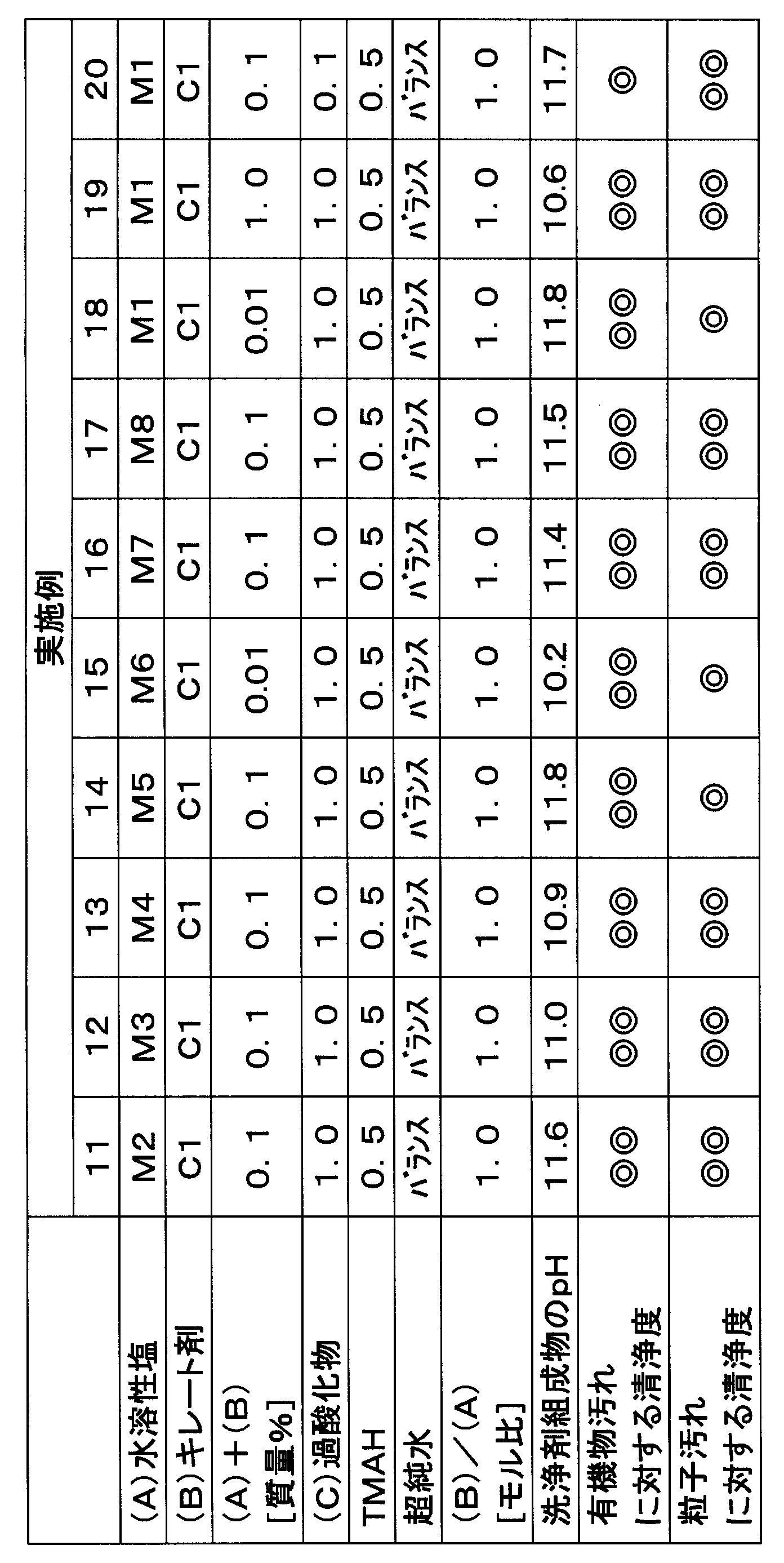
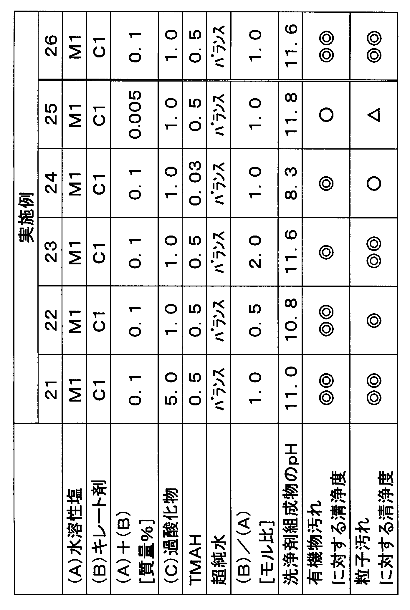
<洗浄剤組成物の調製(1)>
表1~4に示す組成の洗浄剤組成物(ただし、実施例26を除く。)を、常法に準じて、以下のようにして調製した。
マグネチックスターラーの入った石英ビーカー(直径60mm、高さ70mm)に、所定量の超純水を入れ、25℃に調温し、マグネチックスターラーを回転させながら、それぞれ所定量のキレート剤(B)、過酸化物(C)、TMAH、遷移金属を含む水溶性塩(A)を順次、配合して洗浄剤組成物を得た。
マグネチックスターラーの入った石英ビーカー(直径60mm、高さ70mm)に、所定量の超純水を入れ、25℃に調温し、マグネチックスターラーを回転させながら、所定量のキレート剤(B)のC1と、遷移金属を含む水溶性塩(A)のM1とを混合して水溶液(後述の金属錯体水溶液)を得た。
この水溶液の吸光度を、分光光度計(製品名:MultiSpec-1500、株式会社島津製作所製)により測定したところ、C1、M1それぞれ単独の水溶液には見られない新たなピークが波長310nm付近に現れたことから、C1とM1との間で錯体を形成していることを確認した。
この金属錯体水溶液に、TMAH、過酸化物(C)を順次、配合して洗浄剤組成物を得た。
表における「バランス」とは、洗浄剤組成物に含まれる各成分の総量が100質量%になるように配合した、洗浄剤組成物中の超純水の配合量を意味する。
表における「(A)+(B)[質量%]」は、洗浄剤組成物中の(A)成分と(B)成分との全体の割合[質量%]を示す。
また、表における「(B)/(A)[モル比]」は、(B)成分の(A)成分に対する割合(モル当量)を示す。
以下に、表中に示した成分について説明する。
・遷移金属を含む水溶性塩(A)
M1:硫酸銅5水和物(関東化学、1級)。
M2:硫酸鉄7水和物(関東化学、特級)。
M3:硫酸マンガン5水和物(関東化学、特級)。
M4:硫酸コバルト7水和物(和光純薬)。
M5:硫酸ニッケル6水和物(純正化学、特級)。
M6:硫酸銀(関東化学、1級)。
M7:塩化銅(II)2水和物(関東化学、1級)。
M8:硝酸銅(II)3水和物(関東化学、1級)。
M9:塩化カルシウム2水和物(関東化学、特級)、(A)成分の比較成分。
C1:イミノジコハク酸4ナトリウム塩(IDS-4Na、ランクセス製)。
C2:ヒドロキシイミノジコハク酸4ナトリウム塩(HIDS-4Na、日本触媒製)。
C3:メチルグリシンジ酢酸3ナトリウム塩(MGDA-3Na、商品名:Trilon M、BASF製)。
C4:L-グルタミン酸ジ酢酸4ナトリウム塩(GLDA-4Na、キレスト製)。
C5:L-アスパラギン酸-N,N-二酢酸4ナトリウム塩(ASDA-4Na、三菱レイヨン製)。
C6:クエン酸三ナトリウム2水和物(関東化学、1級)。
C7:トリポリリン酸ナトリウム(関東化学、1級)。
C8:ヒドロキシエタンジホスホン酸ナトリウム(商品名:BRIQUEST ADPA-60SH、ローディア製)。
C9:マレイン酸アクリル酸共重合物(商品名:ソカランCP7、BASF製)。
C10:カルボキシメチル化ポリエチレンイミン ナトリウム塩(商品名:Trilon P、BASF製)。
C11:酢酸ナトリウム(和光純薬、特級)、(B)成分の比較成分。
過酸化水素:関東化学、特級。
TMAH:テトラメチルアンモニウムヒドロキシド(商品名:TMAH-20H、東洋合成工業製)。
超純水:アドバンテック東洋(株)製のGSR-200(製品名)を用いて製造したもの。この超純水の25℃における比抵抗値は18MΩ・cmであった。
上記<洗浄剤組成物の調製(1)>において、最後に(A)成分を加えて(実施例26については最後に(C)成分を加えて)10秒間混合した後、得られる洗浄剤組成物10mLを直ちにサンプル瓶に取り、蓋をせず25℃で10分間放置した後、当該洗浄剤組成物(原液)のpHを測定した。
pHの測定は、pHメータ(製品名:HM-20S、東亜ディーケーケー株式会社製)とpH電極(製品名:GST-5211C、東亜ディーケーケー株式会社製)を用いて、約25℃の洗浄剤組成物に対してpH電極を浸漬し15秒経過後の指示値を読み取ることにより行った。
有機物汚れおよび粒子汚れに対する清浄度の評価は、上記<洗浄剤組成物の調製(1)>において、最後に(A)成分を加えて(実施例26については最後に(C)成分を加えて)10秒間混合した後、得られる洗浄剤組成物を直ちに、以下に示す洗浄試験に用いてそれぞれ行った。
(電子デバイス用基板)
半導体基板として、鏡面研磨処理後の未洗浄のSi基板(KNプラッツ製)を5cm×2cmにカットしたものを用いた。
(洗浄方法)
上記のカットしたSi基板1枚を、100mLの石英ビーカーに、当該石英ビーカー底面に接しないように斜めに固定して入れ、各例の洗浄剤組成物50mLをそれぞれ加えた。
次いで、50℃に調整し、600kHzの超音波を印加する超音波処理を行いながら10分間洗浄した。
洗浄後、前記超純水の流水により30秒間すすいだ後、窒素ブローで乾燥し、評価用Si基板を得た。
上記で得た評価用Si基板の表面に、前記超純水2μLを滴下し、接触角計(製品名:接触角計CA-X型、協和界面科学株式会社製)を用いて、25℃における接触角の測定を行った。ただし、ここでいう「接触角」とは、静的接触角、すなわち、評価用Si基板表面と、水平に置いた評価用Si基板上の水滴表面とのなす角度を示す。
そして、測定した接触角を指標として、下記評価基準に基づいて、有機物汚れに対する清浄度を評価した。その結果を表に示す。
なお、各例の洗浄剤組成物による洗浄前の、鏡面研磨処理後の未洗浄のSi基板における接触角は42度であった。
評価基準
◎◎:7度以下。
◎:7度超15度以下。
○:15度超25度以下。
△:25度超35度以下。
×:35度超。
上記で得た評価用Si基板の表面を、走査型プローブ顕微鏡(AFM)(製品名:SPM-9500J3、株式会社島津製作所製)を用いて観察し、目視により、評価用Si基板の表面30μm×30μmの領域で検出される直径5nm以上の粒子の数を測定した。
そして、測定した粒子の数を指標として、下記評価基準に基づいて、粒子汚れに対する清浄度を評価した。その結果を表に示す。
なお、各例の洗浄剤組成物による洗浄前の、鏡面研磨処理後の未洗浄のSi基板における粒子の数は約500個であった。
評価基準
◎◎:0~10個。
◎:11~50個。
○:51~100個。
△:101~200個。
×:201個以上。
図1Aは形状像、図1Bは位相差像をそれぞれ示す。
AFM観察においては、AFMに備えられるカンチレバー振動の位相の遅れに基づいて測定面の硬軟を判断することができる。位相差像において、有機物は軟らかいため黒く見え、無機物は軟らかいため白く見える。
したがって、かかるAFM観察により、当該Si基板上に、有機物(有機物汚れ)および無機物(粒子汚れ)の存在を確認できる。

<金属汚れに対する清浄度の評価>
金属汚れに対する清浄度の評価は、上記<洗浄剤組成物の調製(1)>において、最後に(A)成分を加えて10秒間混合した後、得られる実施例1の洗浄剤組成物を直ちに、以下に示す洗浄試験に用いて行った。
(酸洗浄剤の調製)
酸洗浄剤として、表5に示す組成の酸水溶液をそれぞれ用いた。なお、表5中の配合量の単位は質量%であり、各成分の配合量はいずれも純分換算量を示す。
表における「バランス」とは、酸洗浄剤に含まれる各成分の総量が100質量%になるように配合した、酸洗浄剤中の超純水の配合量を意味する。
酸は、下記のものを使用し、前記超純水にそれぞれ溶解して調製した。
硫酸(関東化学、Ultrapur-100)。
硝酸(関東化学、Ultrapur-100)。
塩酸(関東化学、Ultrapur-100)。
フッ化水素酸(関東化学、Ultrapur-100)。
半導体基板として、鏡面研磨処理後の未洗浄のSi基板(KNプラッツ製)を5cm×5cmにカットしたものを用いた。
(洗浄方法)
容量1000mlのフッ素樹脂製ビーカーに、5cm×5cmにカットした前記Si基板をフッ素樹脂製ディッパーに乗せて入れ、実施例1の洗浄剤組成物700mlを加えた。次いで、50℃に調整し、浸漬による洗浄を10分間行った。洗浄後、当該Si基板を取り出して前記超純水の流水により30秒間すすいだ後、別の容量1000mlのフッ素樹脂製ビーカーに当該Si基板を入れ、表5に示す各例の酸洗浄剤700mlをそれぞれ加えた。次いで、50℃に調整し、浸漬による洗浄を10分間行った。洗浄後、当該Si基板を取り出して、別の容量1000mlのフッ素樹脂製ビーカーにて、前記超純水の流水をオーバーフローさせながら1分間すすいだ。その後、当該Si基板を取り出して、別の容量1000mlのフッ素樹脂製ビーカーにて、当該Si基板を、50℃に加温したイソプロピルアルコール(関東化学、EL)に浸漬し、1cm/分の速度で徐々に引き上げながら当該Si基板を取り出して乾燥させ、評価用Si基板を得た。
金属汚れに対する清浄度の評価は、株式会社リガク製の卓上型全反射蛍光X線分析装置NANOHUNTER(製品名)を用いて、評価用Si基板の表面に残存する銅原子の定量を行い、下記評価基準に基づいて実施した。その結果を表に示す。
なお、各例の酸洗浄剤による洗浄前(未洗浄)の、評価用Si基板における銅原子の定量値は、約9×10¹⁵銅原子/cm2(1×1015銅原子/cm2超)であった。銅原子の定量は、既知量の銅原子を付着させたSi標準試料を使用して検量線を作成することにより行った。
評価基準
◎◎:1×10¹²銅原子/cm2以下(定量下限以下)。
◎:1×10¹²銅原子/cm2超 1×10¹³銅原子/cm2以下。
○:1×10¹³銅原子/cm2超 1×10¹⁴銅原子/cm2以下。
△:1×10¹⁴銅原子/cm2超 1×10¹⁵銅原子/cm2以下。
×:1×10¹⁵銅原子/cm2超。
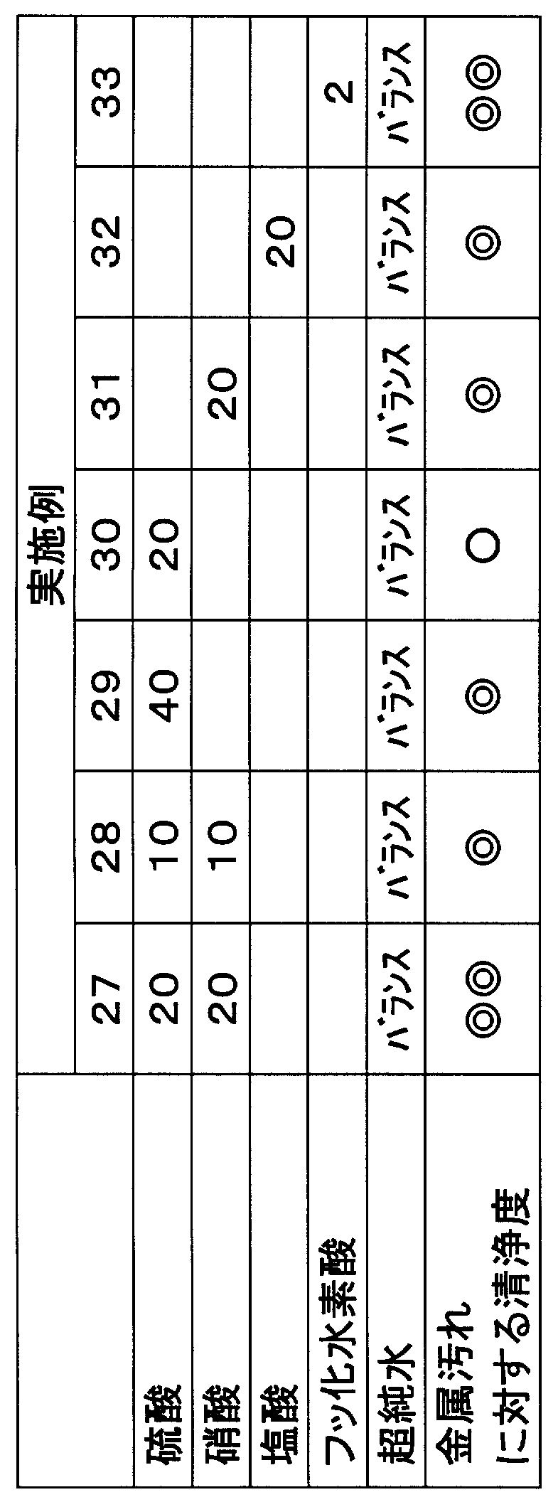
<洗浄剤組成物の調製(2)>
表6~9に示す組成の洗浄剤組成物(ただし、実施例54を除く。)を、常法に準じて、以下のようにして調製した。
マグネチックスターラーの入ったフッ素樹脂製ビーカー(直径60mm、高さ70mm)に、所定量の超純水を入れ、25℃に調温し、マグネチックスターラーを回転させながら、それぞれ所定量のキレート剤(B)、過酸化物(C)、アルカリ剤、遷移金属を含む水溶性塩(A)を順次、配合して洗浄剤組成物を得た。
マグネチックスターラーの入った石英ビーカー(直径60mm、高さ70mm)に、所定量の超純水を入れ、25℃に調温し、マグネチックスターラーを回転させながら、所定量のキレート剤(B)のC1と、遷移金属を含む水溶性塩(A)のM1とを混合して金属錯体水溶液を得た。
この金属錯体水溶液に、NaOH、過酸化物(C)を順次、配合して洗浄剤組成物を得た。
表における「バランス」、「(A)+(B)[質量%]」、「(B)/(A)[モル比]」は、上記と同じである。
以下に、表中に示した成分について説明する。
表6~9中に示した成分について、表1~4と共通の英数字、英字は、いずれも同じものを意味する。
C12:ニトリロトリ酢酸3ナトリウム塩(Trilon A、BASF製)。
NaOH:水酸化ナトリウム(関東化学、UGR)。
KOH:水酸化カリウム(関東化学、UGR)。
表6~9に示す各例の洗浄剤組成物のpHは、上記pHの測定と同様にして測定した。
有機物汚れおよび粒子汚れに対する清浄度の評価は、上記<洗浄剤組成物の調製(2)>において、最後に(A)成分を加えて(実施例54については最後に(C)成分を加えて)10秒間混合した後、得られる洗浄剤組成物を直ちに、以下に示す洗浄試験に用いてそれぞれ行った。
(電子デバイス用基板)
炭化ケイ素基板(新日本製鐵製;2インチ、商品名:ポリタイプ4H、Si面仕上げ研磨済み)を、ワックス(日化精工製、商品名:アルコワックス)で研磨盤に貼り付けて固定した。
研磨機(Buehler社製;製品名:AutoMet2000、EcoMet3000)を用い、研磨バフ(Buehler社製、商品名:MasterTex)にコロイダルシリカ研磨スラリー(Buehler社製、商品名:MasterMet)を滴下し、5ポンドの荷重を与えながら2分間研磨作業を行った。
当該炭化ケイ素基板を研磨盤から外し、超純水の流水100mlで洗浄後、乾燥させて汚染炭化ケイ素基板を作製した。
そして、半導体基板として、当該汚染炭化ケイ素基板を1cm×1cmにカットしたものを用いた。
カットした汚染炭化ケイ素基板を、容量7mlの石英セルに、当該石英セル底面と壁面に接しないように斜めに固定して入れ、各例の洗浄剤組成物5mLをそれぞれ加えた。次いで、80℃に調整し、浸漬による洗浄を30分間行った。
洗浄後、前記超純水の流水により30秒間すすいだ後、窒素ブローで乾燥し、評価用炭化ケイ素基板を得た。
評価用Si基板の代わりに評価用炭化ケイ素基板を用いた以外は、上記と同様にして、25℃における接触角の測定を行った。
そして、測定した接触角を指標として、下記評価基準に基づいて、有機物汚れに対する清浄度を評価した。その結果を表に示す。
なお、各例の洗浄剤組成物による洗浄前の、未洗浄の前記汚染炭化ケイ素基板における接触角は70度であった。
評価基準
◎◎:45度以下。
◎:45度超50度以下。
○:50度超55度以下。
△:55度超60度以下。
×:60度超。
評価用Si基板の代わりに評価用炭化ケイ素基板を用いた以外は、上記と同様にして、評価用炭化ケイ素基板の表面30μm×30μmの領域で検出される直径5nm以上の粒子の数を測定した。
そして、測定した粒子の数を指標として、下記評価基準に基づいて、粒子汚れに対する清浄度を評価した。その結果を表に示す。
なお、各例の洗浄剤組成物による洗浄前の、未洗浄の前記汚染炭化ケイ素基板における粒子の数は約500個であった。
評価基準
◎◎:0~10個。
◎:11~50個。
○:51~100個。
△:101~200個。
×:201個以上。
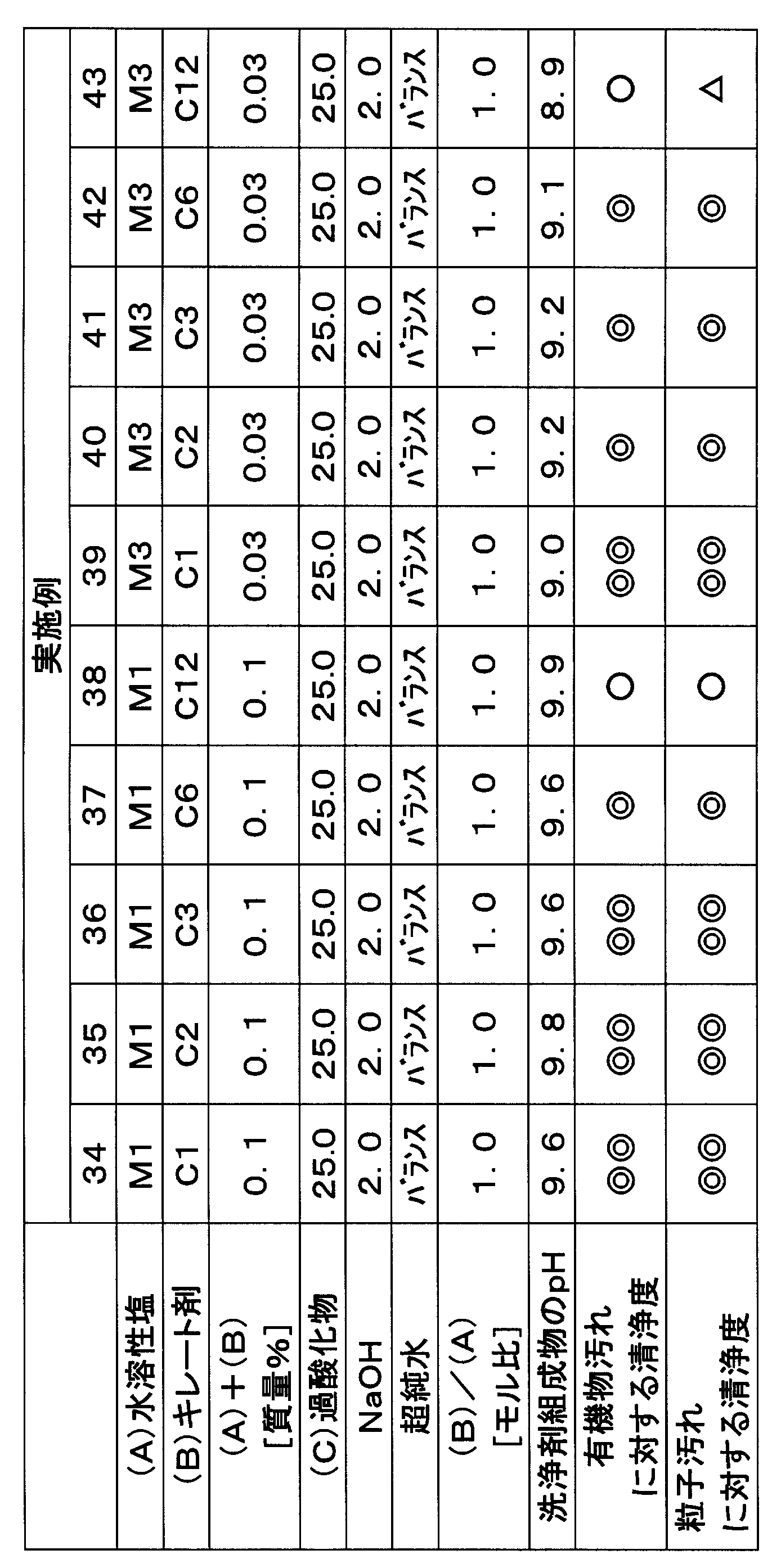

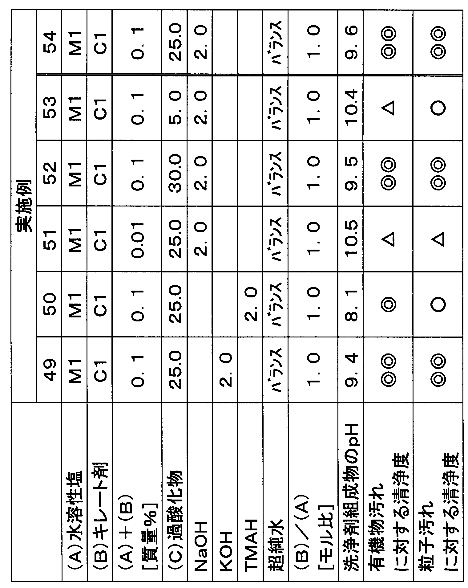
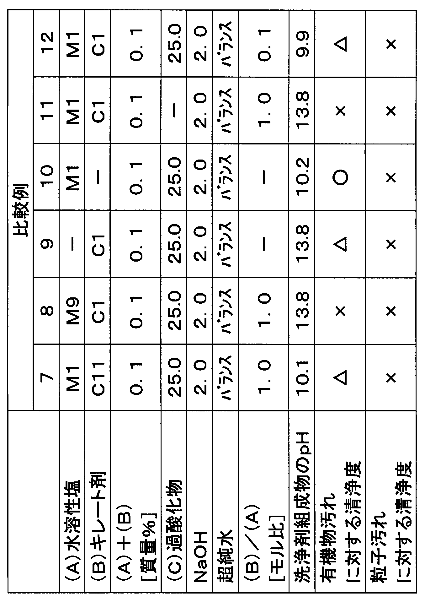
<金属汚れに対する清浄度の評価>
金属汚れに対する清浄度の評価は、上記<洗浄剤組成物の調製(2)>において、最後に(A)成分を加えて10秒間混合した後、得られる実施例34の洗浄剤組成物を直ちに、以下に示す洗浄試験に用いて行った。
(酸洗浄剤の調製)
酸洗浄剤として、表10に示す組成の酸水溶液をそれぞれ用いた。当該酸水溶液は、表5に示すものと同様にして調製した。
半導体基板として、未洗浄の前記汚染炭化ケイ素基板(大きさ2インチ)を用いた。
(洗浄方法)
容量1000mlのフッ素樹脂製ビーカーに、前記汚染炭化ケイ素基板をフッ素樹脂製ディッパーに乗せて入れ、実施例34の洗浄剤組成物700mlを加えた。次いで、80℃に調整し、浸漬による洗浄を30分間行った。洗浄後、当該汚染炭化ケイ素基板を取り出して前記超純水の流水により30秒間すすいだ後、別の容量1000mlのフッ素樹脂製ビーカーに当該汚染炭化ケイ素基板を入れ、表10に示す各例の酸洗浄剤700mlをそれぞれ加えた。次いで、80℃に調整し、浸漬による洗浄を10分間行った。洗浄後、当該汚染炭化ケイ素基板を取り出して、別の容量1000mlのフッ素樹脂製ビーカーにて、前記超純水の流水をオーバーフローさせながら1分間すすいだ。その後、当該汚染炭化ケイ素基板を取り出して、別の容量1000mlのフッ素樹脂製ビーカーにて、当該汚染炭化ケイ素基板を、50℃に加温したイソプロピルアルコール(関東化学、EL)に浸漬し、1cm/分の速度で徐々に引き上げながら当該汚染炭化ケイ素基板を取り出して乾燥させ、評価用炭化ケイ素基板を得た。
評価用Si基板の代わりに評価用炭化ケイ素基板を用いた以外は、上記と同様にして、評価用炭化ケイ素基板の表面に残存する銅原子の定量を行い、下記評価基準に基づいて実施した。その結果を表に示す。
なお、各例の酸洗浄剤による洗浄前(未洗浄)の、評価用炭化ケイ素基板における銅原子の定量値は、約9×10¹⁵銅原子/cm2(1×1015銅原子/cm2超)であった。銅原子の定量は、Si標準試料を使用して検量線を作成することにより行った。
評価基準
◎◎:1×10¹²銅原子/cm2以下(定量下限以下)。
◎:1×10¹²銅原子/cm2超 1×10¹³銅原子/cm2以下。
○:1×10¹³銅原子/cm2超 1×10¹⁴銅原子/cm2以下。
△:1×10¹⁴銅原子/cm2超 1×10¹⁵銅原子/cm2以下。
×:1×10¹⁵銅原子/cm2超。

Claims (12)
- 電子デバイス用基板の洗浄に用いる洗浄剤組成物において、
遷移金属を含む水溶性塩(A)と、キレート剤(B)と、過酸化物(C)とを含有し、かつ、前記キレート剤(B)の割合は、前記遷移金属を含む水溶性塩(A)に対して0.5モル当量以上であることを特徴とする洗浄剤組成物。 - 前記キレート剤(B)がポリカルボン酸系化合物である請求項1記載の洗浄剤組成物。
- pHが8以上である請求項1又は請求項2記載の洗浄剤組成物。
- 前記遷移金属を含む水溶性塩(A)と前記キレート剤(B)との全体の割合が0.01質量%以上である請求項1~3のいずれかに記載の洗浄剤組成物。
- 前記電子デバイス用基板が、半導体基板、ハードディスク基板、又はディスプレイ基板である請求項1~4のいずれかに記載の洗浄剤組成物。
- 前記半導体基板の材料は、ケイ素、炭化ケイ素、酸化亜鉛、又はサファイアである請求項5記載の洗浄剤組成物。
- 前記ハードディスク基板の材料は、ガラス、ニッケルとリンとの混合物、ニッケルと鉄との混合物、又はアルミニウムである請求項5記載の洗浄剤組成物。
- 前記ディスプレイ基板の材料はガラスである請求項5記載の洗浄剤組成物。
- 請求項1~8のいずれかに記載の洗浄剤組成物を用いることを特徴とする電子デバイス用基板の洗浄方法。
- 洗浄時に超音波処理を行う請求項9記載の電子デバイス用基板の洗浄方法。
- 前記洗浄剤組成物を用いて洗浄した後、酸を用いて洗浄する工程を含む請求項9又は請求項10記載の電子デバイス用基板の洗浄方法。
- 請求項9~11のいずれかに記載の洗浄方法を用いて製造された電子デバイス用基板。
Priority Applications (4)
| Application Number | Priority Date | Filing Date | Title |
|---|---|---|---|
| US12/867,468 US8809247B2 (en) | 2008-02-15 | 2009-02-13 | Cleaning composition and method for cleaning substrate for electronic device |
| JP2009553454A JP5286290B2 (ja) | 2008-02-15 | 2009-02-13 | 洗浄剤組成物および電子デバイス用基板の洗浄方法、並びに電子デバイス用基板 |
| EP09710545A EP2244283A4 (en) | 2008-02-15 | 2009-02-13 | CLEANING COMPOSITION AND METHOD FOR CLEANING SUBSTRATE FOR ELECTRONIC DEVICE |
| CN200980105412.9A CN101946310B (zh) | 2008-02-15 | 2009-02-13 | 清洗剂组合物及电子设备用基板的清洗方法 |
Applications Claiming Priority (2)
| Application Number | Priority Date | Filing Date | Title |
|---|---|---|---|
| JP2008035165 | 2008-02-15 | ||
| JP2008-035165 | 2008-02-15 |
Publications (1)
| Publication Number | Publication Date |
|---|---|
| WO2009102004A1 true WO2009102004A1 (ja) | 2009-08-20 |
Family
ID=40957035
Family Applications (1)
| Application Number | Title | Priority Date | Filing Date |
|---|---|---|---|
| PCT/JP2009/052383 WO2009102004A1 (ja) | 2008-02-15 | 2009-02-13 | 洗浄剤組成物および電子デバイス用基板の洗浄方法 |
Country Status (6)
| Country | Link |
|---|---|
| US (1) | US8809247B2 (ja) |
| EP (1) | EP2244283A4 (ja) |
| JP (1) | JP5286290B2 (ja) |
| CN (1) | CN101946310B (ja) |
| TW (1) | TWI448551B (ja) |
| WO (1) | WO2009102004A1 (ja) |
Cited By (3)
| Publication number | Priority date | Publication date | Assignee | Title |
|---|---|---|---|---|
| WO2014077370A1 (ja) * | 2012-11-16 | 2014-05-22 | ライオン株式会社 | 半導体基板の洗浄方法、及び半導体基板の製造方法 |
| KR20140139498A (ko) * | 2012-02-15 | 2014-12-05 | 인티그리스, 인코포레이티드 | 조성물을 이용한 cmp-후 제거 방법 및 그의 이용 방법 |
| JP2019102778A (ja) * | 2017-12-06 | 2019-06-24 | 富士電機株式会社 | 絶縁ゲート型半導体装置及び絶縁ゲート型半導体装置の評価方法 |
Families Citing this family (18)
| Publication number | Priority date | Publication date | Assignee | Title |
|---|---|---|---|---|
| EP2426705A4 (en) * | 2009-04-30 | 2012-09-26 | Lion Corp | METHOD FOR CLEANING SEMICONDUCTOR SUBSTRATE AND ACID SOLUTION |
| MY160091A (en) | 2010-06-09 | 2017-02-28 | Basf Se | Aqueous alkaline etching and cleaning composition and method for treating the surface of silicon substrates |
| US10407594B2 (en) * | 2011-03-22 | 2019-09-10 | Basf Se | Chemical mechanical polishing (CMP) composition comprising a polymeric polyamine |
| US20120244050A1 (en) * | 2011-03-25 | 2012-09-27 | Dowa Electronics Materials Co., Ltd. | Cleaning agent for silver-containing composition, method for removing silver-containing composition, and method for recovering silver |
| EP2557147B1 (en) | 2011-08-09 | 2015-04-01 | Basf Se | Aqueous alkaline compositions and method for treating the surface of silicon substrates |
| CN102751384A (zh) * | 2012-07-07 | 2012-10-24 | 蚌埠玻璃工业设计研究院 | 一种晶体硅表面织构方法 |
| US9561982B2 (en) * | 2013-04-30 | 2017-02-07 | Corning Incorporated | Method of cleaning glass substrates |
| EP3152288A1 (en) * | 2014-06-06 | 2017-04-12 | The Procter & Gamble Company | Detergent composition comprising polyalkyleneimine polymers |
| CN105280477B (zh) * | 2015-09-28 | 2018-03-09 | 山东浪潮华光光电子股份有限公司 | 一种蓝宝石晶片的清洗工艺 |
| CN106010844A (zh) * | 2016-05-27 | 2016-10-12 | 李红玉 | 一种电力绝缘子清洗处理剂 |
| CN106635327A (zh) * | 2016-11-25 | 2017-05-10 | 湖北凸凹模具科技股份有限公司 | 用于无拔模角油底壳液压拉延成型的抗挤压介质 |
| CN108206129A (zh) * | 2016-12-20 | 2018-06-26 | 中芯国际集成电路制造(上海)有限公司 | 一种化学机械研磨后的清洗方法 |
| CN108130226A (zh) * | 2017-12-21 | 2018-06-08 | 中国电子科技集团公司第四十四研究所 | 大功率半导体激光器模块光窗的清洗液及其制备方法、聚四氟乙烯夹具及清洗工艺 |
| EP3974070A4 (en) * | 2019-05-22 | 2023-07-12 | Shin-Etsu Chemical Co., Ltd. | DETERGENT COMPOSITION, METHOD OF CLEANING A SUBSTRATE AND METHOD OF CLEANING CARRIER OR SUBSTRATE |
| KR102083268B1 (ko) * | 2019-08-14 | 2020-05-29 | 주식회사 에스엠비코퍼레이션 | 금속메쉬 세척 장치 |
| CN110684602A (zh) * | 2019-09-19 | 2020-01-14 | 江华飞信达科技有限公司 | 一种lcd基板清洗剂及其使用方法 |
| CN111334376A (zh) * | 2020-05-18 | 2020-06-26 | 广东南亮艺术玻璃科技股份有限公司 | 一种数码彩釉玻璃清洁剂 |
| CN112352789A (zh) * | 2020-11-18 | 2021-02-12 | 上海聚治新材料科技有限公司 | 一种银氯离子共生型消毒浓缩液的制备方法 |
Citations (6)
| Publication number | Priority date | Publication date | Assignee | Title |
|---|---|---|---|---|
| JPH05262710A (ja) * | 1991-07-12 | 1993-10-12 | Dow Chem Co:The | カルボニル含有分解性キレート化剤 |
| JPH06216098A (ja) * | 1992-12-01 | 1994-08-05 | N T T Electron Technol Kk | シリコンウェーハの洗浄方法 |
| JP2000252250A (ja) * | 1999-02-26 | 2000-09-14 | Mitsubishi Gas Chem Co Inc | 半導体基板洗浄液およびそれを用いた半導体基板の洗浄方法 |
| JP2002050604A (ja) * | 2000-07-18 | 2002-02-15 | Samsung Electronics Co Ltd | 洗浄溶液を用いた集積回路基板の汚染物質の除去方法 |
| JP2002155382A (ja) * | 2000-09-05 | 2002-05-31 | Wako Pure Chem Ind Ltd | Ti系膜用エッチング剤及びエッチング方法 |
| JP2002231677A (ja) | 2001-01-31 | 2002-08-16 | Kurita Water Ind Ltd | 電子材料の洗浄方法 |
Family Cites Families (14)
| Publication number | Priority date | Publication date | Assignee | Title |
|---|---|---|---|---|
| US3383319A (en) * | 1965-10-22 | 1968-05-14 | Motorola Inc | Cleaning of semiconductor devices |
| US3666648A (en) * | 1969-11-05 | 1972-05-30 | Ibm | In-situ reclamation of master patterns for printing microcircuit images on reversely sensitized material |
| JPH05198546A (ja) | 1992-01-21 | 1993-08-06 | Mitsubishi Gas Chem Co Inc | 半導体基板の洗浄液 |
| US5466389A (en) * | 1994-04-20 | 1995-11-14 | J. T. Baker Inc. | PH adjusted nonionic surfactant-containing alkaline cleaner composition for cleaning microelectronics substrates |
| US6066609A (en) * | 1997-07-31 | 2000-05-23 | Siemens Aktiengesellschaft | Aqueous solution for cleaning a semiconductor substrate |
| JP3886712B2 (ja) * | 2000-09-08 | 2007-02-28 | シャープ株式会社 | 半導体装置の製造方法 |
| EP1211024A3 (en) * | 2000-11-30 | 2004-01-02 | JSR Corporation | Polishing method |
| US20020068454A1 (en) * | 2000-12-01 | 2002-06-06 | Applied Materials, Inc. | Method and composition for the removal of residual materials during substrate planarization |
| US7513920B2 (en) * | 2002-02-11 | 2009-04-07 | Dupont Air Products Nanomaterials Llc | Free radical-forming activator attached to solid and used to enhance CMP formulations |
| CN1918698B (zh) * | 2004-02-09 | 2010-04-07 | 三菱化学株式会社 | 半导体装置用基板的洗涤液及洗涤方法 |
| US7452481B2 (en) * | 2005-05-16 | 2008-11-18 | Kabushiki Kaisha Kobe Seiko Sho | Polishing slurry and method of reclaiming wafers |
| WO2007044446A1 (en) * | 2005-10-05 | 2007-04-19 | Advanced Technology Materials, Inc. | Oxidizing aqueous cleaner for the removal of post-etch residues |
| JP2006128708A (ja) | 2005-11-16 | 2006-05-18 | Matsushita Electric Ind Co Ltd | 半導体洗浄方法 |
| JP5262710B2 (ja) | 2006-04-04 | 2013-08-14 | 三菱瓦斯化学株式会社 | 5−フェニルイソフタル酸の製造方法 |
-
2009
- 2009-02-13 US US12/867,468 patent/US8809247B2/en not_active Expired - Fee Related
- 2009-02-13 JP JP2009553454A patent/JP5286290B2/ja not_active Expired - Fee Related
- 2009-02-13 EP EP09710545A patent/EP2244283A4/en not_active Withdrawn
- 2009-02-13 TW TW098104670A patent/TWI448551B/zh not_active IP Right Cessation
- 2009-02-13 CN CN200980105412.9A patent/CN101946310B/zh not_active Expired - Fee Related
- 2009-02-13 WO PCT/JP2009/052383 patent/WO2009102004A1/ja active Application Filing
Patent Citations (6)
| Publication number | Priority date | Publication date | Assignee | Title |
|---|---|---|---|---|
| JPH05262710A (ja) * | 1991-07-12 | 1993-10-12 | Dow Chem Co:The | カルボニル含有分解性キレート化剤 |
| JPH06216098A (ja) * | 1992-12-01 | 1994-08-05 | N T T Electron Technol Kk | シリコンウェーハの洗浄方法 |
| JP2000252250A (ja) * | 1999-02-26 | 2000-09-14 | Mitsubishi Gas Chem Co Inc | 半導体基板洗浄液およびそれを用いた半導体基板の洗浄方法 |
| JP2002050604A (ja) * | 2000-07-18 | 2002-02-15 | Samsung Electronics Co Ltd | 洗浄溶液を用いた集積回路基板の汚染物質の除去方法 |
| JP2002155382A (ja) * | 2000-09-05 | 2002-05-31 | Wako Pure Chem Ind Ltd | Ti系膜用エッチング剤及びエッチング方法 |
| JP2002231677A (ja) | 2001-01-31 | 2002-08-16 | Kurita Water Ind Ltd | 電子材料の洗浄方法 |
Non-Patent Citations (1)
| Title |
|---|
| See also references of EP2244283A4 |
Cited By (5)
| Publication number | Priority date | Publication date | Assignee | Title |
|---|---|---|---|---|
| KR20140139498A (ko) * | 2012-02-15 | 2014-12-05 | 인티그리스, 인코포레이티드 | 조성물을 이용한 cmp-후 제거 방법 및 그의 이용 방법 |
| KR102105381B1 (ko) * | 2012-02-15 | 2020-04-29 | 엔테그리스, 아이엔씨. | 조성물을 이용한 cmp-후 제거 방법 및 그의 이용 방법 |
| WO2014077370A1 (ja) * | 2012-11-16 | 2014-05-22 | ライオン株式会社 | 半導体基板の洗浄方法、及び半導体基板の製造方法 |
| JP2019102778A (ja) * | 2017-12-06 | 2019-06-24 | 富士電機株式会社 | 絶縁ゲート型半導体装置及び絶縁ゲート型半導体装置の評価方法 |
| JP7013950B2 (ja) | 2017-12-06 | 2022-02-01 | 富士電機株式会社 | 絶縁ゲート型半導体装置及び絶縁ゲート型半導体装置の評価方法 |
Also Published As
| Publication number | Publication date |
|---|---|
| TW200942607A (en) | 2009-10-16 |
| CN101946310B (zh) | 2012-09-12 |
| CN101946310A (zh) | 2011-01-12 |
| TWI448551B (zh) | 2014-08-11 |
| US8809247B2 (en) | 2014-08-19 |
| JP5286290B2 (ja) | 2013-09-11 |
| JPWO2009102004A1 (ja) | 2011-06-16 |
| EP2244283A4 (en) | 2012-01-04 |
| EP2244283A1 (en) | 2010-10-27 |
| US20100319735A1 (en) | 2010-12-23 |
Similar Documents
| Publication | Publication Date | Title |
|---|---|---|
| JP5286290B2 (ja) | 洗浄剤組成物および電子デバイス用基板の洗浄方法、並びに電子デバイス用基板 | |
| JP4736445B2 (ja) | 半導体デバイス用基板洗浄液及び洗浄方法 | |
| JP5659152B2 (ja) | 半導体用基板の洗浄方法および酸性溶液 | |
| TWI585198B (zh) | 半導體裝置用洗淨液及半導體裝置用基板之洗淨方法 | |
| WO2002094462A1 (fr) | Procede de nettoyage de la surface d'un substrat | |
| TW201014906A (en) | Alkaline aqueous solution composition for treating a substrate | |
| US20090291873A1 (en) | Method and Composition for Post-CMP Cleaning of Copper Interconnects Comprising Noble Metal Barrier Layers | |
| TW201028466A (en) | Detergent for electronic material | |
| WO2009058275A1 (en) | Methods of post chemical mechanical polishing and wafer cleaning using amidoxime compositions | |
| WO2005076332A1 (ja) | 半導体デバイス用基板洗浄液及び洗浄方法 | |
| JP3435698B2 (ja) | 半導体基板の洗浄液 | |
| JP5280774B2 (ja) | 垂直磁気記録方式ハードディスク用基板用水系洗浄剤組成物 | |
| JP5417095B2 (ja) | 洗浄剤組成物、およびガラス製ハードディスク基板の洗浄方法 | |
| JP2010109329A (ja) | 電子デバイス基板用洗浄剤組成物、および電子デバイス基板の洗浄方法 | |
| JP3624809B2 (ja) | 洗浄剤組成物、洗浄方法及びその用途 | |
| JP2008244434A (ja) | Iii−v族半導体基板からのバルク金属汚染の除去方法 | |
| JP2003068696A (ja) | 基板表面洗浄方法 | |
| JP2003088817A (ja) | 基板表面洗浄方法 | |
| JP2003109930A (ja) | 半導体デバイス用基板の洗浄液及び洗浄方法 | |
| JP3449474B2 (ja) | 半導体基板の表面処理用組成物および表面処理方法 | |
| JP2001345303A (ja) | 基板表面処理方法 | |
| JPH09100494A (ja) | 表面処理組成物及び基体の表面処理方法 | |
| JP2010132748A (ja) | 洗浄剤組成物およびハードディスク基板の洗浄方法 | |
| JP2015203047A (ja) | 半導体デバイス用基板洗浄液及び半導体デバイス用基板の洗浄方法 | |
| JP2003338484A (ja) | 半導体基板の洗浄液 |
Legal Events
| Date | Code | Title | Description |
|---|---|---|---|
| WWE | Wipo information: entry into national phase |
Ref document number: 200980105412.9 Country of ref document: CN |
|
| 121 | Ep: the epo has been informed by wipo that ep was designated in this application |
Ref document number: 09710545 Country of ref document: EP Kind code of ref document: A1 |
|
| WWE | Wipo information: entry into national phase |
Ref document number: 2009553454 Country of ref document: JP |
|
| REEP | Request for entry into the european phase |
Ref document number: 2009710545 Country of ref document: EP |
|
| WWE | Wipo information: entry into national phase |
Ref document number: 2009710545 Country of ref document: EP |
|
| WWE | Wipo information: entry into national phase |
Ref document number: 12867468 Country of ref document: US |
|
| NENP | Non-entry into the national phase |
Ref country code: DE |