WO2009084138A1 - 電子機器 - Google Patents
電子機器 Download PDFInfo
- Publication number
- WO2009084138A1 WO2009084138A1 PCT/JP2008/002751 JP2008002751W WO2009084138A1 WO 2009084138 A1 WO2009084138 A1 WO 2009084138A1 JP 2008002751 W JP2008002751 W JP 2008002751W WO 2009084138 A1 WO2009084138 A1 WO 2009084138A1
- Authority
- WO
- WIPO (PCT)
- Prior art keywords
- liquid crystal
- crystal display
- display unit
- substrate
- main substrate
- Prior art date
Links
Images


Classifications
-
- G—PHYSICS
- G02—OPTICS
- G02F—OPTICAL DEVICES OR ARRANGEMENTS FOR THE CONTROL OF LIGHT BY MODIFICATION OF THE OPTICAL PROPERTIES OF THE MEDIA OF THE ELEMENTS INVOLVED THEREIN; NON-LINEAR OPTICS; FREQUENCY-CHANGING OF LIGHT; OPTICAL LOGIC ELEMENTS; OPTICAL ANALOGUE/DIGITAL CONVERTERS
- G02F1/00—Devices or arrangements for the control of the intensity, colour, phase, polarisation or direction of light arriving from an independent light source, e.g. switching, gating or modulating; Non-linear optics
- G02F1/01—Devices or arrangements for the control of the intensity, colour, phase, polarisation or direction of light arriving from an independent light source, e.g. switching, gating or modulating; Non-linear optics for the control of the intensity, phase, polarisation or colour
- G02F1/13—Devices or arrangements for the control of the intensity, colour, phase, polarisation or direction of light arriving from an independent light source, e.g. switching, gating or modulating; Non-linear optics for the control of the intensity, phase, polarisation or colour based on liquid crystals, e.g. single liquid crystal display cells
- G02F1/133—Constructional arrangements; Operation of liquid crystal cells; Circuit arrangements
- G02F1/1333—Constructional arrangements; Manufacturing methods
- G02F1/1345—Conductors connecting electrodes to cell terminals
- G02F1/13452—Conductors connecting driver circuitry and terminals of panels
-
- H—ELECTRICITY
- H04—ELECTRIC COMMUNICATION TECHNIQUE
- H04M—TELEPHONIC COMMUNICATION
- H04M1/00—Substation equipment, e.g. for use by subscribers
- H04M1/02—Constructional features of telephone sets
- H04M1/0202—Portable telephone sets, e.g. cordless phones, mobile phones or bar type handsets
- H04M1/026—Details of the structure or mounting of specific components
- H04M1/0266—Details of the structure or mounting of specific components for a display module assembly
-
- H—ELECTRICITY
- H05—ELECTRIC TECHNIQUES NOT OTHERWISE PROVIDED FOR
- H05K—PRINTED CIRCUITS; CASINGS OR CONSTRUCTIONAL DETAILS OF ELECTRIC APPARATUS; MANUFACTURE OF ASSEMBLAGES OF ELECTRICAL COMPONENTS
- H05K1/00—Printed circuits
- H05K1/18—Printed circuits structurally associated with non-printed electric components
-
- G—PHYSICS
- G02—OPTICS
- G02F—OPTICAL DEVICES OR ARRANGEMENTS FOR THE CONTROL OF LIGHT BY MODIFICATION OF THE OPTICAL PROPERTIES OF THE MEDIA OF THE ELEMENTS INVOLVED THEREIN; NON-LINEAR OPTICS; FREQUENCY-CHANGING OF LIGHT; OPTICAL LOGIC ELEMENTS; OPTICAL ANALOGUE/DIGITAL CONVERTERS
- G02F1/00—Devices or arrangements for the control of the intensity, colour, phase, polarisation or direction of light arriving from an independent light source, e.g. switching, gating or modulating; Non-linear optics
- G02F1/01—Devices or arrangements for the control of the intensity, colour, phase, polarisation or direction of light arriving from an independent light source, e.g. switching, gating or modulating; Non-linear optics for the control of the intensity, phase, polarisation or colour
- G02F1/13—Devices or arrangements for the control of the intensity, colour, phase, polarisation or direction of light arriving from an independent light source, e.g. switching, gating or modulating; Non-linear optics for the control of the intensity, phase, polarisation or colour based on liquid crystals, e.g. single liquid crystal display cells
- G02F1/133—Constructional arrangements; Operation of liquid crystal cells; Circuit arrangements
- G02F1/1333—Constructional arrangements; Manufacturing methods
- G02F1/133308—Support structures for LCD panels, e.g. frames or bezels
- G02F1/133317—Intermediate frames, e.g. between backlight housing and front frame
-
- G—PHYSICS
- G02—OPTICS
- G02F—OPTICAL DEVICES OR ARRANGEMENTS FOR THE CONTROL OF LIGHT BY MODIFICATION OF THE OPTICAL PROPERTIES OF THE MEDIA OF THE ELEMENTS INVOLVED THEREIN; NON-LINEAR OPTICS; FREQUENCY-CHANGING OF LIGHT; OPTICAL LOGIC ELEMENTS; OPTICAL ANALOGUE/DIGITAL CONVERTERS
- G02F1/00—Devices or arrangements for the control of the intensity, colour, phase, polarisation or direction of light arriving from an independent light source, e.g. switching, gating or modulating; Non-linear optics
- G02F1/01—Devices or arrangements for the control of the intensity, colour, phase, polarisation or direction of light arriving from an independent light source, e.g. switching, gating or modulating; Non-linear optics for the control of the intensity, phase, polarisation or colour
- G02F1/13—Devices or arrangements for the control of the intensity, colour, phase, polarisation or direction of light arriving from an independent light source, e.g. switching, gating or modulating; Non-linear optics for the control of the intensity, phase, polarisation or colour based on liquid crystals, e.g. single liquid crystal display cells
- G02F1/133—Constructional arrangements; Operation of liquid crystal cells; Circuit arrangements
- G02F1/1333—Constructional arrangements; Manufacturing methods
- G02F1/133308—Support structures for LCD panels, e.g. frames or bezels
- G02F1/133334—Electromagnetic shields
-
- G—PHYSICS
- G02—OPTICS
- G02F—OPTICAL DEVICES OR ARRANGEMENTS FOR THE CONTROL OF LIGHT BY MODIFICATION OF THE OPTICAL PROPERTIES OF THE MEDIA OF THE ELEMENTS INVOLVED THEREIN; NON-LINEAR OPTICS; FREQUENCY-CHANGING OF LIGHT; OPTICAL LOGIC ELEMENTS; OPTICAL ANALOGUE/DIGITAL CONVERTERS
- G02F1/00—Devices or arrangements for the control of the intensity, colour, phase, polarisation or direction of light arriving from an independent light source, e.g. switching, gating or modulating; Non-linear optics
- G02F1/01—Devices or arrangements for the control of the intensity, colour, phase, polarisation or direction of light arriving from an independent light source, e.g. switching, gating or modulating; Non-linear optics for the control of the intensity, phase, polarisation or colour
- G02F1/13—Devices or arrangements for the control of the intensity, colour, phase, polarisation or direction of light arriving from an independent light source, e.g. switching, gating or modulating; Non-linear optics for the control of the intensity, phase, polarisation or colour based on liquid crystals, e.g. single liquid crystal display cells
- G02F1/133—Constructional arrangements; Operation of liquid crystal cells; Circuit arrangements
- G02F1/1333—Constructional arrangements; Manufacturing methods
- G02F1/133382—Heating or cooling of liquid crystal cells other than for activation, e.g. circuits or arrangements for temperature control, stabilisation or uniform distribution over the cell
- G02F1/133385—Heating or cooling of liquid crystal cells other than for activation, e.g. circuits or arrangements for temperature control, stabilisation or uniform distribution over the cell with cooling means, e.g. fans
-
- G—PHYSICS
- G02—OPTICS
- G02F—OPTICAL DEVICES OR ARRANGEMENTS FOR THE CONTROL OF LIGHT BY MODIFICATION OF THE OPTICAL PROPERTIES OF THE MEDIA OF THE ELEMENTS INVOLVED THEREIN; NON-LINEAR OPTICS; FREQUENCY-CHANGING OF LIGHT; OPTICAL LOGIC ELEMENTS; OPTICAL ANALOGUE/DIGITAL CONVERTERS
- G02F1/00—Devices or arrangements for the control of the intensity, colour, phase, polarisation or direction of light arriving from an independent light source, e.g. switching, gating or modulating; Non-linear optics
- G02F1/01—Devices or arrangements for the control of the intensity, colour, phase, polarisation or direction of light arriving from an independent light source, e.g. switching, gating or modulating; Non-linear optics for the control of the intensity, phase, polarisation or colour
- G02F1/13—Devices or arrangements for the control of the intensity, colour, phase, polarisation or direction of light arriving from an independent light source, e.g. switching, gating or modulating; Non-linear optics for the control of the intensity, phase, polarisation or colour based on liquid crystals, e.g. single liquid crystal display cells
- G02F1/133—Constructional arrangements; Operation of liquid crystal cells; Circuit arrangements
- G02F1/1333—Constructional arrangements; Manufacturing methods
- G02F1/1335—Structural association of cells with optical devices, e.g. polarisers or reflectors
- G02F1/1336—Illuminating devices
- G02F1/133602—Direct backlight
- G02F1/133605—Direct backlight including specially adapted reflectors
-
- G—PHYSICS
- G02—OPTICS
- G02F—OPTICAL DEVICES OR ARRANGEMENTS FOR THE CONTROL OF LIGHT BY MODIFICATION OF THE OPTICAL PROPERTIES OF THE MEDIA OF THE ELEMENTS INVOLVED THEREIN; NON-LINEAR OPTICS; FREQUENCY-CHANGING OF LIGHT; OPTICAL LOGIC ELEMENTS; OPTICAL ANALOGUE/DIGITAL CONVERTERS
- G02F2201/00—Constructional arrangements not provided for in groups G02F1/00 - G02F7/00
- G02F2201/50—Protective arrangements
-
- H—ELECTRICITY
- H05—ELECTRIC TECHNIQUES NOT OTHERWISE PROVIDED FOR
- H05K—PRINTED CIRCUITS; CASINGS OR CONSTRUCTIONAL DETAILS OF ELECTRIC APPARATUS; MANUFACTURE OF ASSEMBLAGES OF ELECTRICAL COMPONENTS
- H05K1/00—Printed circuits
- H05K1/02—Details
- H05K1/14—Structural association of two or more printed circuits
- H05K1/147—Structural association of two or more printed circuits at least one of the printed circuits being bent or folded, e.g. by using a flexible printed circuit
-
- H—ELECTRICITY
- H05—ELECTRIC TECHNIQUES NOT OTHERWISE PROVIDED FOR
- H05K—PRINTED CIRCUITS; CASINGS OR CONSTRUCTIONAL DETAILS OF ELECTRIC APPARATUS; MANUFACTURE OF ASSEMBLAGES OF ELECTRICAL COMPONENTS
- H05K2201/00—Indexing scheme relating to printed circuits covered by H05K1/00
- H05K2201/05—Flexible printed circuits [FPCs]
- H05K2201/056—Folded around rigid support or component
-
- H—ELECTRICITY
- H05—ELECTRIC TECHNIQUES NOT OTHERWISE PROVIDED FOR
- H05K—PRINTED CIRCUITS; CASINGS OR CONSTRUCTIONAL DETAILS OF ELECTRIC APPARATUS; MANUFACTURE OF ASSEMBLAGES OF ELECTRICAL COMPONENTS
- H05K2201/00—Indexing scheme relating to printed circuits covered by H05K1/00
- H05K2201/10—Details of components or other objects attached to or integrated in a printed circuit board
- H05K2201/10007—Types of components
- H05K2201/10128—Display
- H05K2201/10136—Liquid Crystal display [LCD]
Definitions
- the present invention relates to an electronic device provided with a liquid crystal display unit.
- a liquid crystal display (also referred to as a liquid crystal display unit) which is excellent in low power consumption, weight reduction and thickness reduction is widely used.
- a liquid crystal display is laminated in the order of a reflection plate, a light guide plate, a diffusion plate, a prism sheet for improving luminance, a liquid crystal cell, and a light emitting diode (LED) on the side of the light guide plate.
- the light source and the lamp reflector are arranged.
- Patent Document 1 In an electronic device mounted with the liquid crystal display configured as described above, as shown in Patent Document 1, a frame provided in a housing holds a reflecting plate exposed, and a flat portion is held in the housing. By mounting the liquid crystal display on this flat portion, it is mounted in the housing. Japanese Patent Laid-Open No. 2000-200506
- the liquid crystal display and the main substrate are connected via a flexible printed circuit (FPC), and the main substrate and the FPC use an anisotropic conductive film (hereinafter referred to as "ACF"). Connect. Then, the main substrate is disposed in the housing, and the liquid crystal display connected to the main substrate through the FPC is held on the main substrate in a state of being held by the frame as in the conventional mounting structure It is conceivable to place in
- FPC flexible printed circuit
- ACF anisotropic conductive film
- the reflective plate exposed on the back side of the liquid crystal display is damaged by the step of the FPC connected on the main substrate.
- display unevenness such as a white point phenomenon may occur on the display surface of the liquid crystal display.
- An object of the present invention is to provide an electronic device which can be thinned while maintaining good display by a liquid crystal display unit.
- the electronic device comprises a liquid crystal display unit having a reflection sheet, a substrate disposed opposite to the reflection sheet, and having an electronic component mounted on the surface opposite to the surface on the reflection sheet side, the liquid crystal display A flexible substrate provided between the unit and the substrate and connected to the substrate, and a protective sheet provided between the reflective sheet and the flexible substrate are employed.
- the present invention it is possible to reduce the thickness while maintaining good display by the liquid crystal display module.
- the partial disassembled perspective view which shows the arrangement
- substrate of the electronic device of Embodiment 2 which concerns on this invention Principal part sectional view showing the configuration of the electronic device as a modification of the second embodiment according to the present invention
- the partial disassembled perspective view which shows the arrangement
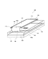
- FIG. 1 is a partially exploded perspective view showing the arrangement of the liquid crystal display module and the main substrate of the electronic device according to the first embodiment of the present invention
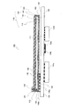
- FIG. 2 is a liquid crystal display module and the main substrate included in the electronic device. It is a fragmentary sectional view showing.
- the electronic device 100 shown in FIG. 1 is a portable terminal such as a cellular phone provided with a liquid crystal display unit 110 including a liquid crystal display module.
- the main substrate 130 and the liquid crystal display unit 110 connected to the main substrate 130 via the FPC 140 are disposed in the casing 102 in a stacked state via the protective sheet 150.
- Main substrate 130 is a printed circuit board, and is electrically connected to FPC 140 at a planar connection portion disposed on one surface (hereinafter referred to as surface) 132 facing the liquid crystal display unit in the main body portion which is an insulating plate. ing.
- a planar connection portion such as a pad provided on the front surface 133 side of the main substrate 130 is on the back surface 133 side of the main substrate 130 via a through hole or the like penetrating the main substrate portion of the main substrate 130. It is connected to the wiring part (illustration omitted) provided in.
- connection portion provided on the surface 132 side is connected by surface contact via the ACF 160 with the connection terminal portion 142 (see FIG. 1) formed at one end of the FPC 140. That is, the liquid crystal display unit 110 and the main substrate 130 are connected without using a connector, and the connection portion formed by the connection portion of the main substrate 130, the ACF 160, and the connection terminal portion 142 of the FPC 140 has a planar shape and height. Is as low as possible.
- the FPC 140 has a connection terminal portion 142 at the end of the one end portion 140 a disposed between the liquid crystal display unit 110 and the main substrate 130, and extends from the one end portion 140 a in one direction along the main substrate 130.
- the exit 140b side is folded back.
- the FPC 140 is connected to the liquid crystal display unit 110 at an end (other end) 144 of the folded back extension 140b.
- the liquid crystal display unit 110 has a liquid crystal main body provided with a plurality of liquid crystal cells sandwiched by glass, a liquid crystal drive unit, and a planar liquid crystal display module 112 whose one surface is a display surface 111; And a back light module 120 which is attached to the other surface side (rear surface) of the liquid crystal display module 112.
- the liquid crystal display module 112 has a rectangular plate shape, and light is irradiated by surface light emission of the backlight module 120 disposed opposite to the other surface (rear surface) side opposite to the display surface 111.
- the backlight module 120 includes a surface light emitting unit 122 including a rectangular light guide plate disposed on the back surface of the liquid crystal display module 112 so as to cover an effective display area of the liquid crystal display module 112, and a liquid crystal display together with the surface light emitting unit 122. It has a backlight frame portion 124 holding the module 112 and a reflective sheet 126.
- the surface light emitting portion 122 is attached to the back surface of the liquid crystal display module 112 over the entire surface, and the light emitted inside from the light source such as an LED (not shown) disposed on the side end surface of the light emitting plate emitting surface light.
- the surface light is emitted by In the light emitting plate 122, the light emitting plate 122 is a diffusion sheet, two prism sheets (light collecting sheet), and a rim sheet in this order over the entire surface (surface) of the liquid crystal display module 112 facing the liquid crystal display module 112. Are stacked.
- the diffusion sheet attached to the surface of the light guide plate in the surface light emitting unit 122 transmits and diffuses the incident light, and the prism sheet makes the traveling direction of the incident light to the light emitting surface. Output according to the orthogonal direction.
- the rim sheet of the surface light emitting unit 122 is a double-sided pressure-sensitive adhesive tape having a light shielding property, and is formed so that the light emitted from the surface light emitting unit 122 irradiates the effective display area (area where an image is displayed) of the liquid crystal display module 112 It is done.
- the backlight module 120 is integrally attached to the liquid crystal display module 112 via the rim sheet.
- a reflection sheet 126 is attached to the back surface (back surface) opposite to the surface on the liquid crystal display module 112 side.
- the surface light emitting unit 122 is held together with the liquid crystal display module 112 in a state of being stacked on the surface light emitting unit 122 by the frame portion of the backlight frame unit 124 disposed around the periphery.
- the reflection sheet 126 is attached to the surface light emitting portion 122 at least at a portion corresponding to the active area of the display surface (here over the entire surface), and light coming from a direction substantially parallel to the surface to be the attachment surface is The surface is processed to reflect in the direction orthogonal to the surface. Thereby, the reflection sheet 126 reflects the light in the light guide plate from the back side of the light guide plate to the surface (light emitting surface) side of the light guide plate.
- the light source may be fixed to the end face of the light guide plate so as to illuminate the inside of the light guide plate from the end face of the light guide plate. Also.
- the light source may be attached to the frame portion of the backlight frame portion 124 so as to emit light from the end face of the light guide plate to the light guide plate.
- liquid crystal display unit 110 a liquid crystal drive circuit (not shown) of the liquid crystal display module 112 and a light source (not shown) of the back light module 112 are provided at an end (the other end of the FPC 140) 144 of the extension 140b of the FPC 140. Etc. are electrically connected.
- the extension 140b of the FPC 140 in the electronic device 100 is the back surface side from the edge on the display surface 111 side of the one end surface 113 on the one end surface 113 side of the liquid crystal display unit 110 (reflection It extends to the sheet 126 side and is bent so as to cover the end face 113.
- the FPC 140 is disposed in the casing 102 so as to be folded back so as to surround one end surface 113 of the liquid crystal display unit 110 on the main substrate 130.
- a protective sheet 150 is disposed between the liquid crystal display unit 110 and an end portion 140 a which is a portion interposed between the liquid crystal display unit 110 and the main substrate 130 in the FPC 140 disposed in this manner.
- the protective sheet 150 covers the step portion due to the thickness of the end portion 140 a of the FPC 140 disposed on the main substrate 130.
- the protective sheet 150 is disposed on the main substrate 130 so as to cover at least the display area portion of the reflective sheet 126 and to cover the connection portion with the FPC 140.
- the protective sheet 150 is formed in a planar shape that covers the entire surface of the area facing the liquid crystal display unit 110, and is disposed so as to cover the opposing area.
- the protective sheet 150 is attached to the main substrate side, and attached, for example, via a planar adhesive such as double-sided tape.
- the protective sheet 150 is formed of a material harder than the FPC 140, and may be formed of a flexible material such as, for example, PET (Poly Ethylene Terephthalate).
- a thermal diffusion sheet such as a graphite sheet having a thickness of 50 ⁇ m, 100 ⁇ or the like, which has high thermal conductivity and thermal diffusivity is used.
- the protective sheet 150 diffuses the heat of the main substrate 130 and the heat of the FPC 140 due to the radiation of heat during operation of the electronic components 134a to 134d and the like in the housing 102, thereby reducing the heat generation of the main substrate 130 itself. doing.
- a reflective sheet 126 constituting the back surface of the backlight module 112 having the surface light emitting unit 122 attached to the upper surface of the light guide plate via the protective sheet 150 is stacked on the main substrate 130.
- the liquid crystal display unit 110 having the reflective sheet 126 on the back surface, and the electronic component on the mounting surface 133 which is disposed with the front surface 132 facing the reflective sheet 126
- An FPC 140 connected to the surface 132 of the main substrate 130 is provided between the main substrate 130 on which the 134 a to 134 d are mounted. Further, a protective sheet 150 is provided between the reflective sheet 126 and the FPC 140.
- the reflection sheet 126 constituting the back surface which is the surface on the opposite side to the display surface 111 of the liquid crystal display unit 110 depends on the thickness of the FPC 140 formed by the connection of the FPC 140 via the ACF 160 via the protection sheet 150. It is placed on the main substrate 130 having a stepped portion.
- the reflective sheet 126 is disposed on the step portion due to the thickness of the FPC 140 which is smoothed by the thickness and the deflection of the protective sheet 150 to be laminated, and therefore, it is not damaged by the corner portion of the step portion .
- the main substrate 130 and the liquid crystal display unit 110 can be suitably stacked and arranged without affecting the function of the liquid crystal display unit 110 in the housing, and the thinness of the electronic device 100 itself Can be implemented.
- the thickness of the protective sheet 150 is substantially the same as the thickness of the FPC 140, and a notch corresponding to the shape of the portion 140a of the FPC 140 disposed on the main substrate 130 is formed in the protective sheet 150.
- a portion 140 a of the FPC 140 may be disposed in the notch. That is, the reflection of the liquid crystal display unit 110 is cut out between the liquid crystal display unit 110 and the main substrate 130 so as to be flush with the surface of the FPC 140 on the liquid crystal display unit 11 side.
- a protective sheet 150 covering the sheet 126 may be interposed.
- the protective sheet 150 is disposed on the main substrate 130 on the same plane as the FPC 140 protruding from the surface of the main substrate 130, and the surface of the FPC 140 is flush with the surface of the protective sheet 150. can do. That is, the protective sheet 150 can absorb the step due to the connection portion between the FPC 140 and the main substrate 130 at the notch portion, and the reflection of the liquid crystal display unit 110 disposed on the main substrate 130 via the protective sheet 150
- the mounting surface of the sheet 126 can be made flat. Therefore, the liquid crystal display unit 110 can be disposed on the main substrate 130 without damaging the reflective sheet 126, and the thickness and size of the housing 102 can be reduced.
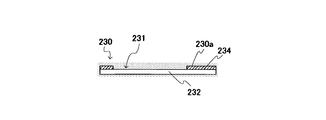
- FIG. 3 is a partial cross-sectional view showing a liquid crystal display module and a main substrate included in the electronic device according to Embodiment 2 of the present invention
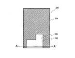
- FIG. 4 is a plan view of the main substrate of the electronic device
- FIG. It is an AA line arrow directional cross-sectional view of a substrate.
- the electronic device 200 according to the second embodiment differs from the electronic device 100 according to the first embodiment shown in FIG. 1 only in the configuration of the main substrate 230, and the other components are the same. Therefore, the same code
- the liquid crystal display unit 110 having the reflection sheet 126 on the back surface, the front surface facing the reflection sheet 126, and the electronic components 134a to 134d on the mounting surface which is the back surface.
- An FPC 140 connected on the front surface side of the main substrate 230 is provided between the mounted main substrate 230 and the main substrate 230. Further, a protective sheet 150 is provided between the reflective sheet 126 and the FPC 140.
- One surface (display surface) 230 a of the main substrate 230 included in the electronic device 200 corresponds to the end of the FPC 140 overlapped with the main substrate 230 on the surface on which the liquid crystal display unit 110 is mounted.
- the notch part 231 (refer FIG.4 and FIG.5) notched so that it may be opened to the side is provided.
- the notches 231 are applied in layers to the main substrate 230 on the side (surface) on which the liquid crystal display unit 110 is to be mounted in a rectangular plate-like base (insulation plate) 232 made of an insulating material. It is formed by cutting out the coverlay 234.
- connection terminal portion 142 connects the ACF 160 to the connection portion. It is electrically connected via
- connection portion formed by the connection terminal portion 142 of the FPC 140, the ACF 160, and the connection portion of the main substrate 230 is accommodated within the thickness range of the main substrate 230 or substantially the same as the thickness of the main substrate 230.
- the FPC 140 connected to the main substrate 230 is disposed without protruding from the surface 230 a of the main substrate 230 toward the liquid crystal display unit 110, and the surface 230 a of the main substrate 230 to which the FPC 140 is connected is substantially flat.
- a protective sheet 150 is laid on the surface 230 a side of the main substrate 230 to which the FPC 140 is connected via the ACF 160 as described above.
- the protective sheet 150 is attached to the reflective sheet 126 constituting the back surface of the liquid crystal display unit 110 so as to cover at least the effective display area on the surface of the liquid crystal display unit 110.
- the protective sheet 150 is laid over the entire surface of the overlapping area of the liquid crystal display unit 110 on the surface 230 a of the main substrate 230 (the surface on the display surface side of the liquid crystal display unit 110).
- the liquid crystal display unit 110 is stacked by sandwiching the protective sheet 150 on one surface 230 a of the main substrate 230 on which the FPC 140 electrically connected is disposed in the cutout portion 231. There is.
- the reflective sheet 126 which is the back surface of the liquid crystal display unit 110 has the FPC 140 disposed in the notch portion 231, and one surface of the substantially flat main substrate 230 (a surface on the display surface side). It arrange
- the length (thickness) in the direction perpendicular to the display surface 111 is made as short as possible in the electronic device 200 provided with the liquid crystal display unit 110. Can be made thinner.
- the cutaway portion 231 in the electronic device 200 is a portion of the cover lay 234 coated in a layer on the base material 232 where one end portion of the FPC 140 overlaps It may be cut and formed corresponding to the shape of.
- the depth of the notch 231A formed by notching the coverlay 234 in this manner is thicker than the thickness of the FPC 140.
- the surface (surface on the display surface side) of the one end portion of the FPC 140 disposed in the cutout portion 231 is substantially flush with the surface of the coverlay 234, that is, the surface 230a of the main substrate 230, or the main substrate 230 Lower than the surface 230a.
- the protective sheet is substantially flat and absorbs irregularities on the surface of the main substrate 230A without any step due to the FPC 140.
- a reflective sheet 126 is disposed via 150. Therefore, in the structure in which the liquid crystal display unit 110 is stacked on the main substrate 230A to which the FPC 140 is connected, it is possible to prevent damage to the reflective sheet 126 of the liquid crystal display unit 110 disposed overlapping on the main substrate 230.
- a notch corresponding to the shape of the portion 140a of the FPC 140 disposed in the notch portion 231 of the main substrate 230 is formed in the protective sheet 150, and a portion of the FPC 140 is formed in the notch.
- a configuration in which 140a is disposed may be used. According to this configuration, even when the FPC 140 protrudes from the surface 230 a of the main substrate 230 toward the liquid crystal display unit 110, the protruding portion is absorbed by the protective sheet 150, and the surface of the FPC 140 and the surface of the protective sheet 150 are flush with each other.
- the mounting surface of the reflective sheet 126 of the liquid crystal display unit 110 disposed on the main substrate 230 can be made flat via the protective sheet 150. Therefore, the liquid crystal display unit 110 can be disposed on the main substrate 130 without damaging the reflective sheet 126, and the thickness and size of the housing 102 can be reduced.
- the protection sheet 150 may be removed.
- FIG. 7 is a cross-sectional view of an essential part showing a configuration of an electronic device as a modification of the second embodiment according to the present invention.
- the liquid crystal display unit 110 is directly mounted on the main substrate 230 disposed in the housing 102.
- the liquid crystal display unit 110 is directly stacked on the surface of the main substrate 230 in which the FPC 140 is disposed in the cutout portion 231.
- connection portion between the main substrate 230 and the FPC 140 is flush with the surface 230 a of the main substrate 230 within the thickness range of the main substrate 230 in the notch portion 231 (see FIGS. 4 and 5). It is arranged as Further, the FPC 140 connected to the main substrate 230 at the connection portion is drawn out from the inside of the notch portion 231 and is folded back at the end portion (the other end portion of the FPC 140) 144 of the extension portion 140 b. It is connected to the site
- the FPC 140 interposed between the main substrate 230 and the liquid crystal display unit 110 is in the layer formed by the cover lay 234 on the base 232 of the main substrate 230, that is, within the thickness range of the main substrate 230, It is disposed to be substantially flush with the surface 230 a of the main substrate 230. Therefore, the liquid crystal display unit 110 directly stacked on the main substrate 230 is disposed on the substantially smooth surface 230 a of the main substrate 230.
- the thickness of the reflective portion 126 is determined by the thickness of the end 140a of the FPC 140 disposed on the main substrate 130 It is possible to cause the backlight module to perform suitable surface light emission without being damaged by the corners of the step portion.
- the same effect can be obtained even if the main substrate 230 is replaced with the main substrate 230A.
- FIG. 8 is a partially exploded perspective view showing the arrangement of the liquid crystal display module and the main substrate included in the electronic device according to the third embodiment of the present invention
- FIG. 9 is a liquid crystal display module and the main substrate included in the electronic device. It is a fragmentary sectional view shown.
- the electronic device 300 shown in FIGS. 8 and 9 further includes an FPC 340 and is different from the electronic device 100 corresponding to the first embodiment shown in FIGS.
- the electronic device 300 includes a liquid crystal display unit 110 having a reflection sheet 126 on the back surface, and a main substrate 330 on which the front surface 132 faces the reflection sheet 126 and the electronic components 134a to 134d are mounted on the mounting surface which is the back surface. Between them, the FPCs 140 and 340 connected on the surface side of the main substrate 330 are provided. In addition, a protective sheet 150 is provided between the reflective sheet 126 and the FPCs 140 and 340.
- the liquid crystal display unit 110 is disposed so as to overlap the one surface (front surface) 330a of the main substrate 330 disposed in the housing 102 with the protective sheet 150 interposed therebetween. Further, another FPC 340 is disposed between the main substrate 330 and the protective sheet 150 together with the FPC 140 connected to the liquid crystal display unit 110.
- one end 340 a is disposed along the surface 332 of the main substrate 330.
- a connection terminal 342 is formed at the end of the one end 340 a, and the connection terminal 342 is electrically connected to the connection provided on the surface 332 via the ACF 160.
- connection portion is electrically connected to the electronic components 134 a to 134 e mounted on the surface (back surface) 333 opposite to the surface 332 which is the surface on the liquid crystal display unit 110 side of the main substrate 330. That is, the main substrate 330 is a single-sided mounting substrate whose back surface side is the mounting surface 333.
- the electronic components 134a to 134d mounted on the mounting surface (back surface) 333 have a layered mold portion 335 having insulation properties. The entire surface is covered by In the same manner as in the first embodiment, connection between the connection portion provided on the surface 332 side of the main substrate 330 and the wiring portion on which the electronic components 134a to 134e are mounted on the mounting surface 333 side is through through holes or the like. Connected Each of the electronic components 134a to 134d may not cover the entire surface, and a part of each electronic component 134a to 134d may be exposed.
- the mold portion 335 is attached to the mounting surface 333 of the main substrate 330 in a state of including the electronic components 134a to 134d, and protects the electronic components 134a to 134d.
- the mold portion 335 has a flat surface which is parallel to and separated from the back surface of the main substrate 330. Note that the flat surface (also referred to as the surface) has a flat area larger than the area of the glass (glass of the liquid crystal display module 112) surface sandwiching the liquid crystal cell portion in the liquid crystal display unit 110.
- the main substrate 330 is further reinforced by the mold portion 335 and functions as one plate-like structure, and the liquid crystal display unit 110 is stacked on the surface side in the housing 102 with the protective sheet 150 interposed therebetween. And the liquid crystal display unit 110 can be supported. That is, in the electronic device 300 of the present embodiment, the same effects as those of the electronic component of the first embodiment can be obtained, and in the housing 102, a support member such as a magneframe that supports the liquid crystal display unit 110 is provided. There is no need to provide it separately, and the thickness of the electronic device 300 can be further reduced.
- the liquid crystal display unit 110 stacked on the side opposite to the surface of the mold portion 335 can be received by the surface of the mold portion 335, and the strength of the glass in the electronic device 400 can be secured.
- the protective sheet 150 is formed with a notch corresponding to the shape of the portions 140a and 340a of the FPCs 140 and 340 disposed on the main substrate 330, and one of the FPCs 140 and 340 is formed in the notch.
- the units 140a and 340 may be arranged. According to this configuration, in the electronic device 100 according to the first embodiment, the same effect as the configuration in which the protective sheet 150 is cut out can be obtained.
- FIG. 10 is a partial cross-sectional view showing the liquid crystal display module and the main substrate provided in the electronic device according to the fourth embodiment of the present invention.
- the electronic device 400 is a portable terminal such as a cellular phone provided with the liquid crystal display unit 110 including the liquid crystal display module 112 as the electronic device 100 corresponding to the first embodiment shown in FIGS. 1 and 2.
- the same components of the electronic device 400 as those of the electronic device 100 are denoted by the same reference numerals, and the description thereof is omitted.
- the electronic device 400 has the same basic configuration as the electronic device 100, and the main substrate 330 and the liquid crystal display unit 110 connected to the main substrate 430 through the FPC 140 are protected in the housing 102. It is arranged in a state of being stacked via 150.
- one ends 140a and 440a of two FPCs 140 and 440 extending in a direction away from each other along the extending direction of the main substrate 430 are connected to be separated from each other.
- the FPC 440 is the same as the other FPCs 340 in the third embodiment, and therefore the description thereof is omitted.
- the main substrate 430 is formed in a rectangular plate shape like the main substrate 130, and on the surface 430a on the side on which the liquid crystal display unit 110 is mounted, the shapes of one end portions 140a and 440a of the FPCs 140 and 440 superimposed on the main substrate 430. Notches are formed in correspondence with.
- the FPCs 140 and 440 are respectively disposed along the bottom surfaces of the cutouts in the cutouts.
- the connection terminal portions 142 and 442 in each of the FPC 140 and the other FPC 440 are connected to the connection portions disposed in the notched portion through surface contact via the ACF 160.
- the notch formed in the main substrate 430 is the surface (surface) on the side of the main substrate 430 on which the liquid crystal display unit 110 is to be placed in the rectangular plate-like base (insulation plate) 432 made of an insulating material. It is formed by cutting out the coverlay 434 applied in layers.
- connection portions respectively formed by the connection terminal portions 142 and 442 of the FPCs 140 and 440, the ACF 160, and the connection portion of the main substrate 430 are accommodated within the thickness of the main substrate 430.
- the FPCs 140 and 440 connected to the main substrate 430 do not protrude from the surface of the main substrate 430 toward the liquid crystal display unit 110, and the surface of the main substrate 230 connected to the FPCs 140 and 440 becomes substantially flat.
- the notches for housing the FPCs 140 and 440 may be formed only in the cover lay 434 applied to the base, as in the case of the main substrate 230 of the second embodiment. Further, in the main substrate 430, the thickness of the cover lay applied to the base material may be increased to form a notch for accommodating the FPCs 140 and 440.
- the liquid crystal display unit 110 is disposed on the surface side of the main substrate 430 to which the FPCs 140 and 440 are connected via the ACF 160 as described above.
- the liquid crystal display unit 110 having the reflection sheet 126 on the back surface, and the main substrate on which the front surface is disposed to face the reflection sheet 126 and the electronic components 134a to 134e are mounted on the mounting surface between them.
- FPCs 140 and 440 connected to the surface of the main substrate 430 are provided.
- a protective sheet 150 is provided between the reflective sheet 126 and the FPC 140.
- the liquid crystal display unit 110 is the same as the liquid crystal display unit 110 according to the first embodiment, and thus the description thereof is omitted.
- the protective sheet 150 in the electronic device 400 covers the connection portions of the FPCs 140 and 440 and covers at least the display area on the surface of the liquid crystal display unit 110 with respect to the reflective sheet 126 constituting the back surface of the liquid crystal display unit 110. It is attached.
- the main substrate 430 is laid over the entire surface of the portion facing the liquid crystal display unit 110.
- the main substrate 430 has a back surface as a mounting surface, like the main substrate 330 in the third embodiment, and the electronic components 134a to 134e are mounted on the mounting surface.
- the electronic components 134a to 134e are covered with a layered mold portion 435 having an insulating property.
- the mold portion 435 is attached to the main substrate 430 in a state of including the electronic components 134a to 134d, and protects the electronic components 134a to 134d.
- the mold portion 435 has a flat surface 435 a parallel to and separated from the back surface of the main substrate 430.
- the mold portion 435 is provided on one surface (back surface) which is the mounting surface, and the electronic device 400 is connected to the FPCs 140 and 440 on the surface (surface) side opposite to the mounting surface.
- the liquid crystal display unit 110 having the reflection sheet 126 on the back surface is formed on the opposite surface (surface) 430 a of the main substrate 430 by folding back the FPC 140 drawn from the surface of the main substrate 430 along the front surface. It is arrange
- the reflection sheet 126 of the liquid crystal display unit 110 is disposed on the connection portion with the FPCs 140 and 440 smoothed by the protection sheet 150 with respect to the main substrate 430, and may be damaged by the step of the connection portion. Absent.
- the main substrate 430 is further reinforced by the mold portion 435 and functions as a single plate-like structure, and the liquid crystal display unit 110 stacked on the surface side via the protective sheet 150 in the housing 102 is formed.
- the liquid crystal display unit 110 is supported.
- the same effect as the electronic component according to the first embodiment can be obtained, and in the housing 102, a support member such as a magneframe for supporting the liquid crystal display unit 110 is provided. There is no need to provide it separately, and the thickness of the electronic device 400 can be further reduced.
- the surface of mold portion 435 separated from main substrate 430 and parallel to and separated from the back surface of main substrate 430 has a flat region larger than the region of the glass surface sandwiching the liquid crystal cell portion in liquid crystal display unit 110. There is.
- the liquid crystal display unit 110 stacked on the side opposite to the surface of the mold portion can be received by the surface of the mold portion, and the strength of the glass in the electronic device 400 can be secured.
- the protection sheet 150 may have a notch having a shape corresponding to the inside of the notch of the main substrate 430, and the portions 140a and 440a of the FPCs 140 and 440 may be disposed in the notch. Good.
- the protruding portions are absorbed by the protective sheet 150, and the surfaces of the FPCs 140 and 440 and the surface of the protective sheet 150 Can be made to be That is, the mounting surface of the reflective sheet 126 of the liquid crystal display unit 110 disposed on the main substrate 430 can be flattened via the protective sheet 150, and the liquid crystal display unit 110 can be placed on the main substrate 430 without damaging the reflective sheet 126.
- the housing 102 By arranging the housing 102, the thickness and size of the housing 102 can be reduced.
- the protection sheet 150 may be removed.
- FIG. 11 is a cross-sectional view of an essential part showing a configuration of an electronic device as a modification of the fourth embodiment according to the present invention.
- the liquid crystal display unit 110 is directly mounted on the main substrate 430 disposed in the housing 102.
- the liquid crystal display unit 110 is disposed directly on the surface of the main substrate 430 on which the FPCs 140 and 440 are disposed in the notch formed by notching the cover lay 434 on the base material 432. ing.
- connection portion of the main substrate 430 and the FPCs 140 and 440 connected via the ACF 160 is disposed within the thickness range of the main substrate 430 without protruding from the surface of the main substrate 430.
- the FPCs 140 and 440 connected to the main substrate 430 at the connection portion are at the other surface of the liquid crystal display unit 110 at the other end that is drawn outward from the layer of the cover lay 434 and folded back in the notch. It is connected to the.
- the FPCs 140 and 440 interposed between the main substrate 430 and the liquid crystal display unit 110 are on the liquid crystal display unit 110 side from the surface 430 a within the thickness range of the main substrate 430 having the base material 432 and the cover lay 434. Are arranged without protruding.
- the liquid crystal display unit 110 directly stacked on the main substrate 430 is disposed on the surface of the substantially flat main substrate 430. Therefore, even if the reflective sheet 126 that constitutes the back surface of the liquid crystal display unit 110 is placed on the main substrate 430 with the FPCs 140 and 440 connected on the front side, it is formed by the thickness of the FPCs 140 and 440 on the front side of the main substrate 430 It is possible to cause the backlight module to perform suitable surface light emission without being damaged by the corner portion of the stepped portion.
- the configuration of the notched portion of the main substrate 430 may be formed by increasing the thickness of the coverlay 434 with respect to the base material 432.
- the electronic device 400A can receive the liquid crystal display unit 110 stacked on the side opposite to the surface of the mold portion on the surface 435a of the mold portion 435 in the main substrate 430.
- the strength of the glass at 400 can be secured.
- the display by the liquid crystal display module 110 is excellent.
- the thickness can be reduced while maintaining the
- the notched portion may be formed by increasing the thickness of the cover lay applied to the surface of the base in the main substrate.
- the substrate (main substrates 330 and 430) in which the mounted electronic components 134a to 134e are covered with the mold portions 335 and 435 is opposite to the mounting surface.
- the liquid crystal display unit 110 is disposed so as to overlap the side surface (surface) with the protective sheet 150 interposed therebetween.
- a liquid crystal display unit having a function similar to that of the liquid crystal display unit 110 is overlapped via a protective sheet 150 on the surface of the substrate on which the mold portions 335 and 435 are provided. You may arrange.
- the liquid crystal display unit 110 provided with the reflective sheet on the back side is disposed on the main substrate on which the protective sheet 150 is laid.
- the surface shape of the mold parts 335 and 435 is with respect to the glass surface of the liquid crystal display unit 110 to be laminated. It is formed to have a planar shape larger than the area of the glass surface of the liquid crystal display unit so that no bending force is applied.
- the ACF 140 is used for connection between the main substrate and the end of the FPC, but the present invention is not limited thereto. Any connection may be used as long as connection is made as thin as possible in the thickness of the connection portion with the end of the.
- the two may be connected by flash solder without being connected using a connector so that the thickness of the connection portion between the two is as thin as possible.
- the protective sheet 150 in each embodiment may be a radio wave absorbing sheet.
- the radio wave absorbing sheet include those formed by kneading carbon having a radio wave absorbing property, ferrite powder, various alloy powders, and the like into rubber and forming it into a sheet.
- the protective sheet 150 is a radio wave absorbing sheet, so that it comes out of the components mounted on the LCD, the substrate and the substrate. Noise and noise coming from the outside can be reduced.
- main substrates 130, 230, and 230A in electronic devices 100, 200, and 200A cover respective electronic components 134a to 134d to be mounted by a mold portion. You may do so. In this case, an effect similar to that of the electronic device 300, 400, 400A having the mold portion 335, 435 can be obtained.
- the electronic devices 200, 200A, 300, 400, and 400A can be applied to mobile terminals such as mobile phones including the liquid crystal display unit 110 having a liquid crystal display module, similarly to the electronic device 100.
- An electronic device has an effect of making it possible to reduce the thickness while maintaining good display by a liquid crystal display module, and is useful as a portable terminal device such as a mobile phone provided with a liquid crystal display unit.
Landscapes
- Physics & Mathematics (AREA)
- Engineering & Computer Science (AREA)
- Nonlinear Science (AREA)
- Signal Processing (AREA)
- Microelectronics & Electronic Packaging (AREA)
- Mathematical Physics (AREA)
- Chemical & Material Sciences (AREA)
- Crystallography & Structural Chemistry (AREA)
- General Physics & Mathematics (AREA)
- Optics & Photonics (AREA)
- Liquid Crystal (AREA)
Abstract
液晶表示ユニットによる表示を良好に保ちつつ、薄型化を図ることができる電子機器。この機器において、液晶表示ユニット(110)の背面に設けられた反射シート(126)に対向して、電子部品が実装されたメイン基板(130)が配置されている。メイン基板(130)の反射シート(126)側の面(132)には、液晶表示ユニット(110)とメイン基板(130)との間に設けられたフレキシブル基板(140)が接続されている。フレキシブル基板(140)と、反射シート(126)との間には、反射シート(126)を覆う保護シート(150)が介設されている。
Description
本発明は、液晶表示ユニットを備える電子機器に関する。
薄型ディスプレイを代表するものとして、低消費電力、軽量化、薄型化に優れる液晶ディスプレイ(液晶表示ユニットともいう)が広く用いられている。
液晶ディスプレイは、例えば、特許文献1に示すように、反射板、導光板、拡散板、輝度を向上させるプリズムシート、液晶セルの順に積層するとともに、導光板の側方に発光ダイオード(LED)等の光源とランプリフレクタを配置して構成されている。
このように構成された液晶ディスプレイが搭載された電子機器では、特許文献1に示すように、筐体内に設けられたフレームで、露出する反射板を保持したり、また、筐体に平坦部分を設け、この平坦部分に液晶ディスプレイを載置させることで、筐体内に搭載したりしている。
特開2000-200506号公報
近年、携帯電話などの携帯端末では、液晶表示ユニットを備えた構成において、更なる低消費電力化、軽量化とともに薄型化が望まれている。
これに対応して、液晶ディスプレイとメイン基板とをFPC(Flexible printed circuit)を介して接続し、メイン基板とFPCとは異方性導電フィルム(Anisotropic Conductive Film:以下、「ACF」という)を用いて接続する。そして、筐体内にメイン基板を配設し、このメイン基板にFPCを介して接続された液晶ディスプレイを、特許文献1等、従来の取付構造と同様に、フレームで保持させた状態でメイン基板上に配置することが考えられる。
このように液晶ディスプレイが取り付けられた携帯端末において、特許文献1と同様のフレームや、液晶ディスプレイを受ける平坦部材等の保持部材を用いることなく、更に筐体の厚みを薄くしたいという要望がある。
しかしながら、液晶ディスプレイを保持するフレームを無くして、筐体内の基板上に液晶ディスプレイを積層する構成では、液晶ディスプレイの背面側で露出する反射板が、メイン基板上で接続されるFPCの段差よって損傷し、液晶ディスプレイの表示面に白点現象など表示ムラができる恐れがある。
本発明の目的は、液晶表示ユニットによる表示を良好に保ちつつ、薄型化を図ることができる電子機器を提供することである。
本発明の電子機器は、反射シートを有する液晶表示ユニットと、前記反射シートに対向して配置され、前記反射シート側の面と反対側の面に電子部品が実装された基板と、前記液晶表示ユニットと前記基板との間に設けられ、前記基板に接続されるフレキシブル基板と、前記反射シートと前記フレキシブル基板との間に設けられた保護シートとを備える構成を採る。
本発明によれば、液晶表示モジュールによる表示を良好に保ちつつ、薄型化を図ることができる。
以下、本発明の実施の形態について、図面を参照して詳細に説明する。
(実施の形態1)
図1は、本発明に係る実施の形態1の電子機器の液晶表示モジュール及びメイン基板の配置状態を示す部分的分解斜視図であり、図2は、同電子機器の備える液晶表示モジュール及び メイン基板を示す部分断面図である。
図1は、本発明に係る実施の形態1の電子機器の液晶表示モジュール及びメイン基板の配置状態を示す部分的分解斜視図であり、図2は、同電子機器の備える液晶表示モジュール及び メイン基板を示す部分断面図である。
図1に示す電子機器100は、ここでは、液晶表示モジュールを含む液晶表示ユニット110を備える携帯電話機などの携帯端末である。
この電子機器100では、筐体102内に、メイン基板130と、メイン基板130にFPC140を介して接続された液晶表示ユニット110とが保護シート150を介して積層された状態で配置されている。
メイン基板130は、プリント基板であり、絶縁板である本体部分において液晶表示ユニットと対向する一方の面(以下、表面という)132に配置された面状の接続部でFPC140と電気的に接続されている。
メイン基板130の表面133側に設けられたパット等の面状の接続部(図示省略)は、メイン基板130の本体部分を貫通してなるスルーホール等を介して、メイン基板130の裏面133側に設けられた配線部分(図示省略)に接続されている。メイン基板130において、他方の面(以下、裏面という)134に配設された配線部分には、図2に示すように携帯端末100の備える機能を実現させる各電子部品134a~134dが実装されている。
メイン基板130において、表面132側に設けられた接続部は、ACF160を介してFPC140の一端部に形成された接続端子部142(図1参照)が面接触で接続されている。つまり、液晶表示ユニット110とメイン基板130とは、コネクタを用いることなく接続されており、メイン基板130の接続部、ACF160及びFPC140の接続端子部142からなる接続部分は面状をなし、高さが極力低くなっている。
FPC140は、液晶表示ユニット110とメイン基板130との間に配置された一端部140aの先端部に接続端子部142を有し、一端部140aからメイン基板130に沿って一方向に延在する延出部140b側が折り返されている。FPC140は、折り返された延出部140bの端部(他端部)144で、液晶表示ユニット110に接続されている。
液晶表示ユニット110は、ガラスに挟まれてなる複数の液晶セルを備える液晶本体、液晶駆動部を有し、一方の面を表示面111とする面状の液晶表示モジュール112と、液晶表示モジュール112の他方の面側(背面)に取り付けられ、当該液晶表示モジュール112を保持するバックライトモジュール120とを有する。
液晶表示モジュール112は、ここでは、矩形板状をなし、表示面111と反対側の面他方の面(背面)側に対向配置されたバックライトモジュール120の面発光により光が照射される。
バックライトモジュール120は、前記液晶表示モジュール112の背面に、液晶表示モジュール112における有効表示領域を覆うように配置される矩形状の導光板を含む面発光部122と、面発光部122とともに液晶表示モジュール112を保持するバックライトフレーム部124と、反射シート126とを有する。
面発光部122は、ここでは、液晶表示モジュール112の背面に、その全面に渡って取り付けられ、面発光する導光板の側端面に配置された図示しないLED等の光源から内部に照射される光により面発光する。なお、面発光部122は、導光板において、液晶表示モジュール112に対向する液晶表示モジュール112側の面(表面)の全面に渡って順に拡散シート、2枚のプリズムシート(集光シート)、リムシートを積層している。
なお、面発光部122において導光板の表面に取り付けられる拡散シートは、入射される光を透過し且つ拡散するものであり、プリズムシートは、入射された光の進行方向を、発光面に対して直交する方向に合わせて出力する。
また、面発光部122のリムシートは、遮光性を有する両面粘着テープであり、面発光部122の出射光が液晶表示モジュール112の有効表示領域(画像が表示される領域)を照射するように形成されている。これにより、バックライトモジュール120は、リムシートを介して液晶表示モジュール112に一体的に貼着されている。また、液晶表示モジュール112側の面と反対側の背面(裏面)には、反射シート126が取り付けられている。
また、面発光部122は、周囲に配置されたバックライトフレーム部124の枠部により、面発光部122上に積層された状態の液晶表示モジュール112とともに保持されている。
反射シート126は、面発光部122に、少なくとも表示面のアクティブ領域に対応する部分に(ここでは全面に渡って)貼着されて、貼着面となる表面と略平行な方向から来る光をその表面と直交する方向に反射するように表面加工が施されている。これにより、反射シート126は、導光板内の光を、導光板の背面側から導光板の表面(発光面)側に反射させるものである。なお、光源は、導光板の端面から導光板内を照射するように、導光板の端面に固定されていてもよい。また。光源は、バックライトフレーム部124における枠部に、導光板に対して当該導光板の端面から光を出射するように取り付けた構成としてもよい。
また、液晶表示ユニット110では、FPC140の延出部140bの端部(FPC140の他端部)144に、液晶表示モジュール112の液晶駆動回路(図示省略)及びバックライトモジュール112の光源(図示省略)等が電気的に接続されている。
具体的には、本実施の形態1の電子機器100におけるFPC140の延出部140bは、液晶表示ユニット110の一端面113側において、一端面113の表示面111側の縁部から背面側(反射シート126側)に延在し、一端面113を覆うように折曲されている。これにより、FPC140は、筐体102内において、メイン基板130上で、液晶表示ユニット110の一端面113を囲むように折り返された状態で配置されている。
このように配置されたFPC140において液晶表示ユニット110とメイン基板130との間に介在する部分である一端部140aと、液晶表示ユニット110との間には、保護シート150が配置されている。
保護シート150は、メイン基板130上に配置されるFPC140の端部140aの厚みによる段差部分を覆う。この保護シート150は、メイン基板130において、反射シート126において少なくとも表示エリア部分を覆うとともに、FPC140との接続部分を覆うように配置されている。本実施の形態では、保護シート150は、液晶表示ユニット110と対向する領域の全面に渡る大きさの面状に形成され、この対向する領域を覆うように配置されている。なお、保護シート150は、メイン基板側に取り付けられており、例えば、両面テープなどの面状の粘着材を介して取り付けられる。
保護シート150は、FPC140よりも硬質の材料で形成され、例えば、PET(Poly Ethylene Terephthalate)等の可撓性を有する材料により形成されてもよい。ここでは、保護シート150として、例えば、50μ、100μ等の厚みであって、熱伝導率が高く熱拡散性を有するグラファイトシート(graphite sheet)等の熱拡散シートを用いている。これにより、保護シート150は、筐体102内において、電子部品134a~134d等における動作時の熱の放射等によるメイン基板130の熱やFPC140の熱を拡散し、メイン基板130自体の発熱を軽減している。
この保護シート150を介して、導光板の上面に面発光部122が取り付けられたバックライトモジュール112の背面を構成する反射シート126が、メイン基板130上に積層されている。
このように、電子機器100では、筐体102内において、背面に反射シート126を有する液晶表示ユニット110と、表面132を反射シート126に対向して配置され、裏面である実装面133に電子部品134a~134dが実装されたメイン基板130との間に、メイン基板130の表面132に接続されたFPC140が設けられている。また、反射シート126とFPC140との間に保護シート150が設けられている。
すなわち、液晶表示ユニット110の表示面111と反対側の面である背面を構成している反射シート126は、保護シート150を介して、ACF160を介したFPC140の接続により形成されたFPC140の厚みによる段差部分を有するメイン基板130上に載置される。
これにより、反射シート126は、積層される保護シート150の厚み及び撓みによって、なだらかにされたFPC140の厚みによる段差部分上に配設されるため、当該段差部分の角部により損傷することがない。
したがって、電子機器100では筐体内において、メイン基板130と、液晶表示ユニット110とを液晶表示ユニット110の機能になんら影響を及ぼすことなく好適に重ねて配置させることができ、電子機器100自体の薄型化を図ることができる。
なお、電子機器100において、保護シート150の厚みをFPC140の厚みと略同じ厚みとし、この保護シート150に、メイン基板130上に配置されたFPC140の一部140aの形状に対応した切り欠きを形成し、この切り欠き内にFPC140の一部140aを配置した構成としてもよい。つまり、液晶表示ユニット110とメイン基板130との間には、FPC140の形状に対応して切り欠かれ、FPC140における液晶表示ユニット11側の面と面一となるように、液晶表示ユニット110の反射シート126を覆う保護シート150が介設されている構成としてもよい。
この構成によれば、保護シート150によって、メイン基板130上において、メイン基板130の表面から突出するFPC140と同一平面上に配置させて、当該FPC140の表面と保護シート150の表面とを面一にすることができる。つまり、保護シート150は、切り欠き部分で、FPC140とメイン基板130との接続部分による段差を吸収することができ、保護シート150を介してメイン基板130上に配置される液晶表示ユニット110の反射シート126の載置面を平坦にすることができる。よって、反射シート126を傷付けることなく液晶表示ユニット110をメイン基板130上に配置して、筐体102の薄型化、小型化を図ることができる。
(実施の形態2)
図3は、本発明の実施の形態2に係る電子機器の備える液晶表示モジュール及びメイン基板を示す部分断面図、図4は同電子機器のメイン基板の平面図、図5は図4に示すメイン基板のA-A線矢視断面図である。
図3は、本発明の実施の形態2に係る電子機器の備える液晶表示モジュール及びメイン基板を示す部分断面図、図4は同電子機器のメイン基板の平面図、図5は図4に示すメイン基板のA-A線矢視断面図である。
なお、この実施の形態2の電子機器200は、図1に示す実施の形態1に対応する電子機器100において、メイン基板230の構成のみ異なり、その他の構成要素は同様のものである。よって、同一の構成要素には同一の符号を付し、その説明を省略する。
すなわち、電子機器200では、筐体102内において、背面に反射シート126を有する液晶表示ユニット110と、表面を反射シート126に対向して配置され、裏面である実装面に電子部品134a~134dが実装されたメイン基板230との間に、メイン基板230の表面側で接続されたFPC140が設けられている。また、反射シート126とFPC140との間に保護シート150が設けられている。
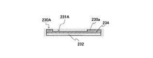
電子機器200の備えるメイン基板230には、液晶表示ユニット110が載置される側の面に、メイン基板230に重ねられるFPC140の一端部の形状に対応して、一方の面(表示面)230a側に開口するように切り欠かれた切り欠き部231(図4及び図5参照)が設けられている。
ここでは、切り欠き部231は、メイン基板230に、絶縁材からなる矩形板状の基材(絶縁板)232において液晶表示ユニット110を載置する側の面(表面)に層状に塗布されたカバーレイ234を切り欠くことで形成されている。
この切り欠き部231内には、FPC140の一端部140aに設けられた接続端子部142に接続される配線の接続部が配設されており、この接続部に、接続端子部142が、ACF160を介して電気的に接続されている。
これらFPC140の接続端子部142、ACF160及びメイン基板230の接続部とで形成される接続部分は、メイン基板230の厚みと略同等か若しくはメイン基板230の厚み範囲内に収容されている。
これによりメイン基板230に接続されるFPC140は、メイン基板230の表面230aより液晶表示ユニット110側に突出することなく配置され、FPC140を接続したメイン基板230の表面230aを略平坦面としている。
このようにFPC140がACF160を介して接続されたメイン基板230の表面230a側には、保護シート150が敷設されている。
保護シート150は、実施の形態1と同様に、液晶表示ユニット110の背面を構成する反射シート126に対して、少なくとも液晶表示ユニット110の表面における有効表示領域を覆うように取り付けられている。
ここでは、保護シート150は、メイン基板230の表面(液晶表示ユニット110の表示面側の面)230aにおいて、液晶表示ユニット110が重なる領域の全面に渡るように敷設されている。
このように電子機器220では、切り欠き部231内に、電気的に接続されたFPC140が配設されたメイン基板230の一方の面230aに、保護シート150を挟み液晶表示ユニット110が積層されている。
すなわち、液晶表示ユニット110の裏面となる反射シート126は、切り欠き部231内にFPC140が配設され、略平坦なメイン基板230の一方の面(表示面側の面、「表面」ともいう)230a上に配置された保護シート150上に配置されている。
これにより、メイン基板230上に液晶表示ユニット110を重ねることよって、液晶表示ユニット110を備える電子機器200において、表示面111と垂直な方向の長さ(厚み)を極力短くして、筐体102の薄型化を図ることができる。
なお、電子機器200における切り欠き部231は、図6に示すメイン基板230Aのように、基材232上に層状に塗布されたカバーレイ234において、FPC140の一端部が重なる部分を、その端部の形状に対応して切り欠いて形成してもよい。このようにカバーレイ234を切り欠くことで形成された切り欠き部231Aの深さは、FPC140の厚みよりも厚い。これにより、切り欠き部231内に配置されたFPC140の一端部における表面(表示面側の面)は、カバーレイ234の表面、つまり、メイン基板230の表面230aと略面一若しくは、メイン基板230の表面230aよりも低くなる。
よって、メイン基板230A上に、FPC140を挟み液晶表示ユニット110が配設された構造では、略平坦化され、FPC140による段差が無いメイン基板230Aの表面上に、表面上の凹凸を吸収する保護シート150を介して反射シート126が配置される。したがって、FPC140が接続されたメイン基板230A上に液晶表示ユニット110が積層される構造において、メイン基板230上に重ねて配置される液晶表示ユニット110の反射シート126の損傷を防止することができる。
なお、電子機器200において、保護シート150に、メイン基板230の切り欠き部231内に配置されたFPC140の一部140aの形状に対応した切り欠きを形成し、この切り欠き内にFPC140の一部140aを配置した構成としてもよい。この構成によれば、メイン基板230の表面230aからFPC140が液晶表示ユニット110側に突出する場合でも、その突出部分を保護シート150によって吸収し、FPC140の表面と保護シート150の表面とを面一にすることができる。つまり、保護シート150を介してメイン基板230上に配置される液晶表示ユニット110の反射シート126の載置面を平坦にすることができる。よって、反射シート126を傷付けることなく液晶表示ユニット110をメイン基板130上に配置して、筐体102の薄型化、小型化を図ることができる。
また、実施の形態2の電子機器200の構成において、図7に示すように、保護シート150を外した構成としてもよい。
図7は、本発明に係る実施の形態2の変形例としての電子機器の構成を示す要部断面図である。
図7に示す電子機器200Aでは、筐体102内に配設されたメイン基板230上に液晶表示ユニット110が直接載置されている。
この電子機器200Aでは、液晶表示ユニット110が、切り欠き部231内にFPC140が配設されたメイン基板230の表面上に直接、重ねて配置されている。
この構成によれば、メイン基板230とFPC140との接続部分が切り欠き部231(図4及び図5参照)内に、メイン基板230の厚み範囲内でメイン基板230の表面230aと面一となるように配設されている。また、接続部分でメイン基板230に接続されたFPC140は、切り欠き部231内から外方に導出されて折り返された延出部140bの端部(FPC140の他端部)144で液晶表示ユニット110の表面111側の部位に接続されている。
すなわち、メイン基板230と液晶表示ユニット110との間に介在するFPC140は、メイン基板230における基材232上のカバーレイ234により形成される層内、つまり、メイン基板230の厚さ範囲内に、メイン基板230の表面230aと略面一となるように配置される。よって、メイン基板230上に直接積層される液晶表示ユニット110は、略平滑なメイン基板230の表面230a上に配置されることとなる。
よって、液晶表示ユニット110の背面を構成する反射シート126は、FPC140を接続したメイン基板230の表面230a上に載置されても、メイン基板130上に配置されるFPC140の端部140aの厚みによる段差部分の角部によって損傷することがなく、バックライトモジュールに好適な面発光を行わせることができる。なお、電子機器200Aにおいて、メイン基板230をメイン基板230Aに代えても同様の効果を奏することができる。
(実施の形態3)
図8は、本発明に係る実施の形態3の電子機器が備える液晶表示モジュール及びメイン基板の配置状態を示す部分的分解斜視図、図9は、同電子機器の備える液晶表示モジュール及びメイン基板を示す部分断面図である。
図8は、本発明に係る実施の形態3の電子機器が備える液晶表示モジュール及びメイン基板の配置状態を示す部分的分解斜視図、図9は、同電子機器の備える液晶表示モジュール及びメイン基板を示す部分断面図である。
なお、図8及び図9に示す電子機器300は、図1及び図2に示す実施の形態1に対応する電子機器100と比較して、FPC340を更に備えるとともにメイン基板の構成のみ異なり、略同様の基本的構成を有している。よって、以下では、同一の構成要素には同一の符号を付し、その説明を省略する。
電子機器300は、背面に反射シート126を有する液晶表示ユニット110と、表面132を反射シート126に対向して配置され、裏面である実装面に電子部品134a~134dが実装されたメイン基板330との間に、メイン基板330の表面側で接続されたFPC140、340が設けられている。また、反射シート126とFPC140、340との間に保護シート150が設けられている。
言い換えれば、電子機器300では、筐体102内に配設されたメイン基板330の一方の面(表面)330a側に、保護シート150を介して液晶表示ユニット110が重ねて配設されている。また、これらメイン基板330と、保護シート150との間に、液晶表示ユニット110に接続されたFPC140とともに、他のFPC340が配置されている。
図9に示すように、他のFPC340は、メイン基板330の表面332に沿って一端部340aが配置されている。この一端部340aの先端には、接続端子部342が形成されており、接続端子部342は、ACF160を介して表面332に設けられた接続部に電気的に接続されている。
この接続部は、メイン基板330において液晶表示ユニット110側の面である表面332と反対側の面(裏面)333に実装された各電子部品134a~134eと電気的に接続されている。すなわち、メイン基板330は、裏面側を実装面333とした片面実装の基板であり、この実装面(裏面)333に実装された各電子部品134a~134dは、絶縁性を有する層状のモールド部335により全面を被覆されている。なお、メイン基板330において表面332側に設けられた接続部と、実装面333側において各電子部品134a~134eが実装される配線部分との接続は、実施の形態1と同様にスルーホールなどにより接続される。また、各電子部品134a~134dは、全面を被覆せず、各電子部品134a~134dの一部が露出していてもよい。
モールド部335は、メイン基板330の実装面333に各電子部品134a~134dを内包した状態で取り付けられており、各電子部品134a~134dを保護する。モールド部335は、メイン基板330の裏面と平行でかつ離間する側の面を平坦面としている。なお、平坦面(表面ともいう)は、液晶表示ユニット110において液晶セル部を挟むガラス(液晶表示モジュール112のガラス)面の領域よりも大きな平面領域を有している。
このようにメイン基板330は、モールド部335により一層補強され、一つの板状の構造体として機能し、筐体102内において、表面側で、保護シート150を介して積層された液晶表示ユニット110を受け、当該液晶表示ユニット110を支持することができる。すなわち、本実施の形態の電子機器300では、実施の形態1の電子部品と同様の効果を得ることができるとともに、筐体102内に、液晶表示ユニット110を支持するマグネフレーム等の支持部材を別途設ける必要が無く、電子機器300として更なる薄型化を図ることができる。
特に、メイン基板330では、モールド部335の表面とは反対側に積層された液晶表示ユニット110をモールド部335の表面で受けることができ、電子機器400におけるガラスの強度を確保できる。
なお、電子機器300において、保護シート150に、メイン基板330上に配置されたFPC140、340の一部140a、340aの形状に対応した切り欠きを形成し、この切り欠き内にFPC140、340の一部140a、340を配置した構成としてもよい。この構成によれば、実施の形態1の電子機器100において、保護シート150を切り欠いた構成と同様の効果を得ることができる。
(実施の形態4)
図10は本発明の実施の形態4に係る電子機器の備える液晶表示モジュール及びメイン基板を示す部分断面図である。なお、この電子機器400は、図1及び図2に示す実施の形態1に対応する電子機器100と同様に、液晶表示モジュール112を含む液晶表示ユニット110を備える携帯電話機などの携帯端末である。なお、電子機器400において電子機器100と同一の構成要素には同一の符号を付し、その説明を省略する。
図10は本発明の実施の形態4に係る電子機器の備える液晶表示モジュール及びメイン基板を示す部分断面図である。なお、この電子機器400は、図1及び図2に示す実施の形態1に対応する電子機器100と同様に、液晶表示モジュール112を含む液晶表示ユニット110を備える携帯電話機などの携帯端末である。なお、電子機器400において電子機器100と同一の構成要素には同一の符号を付し、その説明を省略する。
電子機器400は、電子機器100と同様の基本的構成を有しており、筐体102内に、メイン基板330と、メイン基板430にFPC140を介して接続された液晶表示ユニット110とが保護シート150を介して積層した状態で配置されている。
この電子機器400のメイン基板430には、メイン基板430の延在方向に沿って、互いに離間する方向に延出された2つのFPC140、440の一端部140a、440aが、互いに離間して接続されている。なお、FPC440は、実施の形態3における他のFPC340と同様のものであるため説明は省略する。
メイン基板430は、メイン基板130と同様に矩形板状に形成され、液晶表示ユニット110が載置される側の面430aに、メイン基板430に重ねられるFPC140、440の一端部140a、440aの形状に対応して切り欠き部が形成されている。これら切り欠き部内に、FPC140、440が切り欠き部の底面に沿ってそれぞれ配置されている。これらFPC140及び他のFPC440のそれぞれにおける接続端子部142、442は、切り欠き部内に配設された接続部にACF160を介して面接触にて接続されている。
ここでは、メイン基板430に形成された切り欠き部は、メイン基板430において、絶縁材からなる矩形板状の基材(絶縁板)432において液晶表示ユニット110を載置する側の面(表面)に層状に塗布されたカバーレイ434を切り欠くことで形成されている。
これらFPC140、440の接続端子部142、442、ACF160及びメイン基板430の接続部とでそれぞれ形成される接続部分は、メイン基板430の厚み内に収容されている。
これによりメイン基板430に接続されるFPC140、440は、メイン基板430の表面より液晶表示ユニット110側に突出することがなく、FPC140、440に接続されたメイン基板230の表面は、略平坦となっている。なお、メイン基板430において、FPC140、440を収容する切り欠き部は、実施の形態2のメイン基板230と同様に、基材に塗布されるカバーレイ434のみに形成されてもよい。また、メイン基板430において、基材に塗布されるカバーレイの厚みを厚くして、FPC140、440を収容する切り欠き部が形成されてもよい。
このようにACF160を介してFPC140、440がそれぞれ接続されたメイン基板430の表面側には、電子機器100と同様に、保護シート150を介して液晶表示ユニット110が配設されている。
つまり、この電子機器400では、背面に反射シート126を有する液晶表示ユニット110と、表面が反射シート126に対向して配置され、裏面である実装面に電子部品134a~134eが実装されたメイン基板430との間に、メイン基板430の表面に接続されたFPC140、440が設けられている。また、反射シート126とFPC140との間に保護シート150が設けられている。
なお、液晶表示ユニット110は、実施の形態1の液晶表示ユニット110と同様のものであるため説明を省略する。
電子機器400における保護シート150は、FPC140、440都の接続部分を覆うとともに、液晶表示ユニット110の背面を構成する反射シート126に対して、少なくとも液晶表示ユニット110の表面における表示領域を覆うように取り付けられている。ここでは、メイン基板430において、液晶表示ユニット110と対向する部位の全面渡って敷設されている。
また、メイン基板430は、実施の形態3におけるメイン基板330と同様に、裏面を実装面とし、この実装面には、各電子部品134a~134eが実装されている。これら電子部品134a~134eは、絶縁性を有する層状のモールド部435により被覆されている。
このモールド部435は、モールド部435と同様に、メイン基板430に各電子部品134a~134dを内包した状態で取り付けられており、各電子部品134a~134dを保護する。モールド部435は、実施の形態3と同様に、メイン基板430の裏面と平行でかつ離間する側の面435aを平坦面としている。
このように実施の形態4の電子機器400では、実装面である一面(裏面)に、モールド部435を有するとともに実装面とは反対の面(表面)側で、FPC140、440と接続されている。また、メイン基板430の表面から当該表面に沿って導出されたFPC140を折り返すことによって、背面に反射シート126を有する液晶表示ユニット110が、メイン基板430の反対側の面(表面)430a上に、保護シート150を介して積層された状態で配置されている。
したがって、液晶表示ユニット110の反射シート126は、メイン基板430に対して、保護シート150により平滑化されたFPC140、440との接続部分上に配置されこととなり、接続部分の段差により損傷することがない。
また、メイン基板430は、モールド部435により一層補強され、一つの板状の構造体として機能し、筐体102内において、表面側で、保護シート150を介して積層された液晶表示ユニット110を受け、当該液晶表示ユニット110を支持している。
よって、本実施の形態の電子機器400では、実施の形態1の電子部品と同様の効果を得ることができるとともに、筐体102内に、液晶表示ユニット110を支持するマグネフレーム等の支持部材を別途設ける必要が無く、電子機器400として更なる薄型化を図ることができる。
なお、モールド部435においてメイン基板430から離間するとともにメイン基板430の裏面と平行でかつ離間する表面は、液晶表示ユニット110において液晶セル部を挟むガラス面の領域よりも大きな平面領域を有している。
よって、メイン基板430では、モールド部の表面とは反対側に積層された液晶表示ユニット110をモールド部の表面で受けることができ、電子機器400におけるガラスの強度を確保できる。
なお、電子機器400において、保護シート150に、メイン基板430の切り欠き部内に対応した形状の切り欠きを形成し、この切り欠き内にFPC140、440の一部140a、440aを配置した構成としてもよい。この構成によれば、メイン基板430の表面430aからFPC140、440が液晶表示ユニット110側に突出する場合でも、その突出部分を保護シート150によって吸収し、FPC140、440の表面と保護シート150の表面とを面一にすることができる。つまり、保護シート150を介してメイン基板430上に配置される液晶表示ユニット110の反射シート126の載置面を平坦化でき、反射シート126を傷付けることなく液晶表示ユニット110をメイン基板430上に配置して、筐体102の薄型化、小型化を図ることができる。
なお、実施の形態4の電子機器400の構成において、図11に示すように、保護シート150を外した構成としてもよい。
図11は、本発明に係る実施の形態4の変形例としての電子機器の構成を示す要部断面図である。
図11に示す電子機器400Aでは、筐体102内に配設されたメイン基板430上に液晶表示ユニット110が直接載置されている。
この電子機器400Aでは、液晶表示ユニット110が、基材432上のカバーレイ434を切り欠いてなる切り欠き部内にFPC140、440が配設されたメイン基板430の表面上に直接、重ねて配置されている。
この構成によれば、メイン基板430とFPC140、440とのACF160を介して接続された接続部分がメイン基板430の厚み範囲内に、メイン基板430の表面から突出することなく配設されている。また、接続部分でメイン基板430に接続されたFPC140、440は、切り欠き部内、つまりカバーレイ434の層から外方に導出されて折り返された他端部で液晶表示ユニット110の表面側の部位に接続されている。
このように、メイン基板430と液晶表示ユニット110との間に介在するFPC140、440は、基材432とカバーレイ434とを有するメイン基板430の厚み範囲内で、表面430aから液晶表示ユニット110側に突出することなく配置されている。
これにより、メイン基板430上に直接積層される液晶表示ユニット110は、略平滑なメイン基板430の表面上に配置されることとなる。よって、液晶表示ユニット110の背面を構成する反射シート126は、表面側でFPC140、440を接続したメイン基板430上に載置されても、メイン基板430の表面側でFPC140、440の厚みにより形成される段差部分の角部によって損傷することがなく、バックライトモジュールに好適な面発光を行わせることができる。なお、電子機器400Aにおいて、メイン基板430の切り欠き部の構成は、基材432に対するカバーレイ434の厚みを大きくすることで形成してもよい。
また、電子機器400Aは、電子機器400と同様に、メイン基板430では、モールド部の表面とは反対側に積層された液晶表示ユニット110をモールド部435の表面435aで受けることができ、電子機器400におけるガラスの強度を確保できる。
このように各実施の形態の電子機器100、200,200A、300、400、400Aによれば、背面に反射シート126を備える液晶表示モジュール110を搭載した構成において、液晶表示モジュール110による表示を良好に保ちつつ、薄型化を図ることができる。
なお、本発明に係る電子機器は上記各実施の形態に限定されず、種々変更して実施することが可能である。
また、切り欠き部は、メイン基板において基材の表面に塗布されるカバーレイの厚みを厚くすることにより形成しても良い。
また、実施の形態3、4に係る電子機器300、400では、実装された電子部品134a~134eがモールド部335、435で覆われた基板(メイン基板330、430)において、実装面とは反対側の面(表面)に保護シート150を介して液晶表示ユニット110を重ねて配設した構成としている。これに加えて、各電子機器において、基板において、モールド部335、435が設けられた側の面に、液晶表示ユニット110と同様の機能を有する液晶表示ユニットを、保護シート150を介して重ねて配設してもよい。言い換えれば、背面に反射シートを備える液晶表示ユニット110は、保護シート150が敷設されたメイン基板上に重ねて配置される。なお、モールド部335、435の表面に、保護シート150を介して液晶表示ユニット110が積層される場合、モールド部335、435の表面形状は、積層される液晶表示ユニット110のガラス面に対して撓ませる力が加わらないように、液晶表示ユニットのガラス面の領域よりも大きい平面形状を有するように形成される。
また、本実施の形態に係る電子機器100、200、200A、300、400、400Aにおいて、メイン基板とFPCの端部との接続に、ACF140を用いたが、これに限らず、メイン基板とFPCの端部との接続部分の厚みが、極力薄くなるように接続するものであればどのように接続してもよい。例えば、両者の接続部分の厚みを極力薄くなるように、コネクタを用いて接続することなく、両者をフラッシュ半田により接続しても良い。
さらに、各実施の形態における保護シート150は、電波吸収シートとしてもよい。電波吸収シートとしては、電波吸収特性のあるカーボン、フェライト粉末、各種合金粉末などをゴムに練り込み、シート状に成形してなるものが挙げられる。このように各実施の形態の電子機器100、200、300、400において、保護シート150を電波吸収シートとすることにより、電子機器に悪影響を及ぼすLCDや基板及び基板に実装している部品からでるノイズや、外部から進入するノイズを軽減することができる。
なお、電子機器100、200、200Aにおけるメイン基板130、230、230Aは、実施の形態3及び4のメイン基板330、430と同様に、モールド部によって、実装される各電子部品134a~134dを覆うようにしてもよい。この場合、モールド部335、435を有する電子機器300、400、400Aと同様の効果を得ることができる。
さらに、電子機器200、200A、300、400、400Aは、電子機器100と同様に、液晶表示モジュールを有する液晶表示ユニット110を備える携帯電話機などの携帯端末に適用できる。
2007年12月28日出願の特願2007-340768の日本出願に含まれる明細書、図面および要約書の開示内容は、すべて本願に援用される。
本発明に係る電子機器は、液晶表示モジュールによる表示を良好に保ちつつ、薄型化を図ることができる発明の効果を有し、液晶表示ユニットを備える携帯電話等の携帯端末装置として有用である。
Claims (11)
- 反射シートを有する液晶表示ユニットと、
前記反射シートに対向して配置され、前記反射シート側の面と反対側の面に電子部品が実装された基板と、
前記液晶表示ユニットと前記基板との間に設けられ、前記基板に接続されるフレキシブル基板と、
前記反射シートと前記フレキシブル基板との間に設けられた保護シートと、
を備える電子機器。 - 前記保護シートは、液晶表示ユニットの表示面の表示領域と同じ表面積を有するとともに前記反射シートにおいて前記表示面の表示領域に対応した領域を覆う請求項1記載の電子機器。
- 前記基板は、前記反対側の面に、実装された前記電子部品を覆うモールド部を備える請求項1記載の電子機器。
- 前記フレキシブル基板は、接続された前記基板と前記液晶表示ユニットとの間から外方に導出され、前記液晶表示ユニットの表示面側に折曲された導出部を有し、この導出部で前記液晶表示ユニットに接続されている請求項1記載の電子機器。
- 前記保護シートは、熱拡散シートである請求項1記載の電子機器。
- 前記保護シートは、電波吸収シートである請求項1記載の電子機器。
- 前記基板は、前記反射シート側の面を形成する絶縁層を有し、
前記絶縁層には、前記液晶表示ユニットに対向する位置に配設される前記フレキシブル基板の形状に対応して形成され、前記フレキシブル基板が配設される切り欠き部が設けられている請求項1記載の電子機器。 - 前記フレキシブル基板は、前記切り欠き部内で前記基板に電気的に接続されている請求項7記載の電子機器。
- 反射シートを有する液晶表示ユニットと、
前記反射シートに対向して配置され、前記反射シート側の面と反対側の面に電子部品が実装された基板と、
前記液晶表示ユニットと前記基板との間に設けられ、前記基板に接続されるフレキシブル基板とを有し、
前記液晶表示ユニットと前記メイン基板との間には、前記フレキシブル基板の形状に対応して切り欠かれ、前記フレキシブル基板における前記液晶表示ユニット側の面と面一となるように、前記反射シートを覆う保護シートが介設されている電子機器。 - 反射シートを有する液晶表示ユニットと、
前記反射シートに対向して配置され、前記反射シート側の面を絶縁層で形成するとともに、前記反射シート側の面と反対側の面に電子部品が実装された基板と、
前記液晶表示ユニットと前記基板との間に設けられ、前記基板に接続されるフレキシブル基板とを備え、
前記絶縁層には、前記液晶表示ユニットに対向する位置に配設される前記フレキシブル基板の形状に対応して形成され、前記フレキシブル基板が配設される切り欠き部が設けられている電子機器。 - 反射シートを有する液晶表示ユニットと、
前記反射シートに対向して配置され、前記反射シート側の面と反対側の面に電子部品が実装された基板と、
前記液晶表示ユニットと前記基板との間に設けられ、前記基板に接続されるフレキシブル基板と、
前記反射シートと前記フレキシブル基板との間に設けられた保護シートと、
を備える携帯端末装置。
Priority Applications (2)
| Application Number | Priority Date | Filing Date | Title |
|---|---|---|---|
| US12/810,794 US8223294B2 (en) | 2007-12-28 | 2008-09-30 | Electronic device |
| EP08869141A EP2226675A4 (en) | 2007-12-28 | 2008-09-30 | ELECTRONIC DEVICE |
Applications Claiming Priority (2)
| Application Number | Priority Date | Filing Date | Title |
|---|---|---|---|
| JP2007340768A JP4252609B1 (ja) | 2007-12-28 | 2007-12-28 | 携帯端末装置 |
| JP2007-340768 | 2007-12-28 |
Publications (1)
| Publication Number | Publication Date |
|---|---|
| WO2009084138A1 true WO2009084138A1 (ja) | 2009-07-09 |
Family
ID=40612124
Family Applications (1)
| Application Number | Title | Priority Date | Filing Date |
|---|---|---|---|
| PCT/JP2008/002751 WO2009084138A1 (ja) | 2007-12-28 | 2008-09-30 | 電子機器 |
Country Status (4)
| Country | Link |
|---|---|
| US (1) | US8223294B2 (ja) |
| EP (1) | EP2226675A4 (ja) |
| JP (1) | JP4252609B1 (ja) |
| WO (1) | WO2009084138A1 (ja) |
Families Citing this family (6)
| Publication number | Priority date | Publication date | Assignee | Title |
|---|---|---|---|---|
| WO2011161996A1 (ja) * | 2010-06-21 | 2011-12-29 | シャープ株式会社 | 液晶表示装置 |
| JP2012184011A (ja) * | 2011-03-03 | 2012-09-27 | Asahi Glass Co Ltd | 合紙倒れ防止治具及びガラス基板梱包体 |
| JP2012242445A (ja) * | 2011-05-16 | 2012-12-10 | Sony Corp | 表示装置 |
| CN204884440U (zh) * | 2015-08-27 | 2015-12-16 | 京东方科技集团股份有限公司 | 柔性显示面板和柔性显示装置 |
| US11322489B2 (en) * | 2019-01-31 | 2022-05-03 | Innolux Corporation | Tiled display device |
| CN113380861B (zh) * | 2021-05-24 | 2023-04-18 | 云谷(固安)科技有限公司 | 显示面板及其制备方法 |
Citations (7)
| Publication number | Priority date | Publication date | Assignee | Title |
|---|---|---|---|---|
| JP2000200506A (ja) | 1998-10-28 | 2000-07-18 | Sharp Corp | バックライト |
| JP2000231096A (ja) * | 1999-02-10 | 2000-08-22 | Seiko Epson Corp | 液晶表示装置 |
| JP2002108237A (ja) * | 2000-09-29 | 2002-04-10 | Toshiba Corp | 平面表示装置 |
| JP2002148653A (ja) * | 2000-11-10 | 2002-05-22 | Citizen Watch Co Ltd | 表示装置 |
| JP2005227435A (ja) * | 2004-02-12 | 2005-08-25 | Hitachi Displays Ltd | 表示装置 |
| JP2006195296A (ja) * | 2005-01-14 | 2006-07-27 | Toshiba Matsushita Display Technology Co Ltd | 液晶表示装置 |
| JP2007212931A (ja) * | 2006-02-13 | 2007-08-23 | Citizen Holdings Co Ltd | 表示装置 |
Family Cites Families (7)
| Publication number | Priority date | Publication date | Assignee | Title |
|---|---|---|---|---|
| JP4681791B2 (ja) | 2002-08-22 | 2011-05-11 | 恵和株式会社 | 反射シート及びこれを用いたバックライトユニット |
| US6906761B2 (en) | 2001-09-19 | 2005-06-14 | Keiwa Inc. | Reflection sheet and backlight unit using the same |
| JP4594744B2 (ja) * | 2005-01-14 | 2010-12-08 | 富士通オプティカルコンポーネンツ株式会社 | 光通信デバイス及び光デバイス |
| TWI288850B (en) * | 2005-02-04 | 2007-10-21 | Chi Mei Optoelectronics Corp | Display module and flat panel display device having the same |
| JP4650624B2 (ja) * | 2005-07-27 | 2011-03-16 | 日本電気株式会社 | バックライトユニット及び液晶表示装置 |
| JP2007114325A (ja) | 2005-10-18 | 2007-05-10 | Cosmo Tec:Kk | 反射シート及び面光源装置 |
| US7952862B2 (en) * | 2008-02-22 | 2011-05-31 | Epson Imaging Devices Corporation | Electro-optical device and electronic apparatus |
-
2007
- 2007-12-28 JP JP2007340768A patent/JP4252609B1/ja not_active Expired - Fee Related
-
2008
- 2008-09-30 EP EP08869141A patent/EP2226675A4/en not_active Withdrawn
- 2008-09-30 WO PCT/JP2008/002751 patent/WO2009084138A1/ja active Application Filing
- 2008-09-30 US US12/810,794 patent/US8223294B2/en not_active Expired - Fee Related
Patent Citations (7)
| Publication number | Priority date | Publication date | Assignee | Title |
|---|---|---|---|---|
| JP2000200506A (ja) | 1998-10-28 | 2000-07-18 | Sharp Corp | バックライト |
| JP2000231096A (ja) * | 1999-02-10 | 2000-08-22 | Seiko Epson Corp | 液晶表示装置 |
| JP2002108237A (ja) * | 2000-09-29 | 2002-04-10 | Toshiba Corp | 平面表示装置 |
| JP2002148653A (ja) * | 2000-11-10 | 2002-05-22 | Citizen Watch Co Ltd | 表示装置 |
| JP2005227435A (ja) * | 2004-02-12 | 2005-08-25 | Hitachi Displays Ltd | 表示装置 |
| JP2006195296A (ja) * | 2005-01-14 | 2006-07-27 | Toshiba Matsushita Display Technology Co Ltd | 液晶表示装置 |
| JP2007212931A (ja) * | 2006-02-13 | 2007-08-23 | Citizen Holdings Co Ltd | 表示装置 |
Non-Patent Citations (1)
| Title |
|---|
| See also references of EP2226675A4 * |
Also Published As
| Publication number | Publication date |
|---|---|
| US20100279742A1 (en) | 2010-11-04 |
| US8223294B2 (en) | 2012-07-17 |
| JP4252609B1 (ja) | 2009-04-08 |
| JP2009162917A (ja) | 2009-07-23 |
| EP2226675A1 (en) | 2010-09-08 |
| EP2226675A4 (en) | 2011-07-13 |
Similar Documents
| Publication | Publication Date | Title |
|---|---|---|
| JP4622430B2 (ja) | 液晶表示装置 | |
| TWI287669B (en) | Liquid crystal display device | |
| KR101881000B1 (ko) | 디스플레이 장치의 파손 방지 구조를 구비하는 휴대용 단말기 | |
| WO2009084138A1 (ja) | 電子機器 | |
| EP3486561B1 (en) | Backlight module and display device | |
| WO2010021200A1 (ja) | 電子パッケージ、表示装置、および電子機器 | |
| JP4238921B2 (ja) | 照明装置、電気光学装置及び電子機器 | |
| TWI277796B (en) | Liquid crystal display device | |
| CN113625488A (zh) | 背光模组及显示装置 | |
| KR101121599B1 (ko) | 광원 장치 및 액정 표시 장치 | |
| CN114503064B (zh) | 显示装置及电子设备 | |
| JP4759964B2 (ja) | 液晶表示装置 | |
| US20140036539A1 (en) | Display having a separate light source | |
| CN215872067U (zh) | 电子设备 | |
| JP2005077755A (ja) | フレームケース | |
| KR101887623B1 (ko) | 인쇄회로기판 및 그를 포함하는 백라이트유닛 | |
| JP2009163249A (ja) | 電子機器 | |
| JP2010085638A (ja) | 液晶表示モジュールとこれを用いた電子機器 | |
| JP4759965B2 (ja) | 液晶表示装置 | |
| JP6975859B2 (ja) | 太陽電池ユニットおよび太陽電池ユニットを備えた無線発信機 | |
| JP2005338601A (ja) | 表示装置 | |
| JP2011095450A (ja) | 表示モジュール及び電子機器 | |
| JP4699404B2 (ja) | 携帯電子機器 | |
| KR20160135143A (ko) | 인쇄회로기판 및 그를 포함하는 백라이트유닛 | |
| KR102070639B1 (ko) | 방열회로기판, 이를 포함하는 백라이트 유닛 |
Legal Events
| Date | Code | Title | Description |
|---|---|---|---|
| 121 | Ep: the epo has been informed by wipo that ep was designated in this application |
Ref document number: 08869141 Country of ref document: EP Kind code of ref document: A1 |
|
| WWE | Wipo information: entry into national phase |
Ref document number: 2008869141 Country of ref document: EP |
|
| WWE | Wipo information: entry into national phase |
Ref document number: 12810794 Country of ref document: US |
|
| NENP | Non-entry into the national phase |
Ref country code: DE |