WO2007145229A1 - シャワープレート及びその製造方法、並びにそのシャワープレートを用いたプラズマ処理装置、プラズマ処理方法及び電子装置の製造方法 - Google Patents
シャワープレート及びその製造方法、並びにそのシャワープレートを用いたプラズマ処理装置、プラズマ処理方法及び電子装置の製造方法 Download PDFInfo
- Publication number
- WO2007145229A1 WO2007145229A1 PCT/JP2007/061857 JP2007061857W WO2007145229A1 WO 2007145229 A1 WO2007145229 A1 WO 2007145229A1 JP 2007061857 W JP2007061857 W JP 2007061857W WO 2007145229 A1 WO2007145229 A1 WO 2007145229A1
- Authority
- WO
- WIPO (PCT)
- Prior art keywords
- shower plate
- gas
- plasma
- porous
- hole
- Prior art date
- Legal status (The legal status is an assumption and is not a legal conclusion. Google has not performed a legal analysis and makes no representation as to the accuracy of the status listed.)
- Ceased
Links
Classifications
-
- B—PERFORMING OPERATIONS; TRANSPORTING
- B05—SPRAYING OR ATOMISING IN GENERAL; APPLYING FLUENT MATERIALS TO SURFACES, IN GENERAL
- B05B—SPRAYING APPARATUS; ATOMISING APPARATUS; NOZZLES
- B05B1/00—Nozzles, spray heads or other outlets, with or without auxiliary devices such as valves, heating means
- B05B1/14—Nozzles, spray heads or other outlets, with or without auxiliary devices such as valves, heating means with multiple outlet openings; with strainers in or outside the outlet opening
- B05B1/18—Roses; Shower heads
-
- C—CHEMISTRY; METALLURGY
- C23—COATING METALLIC MATERIAL; COATING MATERIAL WITH METALLIC MATERIAL; CHEMICAL SURFACE TREATMENT; DIFFUSION TREATMENT OF METALLIC MATERIAL; COATING BY VACUUM EVAPORATION, BY SPUTTERING, BY ION IMPLANTATION OR BY CHEMICAL VAPOUR DEPOSITION, IN GENERAL; INHIBITING CORROSION OF METALLIC MATERIAL OR INCRUSTATION IN GENERAL
- C23C—COATING METALLIC MATERIAL; COATING MATERIAL WITH METALLIC MATERIAL; SURFACE TREATMENT OF METALLIC MATERIAL BY DIFFUSION INTO THE SURFACE, BY CHEMICAL CONVERSION OR SUBSTITUTION; COATING BY VACUUM EVAPORATION, BY SPUTTERING, BY ION IMPLANTATION OR BY CHEMICAL VAPOUR DEPOSITION, IN GENERAL
- C23C16/00—Chemical coating by decomposition of gaseous compounds, without leaving reaction products of surface material in the coating, i.e. chemical vapour deposition [CVD] processes
- C23C16/44—Chemical coating by decomposition of gaseous compounds, without leaving reaction products of surface material in the coating, i.e. chemical vapour deposition [CVD] processes characterised by the method of coating
- C23C16/455—Chemical coating by decomposition of gaseous compounds, without leaving reaction products of surface material in the coating, i.e. chemical vapour deposition [CVD] processes characterised by the method of coating characterised by the method used for introducing gases into reaction chamber or for modifying gas flows in reaction chamber
- C23C16/45563—Gas nozzles
- C23C16/45565—Shower nozzles
-
- C—CHEMISTRY; METALLURGY
- C23—COATING METALLIC MATERIAL; COATING MATERIAL WITH METALLIC MATERIAL; CHEMICAL SURFACE TREATMENT; DIFFUSION TREATMENT OF METALLIC MATERIAL; COATING BY VACUUM EVAPORATION, BY SPUTTERING, BY ION IMPLANTATION OR BY CHEMICAL VAPOUR DEPOSITION, IN GENERAL; INHIBITING CORROSION OF METALLIC MATERIAL OR INCRUSTATION IN GENERAL
- C23C—COATING METALLIC MATERIAL; COATING MATERIAL WITH METALLIC MATERIAL; SURFACE TREATMENT OF METALLIC MATERIAL BY DIFFUSION INTO THE SURFACE, BY CHEMICAL CONVERSION OR SUBSTITUTION; COATING BY VACUUM EVAPORATION, BY SPUTTERING, BY ION IMPLANTATION OR BY CHEMICAL VAPOUR DEPOSITION, IN GENERAL
- C23C16/00—Chemical coating by decomposition of gaseous compounds, without leaving reaction products of surface material in the coating, i.e. chemical vapour deposition [CVD] processes
- C23C16/44—Chemical coating by decomposition of gaseous compounds, without leaving reaction products of surface material in the coating, i.e. chemical vapour deposition [CVD] processes characterised by the method of coating
- C23C16/455—Chemical coating by decomposition of gaseous compounds, without leaving reaction products of surface material in the coating, i.e. chemical vapour deposition [CVD] processes characterised by the method of coating characterised by the method used for introducing gases into reaction chamber or for modifying gas flows in reaction chamber
- C23C16/45563—Gas nozzles
- C23C16/45568—Porous nozzles
-
- C—CHEMISTRY; METALLURGY
- C23—COATING METALLIC MATERIAL; COATING MATERIAL WITH METALLIC MATERIAL; CHEMICAL SURFACE TREATMENT; DIFFUSION TREATMENT OF METALLIC MATERIAL; COATING BY VACUUM EVAPORATION, BY SPUTTERING, BY ION IMPLANTATION OR BY CHEMICAL VAPOUR DEPOSITION, IN GENERAL; INHIBITING CORROSION OF METALLIC MATERIAL OR INCRUSTATION IN GENERAL
- C23C—COATING METALLIC MATERIAL; COATING MATERIAL WITH METALLIC MATERIAL; SURFACE TREATMENT OF METALLIC MATERIAL BY DIFFUSION INTO THE SURFACE, BY CHEMICAL CONVERSION OR SUBSTITUTION; COATING BY VACUUM EVAPORATION, BY SPUTTERING, BY ION IMPLANTATION OR BY CHEMICAL VAPOUR DEPOSITION, IN GENERAL
- C23C16/00—Chemical coating by decomposition of gaseous compounds, without leaving reaction products of surface material in the coating, i.e. chemical vapour deposition [CVD] processes
- C23C16/44—Chemical coating by decomposition of gaseous compounds, without leaving reaction products of surface material in the coating, i.e. chemical vapour deposition [CVD] processes characterised by the method of coating
- C23C16/50—Chemical coating by decomposition of gaseous compounds, without leaving reaction products of surface material in the coating, i.e. chemical vapour deposition [CVD] processes characterised by the method of coating using electric discharges
- C23C16/511—Chemical coating by decomposition of gaseous compounds, without leaving reaction products of surface material in the coating, i.e. chemical vapour deposition [CVD] processes characterised by the method of coating using electric discharges using microwave discharges
-
- H—ELECTRICITY
- H01—ELECTRIC ELEMENTS
- H01J—ELECTRIC DISCHARGE TUBES OR DISCHARGE LAMPS
- H01J37/00—Discharge tubes with provision for introducing objects or material to be exposed to the discharge, e.g. for the purpose of examination or processing thereof
- H01J37/32—Gas-filled discharge tubes
- H01J37/32431—Constructional details of the reactor
- H01J37/3244—Gas supply means
-
- H—ELECTRICITY
- H01—ELECTRIC ELEMENTS
- H01J—ELECTRIC DISCHARGE TUBES OR DISCHARGE LAMPS
- H01J37/00—Discharge tubes with provision for introducing objects or material to be exposed to the discharge, e.g. for the purpose of examination or processing thereof
- H01J37/32—Gas-filled discharge tubes
- H01J37/32431—Constructional details of the reactor
- H01J37/3244—Gas supply means
- H01J37/32449—Gas control, e.g. control of the gas flow
Definitions
- shower plate and manufacturing method thereof and plasma processing apparatus, plasma processing method and electronic device manufacturing method using the shower plate
- the present invention relates to a plasma processing apparatus, in particular a shear plate used in a microwave plasma processing apparatus and a manufacturing method thereof, and a plasma processing apparatus, a plasma processing method and an electronic device manufacturing method using the shower plate. .
- Plasma processing steps and plasma processing apparatuses are manufacturing ultra-miniaturized semiconductor devices having a gate length of 0.1 l ⁇ m or less, which are recently called so-called deep sub-micron devices or deep sub-quarter micron devices. It is an indispensable technology for manufacturing high-resolution flat panel display devices including liquid crystal display devices.
- a microwave plasma processing apparatus that uses a high-density plasma excited by a microwave electric field without using a DC magnetic field has been proposed.
- a planar antenna having a large number of slots arranged to generate uniform microwaves (radius) A plasma processing apparatus having a configuration in which microwaves are radiated from a (line-line slot antenna) into the processing chamber and the plasma is excited by ionizing the gas in the processing chamber by the microwave electric field has been proposed (for example, Patent Document 1 reference).
- a microwave plasma excited by such a method can realize a plasma density that is wide and high directly under the antenna, and can perform uniform plasma processing in a short time.
- the microwave plasma generated by such a method excites the plasma by microwaves, damage to the substrate to be processed and metal contamination can be avoided because the electron temperature is low. Furthermore, since uniform plasma can be easily excited even on a large-area substrate, it is possible to easily cope with a manufacturing process of a semiconductor device using a large-diameter semiconductor substrate and a large-sized liquid crystal display device.
- a shower plate having a plurality of vertical holes is usually used as a gas discharge path in order to uniformly supply a plasma excitation gas into the processing chamber.
- the plasma formed directly under the shower plate may flow back into the vertical holes of the shower plate.
- abnormal discharge and gas deposition occur, which causes the problem of deterioration in the transmission efficiency and yield of microwaves for exciting the plasma.
- Patent Document 2 discloses that it is effective to make the diameter of the gas discharge hole at the tip of the vertical hole smaller than twice the sheath thickness of the plasma formed immediately below the shower plate. Yes.
- simply reducing the diameter of the gas discharge holes is not sufficient as a means for preventing the backflow of plasma.
- in order damage was the purpose of increasing the reduced processing speed, when trying to increase the plasma density from the conventional 10 12 CM_ 3 about about 10 13 CM_ 3, plasma backflow becomes remarkable, diameter of the gas discharge hole Control of the plasma alone cannot prevent plasma backflow.
- Patent Document 3 also proposes the use of a shower plate having a breathable porous ceramic sintered body strength. This is intended to prevent the backflow of plasma by the walls of a large number of pores constituting the porous ceramic sintered body.
- the shower plate which is also a general porous ceramic sintered body sintered at normal temperature and pressure, has a large variation in pore size from several ⁇ m to several tens of ⁇ m.
- the maximum crystal grain size is as large as about 20 m and the structure is not uniform, the surface flatness is poor, and if the surface in contact with the plasma is made of a porous ceramic sintered body, the effective surface area increases and the plasma is increased.
- Patent Document 3 instead of configuring the entire shower plate with a porous ceramic sintered body, an opening for gas discharge is formed in a shower plate that also has a dense alumina force, and this opening has a room temperature.
- a general porous ceramic sintered body sintered at normal pressure is mounted, and gas is released through the porous ceramic sintered body.
- a general porous ceramic sintered body sintered at normal temperature and normal pressure is used, the above-mentioned problems caused by poor surface flatness cannot be solved.
- the applicant of the present application has previously proposed a means for preventing the backflow of plasma by adjusting the diameter dimension of the gas discharge hole instead of from the structure surface of the shower plate in Patent Document 4. That is, by setting the diameter of the gas discharge hole to 0.1 to less than 0.3 mm and the tolerance of the diameter to within ⁇ 0.002 mm, the plasma backflow is prevented and the gas flow is prevented. This eliminates variation in the amount released.
- the shower plate was used in the actual microwave plasma processing apparatus under conditions with increased plasma density 10 13 CM_ 3, ⁇ this as shown FIG. 21 ⁇ This, shower plates body 600 and the cover The plasma excitation gas formed between the plate 601 and the space 602 and the vertical hole 603 communicating with the space 602 and the plasma flow back into the vertical hole 603 or the plasma excitation gas ignited in the space 602 and the vertical hole 603. Possible pale brown discoloration.
- Patent Document 1 JP-A-9-63793
- Patent Document 2 JP 2005-33167 A
- Patent Document 3 Japanese Patent Laid-Open No. 2004-39972
- Patent Document 4 Pamphlet of International Publication No. 06Z112392
- the problem to be solved by the present invention is to provide a shower plate capable of preventing plasma generation or plasma excitation gas ignition in the vertical hole portion more completely and enabling efficient plasma excitation. There is to do.
- the present invention provides a shower plate that discharges a plasma excitation gas in order to generate plasma in a plasma processing apparatus, wherein a vertical hole serving as a discharge path of the plasma excitation gas has pores communicating in the gas flow direction.
- a porous gas distribution body and a ceramic member having a plurality of gas discharge holes as appropriate are mounted, and the pore diameter of the bottleneck in the gas distribution path formed by the pores communicating with the porous gas distribution body is 10 ⁇ m.
- the pore diameter of the bottleneck of the porous gas distribution body than 10 mu m as described above it can also prevent backflow of the plasma as an increased plasma density of about 10 13 CM_ 3 It becomes. That is, in this porous gas distribution body, although the gas flowability is ensured by the connected pores, the gas flow path is bent in a zigzag shape, and is 10 / zm or less, preferably 5 m or less. Kushiro is present. On the other hand, the electrons and ions that make up the plasma have straightness! Therefore, even if the plasma flows back to the porous gas distribution body, most of the plasma collides with the pore walls, and further, all of the plasma collides in the bottleneck part of 10 m or less of the pores. Backflow is prevented.
- Patent Document 3 the use of a breathable porous ceramic sintered body as a porous gas flow medium having pores communicating in the gas flow direction in the shower plate itself is disclosed in Patent Document 3 above.
- the general porous ceramic firing used in Patent Document 3 The aggregate has a maximum crystal particle size of 20 m or more, and the pore diameter of the bottleneck in the gas flow path formed by the communicating pores is well over 10 m, so the plasma density is about 10 13 cm- 3 Under elevated conditions, plasma backflow cannot be completely prevented.
- a general porous ceramic sintered body having a relatively large crystal particle diameter has poor surface flatness, and therefore, due to the large effective surface area, the electron's ions in the plasma are regenerated. If the power efficiency of plasma excitation deteriorates, there is a problem.
- porous ceramic sintered body having a high purity that does not contain impurities that increase dielectric loss and a ceramic sintered body having a fine crystal structure and a breathable porous ceramic sintered body.
- excellent in terms of dielectric loss, strength, etc. for example, alumina-based sintered body containing high purity alumina and a small amount of grain growth inhibitor, YO and mullite, A1N
- Sintered body SiO sintered body, mullite sintered body, SiN sintered body, SiAlON sintered body etc.
- the pore size is preferably smaller than twice the thickness of the plasma sheath formed directly under the shower plate. Further, those having a fine crystal particle diameter, a uniform structure and no variation are preferable.
- the dielectric loss of the porous ceramic sintered body made of alumina-based ceramics power 1 X 10_ 3 or less, more preferably 5 X 10 _ 4 or less, the tooth forces is also a maximum crystal grain diameter of 15 m or less, more preferably 10 m or less, but the average crystal particle size is 10 m or less, more preferably 5 m or less, and the porosity is in the range of 20 to 75%, and the average pore size is 10
- the surface roughness (Ra) of the ground surface after removing the pores V should be 1.5 m or less. Can be adversely affected by the poor surface flatness of conventional porous ceramic sintered bodies and the increase in effective surface area. Can be eliminated.
- the porous ceramic sintered body having the above-mentioned characteristics is
- Such a porous gas distribution body can be disposed on the gas introduction side of the gas discharge hole provided on the gas discharge side of the vertical hole or on the tip of the vertical hole.
- the porous gas flow body if the porous gas flow body is provided on the gas introduction side of the gas discharge hole, the porous gas flow body does not directly contact the plasma, and the flatness of the lower surface of the shower plate is obstructed. Therefore, it is possible to solve the problem of the power efficiency of plasma excitation due to the increase of recombination of plasma electrons and ions.
- the characteristics such as the pressure and flow velocity of the plasma excitation gas for each vertical hole are made uniform. .
- the flow rate of the plasma excitation gas for each gas discharge hole is constant and is discharged into the plasma processing apparatus with a wide surface force of the uniform plate.
- uniform plasma can be efficiently generated directly under the shower plate.
- a porous gas distribution body having a noffer effect (buffer effect) that equalizes various characteristics such as pressure and flow velocity of the plasma excitation gas on the gas introduction side of the gas discharge hole Discharge hole force Dispersion of the flow velocity and flow rate of the released gas can be eliminated, and the generated plasma can be made uniform.
- the plasma can be prevented from flowing back to the gas introduction side of the vertical hole.
- the gas introduction side of the porous gas flow body is continuously provided with a gas passage hole having a larger diameter than the gas discharge hole. It is preferable.
- This gas passage hole serves as a path for guiding the plasma excitation gas to the porous gas distribution body side from the plasma excitation gas introduction path, which is also a horizontal hole provided in the shower plate, for example.
- the plasma excitation gas can be easily guided to the porous gas distribution body side, and the overall gas conductivity is improved. I can make it.
- the gas fluid resistance can be reduced, the gas supply pressure with less pressure loss can be set lower, which saves energy.
- the porous gas flow body can be attached to at least the tip of the longitudinal hole.
- the plasma excitation gas is released from the entire surface of the porous gas circulation body, so that the pressure of the released plasma excitation gas, Various characteristics such as flow velocity are made uniform.
- the plasma excitation gas is evenly released without variation, and it becomes possible to generate V and uniform plasma without turbulent flow directly under the shower plate.
- the shape of the porous gas flow member may be a parallel flat surface whose upper and lower surfaces are directed toward the inside of the plasma processing apparatus.
- a convex spherical shell or a concave spherical shell is preferable.
- the stress due to thermal expansion and contraction during use can be absorbed by deformation (stagnation), and cracking of the porous gas distribution body and the shower plate equipped with it can be prevented. can do.
- the plasma excitation gas can be released in a wider range, so that more uniform plasma can be generated.
- the outer periphery excluding the upper surface and the lower surface of the porous gas distribution body may be formed of a dense ceramic layer.
- the outer periphery When installing the porous gas distribution body in the vertical hole of the shower plate, the outer periphery may collapse and the particles may fall off.
- the outer periphery is collapsed by making the outer periphery a dense ceramic layer. As a result, workability is improved and contamination due to particle dropping can be prevented.
- Such a porous gas distribution body can be attached to the end of the vertical hole of the shower plate by fitting or sintering.
- the outer dimension of the porous gas distribution body is 0 to 0.002 mm relative to the inner dimension of the vertical hole of the shower plate. Fit by shrink fitting, cold fitting or press fitting.
- both the porous gas distribution body and the shower plate can be mounted at the stage before sintering, and then sintered simultaneously. That is, for the porous gas distribution body, a shower is performed at the stage of the powder molded body obtained by molding the raw material powder of the porous gas distribution body and processing it into a predetermined shape, its degreased body, pre-sintered body or sintered body.
- the porous gas circulation body is attached to the vertical holes of the shower plate, It is then sintered at the same time.
- the molding conditions or the subsequent degreasing and pre-sintering conditions are adjusted so that the shrinkage ratios of the respective members at the time of simultaneous sintering are substantially the same and at least the clamping force acts on the porous gas distribution body.
- the porous gas distribution body can be securely fixed to the vertical hole of the shower plate by mounting it at the stage before sintering and then simultaneously sintering it.
- a ceramic member having a plurality of gas discharge holes may be mounted in a vertical hole formed in a shower plate. That is, the gas discharge hole is formed in a ceramic member separate from the shutter plate, and this ceramic member is mounted in a vertical hole opened in the shower plate.
- a ceramic member having a gas discharge hole can be formed by injection molding, extrusion molding, special squeeze molding, or the like.
- the hole diameter is not more than twice the thickness of the sheath of the plasma formed immediately below the shower plate, and the length thereof is larger than the mean free path of electrons in the processing chamber. Good.
- the gas discharge side of each vertical hole is closed with the member.
- the gas discharge side of the vertical hole is narrower than the gas introduction side, and the member is provided in the narrow portion and extends to the gas introduction side.
- the gas of the member is disposed on the gas introduction side of the vertical hole.
- a porous gas flow body can also be disposed so as to be in contact with the discharge hole.
- the length of the gas discharge hole is longer than the mean free path of electrons in the plasma processing apparatus, and the hole diameter is not more than twice the thickness of the sheath of the plasma formed directly under the shower plate.
- the pore diameter of the porous body is preferably less than or equal to the thickness of the plasma formed immediately below the shower plate.
- the microwave electric field concentrates on the corner portion on the gas introduction side, so that the corner portion is chamfered.
- plasma excitation gas is supplied into the plasma processing apparatus, and the supplied plasma excitation gas is excited by microwaves to generate plasma.
- Oxidation, nitridation, oxynitridation, CVD, etching, plasma irradiation, or the like can be processed on the substrate using the plasma. The invention's effect
- the present invention it is possible to prevent the plasma from flowing back into the vertical holes that are the discharge path of the plasma excitation gas in the shower plate, and to suppress the occurrence of abnormal discharge and gas accumulation inside the shower plate. Therefore, it is possible to prevent the microwave transmission efficiency and yield deterioration for exciting the plasma.
- FIG. 1 shows a first embodiment of the present invention.
- a microwave plasma processing apparatus is shown.
- the illustrated microwave plasma processing apparatus has a processing chamber 102 that is evacuated through a plurality of exhaust ports 101, and a holding table 104 that holds a substrate to be processed 103 is disposed in the processing chamber 102.
- the processing chamber 102 A circumferentially ring-shaped space of the holding table 104 is defined, and the plurality of exhaust ports 101 are arranged at equal intervals so as to communicate with the space, that is, axially symmetric with respect to the substrate 103 to be processed. Due to the arrangement of the exhaust ports 101, the processing chamber 102 can be uniformly exhausted from the exhaust ports 101.
- An upper portion of the processing chamber 102 has a diameter force of 08 mm and a relative dielectric constant of 9.8 as a part of the outer wall of the processing chamber 102 at a position corresponding to the substrate 103 to be processed on the holding table 104. and is attached et through the low microwave dielectric loss O-ring 106 of the shower plate 105 forces the seal made of a dielectric material of alumina is (dielectric loss 1 X 10_ 3 preferably 5 X 10_ 4 below from the following) .
- a ring-shaped space 109 surrounded by two sealing O-rings 108 and the side surface of the shower plate 105 is provided at a position corresponding to the side surface of the shower plate 105 on the wall surface 107 constituting the processing chamber 102. It has been.
- the ring-shaped space 109 communicates with a gas introduction port 110 for introducing plasma excitation gas.
- a large number of lateral holes 111 having a diameter of 1 mm are opened in the lateral direction by directing force toward the center of the shower plate 105.
- a large number (230 pieces) of vertical holes 112 are opened to communicate with the processing chamber 102 so as to communicate with the horizontal holes 111.
- FIG. 2 shows the arrangement of the horizontal holes 111 and the vertical holes 112 as viewed from the upper surface of the shower plate 105.
- FIG. 3 is a schematic perspective view showing the arrangement of the horizontal holes 111 and the vertical holes 112.
- FIG. 4 shows details of the longitudinal hole 112.
- the vertical hole 112 includes a first vertical hole 112a having a diameter of 10 mm and a depth of 10 mm provided on the processing chamber 102 side, and a second vertical hole 112b having a diameter of 1 mm provided further (gas introduction side). And communicates with the lateral hole 111.
- the first vertical hole 112a has a ceramic member 113 with a height of 5mm, which is made of an extruded product of alumina and also includes a plurality of gas discharge holes 113a with a diameter of 50 ⁇ m, and a diameter of 10mm.
- a cylindrical ceramic sintered body 114 having a columnar shape with a height of 5 mm and having pores communicating in the gas flow direction is sequentially mounted.
- the second vertical hole 112b on the gas introduction side of the porous ceramic sintered body 114 corresponds to a "gas passage hole" according to claim 5 of the present application.
- a method for introducing the plasma excitation gas into the processing chamber will be described with reference to FIG.
- the plasma excitation gas introduced from the gas introduction port 110 is introduced into the ring-shaped space 109. Through the hole 111 and the vertical hole 112, the gas is finally introduced into the processing chamber 102 from the gas discharge hole 113 a provided at the tip of the vertical hole 112.
- a coaxial waveguide 117 is installed to introduce waves into the antenna.
- the slow wave plate 116 is sandwiched between the slot plate 115 and the metal plate 118.
- the metal plate 118 is provided with a cooling channel 119.
- the plasma excitation gas supplied from the shower plate 105 is ionized by microwaves radiated from the slot plate 115, so that a high density is obtained in the region of several millimeters immediately below the shower plate 105. Plasma is generated. The generated plasma reaches the substrate 103 to be processed by diffusion. From the shower plate 105, in addition to the plasma excitation gas, oxygen gas or ammonia gas may be introduced as a gas that actively generates radicals.
- a lower shower plate 120 having a conductive force such as aluminum or stainless steel is disposed between the shower plate 105 and the substrate to be processed 103 in the processing chamber 102.
- the lower shower plate 120 includes a plurality of gas flow paths 120a for introducing a process gas, which is also supplied with a process gas supply port 121, into the substrate 103 to be processed in the processing chamber 102, and the process gas is a gas flow path 120a.
- a large number of nozzles 120 b formed on the surface corresponding to the substrate to be processed 103 are discharged into the space between the lower shower plate 120 and the substrate to be processed 103.
- silane gas or disilane gas is introduced when forming a silicon-based thin film
- CF gas is introduced when forming a low dielectric constant film.
- the CVD using organometallic gas as a process gas is also possible.
- organometallic gas as a process gas
- RIE reactive ion etching
- silicon oxide film etching CF gas and acid
- Chlorine gas or HBr gas is introduced for etching of elemental gas, metal film or silicon.
- the RF power 122 is connected to the electrode installed inside the holding table 104 via a capacitor, and RF power is applied to process the self-noise voltage. Generated on the substrate 103.
- Gas type of process gas to flow Sets the gas flow and pressure by a process that is not limited to the above.
- the heat flow that flows into the shower plate 105 by being exposed to the high-density plasma is, for example, water flowing into the cooling flow path 119 via the slot plate 115, the slow wave plate 116, and the metal plate 118. Heat is exhausted by the refrigerant.
- the plurality of gas discharge holes 113a opened in the cylindrical ceramic member 113 having the alumina material force in this embodiment has a diameter of 50 / zm.
- This figure is smaller than twice the 40 m, which is the sheath thickness of 10 12 cm _3 high density plasma, but larger than twice the 10 ⁇ m, which is the sheath thickness of 10 13 c ⁇ 3 high density plasma .
- the ceramic member 113 is a dielectric loss made of 99.95% or more high-purity Al 2 O.
- V is the potential difference between the plasma and the object (unit is V)
- T is the electron temperature (unit is eV).
- ⁇ is the device length given by the following equation.
- ⁇ is the magnetic permeability in vacuum
- k is the Boltzmann constant
- n is the electron density of the plasma
- the device length decreases as the electron density of the plasma increases. From the viewpoint of preventing the backflow of the plasma, it can be said that the hole diameter of the gas discharge hole 113a is desirably smaller.
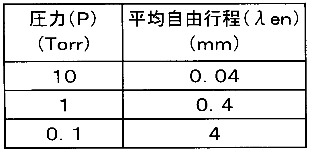
- Table 2 shows the mean free path of electrons.
- the mean free path is inversely proportional to the pressure and is 4 mm at 0.1 lTorr. Actually, the pressure on the gas inlet side of the gas discharge hole 113a is high, so the mean free path is shorter than 4mm. In this example, the length of the 50m diameter gas discharge hole 113a is 5mm and the mean free path is The value is longer than that.
- the porous ceramic sintered body 114 having pores communicating in the gas flow direction is installed on the gas introduction side of the gas discharge hole 113 3a.
- the size of the pore diameter is determined by the sheath thickness of the high-density plasma formed immediately below the shower plate 105 in order to suppress plasma from flowing back into the pores and suppressing abnormal discharge in the second vertical hole 112b. It is preferably 2 times or less, desirably less than the sheath thickness.
- Bottleneck pores i.e. gas flow path of the multi-porous ceramic sintered body 114 in this embodiment is 10 mu m Ri der less, 10 13 cm_ 3 of a sheath thickness of high-density plasma 10 / zm and below the same extent is there. By doing so, 10 13 CM_ against 3 of the high-density plasma, it is possible to use the shower plate.
- the shower plate 105 having the above configuration can prevent the plasma from flowing backward to the gas introduction side of the vertical hole 112, and can suppress the occurrence of abnormal discharge and gas accumulation inside the shower plate 105. As a result, the microwave transmission efficiency and the yield for plasma excitation can be prevented from deteriorating. In addition, efficient plasma excitation that does not hinder the flatness of the surface in contact with the plasma has become possible.
- the gas discharge hole 113a is formed by extruding into a ceramic member 113 separate from the shower plate 105 by a molding method or the like, the gas discharge hole 113a is formed when the gas discharge hole is formed in the shower plate by a hole cover. Compared to this, it is easy to form fine and long gas discharge holes with a diameter of 0.1 mm or less. I was able to do it.
- FIG. 5 shows a second embodiment of the present invention.
- a microwave plasma processing apparatus is shown.
- the same parts as those in the first embodiment are denoted by the same reference numerals and the description thereof is omitted.
- the relative permittivity is 9.8 as a part of the outer wall of the processing chamber 102 at a position corresponding to the target substrate 103 on the holding table 104 at the upper portion of the processing chamber 102.
- Teima microphone port wave dielectric loss (dielectric loss 1 X 10_ 4 below) also becomes alumina force a is the dielectric openings, i.e. plate-shaped shower longitudinal hole 200 is formed in the large number (230 pieces) Plate 201 is attached through an O-ring 106 for force sealing.
- a cover plate 202 made of alumina is provided on the upper surface side of the shower plate 201, that is, on the opposite side of the holding plate 104 with respect to the shower plate 201, and another O-ring 20 3 for sealing. It is attached via
- FIG. 6 is a schematic perspective view showing the arrangement of the shower plate 201 and the cover plate 202.
- the plasma excitation gas supply port 110 is opened in the shower plate 201 between the upper surface of the shower plate 201 and the cover plate 202.
- a space 205 for filling the plasma excitation gas supplied through the gas supply hole 204 is formed.
- the cover plate 202 is provided with grooves so as to be connected to the positions corresponding to the vertical holes 200 and the gas supply holes 204 on the surface of the cover plate 202 on the shower plate 201 side.
- a space 205 is formed between them. That is, the vertical hole 200 is disposed so as to communicate with the space 205.
- FIG. 7 shows details of the vertical hole 200.
- 7A is a sectional view
- FIG. 7B is a bottom view.
- the vertical hole 200 consists of a first vertical hole 200a having a diameter of 5 mm and a height of 2 mm from the processing chamber 102 side and a second ⁇ ⁇ 200b force having a diameter of 10 to 20 mm and a height of 8 to 20 mm.
- a cylindrical ceramic member 206 having six gas discharge holes 206a each having a diameter of 50 ⁇ m and a length of 8 mm made of alumina is formed in a part of the first and second vertical holes 200a and 200b. It is installed.
- the microwave electric field is concentrated at the corner of the vertical hole 200 on the gas introduction side to cause discharge, and the plasma excitation gas is ignited to prevent plasma from self-generating and chamfering. 2 08 is given. This chamfering is C chamfering, more preferably R chamfering, and the corner can be R chamfered after C chamfering.
- the shower plate 201 having the above-described configuration can prevent the plasma from flowing back to the gas introduction side of the vertical hole 200, and the gas for plasma excitation at the corner of the gas introduction side of the vertical hole 200 can also be prevented. No longer ignites.
- FIG. 8 shows a preferable ideal structure of the ceramic member 206.
- (A) is a cross-sectional view
- (b) is a bottom view.
- the diameter of the gas discharge holes 206a formed in the ceramic member 206 is preferably about 2 to 5 ⁇ m, and the interval is preferably about 10 to 20 ⁇ m.
- the gas release side 206 a provided in the ceramic member 206 is in contact with the gas introduction side of the ceramic member 206 having the same dimensions as in FIG.
- a porous ceramic sintered body 207 having pores communicating in the gas flow direction may be provided.
- the space portion of the second vertical hole 200b on the gas introduction side of the porous ceramic sintered body 207 corresponds to the “gas passage hole” according to claim 5 of the present application.
- the porous ceramic sintered body 207 shown in FIG. 9 of this example is an Al 2 O material having a purity of 99.9% or more, an average crystal particle diameter: L m, and a bending strength.
- L m an average crystal particle diameter
- lOOMPa For the force, a material having an average pore diameter of 3 ⁇ m, a porosity power of 5% and a thickness of 4 mm was used.
- the number, diameter, and length of the first vertical hole 200a and the second vertical hole 200b, the number, diameter, length, and the like of the gas discharge hole 206a that is opened in the ceramic member 206 are as described in this embodiment. There is no limit to the number of.
- FIG. 10 shows a third embodiment of the present invention.
- a microwave plasma processing apparatus is shown.
- the same parts as those in the first and second embodiments are denoted by the same reference numerals and the description thereof is omitted.
- the vertical hole 300 of the shower plate 301 in this embodiment has a structure as shown in FIG. That is, a gas discharge hole 300a having a diameter of 0.05 mm and a length of 0.5 mm is formed on the processing chamber 102 side where plasma is excited, and the gas introduction side of the gas discharge hole 300a is formed in a hole 300b having a diameter of lmm. It is connected.
- chamfering 303 is applied to the corner portion on the gas introduction side of the hole 300b in order to avoid electric field concentration of the microphone mouth wave.
- a porous ceramic sintered body 302 having a cylindrical shape with a height of 5 mm and pores communicating in the gas flow direction is attached to the bottom of the hole 300b having a diameter of llm.
- the gas discharge hole 300a is directly opened in the shower plate made of alumina, so it is difficult to make the length 1 mm or more, and since it is shorter than the mean free path of electrons, the electrons flow backward, and as a result.
- the plasma may be ignited in the space 205 and the vertical hole 300 and the ignition phenomenon may be continuously maintained.
- a porous ceramic sintered body 302 having the same material characteristics as that used in the second embodiment is provided on the gas introduction side of the gas discharge hole 300a.
- the numbers, diameters, lengths, and the like of the vertical holes 300, the gas discharge holes 300a, and the holes 300b are not limited to the numerical values in this embodiment.
- FIG. 12 shows a fourth embodiment of the present invention.
- a microwave plasma processing apparatus is shown. Portions that are the same as those in the first to third embodiments are given the same reference numerals and explanations thereof are omitted.
- a large number of lateral holes 401 having a diameter of lmm are showered in the lateral direction.
- the plate 400 is opened in the direction toward the center.
- a large number (230) of vertical holes 402 are opened to communicate with the processing chamber 102 so as to communicate with the horizontal holes 401.
- FIG. 13 shows the arrangement of the horizontal holes 401 and the vertical holes 402 as viewed from the upper surface of the shower plate 400.
- FIG. 14 is a schematic perspective view showing the arrangement of the horizontal holes 401 and the vertical holes 402.
- FIG. 15 shows details of the vertical hole 402.
- the vertical hole 402 has a length of about 8 to 21 mm, a diameter of 3 mm or less (preferably 1 mm or less), and a cylindrical shape with a height of about 2 to 6 mm at its tip and a pore communicating with the gas flow direction.
- a ceramic sintered body 403 is attached.
- Porous ceramics sintered body becomes alumina material strength, pore diameter of the bottleneck in the gas flow path formed by the pores communicating with the 10 m or less, the dielectric loss 1 X 10_ 3 below, the average crystal grain child size 10 m or less, porosity of 20 to 75%, average pore diameter of 10 m or less, maximum pore diameter force S75 ⁇ m or less, and bending strength of 30 MPa or more are used.
- the green body with the outer diameter, thickness, horizontal holes and vertical holes formed into the specified dimensions is sintered and relative A sintered material for shower plate having a density of 98% was obtained.
- the spray-granulated powder was fired at 800 ° C in a powder state to obtain a temporarily sintered powder, and then the shower was performed.
- the pore diameter of the bottleneck in the gas flow path formed by the connected pores is 2 m, and the dielectric loss is 2.5 X 10_ 4
- a material for sintered ceramics was obtained.
- the material for the porous ceramic sintered body the same green body as in Production Example 1 was obtained, a powder molded body obtained by processing the green body into a predetermined shape, and a degreased body obtained by firing this at 450 ° C. Further, a pre-sintered body fired at 600 ° C was prepared.
- the green body for a shower plate has a sintering shrinkage rate that varies depending on the press molding pressure, and the sintering shrinkage rate is 19% at 78 MPa and 16.2% at 147 MPa.
- the porous ceramic sintered body material changes its sintering shrinkage rate each time the porosity and pore diameter are changed, and also changes depending on the press molding pressure. Preliminarily investigate the sintering shrinkage for each characteristic setting of the sintered body
- a powder molded body, degreased body or temporary sintered body of a porous ceramic sintered body having a sintering shrinkage rate equivalent to or slightly smaller than the sintering shrinkage rate of the green body for the shower plate described above is mounted in the vertical hole. And then simultaneously sintered. As a result, a sinter bonding force is generated between them, so that a strong mounting and fixing is ensured.
- the green body for a shower plate was fired (pre-sintered) at 600-: LOOO ° C to obtain a pre-sintered body.
- pre-sintered body some sintering shrinkage occurs in the pre-sintering stage, so the residual sintering shrinkage rate when the pre-sintered body is main-sintered becomes smaller as the pre-sintering temperature becomes higher. Become.
- the porous ceramic sintered body material obtained by the same manufacturing method as in Production Example 1 and Production Example 2 uses a powder obtained by pre-sintering spray granulated powder. Dali for Sintering shrinkage is slightly smaller than that of the sintered body, and the sintering shrinkage is similar to that of the green body for shower plate, and the sintering shrinkage is similar to that of the shower plate material and porous ceramics. It is convenient to select a material for the sintered body.
- the sintering shrinkage force of the green body for the shower plate prepared in Production Example 2 was calculated, and the dimensions after sintering of the vertical holes were calculated, and the green body, degreased body, and calcined porous ceramic material were obtained.
- a porous ceramic material having a size after sintering of the sintered body and a size of the sintered body slightly larger (about 1 to 50 m) than the calculated size of the vertical hole after sintering is used for the vertical hole of the green body.
- the ceramic members (113, 206, 404) to be mounted in the vertical holes of the shower plate are also sintered together with the shower plate in the same manner as described in the above manufacturing examples 1 to 3, It can be attached to the position.
- the pore diameter of the porous ceramic sintered body 403 is desirably smaller from the viewpoint of preventing the back flow of the plasma. Specifically, it is preferable that the average pore diameter is not more than twice the plasma sheath thickness, and desirably not more than the sheath thickness. Further, the bottleneck of pores ie gas flow path of the porous ceramic sintered body 403 is less than 10 m, it is 10 13 10 m as much a sheath thickness of high-density plasma of CM_ 3 below. Thus Te cowpea to the, 10 13 CM_ against 3 of the high-density plasma, it is possible to use the shower plate
- the shower plate 400 having the above-described configuration, it is possible to prevent the plasma from flowing backward to the gas introduction side of the vertical hole 402, and abnormal discharge and gas accumulation inside the shower plate 400 can be generated. As a result, it is possible to prevent the degradation of the transmission efficiency and yield of the microphone mouth wave for exciting the plasma.
- the porous gas distribution body force mounted in the single vertical hole the plasma to be released
- the pore diameter and the air permeability are small, and when using a porous gas distribution body within the range, release is required.
- the thickness of the porous gas distribution body may be reduced to about 2-3 mm.
- a ceramic member 404 having a plurality of gas flow holes 404a may be provided in contact with the gas introduction side of the porous ceramic sintered body 403.
- Ceramic member 404 is extruded article of 99.95% or more high purity alumina (dielectric loss 1 X 10_ 3 or less), the diameter of the gas flow hole 40 4a has a diameter 50 m. This number is from 10 12 but smaller than twice the CM_ 3 high-density plasma sheet over scan a thickness 40 mu m, 10 13 2 ⁇ 10 / zm a sheath thickness of high-density plasma of CM_ 3 Is big.
- the length of the gas circulation hole 404a is 5 mm.
- the length of the gas flow hole 404a is preferably longer than the mean free path which is the mean distance until electrons are scattered.
- the mean free path is inversely proportional to the pressure and is 4 mm at 0.1 lTorr.
- the pressure on the gas inlet side of the gas circulation hole 404a is high, so that the mean free path is shorter than 4mm.
- the length of the gas discharge hole 404a is 5mm and the value is longer than the mean free path. It is said.
- another porous ceramic sintered body 403a is provided on the gas introduction side of the porous ceramic sintered body 403 instead of the ceramic member 404. It is also possible to prevent the backflow of plasma more reliably.
- the porous ceramic sintered body 403a on the gas introduction side has a larger porosity and pore diameter than the porous ceramic sintered body 403 on the gas discharge side. (For example, average pore diameter: 10 to 30 m, porosity: 50 to 75%).
- FIG. 17 shows another mounting example of the porous ceramic sintered body 403.
- a large-diameter second vertical hole 402b is provided at the tip of the first vertical hole 402a, and the porous ceramic sintered body 403 is attached to the second vertical hole 402b.
- a porous ceramics sintered body 403 is attached thereto.
- a plurality of gas flow holes 4 similar to those described in FIG. 16 (a) are provided on the gas introduction side of the porous ceramic sintered body 403.
- a ceramic member 404 in which 04a is opened is provided.
- another porous ceramic sintered body may be provided on the gas introduction side of the porous ceramic sintered body 403, as in the example of FIG. 16 (b).
- the shape of the porous ceramic sintered body 403 mounted in the second vertical hole 402b is formed so that the upper surface and the lower surface thereof are directed to the processing chamber 102 and are both concavely curved. It has a curved shape.
- the shape of the porous ceramic sintered body 403 attached to the large-diameter second vertical hole 402b provided at the tip of the first vertical hole 402a has an upper surface and a lower surface. Both are directed to the processing chamber 102 and curved into a convex curved surface.
- the porous ceramic sintered body 403 is mounted such that the lower end thereof does not protrude the lower surface force of the shower plate 400.
- a porous ceramic sintered body 403 with a curved shape As shown in Fig. 17 (b) and Fig. 17 (c), the stress due to thermal expansion and contraction when using the shower plate 400 is deformed ( It can be absorbed by stagnation), and cracking of the porous gas distribution body 403 and the shower plate 400 equipped with the porous gas distribution body 403 can be prevented.
- the plasma excitation gas when the convex surface is formed toward the processing chamber 2, the plasma excitation gas can be released in a wider range, so that more uniform plasma can be generated. It becomes.
- a ceramic member having a plurality of gas flow holes formed on the gas introduction side of the porous ceramic sintered body 403 or another porous ceramic sintered body. A body may be provided.
- the number, diameter, length, and the like of the vertical holes 112a are not limited to the numerical values in this embodiment.
- FIG. 18 shows a fifth embodiment of the present invention.
- a microwave plasma processing apparatus is shown. Portions that are the same as those in the first to fourth embodiments are assigned the same reference numerals, and descriptions thereof are omitted.
- the relative permittivity is 9.8 as a part of the outer wall of the processing chamber 102 at a position corresponding to the target substrate 103 on the holding table 104 at the upper portion of the processing chamber 102.
- Teima microphone port wave dielectric loss (dielectric loss 1 X 10_ 4 below) also becomes alumina force a is dielectric, multi A number of (230) openings, that is, plate-like shower plates with vertical holes 500 formed 501 are attached through O-rings 106 for force sealing.
- a cover plate 202 made of alumina is provided on the upper surface side of the shower plate 501, that is, on the side opposite to the holding base 10 4 with respect to the shower plate 501, and another O-ring 20 3 for sealing. It is attached via
- FIG. 19 is a schematic perspective view showing the arrangement of the shower plate 501 and the cover plate 202.
- the upper surface of the shower plate 501 and the cover plate 202 are connected via a gas supply hole 204 that is opened in the shower plate 501 from the plasma excitation gas supply port 110.
- a space 205 for filling the plasma excitation gas supplied in this way is formed.
- the cover plate 202 is provided with grooves so as to be connected to the positions corresponding to the vertical holes 500 and the gas supply holes 204 on the surface of the cover plate 202 on the shower plate 501 side.
- a space 205 is formed between them. That is, the vertical hole 500 is arranged so as to communicate with the space 205.
- FIG. 20 shows details of the vertical hole 500.
- the vertical hole 500 is composed of a first vertical hole 500a having a diameter of 8 mm and a height of 3 mm and a second vertical hole 500b having a diameter of 10 mm and a height of 7 mm from the processing chamber 102 side.
- a porous ceramic sintered body 502 having pores communicating in the gas flow direction is attached to the entire second vertical hole 500b by fitting.
- the porous ceramic sintered body 502 has an outer periphery excluding an upper surface and a lower surface formed of a dense ceramic layer 502a, and the inside is a porous portion 502b.
- the structure of the porous portion 502b is the same as that of the porous ceramic sintered body 403 of the fourth embodiment.
- Dense ceramic layer 502a has the same characteristic value and shower plate 501, specifically, the dielectric loss 1 X 10_ 3 hereinafter, the relative density Al O purity 99.95% or more Made of over 98% material.
- Such a porous ceramic sintered body 502 having the dense ceramic layer 502a on the outer periphery can be manufactured, for example, by the following method.
- first vertical hole 500a and the second vertical hole 500b are not limited to the numerical values in this example.
- the shower plate of the present invention can be used in various plasma processing apparatuses such as a microwave plasma processing apparatus, a parallel plate type high frequency excitation plasma processing apparatus, an inductively coupled plasma processing apparatus, and the like.
- FIG. 1 shows a first embodiment of the present invention.
- FIG. 2 shows the arrangement of horizontal holes and vertical holes as seen from the top surface of the shower plate shown in FIG.
- FIG. 3 shows the arrangement of the horizontal and vertical holes of the shower plate shown in FIG.
- FIG. 4 Shows details of the vertical holes in the shower plate shown in Fig. 1.
- FIG. 5 shows a second embodiment of the present invention.
- FIG. 6 Shows the arrangement of the shower plate and cover plate shown in Fig. 5.
- FIG. 7 shows details of the vertical hole of the shower plate shown in FIG.
- FIG. 8 shows a preferred ideal structure of a ceramic member to be installed in the vertical hole of the shower plate shown in FIG.
- FIG. 9 shows an example in which a porous ceramic sintered body is provided in the vertical hole of the shower plate shown in FIG.
- FIG. 10 shows a third embodiment of the present invention.
- FIG. 11 shows details of the vertical hole of the shower plate shown in FIG.
- FIG. 12 shows a fourth embodiment of the present invention.
- FIG. 13 shows the arrangement of horizontal holes and vertical holes as seen from the top surface of the shower plate shown in FIG.
- FIG. 14 shows the arrangement of the horizontal holes and vertical holes of the shower plate shown in FIG.
- FIG. 15 shows details of the vertical hole of the shower plate shown in FIG.
- FIG. 18 shows a fifth embodiment of the present invention.
- FIG. 20 shows details of the vertical hole of the shower plate shown in FIG.
- FIG. 21 Shows a conventional shower plate.
- Porous ceramic sintered body (porous gas flow body)
Landscapes
- Chemical & Material Sciences (AREA)
- Engineering & Computer Science (AREA)
- Metallurgy (AREA)
- Chemical Kinetics & Catalysis (AREA)
- Materials Engineering (AREA)
- Mechanical Engineering (AREA)
- General Chemical & Material Sciences (AREA)
- Organic Chemistry (AREA)
- Physics & Mathematics (AREA)
- Plasma & Fusion (AREA)
- Analytical Chemistry (AREA)
- Drying Of Semiconductors (AREA)
- Plasma Technology (AREA)
- Porous Artificial Stone Or Porous Ceramic Products (AREA)
- Chemical Vapour Deposition (AREA)
Abstract
Description



Claims
Priority Applications (3)
| Application Number | Priority Date | Filing Date | Title |
|---|---|---|---|
| US12/308,333 US8372200B2 (en) | 2006-06-13 | 2007-06-13 | Shower plate, method for manufacturing the shower plate, plasma processing apparatus using the shower plate, plasma processing method and electronic device manufacturing method |
| KR1020087027932A KR101130111B1 (ko) | 2006-06-13 | 2007-06-13 | 샤워 플레이트 및 그 제조 방법, 그리고 그 샤워 플레이트를 이용한 플라즈마 처리 장치, 플라즈마 처리 방법 및, 전자 장치의 제조 방법 |
| US13/729,547 US20130112337A1 (en) | 2006-06-13 | 2012-12-28 | Shower plate, manufacturing method of the shower plate, and plasma processing apparatus using the shower plate |
Applications Claiming Priority (6)
| Application Number | Priority Date | Filing Date | Title |
|---|---|---|---|
| JP2006-163357 | 2006-06-13 | ||
| JP2006163357 | 2006-06-13 | ||
| JP2006-198754 | 2006-07-20 | ||
| JP2006198754 | 2006-07-20 | ||
| JP2007153563A JP2008047869A (ja) | 2006-06-13 | 2007-06-11 | シャワープレート及びその製造方法、並びにそのシャワープレートを用いたプラズマ処理装置、プラズマ処理方法及び電子装置の製造方法 |
| JP2007-153563 | 2007-06-11 |
Related Child Applications (1)
| Application Number | Title | Priority Date | Filing Date |
|---|---|---|---|
| US13/729,547 Division US20130112337A1 (en) | 2006-06-13 | 2012-12-28 | Shower plate, manufacturing method of the shower plate, and plasma processing apparatus using the shower plate |
Publications (1)
| Publication Number | Publication Date |
|---|---|
| WO2007145229A1 true WO2007145229A1 (ja) | 2007-12-21 |
Family
ID=38831743
Family Applications (1)
| Application Number | Title | Priority Date | Filing Date |
|---|---|---|---|
| PCT/JP2007/061857 Ceased WO2007145229A1 (ja) | 2006-06-13 | 2007-06-13 | シャワープレート及びその製造方法、並びにそのシャワープレートを用いたプラズマ処理装置、プラズマ処理方法及び電子装置の製造方法 |
Country Status (6)
| Country | Link |
|---|---|
| US (2) | US8372200B2 (ja) |
| JP (1) | JP2008047869A (ja) |
| KR (1) | KR101130111B1 (ja) |
| CN (1) | CN103044063A (ja) |
| TW (1) | TWI392020B (ja) |
| WO (1) | WO2007145229A1 (ja) |
Cited By (4)
| Publication number | Priority date | Publication date | Assignee | Title |
|---|---|---|---|---|
| US20110147345A1 (en) * | 2008-05-21 | 2011-06-23 | Claus-Peter Klages | Plasma stamp, plasma treatment device, method for plasma treatment and method for producing a plasma stamp |
| KR101066173B1 (ko) | 2008-03-12 | 2011-09-20 | 고쿠리츠 다이가쿠 호진 도호쿠 다이가쿠 | 샤워 플레이트의 제조 방법, 샤워 플레이트 및 플라즈마 처리 장치 |
| JP2014120764A (ja) * | 2012-12-17 | 2014-06-30 | Gloval Material Science Co Ltd | ドライエッチング反応室チャンバの上部電極およびその製造方法 |
| CN112289673A (zh) * | 2010-10-15 | 2021-01-29 | 应用材料公司 | 用以降低在等离子体蚀刻室中的粒子缺陷的方法及设备 |
Families Citing this family (39)
| Publication number | Priority date | Publication date | Assignee | Title |
|---|---|---|---|---|
| US20080254220A1 (en) * | 2006-01-20 | 2008-10-16 | Tokyo Electron Limited | Plasma processing apparatus |
| JP2008047869A (ja) * | 2006-06-13 | 2008-02-28 | Hokuriku Seikei Kogyo Kk | シャワープレート及びその製造方法、並びにそのシャワープレートを用いたプラズマ処理装置、プラズマ処理方法及び電子装置の製造方法 |
| JP5004271B2 (ja) * | 2006-09-29 | 2012-08-22 | 東京エレクトロン株式会社 | マイクロ波プラズマ処理装置、誘電体窓の製造方法およびマイクロ波プラズマ処理方法 |
| JP5010234B2 (ja) | 2006-10-23 | 2012-08-29 | 北陸成型工業株式会社 | ガス放出孔部材を一体焼結したシャワープレートおよびその製造方法 |
| US9157152B2 (en) * | 2007-03-29 | 2015-10-13 | Tokyo Electron Limited | Vapor deposition system |
| US8673080B2 (en) | 2007-10-16 | 2014-03-18 | Novellus Systems, Inc. | Temperature controlled showerhead |
| WO2010041213A1 (en) * | 2008-10-08 | 2010-04-15 | Abcd Technology Sarl | Vapor phase deposition system |
| CN102272897A (zh) * | 2009-01-09 | 2011-12-07 | 株式会社爱发科 | 等离子体处理装置以及等离子体cvd成膜方法 |
| JP5674328B2 (ja) | 2010-03-16 | 2015-02-25 | 東京エレクトロン株式会社 | 電極及びプラズマ処理装置 |
| US8223592B2 (en) * | 2010-06-11 | 2012-07-17 | Graber Curtis E | Omni-directional acoustic radiator with radial waveguides for submersible multi-transducer array |
| EP2638959A4 (en) * | 2010-11-09 | 2015-02-11 | Samsung Electronics Co Ltd | PLASMA GENERATOR AND PLASMA PRODUCTION METHOD |
| SG192967A1 (en) | 2011-03-04 | 2013-09-30 | Novellus Systems Inc | Hybrid ceramic showerhead |
| US9111731B2 (en) * | 2011-11-29 | 2015-08-18 | Lam Research Corporation | Gas feed insert in a plasma processing chamber and methods therefor |
| US9536710B2 (en) * | 2013-02-25 | 2017-01-03 | Applied Materials, Inc. | Tunable gas delivery assembly with internal diffuser and angular injection |
| JP2015211099A (ja) * | 2014-04-25 | 2015-11-24 | 京セラ株式会社 | 真空チャック部材および真空チャック部材の製造方法。 |
| US10741365B2 (en) * | 2014-05-05 | 2020-08-11 | Lam Research Corporation | Low volume showerhead with porous baffle |
| US10378107B2 (en) | 2015-05-22 | 2019-08-13 | Lam Research Corporation | Low volume showerhead with faceplate holes for improved flow uniformity |
| US10023959B2 (en) | 2015-05-26 | 2018-07-17 | Lam Research Corporation | Anti-transient showerhead |
| JP6868616B2 (ja) * | 2015-10-08 | 2021-05-12 | アプライド マテリアルズ インコーポレイテッドApplied Materials,Incorporated | 背面でのプラズマ点火が低減されたシャワーヘッド |
| US11694911B2 (en) * | 2016-12-20 | 2023-07-04 | Lam Research Corporation | Systems and methods for metastable activated radical selective strip and etch using dual plenum showerhead |
| US10755900B2 (en) * | 2017-05-10 | 2020-08-25 | Applied Materials, Inc. | Multi-layer plasma erosion protection for chamber components |
| US10953416B2 (en) * | 2018-02-13 | 2021-03-23 | Yung-Chieh Tan | Liquid saving device |
| CN110307539A (zh) * | 2018-03-20 | 2019-10-08 | 河南神玖复合材料有限公司 | 防气体涡流燃烧装置 |
| US10903096B2 (en) * | 2018-04-06 | 2021-01-26 | Varian Semiconductor Equipment Associates, Inc. | System and apparatus for process chamber window cooling |
| US11189502B2 (en) * | 2018-04-08 | 2021-11-30 | Applied Materials, Inc. | Showerhead with interlaced gas feed and removal and methods of use |
| JP7224175B2 (ja) * | 2018-12-26 | 2023-02-17 | 東京エレクトロン株式会社 | 成膜装置及び方法 |
| CN109939618A (zh) * | 2019-03-26 | 2019-06-28 | 沈阳拓荆科技有限公司 | 喷淋结构及化学源供给系统 |
| KR20260046529A (ko) | 2019-08-23 | 2026-04-07 | 램 리써치 코포레이션 | 열 제어된 샹들리에 샤워헤드 |
| CN119980191A (zh) | 2019-08-28 | 2025-05-13 | 朗姆研究公司 | 金属沉积 |
| US11881384B2 (en) * | 2019-09-27 | 2024-01-23 | Applied Materials, Inc. | Monolithic modular microwave source with integrated process gas distribution |
| KR102695926B1 (ko) | 2019-10-07 | 2024-08-16 | 삼성전자주식회사 | 가스 공급 유닛 및 이를 포함하는 기판 처리 장치 |
| CN114929935A (zh) * | 2020-01-06 | 2022-08-19 | 朗姆研究公司 | 带有内部轮廓的面板的喷头 |
| US12131888B2 (en) * | 2020-08-31 | 2024-10-29 | Tokyo Electron Limited | Gas cluster assisted plasma processing |
| KR102748017B1 (ko) * | 2021-12-28 | 2024-12-31 | 세메스 주식회사 | 기판 처리 장치 |
| KR102895927B1 (ko) * | 2022-09-20 | 2025-12-04 | 세메스 주식회사 | 기판 처리 장치 |
| TW202431338A (zh) * | 2022-09-23 | 2024-08-01 | 美商蘭姆研究公司 | 氣體分配埠插件及包含氣體分配埠插件的設備 |
| USD1099688S1 (en) | 2022-12-09 | 2025-10-28 | Lam Research Corporation | Threaded nozzle insert |
| JP2025009849A (ja) * | 2023-06-29 | 2025-01-20 | Toto株式会社 | 静電チャック |
| CN118136485B (zh) * | 2024-05-08 | 2024-08-27 | 上海谙邦半导体设备有限公司 | 一种进气装置及等离子刻蚀机 |
Citations (10)
| Publication number | Priority date | Publication date | Assignee | Title |
|---|---|---|---|---|
| JP2001274151A (ja) * | 2000-03-24 | 2001-10-05 | Tokyo Electron Ltd | プラズマ処理装置及び方法、ガス供給リング及び誘電体 |
| JP2002299240A (ja) * | 2001-03-28 | 2002-10-11 | Tadahiro Omi | プラズマ処理装置 |
| JP2002343788A (ja) * | 2001-05-21 | 2002-11-29 | Toshiba Ceramics Co Ltd | プラズマ処理装置のガスインレット部材 |
| JP2003045809A (ja) * | 2001-07-31 | 2003-02-14 | Toshiba Ceramics Co Ltd | シャワープレート |
| JP2003332326A (ja) * | 2002-05-10 | 2003-11-21 | Tokyo Electron Ltd | プラズマ処理装置およびプラズマ処理方法 |
| JP2003338492A (ja) * | 2002-05-21 | 2003-11-28 | Tokyo Electron Ltd | プラズマ処理装置 |
| JP2004039972A (ja) * | 2002-07-05 | 2004-02-05 | Tadahiro Omi | プラズマ処理装置 |
| JP2004083362A (ja) * | 2002-08-28 | 2004-03-18 | Toshiba Ceramics Co Ltd | フッ化物セラミックス焼結体及びその製造方法 |
| JP2004228426A (ja) * | 2003-01-24 | 2004-08-12 | Mitsubishi Materials Corp | プラズマ処理装置用シャワープレートおよびその製造方法 |
| JP2005033167A (ja) * | 2003-06-19 | 2005-02-03 | Tadahiro Omi | シャワープレート、プラズマ処理装置、及び、製品の製造方法 |
Family Cites Families (52)
| Publication number | Priority date | Publication date | Assignee | Title |
|---|---|---|---|---|
| US3594011A (en) * | 1968-08-04 | 1971-07-20 | Federal Mogul Corp | Composite wear-resistant articles such as face seals |
| JPS5671575A (en) * | 1979-11-13 | 1981-06-15 | Toyoda Mach Works Ltd | Production of side plate |
| CH640571A5 (fr) * | 1981-03-06 | 1984-01-13 | Battelle Memorial Institute | Procede et dispositif pour deposer sur un substrat une couche de matiere minerale. |
| SU954106A1 (ru) * | 1981-04-21 | 1982-08-30 | Московский Ордена Ленина Авиационный Институт Им.С.Орджоникидзе | Пневматическа форсунка |
| DE69105761T2 (de) * | 1990-01-26 | 1995-08-03 | Isuzu Motors Ltd | Gusswerkstück mit keramischer Verstärkungseinlage und Verfahren zu dessen Herstellung. |
| US5962085A (en) * | 1991-02-25 | 1999-10-05 | Symetrix Corporation | Misted precursor deposition apparatus and method with improved mist and mist flow |
| US5439524A (en) * | 1993-04-05 | 1995-08-08 | Vlsi Technology, Inc. | Plasma processing apparatus |
| JPH10506150A (ja) * | 1994-08-01 | 1998-06-16 | フランツ ヘーマン、 | 非平衡軽量合金及び製品のために選択される処理 |
| JPH0963793A (ja) | 1995-08-25 | 1997-03-07 | Tokyo Electron Ltd | プラズマ処理装置 |
| US5595602A (en) * | 1995-08-14 | 1997-01-21 | Motorola, Inc. | Diffuser for uniform gas distribution in semiconductor processing and method for using the same |
| US6391690B2 (en) * | 1995-12-14 | 2002-05-21 | Seiko Epson Corporation | Thin film semiconductor device and method for producing the same |
| US6108189A (en) * | 1996-04-26 | 2000-08-22 | Applied Materials, Inc. | Electrostatic chuck having improved gas conduits |
| US5996528A (en) * | 1996-07-02 | 1999-12-07 | Novellus Systems, Inc. | Method and apparatus for flowing gases into a manifold at high potential |
| US20020011215A1 (en) * | 1997-12-12 | 2002-01-31 | Goushu Tei | Plasma treatment apparatus and method of manufacturing optical parts using the same |
| JPH11274087A (ja) * | 1998-03-25 | 1999-10-08 | Toshiba Corp | シャワープレート |
| US6182603B1 (en) * | 1998-07-13 | 2001-02-06 | Applied Komatsu Technology, Inc. | Surface-treated shower head for use in a substrate processing chamber |
| JP3595853B2 (ja) * | 1999-03-18 | 2004-12-02 | 日本エー・エス・エム株式会社 | プラズマcvd成膜装置 |
| EP1115147A4 (en) * | 1999-05-26 | 2007-05-02 | Tadahiro Ohmi | DEVICE FOR PLASMA TREATMENT |
| US6500299B1 (en) * | 1999-07-22 | 2002-12-31 | Applied Materials Inc. | Chamber having improved gas feed-through and method |
| GB9917510D0 (en) * | 1999-07-27 | 1999-09-29 | Federal Mogul Sintered Prod | Sintered steel material |
| US6502530B1 (en) * | 2000-04-26 | 2003-01-07 | Unaxis Balzers Aktiengesellschaft | Design of gas injection for the electrode in a capacitively coupled RF plasma reactor |
| US6890861B1 (en) * | 2000-06-30 | 2005-05-10 | Lam Research Corporation | Semiconductor processing equipment having improved particle performance |
| US6905079B2 (en) * | 2000-09-08 | 2005-06-14 | Tokyo Electron Limited | Shower head structure and cleaning method thereof |
| US6797639B2 (en) * | 2000-11-01 | 2004-09-28 | Applied Materials Inc. | Dielectric etch chamber with expanded process window |
| CN100418919C (zh) * | 2000-12-20 | 2008-09-17 | 株式会社村田制作所 | 透光性陶瓷及其制造方法和光学元件 |
| US6581275B2 (en) * | 2001-01-22 | 2003-06-24 | Applied Materials Inc. | Fabricating an electrostatic chuck having plasma resistant gas conduits |
| JP3904886B2 (ja) * | 2001-10-26 | 2007-04-11 | 京セラ株式会社 | シャワープレート |
| US6793733B2 (en) * | 2002-01-25 | 2004-09-21 | Applied Materials Inc. | Gas distribution showerhead |
| US7431965B2 (en) * | 2002-11-01 | 2008-10-07 | Honda Motor Co., Ltd. | Continuous growth of single-wall carbon nanotubes using chemical vapor deposition |
| US20040261712A1 (en) * | 2003-04-25 | 2004-12-30 | Daisuke Hayashi | Plasma processing apparatus |
| JP4280555B2 (ja) * | 2003-05-30 | 2009-06-17 | 東京エレクトロン株式会社 | プラズマ処理装置 |
| US6921437B1 (en) * | 2003-05-30 | 2005-07-26 | Aviza Technology, Inc. | Gas distribution system |
| KR101172334B1 (ko) * | 2003-12-26 | 2012-08-14 | 고에키자이단호진 고쿠사이카가쿠 신고우자이단 | 샤워 플레이트, 플라즈마 처리 장치, 및 제품의 제조방법 |
| US8074599B2 (en) * | 2004-05-12 | 2011-12-13 | Applied Materials, Inc. | Plasma uniformity control by gas diffuser curvature |
| JP2006186306A (ja) * | 2004-09-30 | 2006-07-13 | Toshiba Ceramics Co Ltd | ガス拡散プレートおよびその製造方法 |
| CN101176187A (zh) | 2005-04-18 | 2008-05-07 | 东京毅力科创株式会社 | 喷淋板及其制造方法 |
| US7718030B2 (en) * | 2005-09-23 | 2010-05-18 | Tokyo Electron Limited | Method and system for controlling radical distribution |
| US7638003B2 (en) * | 2006-01-12 | 2009-12-29 | Asm Japan K.K. | Semiconductor processing apparatus with lift pin structure |
| JP5068458B2 (ja) * | 2006-01-18 | 2012-11-07 | 東京エレクトロン株式会社 | プラズマ処理装置およびプラズマ処理方法 |
| US20080254220A1 (en) * | 2006-01-20 | 2008-10-16 | Tokyo Electron Limited | Plasma processing apparatus |
| JP4915985B2 (ja) * | 2006-02-06 | 2012-04-11 | 東京エレクトロン株式会社 | プラズマ処理装置およびプラズマ処理方法 |
| JP2008047869A (ja) * | 2006-06-13 | 2008-02-28 | Hokuriku Seikei Kogyo Kk | シャワープレート及びその製造方法、並びにそのシャワープレートを用いたプラズマ処理装置、プラズマ処理方法及び電子装置の製造方法 |
| JP5069427B2 (ja) * | 2006-06-13 | 2012-11-07 | 北陸成型工業株式会社 | シャワープレート、並びにそれを用いたプラズマ処理装置、プラズマ処理方法及び電子装置の製造方法 |
| JP5463536B2 (ja) * | 2006-07-20 | 2014-04-09 | 北陸成型工業株式会社 | シャワープレート及びその製造方法、並びにそのシャワープレートを用いたプラズマ処理装置、プラズマ処理方法及び電子装置の製造方法 |
| US20070062223A1 (en) * | 2006-10-16 | 2007-03-22 | Sterlite Optical Technologies Ltd | Optical fiber having reduced polarization mode dispersion (PMD) and method for producing the same |
| JP5010234B2 (ja) * | 2006-10-23 | 2012-08-29 | 北陸成型工業株式会社 | ガス放出孔部材を一体焼結したシャワープレートおよびその製造方法 |
| JP5252613B2 (ja) * | 2006-12-25 | 2013-07-31 | 国立大学法人東北大学 | イオン注入装置およびイオン注入方法 |
| US20080202814A1 (en) * | 2007-02-23 | 2008-08-28 | Lyons Nicholas J | Earth-boring tools and cutter assemblies having a cutting element co-sintered with a cone structure, methods of using the same |
| JP5058727B2 (ja) * | 2007-09-06 | 2012-10-24 | 東京エレクトロン株式会社 | 天板構造及びこれを用いたプラズマ処理装置 |
| US20090226614A1 (en) * | 2008-03-04 | 2009-09-10 | Tokyo Electron Limited | Porous gas heating device for a vapor deposition system |
| JP4590597B2 (ja) * | 2008-03-12 | 2010-12-01 | 国立大学法人東北大学 | シャワープレートの製造方法 |
| JP5396745B2 (ja) * | 2008-05-23 | 2014-01-22 | 東京エレクトロン株式会社 | プラズマ処理装置 |
-
2007
- 2007-06-11 JP JP2007153563A patent/JP2008047869A/ja active Pending
- 2007-06-13 WO PCT/JP2007/061857 patent/WO2007145229A1/ja not_active Ceased
- 2007-06-13 CN CN2012105496663A patent/CN103044063A/zh active Pending
- 2007-06-13 KR KR1020087027932A patent/KR101130111B1/ko not_active Expired - Fee Related
- 2007-06-13 TW TW096121388A patent/TWI392020B/zh not_active IP Right Cessation
- 2007-06-13 US US12/308,333 patent/US8372200B2/en not_active Expired - Fee Related
-
2012
- 2012-12-28 US US13/729,547 patent/US20130112337A1/en not_active Abandoned
Patent Citations (10)
| Publication number | Priority date | Publication date | Assignee | Title |
|---|---|---|---|---|
| JP2001274151A (ja) * | 2000-03-24 | 2001-10-05 | Tokyo Electron Ltd | プラズマ処理装置及び方法、ガス供給リング及び誘電体 |
| JP2002299240A (ja) * | 2001-03-28 | 2002-10-11 | Tadahiro Omi | プラズマ処理装置 |
| JP2002343788A (ja) * | 2001-05-21 | 2002-11-29 | Toshiba Ceramics Co Ltd | プラズマ処理装置のガスインレット部材 |
| JP2003045809A (ja) * | 2001-07-31 | 2003-02-14 | Toshiba Ceramics Co Ltd | シャワープレート |
| JP2003332326A (ja) * | 2002-05-10 | 2003-11-21 | Tokyo Electron Ltd | プラズマ処理装置およびプラズマ処理方法 |
| JP2003338492A (ja) * | 2002-05-21 | 2003-11-28 | Tokyo Electron Ltd | プラズマ処理装置 |
| JP2004039972A (ja) * | 2002-07-05 | 2004-02-05 | Tadahiro Omi | プラズマ処理装置 |
| JP2004083362A (ja) * | 2002-08-28 | 2004-03-18 | Toshiba Ceramics Co Ltd | フッ化物セラミックス焼結体及びその製造方法 |
| JP2004228426A (ja) * | 2003-01-24 | 2004-08-12 | Mitsubishi Materials Corp | プラズマ処理装置用シャワープレートおよびその製造方法 |
| JP2005033167A (ja) * | 2003-06-19 | 2005-02-03 | Tadahiro Omi | シャワープレート、プラズマ処理装置、及び、製品の製造方法 |
Cited By (7)
| Publication number | Priority date | Publication date | Assignee | Title |
|---|---|---|---|---|
| KR101066173B1 (ko) | 2008-03-12 | 2011-09-20 | 고쿠리츠 다이가쿠 호진 도호쿠 다이가쿠 | 샤워 플레이트의 제조 방법, 샤워 플레이트 및 플라즈마 처리 장치 |
| US20110147345A1 (en) * | 2008-05-21 | 2011-06-23 | Claus-Peter Klages | Plasma stamp, plasma treatment device, method for plasma treatment and method for producing a plasma stamp |
| US8904956B2 (en) * | 2008-05-21 | 2014-12-09 | Fraunhofer-Gesellschaft zur Förderung der angewandten Forschung e.V. | Plasma stamp, plasma treatment device, method for plasma treatment and method for producing a plasma stamp |
| CN112289673A (zh) * | 2010-10-15 | 2021-01-29 | 应用材料公司 | 用以降低在等离子体蚀刻室中的粒子缺陷的方法及设备 |
| US11488812B2 (en) * | 2010-10-15 | 2022-11-01 | Applied Materials, Inc. | Method and apparatus for reducing particle defects in plasma etch chambers |
| CN112289673B (zh) * | 2010-10-15 | 2024-06-25 | 应用材料公司 | 用以降低在等离子体蚀刻室中的粒子缺陷的方法及设备 |
| JP2014120764A (ja) * | 2012-12-17 | 2014-06-30 | Gloval Material Science Co Ltd | ドライエッチング反応室チャンバの上部電極およびその製造方法 |
Also Published As
| Publication number | Publication date |
|---|---|
| US8372200B2 (en) | 2013-02-12 |
| KR20080111138A (ko) | 2008-12-22 |
| US20100230387A1 (en) | 2010-09-16 |
| US20130112337A1 (en) | 2013-05-09 |
| JP2008047869A (ja) | 2008-02-28 |
| CN103044063A (zh) | 2013-04-17 |
| TWI392020B (zh) | 2013-04-01 |
| KR101130111B1 (ko) | 2012-07-05 |
| TW200828434A (en) | 2008-07-01 |
Similar Documents
| Publication | Publication Date | Title |
|---|---|---|
| WO2007145229A1 (ja) | シャワープレート及びその製造方法、並びにそのシャワープレートを用いたプラズマ処理装置、プラズマ処理方法及び電子装置の製造方法 | |
| JP5010234B2 (ja) | ガス放出孔部材を一体焼結したシャワープレートおよびその製造方法 | |
| KR101094979B1 (ko) | 샤워 플레이트 및 그 제조 방법, 그 샤워 플레이트를 이용한 플라즈마 처리 장치, 플라즈마 처리 방법 및 전자 장치의 제조 방법 | |
| JP5604622B2 (ja) | シャワープレートの製造方法 | |
| JP5069427B2 (ja) | シャワープレート、並びにそれを用いたプラズマ処理装置、プラズマ処理方法及び電子装置の製造方法 | |
| US7115184B2 (en) | Plasma processing device | |
| US20040094094A1 (en) | Plasma processing device | |
| US20090229755A1 (en) | Plasma processing apparatus | |
| JP5004271B2 (ja) | マイクロ波プラズマ処理装置、誘電体窓の製造方法およびマイクロ波プラズマ処理方法 | |
| US20080318431A1 (en) | Shower Plate and Plasma Treatment Apparatus Using Shower Plate | |
| JPH11168094A (ja) | プラズマcvd装置 | |
| CN101467498A (zh) | 喷淋板及其制造方法、和使用了它的等离子体处理装置、处理方法及电子装置的制造方法 |
Legal Events
| Date | Code | Title | Description |
|---|---|---|---|
| WWE | Wipo information: entry into national phase |
Ref document number: 200780021712.X Country of ref document: CN |
|
| 121 | Ep: the epo has been informed by wipo that ep was designated in this application |
Ref document number: 07745140 Country of ref document: EP Kind code of ref document: A1 |
|
| WWE | Wipo information: entry into national phase |
Ref document number: 1020087027932 Country of ref document: KR |
|
| WWE | Wipo information: entry into national phase |
Ref document number: 12308333 Country of ref document: US |
|
| NENP | Non-entry into the national phase |
Ref country code: DE |
|
| 122 | Ep: pct application non-entry in european phase |
Ref document number: 07745140 Country of ref document: EP Kind code of ref document: A1 |