WO2007125671A1 - 電界効果トランジスタ - Google Patents
電界効果トランジスタ Download PDFInfo
- Publication number
- WO2007125671A1 WO2007125671A1 PCT/JP2007/053092 JP2007053092W WO2007125671A1 WO 2007125671 A1 WO2007125671 A1 WO 2007125671A1 JP 2007053092 W JP2007053092 W JP 2007053092W WO 2007125671 A1 WO2007125671 A1 WO 2007125671A1
- Authority
- WO
- WIPO (PCT)
- Prior art keywords
- field effect
- group
- effect transistor
- formula
- semiconductor
- Prior art date
- Legal status (The legal status is an assumption and is not a legal conclusion. Google has not performed a legal analysis and makes no representation as to the accuracy of the status listed.)
- Ceased
Links
Classifications
-
- H—ELECTRICITY
- H10—SEMICONDUCTOR DEVICES; ELECTRIC SOLID-STATE DEVICES NOT OTHERWISE PROVIDED FOR
- H10K—ORGANIC ELECTRIC SOLID-STATE DEVICES
- H10K85/00—Organic materials used in the body or electrodes of devices covered by this subclass
- H10K85/60—Organic compounds having low molecular weight
- H10K85/649—Aromatic compounds comprising a hetero atom
- H10K85/657—Polycyclic condensed heteroaromatic hydrocarbons
- H10K85/6576—Polycyclic condensed heteroaromatic hydrocarbons comprising only sulfur in the heteroaromatic polycondensed ring system, e.g. benzothiophene
-
- H—ELECTRICITY
- H10—SEMICONDUCTOR DEVICES; ELECTRIC SOLID-STATE DEVICES NOT OTHERWISE PROVIDED FOR
- H10K—ORGANIC ELECTRIC SOLID-STATE DEVICES
- H10K10/00—Organic devices specially adapted for rectifying, amplifying, oscillating or switching; Organic capacitors or resistors having potential barriers
- H10K10/40—Organic transistors
- H10K10/46—Field-effect transistors, e.g. organic thin-film transistors [OTFT]
- H10K10/462—Insulated gate field-effect transistors [IGFETs]
- H10K10/464—Lateral top-gate IGFETs comprising only a single gate
-
- H—ELECTRICITY
- H10—SEMICONDUCTOR DEVICES; ELECTRIC SOLID-STATE DEVICES NOT OTHERWISE PROVIDED FOR
- H10K—ORGANIC ELECTRIC SOLID-STATE DEVICES
- H10K10/00—Organic devices specially adapted for rectifying, amplifying, oscillating or switching; Organic capacitors or resistors having potential barriers
- H10K10/40—Organic transistors
- H10K10/46—Field-effect transistors, e.g. organic thin-film transistors [OTFT]
- H10K10/462—Insulated gate field-effect transistors [IGFETs]
- H10K10/466—Lateral bottom-gate IGFETs comprising only a single gate
-
- H—ELECTRICITY
- H10—SEMICONDUCTOR DEVICES; ELECTRIC SOLID-STATE DEVICES NOT OTHERWISE PROVIDED FOR
- H10K—ORGANIC ELECTRIC SOLID-STATE DEVICES
- H10K10/00—Organic devices specially adapted for rectifying, amplifying, oscillating or switching; Organic capacitors or resistors having potential barriers
- H10K10/40—Organic transistors
- H10K10/46—Field-effect transistors, e.g. organic thin-film transistors [OTFT]
- H10K10/462—Insulated gate field-effect transistors [IGFETs]
- H10K10/484—Insulated gate field-effect transistors [IGFETs] characterised by the channel regions
-
- H—ELECTRICITY
- H10—SEMICONDUCTOR DEVICES; ELECTRIC SOLID-STATE DEVICES NOT OTHERWISE PROVIDED FOR
- H10K—ORGANIC ELECTRIC SOLID-STATE DEVICES
- H10K10/00—Organic devices specially adapted for rectifying, amplifying, oscillating or switching; Organic capacitors or resistors having potential barriers
- H10K10/40—Organic transistors
- H10K10/46—Field-effect transistors, e.g. organic thin-film transistors [OTFT]
- H10K10/462—Insulated gate field-effect transistors [IGFETs]
- H10K10/484—Insulated gate field-effect transistors [IGFETs] characterised by the channel regions
- H10K10/488—Insulated gate field-effect transistors [IGFETs] characterised by the channel regions the channel region comprising a layer of composite material having interpenetrating or embedded materials, e.g. a mixture of donor and acceptor moieties, that form a bulk heterojunction
Definitions
- the present invention relates to a field effect transistor. More specifically, the present invention relates to a field effect transistor having a specific organic heterocyclic compound and an electron transport semiconductor material.
- a field effect transistor generally has a structure in which a semiconductor material on a substrate is provided with a source electrode, a drain electrode, a gate electrode and the like via these electrodes and an insulator layer, and a logic circuit element.
- a semiconductor material on a substrate is provided with a source electrode, a drain electrode, a gate electrode and the like via these electrodes and an insulator layer, and a logic circuit element.
- inorganic semiconductor materials centered on silicon are used for field effect transistors, and thin film transistors made of amorphous silicon on a substrate such as glass are used for displays and the like.
- it is necessary to process the field effect transistor at a high temperature or in a vacuum, and it requires a large amount of energy for capital investment and manufacturing, so the cost becomes very high.
- substrates that are not sufficiently heat resistant such as films and plastics cannot be used as substrates because they are exposed to high temperatures during the production of field effect transistors. Is limited.
- DP h BDS compounds and DPh-BSBS compounds show excellent P-type semiconductor characteristics and are reported to be more stable, and as practical organic semiconductor materials, they can be used as organic field-effect transistors.
- Expectations are high (see Patent Document 3, Non-Patent Document 1, and Non-Patent Document 2)
- Organic semiconductor materials with electron transport (N-type) properties include fluorinated pentacene, fluorinated phthalocyanine, C60, and perylenetetracarboxylic anhydride.
- ambipolar type field effect transistors that can be driven by N-type or P-type by changing the polarity of the gate voltage on the same element are attracting attention.
- This realization makes it possible to fabricate CMOS circuits much more easily than combining the above-mentioned P-type and N-type separately, and opens the way for other applications.
- ambipolar type electric For the production of field effect transistors, the above-mentioned pentacene and fluorinated pentacene are used, and phthalocyanine and fluorinated phthalocyanine are used for lamination and mixing. 3 and Non-Patent Document 4, Non-Patent Document 4).
- an ambipolar type field effect transistor can be produced by using calcium having a low work function for an electrode using a single material.
- Patent Document 1 Japanese Patent Application Laid-Open No. 2001-94107
- Patent Document 2 JP-A-6-177380
- Patent Document 3 Japanese Patent Laid-Open No. 2005-154371
- Non-Patent Document 1 OK. AM. CHEM. SOC. 2004, 126, 5084-5085
- Non-Patent Document 2 OK. AM. CHEM. SOC. 2006, 128, 3044- 3050
- Non-Patent Document 3 OK. AM. CHEM. SOC. 2004, 126, 8138 -8140
- Non-Patent Document 4 APPL PHYS. LETT. 86, 253505 (2005)
- Non-Patent Document 5 APPL PHYS. LETT. 87, 093507 (2005)
- An object of the present invention is to provide an ambipolar field effect transistor having a practical level of charge mobility and excellent stability in the atmosphere.
- the present inventors have achieved excellent carrier mobility by using a bicyclic compound having a specific structure and an electron transport semiconductor material as constituent components.
- a field effect transistor excellent in stability was obtained, and it was found that the device exhibited unpolar characteristics, and the present invention was completed.
- the configuration of the present invention is as follows.
- X to X each independently represent a sulfur atom, a selenium atom or a tellurium atom
- the present invention is a field effect transistor using a specific organic compound and an electron transport semiconductor material as constituent components.
- a bicyclic compound represented by the above formula (1), (2) or (3) is used as the organic compound. These compounds are materials that have been used as hole transport organic semiconductors. First, the compounds represented by formulas (1), (2), and (3) will be described.
- X to X are each independently a sulfur atom, a selenium atom or a tellurium atom, preferably
- R 1 to R may be independently substituted
- aromatic group in the aromatic group which may be substituted examples include aromatic hydrocarbon groups such as phenyl group, naphthyl group, anthryl group, phenanthryl group, pyrenyl group and benzopyrenyl group, pyridyl group, and bilazyl group.
- aromatic hydrocarbon groups such as phenyl group, naphthyl group, anthryl group, phenanthryl group, pyrenyl group and benzopyrenyl group, pyridyl group, and bilazyl group.
- Pyrimidyl group Quinolyl group, Isoquinolyl group, Pyrrolyl group, Indolenyl group, Imidazolyl group, Carbazolyl group, Chenyl group, Furyl group, Viral group, Pyridonyl group And a condensed heterocyclic group such as a benzofuryl group.
- Examples of the substituent in the aromatic group which may be substituted are not particularly limited, but may be an aliphatic hydrocarbon group which may have a substituent (for example, a halogen atom, a hydroxyl group as a substituent) A mercapto group, a carboxylic acid group, a sulfonic acid group, a nitro group, an alkoxyl group, an alkyl-substituted amino group, an aryl substituted amino group, an unsubstituted amino group, an aryl group, an acyl group, an alkoxycarbonyl group, etc.); ⁇ Aromatic group (as a substituent, for example, Alkyl group, halogen atom, hydroxyl group, mercapto group, carboxylic acid group, sulfonic acid group, nitro group, alkoxyl group, alkyl-substituted amino group, aryl-substituted amino group, unsubstituted amino group, ary
- an aliphatic hydrocarbon group which may have a substituent an aromatic group which may have a substituent, a cyano group, a nitro group, an acyl group, a halogen atom, a hydroxyl group, a mercapto group, a substituted or non-substituted group.
- a substituted amino group, an alkoxyl group, an aromatic oxy group which may have a substituent, and the like are preferable. More preferably, it may have a substituent! ⁇ ⁇ May have an aliphatic hydrocarbon group or a substituent! ⁇ Aromatic group, nitro group, halogen atom, substituted or unsubstituted amino group, alkoxyl group Etc. Most preferably, it may have an aliphatic hydrocarbon group which may have a substituent or may have a substituent, and examples thereof include V, an aromatic group and a halogen atom.
- examples of the aliphatic hydrocarbon group include a saturated or unsaturated linear, branched or cyclic aliphatic hydrocarbon group, and the carbon number thereof is preferably 120.
- examples of the saturated or unsaturated linear or branched aliphatic hydrocarbon group include, for example, methyl group, ethyl group, propyl group, isopropyl group, n-butyl group, iso-butyl group, and aryl group.
- cyclic aliphatic hydrocarbon group examples include cycloalkyl groups having 3 to 12 carbon atoms such as a cyclohexyl group, a cyclopentyl group, an adamantyl group, and a norbornyl group.
- the aromatic group is the same as the aromatic group in the optionally substituted aromatic group.
- H H H H H H >> a H H s s 6
- Table 2 shows examples (compound No. 112 to compound No. 137) of phenyl-substituted compounds represented by the following formula (5) among the compounds represented by the formula (2).
- the phenyl group is abbreviated as Ph
- the 4-phenylphenol group as 4 PhPh
- the naphthyl group as Np
- the phenyl group as Th.
- All alkyl groups are linear alkyl groups.
- Table 3 shows examples of phenyl-substituted ich compounds represented by the following formula (6) among the compounds represented by formula (3) (Dich compounds No. 1 52 to Compound No. 1). 228).
- the phenyl group is abbreviated as Ph
- the 4-monophenyl group as 41-PhPh
- the 4-monopyridyl group as 41-Py
- the naphthyl group as Np
- the phenyl group as Th.
- All alkyl groups not specifically mentioned are linear alkyl groups.
- Examples of the electron transport semiconductor material include organic and inorganic materials.
- Organic semiconductor materials include naphthalenetetracarboxylic anhydride and its imidized products, perylenetetracarboxylic acid anhydride and its imidized products, pentacene fluorides, phthalocyanine fluorides, oligothiophene alkyl fluoride derivatives, Fullerenes (such as C60 and C70), caged carbon nanomaterials such as carbon nanotubes and carbon nanohorns, and inorganic semiconductor materials include, for example, n- doped silicon, germanium, TiO, ZnO, SnO, Nb O, WO, In O
- organic semiconductors and more preferred are fullerenes and cage-like carbon nanomaterials such as carbon nanotubes and carbon nanohorns.
- fullerenes and cage-like carbon nanomaterials such as carbon nanotubes and carbon nanohorns.
- Examples include fullerenes such as C60 and C70.
- FET Field effect transistor
- a field effect transistor has a structure in which a gate electrode is insulated by an insulating film (Metal
- Insulator—Semiconductor; MIS structure) is generally used.
- An insulating film that uses a metal oxide film is called a MOS structure.
- Others have a structure (MES) in which a gate electrode is formed through a Schottky barrier, but an MIS structure is often used for FETs using organic semiconductor materials.
- FIG. 1 shows some embodiments of the field effect transistor (device) of the present invention.
- 1 represents a source electrode
- 2 represents a semiconductor layer
- 3 represents a drain electrode
- 4 represents an insulator layer
- 5 represents a gate electrode
- 6 represents a substrate.
- the arrangement of each layer and electrode can be appropriately selected depending on the use of the element.
- a to D are called lateral FETs because current flows in parallel to the substrate.
- A is called bottom contact type structure and B is called top contact type structure.
- C is a structure often used to make organic single-crystal FETs.
- a source and drain electrode and an insulator layer are provided on a semiconductor, and a gate electrode is formed thereon.
- D is a structure called a top & bottom contact transistor.
- E is a schematic diagram of an electrostatic induction transistor (SIT), which is a FET with a vertical structure.
- SIT electrostatic induction transistor
- a large amount of carriers can move at a time because the current flow spreads in a plane.
- the source and drain electrodes are arranged vertically, the distance between the electrodes can be reduced, so that the response is fast. Therefore, it can be preferably applied to applications such as passing a large current or performing high-speed switching.
- the substrate 6 needs to be able to hold each layer formed thereon without peeling off.
- an insulating material such as a resin film, paper, glass, quartz, ceramic, etc., a material in which an insulating layer is formed on a conductive substrate such as a metal or an alloy, a material composed of various combinations such as a resin and an inorganic material Etc.
- resin films that can be used include polyethylene terephthalate, polyethylene naphthalate, polyethersulfone, Examples include lyamide, polyimide, polycarbonate, cenorelose triacetate, and polyetherimide.
- the thickness of the substrate is usually 1 ⁇ m to 10 mm, preferably 5 ⁇ m to 5 mm.
- the source electrode 1, the drain electrode 3, and the gate electrode 5 are made of a conductive material.
- Conductive polymer compounds such as polyacetylene, polyparaphenylene biylene, and polydiacetylene; semiconductors such as silicon, germanium, and gallium arsenide; carbon materials such as carbon black, fullerene, carbon nanotube, and graphite can be used.
- the conductive polymer compound and the semiconductor may be doped. Examples of the dopant at that time include acids such as hydrochloric acid, sulfuric acid, and sulfonic acid, Lewis acids such as PF, AsF, and FeCl,
- a halogen atom such as iodine or a metal atom such as lithium, sodium or potassium is used.
- a conductive composite material in which carbon black, metal particles, or the like is dispersed in the above material is also used. These materials can change the work function of the electrode, adjust the mobility of electrons and holes, and obtain a field effect transistor having good anno-polar characteristics.
- the force wiring in which wiring is connected to each electrode 1, 3, and 5 is also made of the same material as the electrode.
- the insulator layer 4 is made of an insulating material.
- an insulating material for example, polyparaxylylene, polyacrylate, polymethylmetatalylate, polystyrene, polybutylphenol, polyamide, polyimide, polycarbonate, polyester, polybutyl alcohol, polyacetate vinyl, polyurethane, polysulfone, epoxy resin, Polymers such as phenol resin and copolymers combining these; oxides such as silicon dioxide, aluminum oxide, titanium oxide and tantalum oxide; ferroelectric oxides such as SrTiO and BaTiO; silicon nitride , Aluminum nitride
- Nitride such as sulfur; sulfide; dielectric such as fluoride, or particles of these dielectrics Scattered polymers can be used.
- the film thickness of the insulator layer 4 varies depending on the material, but is usually 0.1 nm to: LOO ⁇ m, preferably 0.5 nm to 50 ⁇ m, more preferably 5 nm to: L0 ⁇ m.
- the semiconductor layer 2 As a material for the semiconductor layer 2, at least one compound represented by the formula (1), (2) or (3) and the above-described electron transport semiconductor material are used as constituent components. As the material for the semiconductor layer 2, the compounds of the formulas (1) and (3) are particularly preferred.
- the material of the semiconductor layer may contain a mixture of these components, but with respect to the total weight of the material, the compound represented by the formula (1), (2) or (3) and the above-mentioned It is necessary to contain a total of 50% by mass, preferably 80% by mass or more, and more preferably 95% by mass or more of electron transport semiconductor materials. In order to improve the characteristics of field effect transistors and to provide other characteristics, other semiconductor materials and various additives can be mixed or stacked as required! Don't hesitate! ⁇ .
- the semiconductor layer 2 has a single layer structure in which the compound represented by the formula (1), (2), or (3) and the above-described electron transport semiconductor material are mixed. Therefore, it may have a laminated structure.
- the thickness of the semiconductor layer 2 is preferably as thin as possible without losing necessary functions.
- the device characteristics do not depend on the film thickness if the film thickness exceeds a predetermined value, while the leakage current increases as the film thickness increases. This is because there are cases.
- an Inn to show the required functionality ⁇ 10 / ⁇ ⁇ , preferably 5 nm to 5 / ⁇ ⁇ , more preferably 10 ⁇ to 3 / ⁇ ⁇ .
- the compound represented by the formula (1), (2) or (3) and the above-described electron transport semiconductor material have a laminated structure, the total film thickness is the same as described above. Each film thickness can be adjusted as long as necessary functions are not lost. Moreover, it is considered that the mobility of electrons and holes is changed by adjusting the mixing ratio and film thickness of these materials, and a field effect transistor having good unpolar characteristics can be obtained.
- the field effect transistor of the present invention other layers can be provided between the layers or on the outer surface of the element as necessary.
- a protective layer is formed directly on the semiconductor layer or via another layer, the influence of outside air such as humidity and oxygen can be reduced, and the ON ZOFF ratio of the element can be increased.
- electrical characteristics can be stabilized.
- the material of the protective layer is not particularly limited, but examples thereof include films made of various resins such as epoxy resin, acrylic resin such as polymethyl methacrylate, polyurethane, polyimide, polybutyl alcohol, fluorine resin, polyolefin, silicon oxide,
- a film made of a dielectric such as an inorganic oxide film or a nitride film, such as aluminum oxide or silicon nitride, is preferably used.
- a resin having a small oxygen or moisture permeability and low water absorption is preferred.
- protective materials developed for organic EL displays can also be used.
- the film thickness of the protective layer is a force capable of adopting an arbitrary film thickness depending on the purpose, usually lOOnm ⁇ : Lmm.
- the characteristics of the element can be improved by performing surface treatment on a substrate or an insulator layer on which a semiconductor is stacked. For example, by adjusting the degree of hydrophilic Z-hydrophobicity of the substrate surface, the film quality of the film formed thereon can be improved.
- the characteristics of organic semiconductor materials can vary greatly depending on the state of the film, such as molecular orientation. For this reason, it is considered that molecular orientation at the interface between the substrate and a semiconductor film formed thereafter is controlled by the substrate surface treatment, and characteristics such as carrier mobility are improved.
- substrate treatment examples include hydrophobization treatment with hexamethyldisilazane, cyclohexene, octadecyltrichlorosilane, acid treatment with hydrochloric acid, sulfuric acid, acetic acid, etc., sodium hydroxide, sodium hydroxide, potassium hydroxide. , Alkali treatment with calcium hydroxide, ammonia, etc., ozone treatment, fluorination treatment, plasma treatment with oxygen, argon, etc., Langmuir's formation of a membrane film, other insulator or semiconductor thin film formation treatment, Examples thereof include mechanical treatment, electrical treatment such as corona discharge, and rubbing treatment using fibers.
- a vacuum deposition method for example, a sputtering method, a coating method, a printing method, a sol-gel method, or the like can be appropriately employed.
- This manufacturing method can be similarly applied to the field effect transistors of the other embodiments described above.
- the substrate 6 It is manufactured by providing necessary layers and electrodes on the substrate 6 (see FIG. 2 (1)). As a substrate What was demonstrated above can be used. It is also possible to perform the above-mentioned surface treatment on this substrate.
- the thickness of the substrate 6 is preferably thin as long as necessary functions are not hindered. Although it varies depending on the material, it is generally 1 ⁇ m to 10 mm, preferably 5 ⁇ m to 5 mm. Also, if necessary, let the substrate have the electrode function.
- a gate electrode 5 is formed on the substrate 6 (see FIG. 2 (2)).
- the electrode material described above is used as the electrode material.
- Various methods can be used as the method for forming the electrode film. For example, a vacuum deposition method, a sputtering method, a coating method, a thermal transfer method, a printing method, a sol-gel method, and the like are employed. It is preferable to perform patterning as needed so as to obtain a desired shape during or after film formation.
- Various methods can be used as the patterning method. For example, a photolithography method combining a photoresist patterning and etching can be used.
- the film thickness of the gate electrode 5 varies depending on the material. Usually, it is 0.1 ⁇ to 10 / ⁇ , preferably 0.5 nm to 5 ⁇ m, more preferably lnm to 3 ⁇ m. Further, when the gate electrode serves as the substrate, it may be larger than the above film thickness.
- An insulating layer 4 is formed on the gate electrode 5 (see FIG. 2 (3)).
- the insulator material those described above are used.
- Various methods are used to form the insulator layer 4. For example, spin coating, spray coating, dip coating, casting, bar coating, blade coating, etc., screen printing, offset printing, ink jet printing, vacuum deposition, molecular beam epitaxy, ion cluster single beam And dry process methods such as ion plating, sputtering, atmospheric pressure plasma, and CVD.
- a method of forming an oxide film on a metal such as aluminium on silicon or a thermal oxide film of silicon is employed in the sol-gel method.
- the insulator layer can be subjected to a predetermined surface treatment.
- the surface treatment method the same surface treatment as that of the substrate can be used.
- the thickness of the insulator layer 4 is preferably thin as long as its function is not impaired. Usually 0.1 ⁇ to 100 / ⁇ ⁇ , preferably 0.5 nm to 50 ⁇ m, more preferably 5 nm to LO ⁇ m.
- the formation method of the source electrode 1 and the drain electrode 3 can be formed according to the case of the gate electrode 5 (see FIG. 2 (4)).
- the materials described above are used.
- Various methods can be used for forming the semiconductor layer. Formation methods in vacuum processes such as sputtering, CVD, molecular beam epitaxy, and vacuum deposition, and coating such as dip coating, die coater, roll coater, bar coater, and spin coating It can be broadly divided into formation methods by solution processes such as the method, ink jet method, screen printing method, offset printing method, and micro contact printing method.
- solution processes such as the method, ink jet method, screen printing method, offset printing method, and micro contact printing method.
- a method in which the semiconductor material is heated in a crucible metal boat under vacuum and the evaporated semiconductor material is deposited (deposited) on the substrate (exposed portions of the insulator layer, the source electrode and the drain electrode) (vacuum deposition method) ) Is preferably employed.
- the degree of vacuum is usually 1.0 X 10 _1 Pa or less, preferably 1. OX 10 _4 Pa or less.
- the semiconductor film Since the characteristics of the field effect transistor change, it is preferable to carefully select the substrate temperature.
- the substrate temperature during vapor deposition is usually 0 to 200 ° C, preferably 10 to 150 ° C.
- the deposition rate is usually from 0.001 nmZ seconds to lOnmZ seconds, and preferably from 0. Olm mZ seconds to InmZ seconds.
- the film thickness of the semiconductor layer formed from a semiconductor material is usually In m to 10 ⁇ m, or preferably 5 nm to l ⁇ m.
- a sputtering method is used in which accelerated ions such as argon collide with the material target to knock out material atoms and attach them to the substrate. May be.
- accelerated ions such as argon collide
- inorganic semiconductor materials have boiling points Various processes can be used because high deposition can be difficult.
- each material is heated and evaporated sequentially.
- a semiconductor layer having a structure in which the materials are mixed can be obtained by co-evaporation in which each material is heated and evaporated simultaneously.
- the organic semiconductor material in the present invention is a relatively low molecular weight compound, such a vacuum process can be preferably used. Although such a vacuum process requires somewhat expensive equipment, it has the advantage that a uniform film can be easily obtained with good film formability.
- the material is dissolved or dispersed in a solvent and applied to a substrate (exposed portions of the insulator layer, the source electrode, and the drain electrode).
- Coating methods include casting, spin coating, dip coating, blade coating, wire bar coating, spray coating and other coating methods, inkjet printing, screen printing, offset printing, letterpress printing and other printing methods, and microcontact.
- a soft lithography method such as a printing method, or a combination of these methods may be employed.
- the Langmuir project method in which a monomolecular film formed on the water surface is transferred to the substrate and laminated, the liquid crystal is melted between two substrates or introduced between the substrates by capillary action.
- the thickness of the semiconductor layer formed by these methods is preferably thin as long as the function is not impaired. There is a concern that the leakage current increases as the film thickness increases.
- the thickness of the semiconductor layer is usually 1 ⁇ -10 / ⁇ , preferably 5 nm-5 ⁇ m, more preferably 10 nm-3 ⁇ m.
- a mixed film of semiconductor materials can be easily obtained by dissolving each material together and forming the film by the above process.
- the solubility of each material in a solvent and the film formed earlier during lamination may be eroded by the solution of the material to be formed later. Optimization is required.
- a large-area field-effect transistor is used with relatively inexpensive equipment. The ability to manufacture a transistor is advantageous.
- the semiconductor layer thus formed can be further improved in characteristics by post-processing.
- the heat treatment can alleviate distortion in the film generated during film formation, and can improve characteristics and improve stability.
- oxidizing or reducing gases or liquids such as oxygen and hydrogen
- characteristics can be changed by adding a trace amount of elements, atomic groups, molecules, and polymers to the semiconductor layer.
- elements for example, oxygen, hydrogen, hydrochloric acid, sulfuric acid, sulfonic acid, etc., PF
- Lewis acids such as FeCl
- halogens such as iodine 3
- Atoms metal atoms such as sodium and potassium can be doped. This can be achieved by bringing these gases into contact with the semiconductor layer, immersing them in a solution, or applying an electrochemical doping treatment. These dopings can be added at the time of synthesizing the material, after the formation of the film, or added to the solution in the process of preparation from the solution, or added at the stage of the precursor film. It is also possible to co-deposit materials to be added at the time of vapor deposition, to mix them in the atmosphere at the time of film formation, or to accelerate ions in a vacuum and collide with the film to dobing.
- These doping effects include changes in electrical conductivity due to increase or decrease in carrier density, changes in carrier polarity (P-type, n-type), changes in Fermi level, and the like. Such doping is often used in semiconductor devices.
- Forming the protective layer 7 on the semiconductor layer has the advantage that the influence of outside air can be minimized and the electrical characteristics of the field effect transistor can be stabilized (see Fig. 2 (6)).
- the above-mentioned materials are used as the protective layer material.
- the film thickness of the protective layer 7 is a force that can adopt any film thickness depending on its purpose.
- the protective layer is made of a resin
- a method in which a resin solution is applied and then dried to form a resin film or a method in which a resin is applied or vapor deposited and then polymerized is exemplified. Perform cross-linking treatment after film formation May be.
- the protective layer also has inorganic strength, for example, a formation method using a vacuum process such as a sputtering method or a vapor deposition method, or a formation method using a solution process such as a sol-gel method can be used.
- a protective layer can be provided between the layers as needed, as well as on the semiconductor layer. These layers help to stabilize the electrical properties of the field effect transistor.
- an organic material is mainly used as a semiconductor material, it can be manufactured in a relatively low temperature process. Accordingly, flexible materials such as plastic plates and plastic films that could not be used under conditions exposed to high temperatures can be used as the substrate. As a result, it is possible to manufacture a light, flexible, and hard-to-break element, and it can be used as a switching element for an active matrix of a display.
- the display include a liquid crystal display, a polymer dispersion type liquid crystal display, an electrophoretic display, an EL display, an electochromic display, a particle rotation type display, and the like.
- the field effect transistor of the present invention can be manufactured by a coating method or a printing process, it is also suitable for manufacturing a large area display.
- the field effect transistor of the present invention is an ambipolar type, it is expected that a CMOS circuit can be easily formed. Normally, patterning N-type and P-type semiconductor materials separately makes it possible to fabricate CMOS circuits, which complicates the manufacturing process and increases costs. However, it is believed that the field effect transistor of the present invention can greatly reduce the cost.
- the CMOS circuit formed by the field effect transistor of the present invention can also be used as a digital element or an analog element such as a memory circuit element, a signal driver circuit element, or a signal processing circuit element. Furthermore, by combining these, IC cards and IC tags can be manufactured. Furthermore, since the field effect transistor of the present invention can change its characteristics by external stimuli such as chemical substances, it can be used as an FET sensor.
- the operational characteristics of the field effect transistor include the carrier mobility, conductivity, and insulating layer of the semiconductor layer. Capacitance, element configuration (distance and width between source and drain electrodes, film thickness of insulating layer, etc.). As the material for semiconductors used in field effect transistors, the higher the carrier mobility, the better.
- a field effect characterized by having at least one compound represented by formula (1), formula (2) or formula (3) in the present invention and an electron transport semiconductor material.
- Transistors exhibit high mobility in the atmosphere and have ambipolar characteristics.
- each material has a layered structure that exhibits higher mobility and higher stability in the atmosphere than a single-layered state.
- the field effect transistor of the present invention exhibits a stable ambipolar characteristic with little deterioration over a long period of time.
- the field effect transistor of the present invention can produce an inexpensive semiconductor circuit without going through a complicated manufacturing process, and also has an electronic circuit having stable electrical characteristics over a long period of time and having a high stability and a long lifetime.
- Synthesis Example 3 With reference to non-patent literature SYZherdeva et al.Zh.Organi.Khimi, 1980, 16,430, synthesis of 1 to 4 was carried out as follows. The commercially available compound 1 was quantitatively converted to 2 by heating in chlorosulfonic acid. Subsequently, 2 was suspended in acetic acid, 55% hydroiodic acid was added and heated, the resulting precipitate was filtered once, and the precipitate was mixed with bromine in acetic acid again and heated to 3 As a precipitate. Further, 3 and flaky tin were added to acetic acid and heated, and concentrated hydrochloric acid was gradually added to obtain 4 as a white precipitate.
- a resist material was applied onto a wafer (surface resistance of 0.02 ⁇ 'cm or less), exposed to patterning, and chromium was deposited to 1 nm and gold was further deposited to 40 nm.
- the resist was peeled off to form a source electrode (1) and a drain electrode (3) (a comb electrode having a channel length of 25 m ⁇ channel width of 4 mm ⁇ 19).
- the silicon wafer provided with this electrode was placed in a vacuum vapor deposition apparatus and evacuated until the degree of vacuum in the apparatus became 1.0 X 10 _3 Pa or less. Resistance heating By vapor deposition, Compound No.
- the thermal acid film in the n-doped silicon wafer with the thermal acid film has the function of the insulating layer (4), and the n-doped silicon wafer is It has the functions of the substrate (6) and the gate layer (5) (see Fig. 3).
- the obtained field-effect transistor is placed in a vacuum professional bar, depressurized to about 5 X 10_ 3 Pa by a vacuum pump, and semiconductor characteristics are measured using a semiconductor parameter analyzer 4155C (Agilent). did.
- the gate voltage was scanned from 10V to 100V in 10V steps, the drain voltage was scanned from 10V to 100V, and the drain current drain voltage was measured. As a result, current saturation was observed, and the hole mobility obtained from the saturation region force was 0.10 cm 2 ZVs.
- the gate voltage was scanned from -10V to 100V in 10V steps, the drain voltage was scanned from 10V to 100V, and the drain current drain voltage was measured.
- the electron mobility obtained from the saturation region force was 0.10 cm 2 ZVs, and the manifestation of unpolar characteristics was observed.
- the hole mobility is 1.6 X 10 _2 cm 2 ZV ' S and the electron mobility is 5.9 X 10 _4 cm 2 ZV' s. showed that.
- a field effect transistor of the present invention was produced in the same manner as in Example 1, except that Compound No. 34 was changed to Compound No. 1 (see Formula (4) and Table 1) in Example 1. .
- As a result of measuring the semiconductor characteristics current saturation was observed.
- the voltage current curve obtained, the device showed the property of Ann Neu polar type, the hole mobility is 0. 10cmVv- s, electron mobility was 0. 17cm 2 ZV 's.
- the hole mobility is 1.2 X 10 _2 cm 2 / V 's and the electron mobility is 1.2 X 10 _3 cm 2 / V' s. showed that.
- Example 1 Compound No. 34 (see Formula (4) and Table 1) as a semiconductor layer (2) was formed to a thickness of 30 ⁇ m, and then a co-evaporated layer of C60 fullerene and CuPc (l: l) was formed to a thickness of 10 nm. Thickness In addition to Example 1 except that C60 was further deposited to a thickness of 20 nm and 2,9-dimethylenole 4,7-diphenolone 1,10-phenanthroline was deposited to a thickness of lOnm at room temperature (25 ° C). Similarly, the field effect transistor of the present invention was produced. As a result of measuring semiconductor characteristics in the atmosphere, current saturation was observed. From the obtained voltage-current curve, this device exhibits the characteristics of an ambipolar type, whose hole mobility is 1.2 X 10 _1 cm 2 ZV 's and electron mobility is 7.0 X 10 cm ZV'. 7 s at s.
- Example 1 Compound No. 1 (see Formula (4) and Table 1) as the semiconductor layer (2) is 10 ⁇ m thick, then C60 is lOnm thick, and Compound No. 1 is 60 nm thick.
- a field-effect transistor of the present invention was produced in the same manner as in Example 1 except that deposition was performed at a room temperature (25 ° C). As a result of measuring the semiconductor characteristics, current saturation was observed, and from the obtained voltage current curve, this device showed the characteristics of an ambipolar type, and its hole mobility was 5.8 X 10 " 2 cmVv- s, electron mobility was 0.25 cm 2 ZV 's.
- a field effect transistor of the present invention was produced in the same manner as in Example 1, except that Compound No. 34 was changed to Compound No. 152 (see Formula (6) and Table 3) in Example 1. .
- As a result of measuring the semiconductor characteristics current saturation was observed, and from the obtained voltage-current curve, the device showed an unpolar characteristic, and its hole mobility was 8.5 X 10 " 4 cmVv- s, electron mobility was 6.6 X 10 _2 cm 2 ZV ' S.
- the hole mobility when the same element was measured in the atmosphere was 2.5 X 10 _4 cm 2 / V' s.
- the electron mobility was 6.1 x 10 " 4 cmVv-s.
- Example 1 As the semiconductor layer (2), Compound No. 34 (see Formula (4) and Table 1) was formed to a thickness of 30 nm, then C60 was formed to a thickness of 30 nm, and 2, 9-dimethylene 4, A field effect transistor according to the present invention was produced in the same manner as in Example 1 except that 7-diphenyl-l, 10-phenant port phosphorus was deposited to a thickness of 30 nm at room temperature (25 ° C.). As a result of measuring the semiconductor characteristics, current saturation was observed, and from the obtained voltage-current curve, this device showed an ambipolar type characteristic, and its hole mobility was 9.4 X 10 " 2 cmVv-s The electron mobility is 0.14. cm 2 ZV's. In addition, when the same element is measured in the atmosphere, the hole mobility is 2. OX 10 _2 cm 2 / V 's and the electron mobility is 2. OX 10 _2 cm 2 / V' s. It was.
- N-doped silicon wafer with 300nm SiO thermal oxide film surface resistance 0.02 ⁇ 'cm or less
- Compound No. 34 (see formula (4) and Table 1) was deposited to a thickness of 15 nm and then C60 fullerene was deposited to a thickness of 40 nm at room temperature (25 ° C) by resistance heating vapor deposition. 2) formed. Subsequently, after the mask was set up for electrode fabrication, gold electrodes (source and drain electrodes: channel length 100 m X channel width 2 mm) were deposited to a thickness of 40 nm by resistance heating vapor deposition. An effect transistor was obtained.
- the field effect transistor in this example is a top contact type, and the thermal oxide film in the n-doped silicon wafer with the thermal oxide film has the function of the insulator layer (4), and the n-doped silicon wafer is the substrate (6 ) And the gate electrode (5) function (see FIG. 1B).
- the resulting field-effect transistor was placed in a vacuum pro one bar, the pressure was reduced to about 5 X 1 0_ 3 Pa by a vacuum pump, was measured use, semiconductor characteristics Te a semiconductor parameter analyzer 4155C (manufactured by Agilent Co.).
- semiconductor characteristics Te a semiconductor parameter analyzer 4155C (manufactured by Agilent Co.).
- the gate voltage was scanned from 10V to 60V in 10V steps, the drain voltage was scanned from 10V to 60V, and the drain current and drain voltage were measured.
- the hole mobility obtained from the saturation region was 0.13 cm 2 ZVs, and the threshold voltage was –33 V.
- the gate voltage was scanned from -10V to 60V in 10V steps, the drain voltage was scanned from -10V to 60V, and the drain current and drain voltage were measured.
- current saturation was observed, the electron mobility obtained from the saturation region was 2.95 cm Vs, the threshold voltage was 37 V, and the manifestation of ambipolar characteristics was observed.
- a field effect transistor of the present invention was produced in the same manner as in Example 7 except that the film thickness of Compound No. 34 was changed to 60 nm in Example 7.
- the obtained field effect transistor was placed in a vacuum process bar, and the semiconductor characteristics were measured in the same manner.
- current saturation The hole mobility obtained from the saturation region force was 0.15 cm Vs, and the electron mobility was 1.03 cm 2 ZVs.
- the wafer (surface resistance 0.02 ⁇ 'cm or less) was placed in a vacuum deposition apparatus and evacuated until the degree of vacuum in the apparatus was 1.0 X 10 _3 Pa or less.
- Compound No. 1 52 (see formula (6) and Table 3) was deposited to a thickness of 40 nm, then C60 fullerene was deposited to a thickness of 40 nm at room temperature (25 ° C).
- a semiconductor layer (2) was formed.
- gold electrodes source and drain electrodes: channel length 50 mX channel width 2 mm
- the field effect transistor in this example is a top contact type, and the thermal oxide film in the n-doped silicon wafer with the thermal oxide film has the function of the insulator layer (4), and the n-doped silicon wafer is the substrate (6 ) And the gate electrode (5) function (see Figure 1-B).
- the obtained field effect transistor was placed in a vacuum professional bar, and the semiconductor characteristics under the atmosphere were measured.
- the gate voltage was scanned from 10V to -100V in 20V steps, the drain voltage was scanned from 10V to 100V, and the drain current and drain voltage were measured.
- the hole mobility obtained from the saturation region was 0.23 cm Vs, and the threshold voltage was -45V.
- the gate voltage was scanned from -10V to 100V in 20V steps, the drain voltage was scanned from -10V to 100V, and the drain current drain voltage was measured.
- the electron mobility obtained from the saturation region was 0.21 cm 2 ZVs
- the threshold voltage was 34 V
- the expression of ambipolar characteristics was observed.
- a field effect transistor having a specific organic heterocyclic compound and an electron transport semiconductor material according to the present invention has a practical level of charge mobility and excellent stability in the atmosphere. It can be widely used as a type field effect transistor.
- FIG. 1 is a schematic view showing an example of a structural embodiment of a field effect transistor of the present invention.
- FIG. 2 is a schematic view of a process for producing an embodiment of the field effect transistor of the present invention.
- FIG. 3 is a schematic view of the field effect transistor of the present invention obtained in Example 1.
Landscapes
- Physics & Mathematics (AREA)
- Spectroscopy & Molecular Physics (AREA)
- Chemical & Material Sciences (AREA)
- Engineering & Computer Science (AREA)
- Materials Engineering (AREA)
- Thin Film Transistor (AREA)
- Junction Field-Effect Transistors (AREA)
Description
明 細 書
電界効果トランジスタ
技術分野
[0001] 本発明は、電界効果トランジスタに関する。更に詳しくは、本発明は、特定の有機 複素環化合物と電子輸送型の半導体材料を有することを特徴とする電界効果トラン ジスタに関する。
背景技術
[0002] 電界効果トランジスタは、一般に、基板上の半導体材料にソース電極、ドレイン電極 、及びこれらの電極と絶縁体層を介してのゲート電極等を設けた構造を有しており、 論理回路素子として集積回路に使用されるほか、スイッチング素子などにも幅広く用 いられている。現在、電界効果トランジスタにはシリコンを中心とする無機系の半導体 材料が使われており、特にアモルファスシリコンを用いてガラスなどの基板上に作成 された薄膜トランジスタがディスプレイ等に利用されている。このような無機の半導体 材料を用いた場合、電界効果トランジスタの製造時に高温や真空で処理する必要が あり、高額な設備投資や製造に多くのエネルギーを要するため、コストが非常に高い ものとなっている。又、無機の半導体材料を用いた場合、電界効果トランジスタの製 造時に高温に曝されるために基板にはフィルムやプラスチックのような耐熱性が十分 でない基板を利用することが出来ず、その応用が制限されている。
[0003] これに対して、電界効果トランジスタの製造時に高温での処理を必要としない有機 の半導体材料を用いた電界効果トランジスタの研究、開発が行われている。有機材 料を用いることにより、低温プロセスでの製造が可能になり基板の選択が容易になる 。その結果、フレキシブル性に優れ、且つ軽量で壊れにくい電界効果トランジスタの 作成が可能になる。また電界効果トランジスタの作成工程において、溶液の塗布、ィ ンクジエツトなどによる印刷等の手法を採用することにより、大面積の電界効果トラン ジスタを低コストで製造できる可能性がある。また有機の半導体材料用の化合物とし ては様々なものが選択可能であり、その特性を活力したこれまでに無 、機能の発現 が期待されている。
有機化合物を半導体材料として用いた例としては、これまで各種の検討がなされて おり、例えばペンタセン、チォフェン又はこれらのオリゴマーやポリマーを利用したも のが正孔輸送型 (P型)特性を有する材料としてすでに知られて!/ヽる (特許文献 1及 び 2参照)。ペンタセンは 5個のベンゼン環が直線状に縮合したァセン系の芳香族炭 化水素であり、これを半導体材料として用いた電界効果トランジスタは、現在実用化 されて 、るアモルファスシリコンに匹敵する電荷の移動度 (キャリア移動度)を示すこと が報告されている。しかしその性能は化合物の純度に大きく影響を受け、しかもその 精製が困難であり、トランジスタ材料として用いるには製造コストが高いものとなって いる。さらにはこの化合物を用いた電界効果トランジスタは、環境による劣化が起こり 安定性に問題がある。またチォフェン系の化合物を用 、た場合にぉ 、ても同様の問 題点があり、それぞれ実用性の高い材料とは言いがたい現状である。その中で、 DP h BDS系化合物及び DPh— BSBS系化合物は優れた P型の半導体特性を示し、 さらに安定であると報告されており、実用的な有機半導体材料として、有機電界効果 トランジスタとしての期待が高い (特許文献 3及び非特許文献 1、非特許文献 2参照) また電子輸送 (N型)特性を有する有機半導体材料としては、フッ素化ペンタセンや フッ素化フタロシアニン、 C60、ペリレンテトラカルボン酸無水物及びそのイミド誘導 体、ナフタレンテトラカルボン酸無水物及びそのイミド誘導体、ジシァノビラジノキノキ サリン誘導体などが挙げられる。しかし、これらの N型有機半導体材料は、 P型材料 に比べまだ研究開発が遅れているため、その種類が限られており、また総じてキヤリ ァ移動度が低ぐ化合物自体のコストや安定性などにも問題が多く残っている。より良 好な特性の N型有機半導体が得られれば、 P型有機半導体との組み合わせにお!/ヽ て、回路設計の自由度が向上し、より小型で低消費電力の有機電子回路湘補型集 積回路: CMOS)の実用化の可能性が高くなるため、この開発も重要である。
一方、同一素子上で、ゲート電圧の極性を変えることにより、 N型でも P型でも駆動 するアンバイポーラ一型電界効果トランジスタが注目されている。この実現により上記 の P型と N型を別々に組み合わせるよりも、非常に簡便に CMOS回路の作製が可能 となり、その他の応用にも道が開けてくると考えられる。従来、アンバイポーラー型電
界効果トランジスタの作製には、上記のペンタセンとフッ素化ペンタセンを用いたり、 フタロシアニンとフッ素化フタロシアニンを用いて、それぞれを積層や混合につ 、て の技術の報告がなされて ヽる (非特許文献 3及び非特許文献 4、非特許文献 4参照) 。また単一の材料を用いて、仕事関数の低いカルシウムを電極に用いることなどによ り、アンバイポーラ一型電界効果トランジスタが作製出来ることが示されている。
し力しこれらの素子は、 N型、 P型の両極性とも、またはどちらかの極性が実用的な 水準の移動度を有していないことや、大気中での測定時には特性が急激に落ちてし まうという欠点を有する。そのため、これらの欠点を克服した実用的なアンバイポーラ 一型電界効果トランジスタの開発が望まれている。
[0005] 特許文献 1 :特開 2001— 94107号公報
特許文献 2:特開平 6 - 177380号公報
特許文献 3 :特開 2005— 154371号公報
非特許文献 1 :了. AM. CHEM. SOC. 2004, 126, 5084- 5085
非特許文献 2 :了. AM. CHEM. SOC. 2006, 128, 3044- 3050
非特許文献 3 :了. AM. CHEM. SOC. 2004, 126, 8138 -8140
非特許文献 4:APPL PHYS. LETT. 86, 253505 (2005)
非特許文献 5 :APPL PHYS. LETT. 87, 093507 (2005)
発明の開示
発明が解決しょうとする課題
[0006] 本発明は実用的な水準の電荷移動度を有し、大気中での安定性に優れたアンバ イポーラー型電界効果トランジスタを提供することを目的とする。
課題を解決するための手段
[0007] 本発明者等は、上記課題を解決すべく鋭意検討の結果、特定の構造を有する複 素環式化合物と電子輸送型半導体材料を構成成分として用いることにより、優れたキ ャリア移動度を示し、かつ安定性に優れた電界効果トランジスタが得られ、さらにその 素子がアンノイポーラー特性を示すことを見出し、本発明を完成させるに至った。
[0008] 即ち、本発明の構成は以下の通りである。
(1)下記式(1)、(2)または(3)で表される化合物の少なくとも 1種と、電子輸送型の
半導体材料を有することを特徴とする電界効果トランジスタ。
[化 1]

1 6 1 6 はそれぞれ独立に置換されて 、てもよ 、芳香族基を表す。 )
(2)電子輸送型の半導体材料がフラーレン、カーボンナノチューブ及びカーボンナノ ホーン力もなる群力も選ばれるかご状炭素ナノ物質である、上記(1)項に記載の電界 効果トランジスタ。
(3)電子輸送型の半導体材料がフラーレンである、上記(2)項に記載の電界効果ト ランジスタ。
(4)式(1)、 (2)または(3)で表される化合物の少なくとも 1種を含む層と、電子輸送 型の半導体材料を含む層が積層構造を有して 、る、上記(1)〜(3)項の 、ずれか 1 項に記載の電界効果トランジスタ。
(5)絶縁体層と、それにより隔離されたゲート電極及びその絶縁体層に接するように 設けられたソース電極とドレイン電極を有するボトムコンタクト型構造の電極上に、式( 1)、 (2)または (3)で表される化合物を含む層、及び電子輸送型の半導体材料を含 む層が積層されている、上記(1)〜 (4)項のいずれか 1項に記載の電界効果トランジ スタ。
(6)ゲート電極上に設けられた絶縁体層上に、式(1)、 (2)または(3)で表されるィ匕 合物を含む層、及び電子輸送型の半導体材料を含む層が積層され、さらに該層の 最上部に接するようにソース電極及びドレイン電極がそれぞれ設けられて 、るトップ コンタクト型の、上記(1)〜 (4)項の 、ずれか 1項に記載の電界効果トランジスタ。
(7)大気下で電子と正孔の電荷において 0. 01cm2ZVs以上の移動度を示す、上 記(1)〜(6)項の 、ずれか 1項に記載のアンバイポーラ一型電界効果トランジスタ。 発明の効果
[0011] 式(1)、 (2)又は (3)で表される特定の構造を有する複素環式化合物と電子輸送型 半導体材料を構成成分として用いることにより、優れたキャリア移動度を示し、かつ安 定性に優れたアンバイポーラ一型電界効果トランジスタを提供することが出来た。 発明を実施するための最良の形態
[0012] 本発明は特定の有機化合物と電子輸送型半導体材料を構成成分として用いた電 界効果トランジスタである。該有機化合物として前記式(1) (2)又は(3)で表される複 素環式化合物を使用する。これらの化合物は、これまで正孔輸送型の有機半導体と して使用されてきた材料である。まず式(1)、(2)、(3)で示される化合物について説 明する。
[0013] X〜Xはそれぞれ独立に硫黄原子、セレン原子又はテルル原子であり、好ましく
1 6
は硫黄原子、セレン原子である。 R 1〜Rはそれぞれ独立に置換されていてもよい芳
6
香族基を示す。
置換されていてもよい芳香族基における芳香族基の例としては、フエニル基、ナフ チル基、アンスリル基、フエナンスリル基、ピレニル基、ベンゾピレニル基などの芳香 族炭化水素基や、ピリジル基、ビラジル基、ピリミジル基、キノリル基、イソキノリル基、 ピロリル基、インドレニル基、イミダゾリル基、カルバゾリル基、チェニル基、フリル基、 ビラ-ル基、ピリドニル基などの複素環基、ベンゾキノリル基、アントラキノリル基、ベン ゾチェニル基、ベンゾフリル基のような縮合系複素環基が挙げられる。これらのうち、 好ましいものとしてはフエニル基、ナフチル基、ピリジル基及びチェニル基が挙げら れる。最も好ましいものとしてはフエ-ル基、ナフチル基が挙げられる。
[0014] 置換されていてもよい芳香族基における置換基の例としては、特に制限はないが、 置換基を有してもよい脂肪族炭化水素基 (置換基として例えばハロゲン原子、ヒドロ キシル基、メルカプト基、カルボン酸基、スルホン酸基、ニトロ基、アルコキシル基、ァ ルキル置換アミノ基、ァリール置換アミノ基、非置換アミノ基、ァリール基、ァシル基、 アルコキシカルボ-ル基等);置換基を有してもよ ヽ芳香族基 (置換基として例えば、
アルキル基、ハロゲン原子、ヒドロキシル基、メルカプト基、カルボン酸基、スルホン酸 基、ニトロ基、アルコキシル基、アルキル置換アミノ基、ァリール置換アミノ基、非置換 アミノ基、ァリール基、ァシル基、アルコキシカルボ-ル基等);シァノ基;イソシァノ基 ;チオシアナト基;イソチオシアナト基;ニトロ基;ニトロソ基;ァシル基;ァシルォキシ基 ;フッ素原子、塩素原子、臭素原子、ヨウ素原子等のハロゲン原子;ヒドロキシル基;メ ルカプト基;置換もしくは非置換アミノ基;アルコキシル基;アルコキシアルキル基;チ ォアルキル基;置換基を有してもょ 、芳香族ォキシ基;スルホン酸基;スルフィエル基 ;スルホ -ル基;スルホン酸エステル基;スルファモイル基;カルボキシル基;カルバモ ィル基;ホルミル基;アルコキシカルボニル基等が挙げられる。このなかでも置換基を 有してもよい脂肪族炭化水素基、置換基を有してもよい芳香族基、シァノ基、ニトロ 基、ァシル基、ハロゲン原子、ヒドロキシル基、メルカプト基、置換もしくは非置換アミ ノ基、アルコキシル基、置換基を有してもよい芳香族ォキシ基等が好ましい。さらに好 ましくは置換基を有してもよ!ヽ脂肪族炭化水素基、置換基を有してもよ!ヽ芳香族基、 ニトロ基、ハロゲン原子、置換もしくは非置換アミノ基、アルコキシル基等が挙げられ る。最も好ましくは置換基を有してもよい脂肪族炭化水素基又は置換基を有しても良 V、芳香族基及びハロゲン原子が挙げられる。
[0015] 上記にお 、て、脂肪族炭化水素基としては飽和又は不飽和の直鎖、分岐又は環 状の脂肪族炭化水素基が挙げられ、その炭素数は 1 20が好ましい。ここで、飽和 又は不飽和の直鎖、分岐の脂肪族炭化水素基の例としては、例えばメチル基、ェチ ル基、プロピル基、イソプロピル基、 n—ブチル基、 iso—ブチル基、ァリル基、 tーブ チル基、 n—ペンチル基、 n キシル基、 n—ォクチル基、 n—デシル基、 n—ドデ シル基、 n—ステアリル基、 n—ブテニル基等が挙げられる。又、環状の脂肪族炭化 水素基の例としては、シクロへキシル基、シクロペンチル基、ァダマンチル基、ノルボ ル-ル基等の炭素数 3乃至 12のシクロアルキル基が挙げられる。
また上記において、芳香族基としては、置換されていてもよい芳香族基における芳 香族基の例と同様である。
[0016] 化合物(1) (2)の製造方法は特許文献 3及び非特許文献 1に記載されている。また 、化合物(3)の製造方法は非特許文献 2に記載されて 、る。
[0017] 次に、式(1)で示される化合物の具体例を示す。先ず、表 1には、式(1)で示される 化合物のうち、下記式 (4)で表されるフ ニル置換されたィ匕合物の例 (ィ匕合物 No. 1 〜化合物 No. 81)を示す。表 1においては、フエ-ル基を Ph、 4 メチルフエ-ル基 を 4— CH Ph、 4 フエ-ルフエ-ル基を 4— PhPh、ナフチル基を Np、チェ-ル基
3
を Th、 4 ピリジル基を 4 Py、シクロへキシル基を Cyとそれぞれ略記する。又、特 記されて!/、な!/、アルキル基は全て直鎖状のアルキル基である。
[0018] [化 2]

[0019] [表 1-1]

H H H H H H H H H H 3S 3S
H Md H Md H H Hd H Hd H S s εε
H H dN H H H H dN H H s s zz
H H H H H H H H s s ιε
H H H H H H Λ0 H H s s οε
H H HdMd-t? H H H H HdHd-fr H H s s GZ
H H • H H H H 4丄 H H s s QZ
H H Ad- H H H H Ad-fr H H s s LZ
H H Md H H H H Md H H s s 93
H H HEOS H H H H H£OS H H s s 9Z
H H "ON H H H H 'ON H H s s ½
H H W。)N H H H H H H s s zz
H H 6H"OHN H H H H βΗ"0ΗΝ H H s s zz
H H JHN H H H H 2HN H H s s \z
H H fiH30000 H H H H SH¾000 H H s s oz
H H εΗΟΗΝΟΟ H H H H εΗΟΗΝΟΟ H H s s 61
H H εΗΟΟΟ H H H H εΗ000 H H s s 81
H H HOOO H H H H HOOO H H s s L I
H H HS H H H H HS H H s s 91
H H HO H H H H HO H H s s 91
H H cHOO H H H H εΗ00 H H s s
H H fdO H H H H EdO H H s s C L d d d d d d d J J s s Z l
H H NO H H H H NO H H s s 1 1
H H d H H H H d H H s s 01
H H H H H H ■>a H H s s 6
H H 10 H H H H 10 H H s s 8
H H H H H H H H s s L
H H H H H H H30 H H s s 9
H H C'H90 H H H H EIH90 H H s s g
H H 6 CI H H H H shTo H H s s t-
H H H H H H SHZ0 H H s s ε
H H CH0 H H H H εΗ0 H H s s z
H H H H H H H H H H s s I
y 8,a "y 8ia Sla "d "a a 0 l zx lx
Z60CS0/ .00Zdf/X3d 8 IL9SZI/L00l ΟΛ\
S 9
[ε -朗
H H HOOO H H H H HOOO H H 3上 si OL
H H εΗ0Ο H H H H εΗ00 H H 3上 al 69
H H H H H H EdO H H 3丄 3上 89
d J d d d d 3丄 9丄 L9
H H NO H H H H NO H H 3上 9丄 99
H H H H H H H H 3丄 s丄 S9
H H H H H H jg H H 3丄 3丄 ャ 9
H H H H H H H H 3丄 3丄 E9
H H H H H H aH90 H H 3上 3丄 29
H H H H H H clH90 H H 3丄 9上 t9
H H H H H H H H H 3丄 3上 09

H H H H H H H H SS 8S
H H ΛΟ H H H H Λ0 H H eS L
H H H H H H H H 95
H H 4丄 H H H H 4丄 H H 3S ss 95
H H 4d H H H H Md H H eS eS
H H HEOS H H H H H'OS H H 8S SS
H H H )N H H H H W0)N H H as SS
H H eHOOOO H H H H SH¾000 H H SS 8S 19
H H HOHNOO H H H H 'HOHNOO H H SS ss OS
H H εΗ000 H H H H εΗ000 H H SS 6fr
H H HOOO H H H H HOOO H H as »S 8fr
H H HO H H H H HO H H SS eS L
H H cHOO H H H H CH00 H H 8S ss
H H sdO H H H H EJ0 H H es et- d d J d d as SS
H H NO H H H H H H SS
H H H H H H H H 9S 3S
H H ■>a H H H H H H aS eS I

H H H H H H H H 3S 6ε
H H ilHe0 H H H H H H 9S
H H ειΗ90 H H H H H H as Lt
H H 6hTO H H H H H H 3S 9ε
H H CH0 H H H H H H ss 9E
J60£S0/Z.00Zdf/X3d 6 T .9SZI/ .00Z OAV
71 Te Te H H CONHCH3 H H H H CONHCH3 H H
72 Te Te H H COOC4H9 H H H H COOC4H9 H H
73 Te Te H H N(C2H5)2 H H H H N{C2HS)2 H H
74 Te Te H H S03H H H H H S03H H H
75 Te Te H H Ph H H H H Ph H H
76 Te Te H H Th H H H H Th H H
77 Te Te H H 4- ePh H H H H 4-MePh H H
78 Te Te H H Np H H H H Mp H H
79 Te Te H Ph H Ph H H Ph H Ph H
80 S Se H H H H H H H H H H
81 S Te H H H H H H H H H H
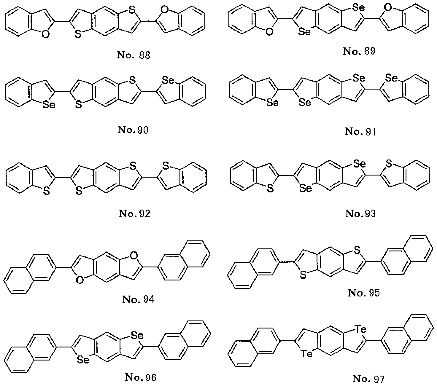
[0020] 又、式(1)で示される化合物のうち式 (4)で示されるフエ-ル置換された化合物以 外の具体例(化合物 No. 82〜化合物 No. I l l)を以下に示す。
[0021] [化 3]

No.82

No.84 No.85

[0022] [化 4]

No. 1 10 No. 1 1 1 次に、式(2)で示される化合物の具体例を示す。先ず、表 2には、式(2)で示される 化合物のうち、下記式(5)で表されるフエニル置換された化合物の例 (化合物 No. 1 12〜化合物 No. 137)を示す。表 2においては、フエ-ル基を Ph、 4 フエ-ルフエ 二ル基を 4 PhPh、ナフチル基を Np、チェ二ル基を Thとそれぞれ略記する。又、特
記されて!/、な!/、アルキル基は全て直鎖状のアルキル基である。
[化 5]

[0025] [表 2」 化
¾HHHHHHHHHHHHHHHHHHHHHHHHHF

[0026] 又、式(2)で示される化合物のうち式(5)で示されるフ -ル置換されたィ匕合物以 外の具体例(化合物 No. 138〜化合物 No. 151)を以下に示す。
[0027] [化 6]


No. 150 No. 151 次に、式(3)で示される化合物の具体例を示す。先ず、表 3には、式(3)で示される 化合物のうち、下記式 (6)で表されるフエニル置換されたィヒ合物の例 (ィヒ合物 No. 1 52〜化合物 No. 228)を示す。表 3においては、フエ二ル基を Ph、 4一フエ-ルフエ -ル基を 4一 PhPh、 4一ピリジル基を 4一 Py、ナフチル基を Np、チェ二ル基を Thと それぞれ略記する。又、特記されていないアルキル基は全て直鎖状のアルキル基で

8¾ ¾a n E¾ 。 9X sx
[ΐ- ε挲] [οεοο]

[6200]
Z60CS0/.00Zdf/X3d 91- l.9SZl/.00Z OAV
H H
^ H
H H H H H H H H H H si ZZ
H H ェ H H H H H H H H 3丄 s LZZ
H H
H H H H H H H H H H eS s 922
H Md H Hd H H Md H 4d H 3丄 3丄 933
H H dN H H H H dN H H 3丄 s丄 m,
^ H
H H H H H H H H &丄 3丄 ZZZ
H H HI H H H HI H H H H H 3丄 3丄 ZZZ
H H Hd H H H H Hd H H 3丄 3丄 \ZZ
H H HEOS H H H H H H H H H HEOS H H a丄 3丄 OZZ
H H W。)N H H H H 5(SH¾)N H H 3丄 3丄 &\.z
H H 6H"0000 H H H ^ H H H H H Woooo H H 9丄 3丄 21Z
H H £HOHNO0 H H H H eHOHNOO H H 3丄 3丄 L IZ
H H HOOO H H H H HOOO H H 3丄 3丄 91Z
H H £HOO H H H H εΗΟΟ H H 3丄 3丄 1Z
H H H H H H oo H H 3丄 3丄 HZ
J d d J d d d d d J 3丄 3丄 Ζ ΪΖ
H H NO H H H H NO H H 3上 3丄 Z iZ
H H d H H H H d H H a丄 s丄 HZ
H H ja H H H H H H 3上 3丄 OIZ
H H 3上 3丄 soz
H H a丄 3丄 soz

H H 3丄 3丄 902
Hd H 3S 3S ΌΖ
H H H H H H H H aS as
H H AO H H H H AO H H
H H H H H H H H aS zaz
H H 4上 H H H H 4丄 H H 10Z
H H Hd H H H H Hd H H as 3S ooz
H H !ΗΝΟΟ H H H H 'HNOO H H eS SS 66 ί
H H H H H H '(SH )N H H 3S 86 L
H H CHOOOO H H H H SH 003 H H SS 3S
H H εΗΟΗΝΟΟ H H H H eHOHNO0 H H eS SS 961.
H H EHOOO H H H H EH000 H H as SS 96 L
H H HOOO H H H H HOOO H H aS SS P61
H H HO H H H H HO H H eS SS Z6i
H H EHOO H H H H εΗ00 H H SS Z61
H H H H H H H H 161 d d d d J J J J d SS 061
H H NO H H H H NO H H 68 L
H H d H H H H d H H es SS 881
H H 」g H H H H H H as 81
H H 10 H H H H 10 H H 3S SS 981
Z60CS0/ .00Zdf/X3d 91· l .9SZl/ .00Z OAV
[0031] 又、式(3)で示される化合物のうち式 (6)で示されるフ -ル置換されたィ匕合物以 外の具体例(化合物 No. 229〜ィ匕合物 No. 250)を以下に示す。
[0032] [化 8]

[0033] [化 9]

[0034] 次に電子輸送型半導体材料の説明をする。電子輸送型の半導体材料としては、有 機'無機の材料が挙げられる。有機の半導体材料としては、ナフタレンテトラカルボン 酸無水物やそのイミド化物、ペリレンテトラカルボン酸無水物やそのイミド化物、ペン タセンのフッ素化物、フタロシアニンのフッ素化物、オリゴチォフェンのフッ化アルキ ル誘導体、(C60や C70などの)フラーレン類及びカーボンナノチューブ、カーボン ナノホーンなどのかご状炭素ナノ物質、無機の半導体材料としては、例えば n—ドー プされたシリコン、ゲルマニウムなど、また TiO 、 ZnO、 SnO 、 Nb O 、 WO 、 In O
2 2 2 5 3 2 3
、 SrTiO 、 Ta O 、 ZrO等の酸化物半導体、 GaAs、 InP、 CdS、 CdTe、 Cu S、 C
3 2 5 2 2 ulnSe 、 CuInSなどの化合物系が挙げられる。
2 2
好ましくは、有機系半導体であり、更に好ましくはフラーレン類及びカーボンナノチ ユーブ、カーボンナノホーンなどのかご状炭素ナノ物質が挙げられる。特に好ましくは
C60や C70などのフラーレンが挙げられる。
[0035] 本発明の電界効果トランジスタ(Field effect transistor;以下 FETと略することがある
)は、半導体に接して 2つの電極(ソース電極及びドレイン電極)があり、その電極間 に流れる電流を、ゲート電極と呼ばれるもう一つの電極に印加する電圧で制御するも のである。
[0036] 電界効果トランジスタとしては、ゲート電極が絶縁膜で絶縁されて 、る構造 (Metal
Insulator— Semiconductor; MIS構造)が一般的に用いられる。絶縁膜に金属 酸ィ匕膜を用いるものは MOS構造と呼ばれる。他には、ショットキー障壁を介してゲー ト電極が形成されて!ヽる構造 (MES)のものもあるが、有機半導体材料を用いた FET の場合、 MIS構造がよく用いられる。
[0037] 以下、図を用いて本発明の電界効果トランジスタについてより詳細に説明するが、 本発明はこれら構造には限られない。
図 1に、本発明の電界効果トランジスタ (素子)のいくつかの態様例を示す。各例に おいて、 1がソース電極、 2が半導体層、 3がドレイン電極、 4が絶縁体層、 5がゲート 電極、 6が基板をそれぞれ表す。尚、各層や電極の配置は、素子の用途により適宜 選択できる。 A〜Dは基板と並行方向に電流が流れるので、横型 FETと呼ばれる。 A はボトムコンタクト型構造、 Bはトップコンタクト型構造と呼ばれる。また、 Cは有機単結 晶の FET作成によく用いられる構造で、半導体上にソース及びドレイン電極、絶縁体 層を設け、さらにその上にゲート電極を形成している。 Dはトップ &ボトムコンタクト型 トランジスタと呼ばれる構造である。 Eは縦型の構造をもつ FETである静電誘導トラン ジスタ(SIT)の模式図である。この SIT構造によれば、電流の流れが平面状に広がる ので一度に大量のキャリアが移動できる。またソース電極とドレイン電極が縦に配され ているので電極間距離を小さくできるため応答が高速である。従って、大電流を流す 、あるいは高速のスイッチングを行うなどの用途に好ましく適用できる。
[0038] 各態様例における構成要素にっき説明する。
基板 6は、その上に形成される各層が剥離することなく保持できることが必要である 。例えば榭脂フィルム、紙、ガラス、石英、セラミックなどの絶縁性材料、金属や合金 などの導電性基板上にコーティング等により絶縁層を形成した物、榭脂と無機材料な ど各種組合せからなる材料等が使用しうる。使用しうる榭脂フィルムの例としては、例 えばポリエチレンテレフタレート、ポリエチレンナフタレート、ポリエーテルスルホン、ポ
リアミド、ポリイミド、ポリカーボネート、セノレローストリアセテート、ポリエーテルイミドな どが挙げられる。榭脂フィルムや紙を用いると、素子に可撓性を持たせることができ、 フレキシブルで、軽量となり、実用性が向上する。基板の厚さとしては、通常 1 μ m〜 10mmであり、好ましくは 5 μ m〜5mmである。
[0039] ソース電極 1、ドレイン電極 3、ゲート電極 5には導電性を有する材料が用いられる。
例えば、白金、金、銀、アルミニウム、クロム、タングステン、タンタル、ニッケル、コバ ルト、銅、鉄、鉛、錫、チタン、インジウム、パラジウム、モリブデン、マグネシウム、カル シゥム、バリウム、リチウム、カリウム、ナトリウム等の金属及びそれらを含む合金; InO
2
、 ZnO、 SnO、 ITO等の導電性酸化物;ポリア-リン、ポリピロール、ポリチォフェン
2 2
、ポリアセチレン、ポリパラフエ-レンビ-レン、ポリジアセチレン等の導電性高分子化 合物;シリコン、ゲルマニウム、ガリウム砒素等の半導体;カーボンブラック、フラーレン 、カーボンナノチューブ、グラフアイト等の炭素材料等が使用されうる。また、導電性 高分子化合物や半導体にはドーピングが行われて 、てもよ 、。その際のドーパントと しては、例えば、塩酸、硫酸、スルホン酸等の酸、 PF、 AsF、 FeCl等のルイス酸、
5 5 3
ヨウ素等のハロゲン原子、リチウム、ナトリウム、カリウム等の金属原子等が用いられる 。また、上記材料にカーボンブラックや金属粒子などを分散した導電性の複合材料も 用いられる。これらの材料は電極の仕事関数を変化させることが出来、電子及び正 孔の移動度を調整し、良好なアンノ《イポーラー特性を有する電界効果トランジスタを 得ることが出来る。
各電極 1、 3、 5には配線が連結されている力 配線も電極とほぼ同様の材料により 作製される。
[0040] 絶縁体層 4としては絶縁性を有する材料が用いられる。例えば、ポリパラキシリレン 、ポリアタリレート、ポリメチルメタタリレート、ポリスチレン、ポリビュルフエノール、ポリア ミド、ポリイミド、ポリカーボネート、ポリエステル、ポリビュルアルコール、ポリ酢酸ビ- ル、ポリウレタン、ポリスルホン、エポキシ榭脂、フエノール榭脂等のポリマー及びこれ らを組み合わせた共重合体;二酸化珪素、酸ィ匕アルミニウム、酸化チタン、酸化タン タル等の酸化物; SrTiO、 BaTiO等の強誘電性酸ィ匕物;窒化珪素、窒化アルミ-ゥ
3 3
ム等の窒化物;硫ィ匕物;フッ化物などの誘電体、あるいは、これら誘電体の粒子を分
散させたポリマー等が使用しうる。絶縁体層 4の膜厚は、材料によって異なるが、通常 0. lnm〜: LOO μ m、好ましくは 0. 5nm〜50 μ m、より好ましくは 5nm〜: L0 μ mであ る。
[0041] 半導体層 2の材料として、前記式(1)、(2)又は(3)で表される化合物の少なくとも 1 種と前述の電子輸送型の半導体材料が構成成分として用いられる。半導体層 2の材 料としては式(1)及び(3)の化合物が特に好ま 、。半導体層の材料はこれらの構 成成分の混合物を含んでいてもよいが、当該材料の総重量に対して、それぞれ式(1 )、 (2)または(3)で表される化合物と前述の電子輸送型の半導体材料を合計で 50 質量%以上、好ましくは 80質量%以上、更に好ましくは 95質量%以上含むことが必 要である。電界効果トランジスタの特性を改善したり他の特性を付与するために、必 要に応じて他の半導体材料や各種添加剤が混合や積層されて!ヽてもよ!ヽ。また半導 体層 2の構造としては、前記式(1)、(2)又は(3)で表される化合物と前述の電子輸 送型の半導体材料が混合された状態で単層構造をとつてもょ ヽし、積層構造をとつ てもよい。
半導体層 2の膜厚は、必要な機能を失わない範囲で、薄いほど好ましい。 A、 B及 び Dに示すような横型の電界効果トランジスタにおいては、所定以上の膜厚があれば 素子の特性は膜厚に依存しない一方、膜厚が厚くなると漏れ電流が増カロしてくること もあるためである。必要な機能を示すために、通常、 Inn!〜 10 /ζ πι、好ましくは 5nm 〜5 /ζ πι、より好ましくは 10ηπι〜3 /ζ πιである。前記式(1)、(2)又は(3)で表される 化合物と前述の電子輸送型の半導体材料が積層構造をとっている場合、トータルの 膜厚は前述と同じでょ ヽ。それぞれの膜厚は必要な機能を失わな ヽ範囲で任意に 調整できる。またこれらの材料の混合比率や膜厚を調整することによって、電子及び 正孔の移動度が変化すると考えられ、良好なアンノイポーラー特性を有する電界効 果トランジスタが得られる。
[0042] 本発明の電界効果トランジスタには各層の間や素子の外面に必要に応じて他の層 を設けることができる。例えば、半導体層上に直接または他の層を介して、保護層を 形成すると、湿度や酸素などの外気の影響を小さくすることができ、また、素子の ON ZOFF比を上げることが出来るなど、電気的特性を安定ィ匕できる利点もある。
保護層の材料としては特に限定されないが、例えば、エポキシ榭脂、ポリメチルメタ タリレート等のアクリル榭脂、ポリウレタン、ポリイミド、ポリビュルアルコール、フッ素榭 脂、ポリオレフイン等の各種樹脂からなる膜や、酸化珪素、酸ィ匕アルミニウム、窒化珪 素等、無機酸化膜や窒化膜等の誘電体からなる膜が好ましく用いられる。特に、酸 素や水分の透過率や吸水率の小さな榭脂(ポリマー)が好ましい。近年、有機 ELディ スプレイ用に開発されている保護材料も使用が可能である。保護層の膜厚は、その 目的に応じて任意の膜厚を採用できる力 通常 lOOnm〜: Lmmである。
[0043] また半導体が積層される基板または絶縁体層上などに表面処理を行うことにより、 素子の特性を向上させることが可能である。例えば基板表面の親水性 Z疎水性の度 合いを調整することにより、その上に成膜される膜の膜質を改良しうる。特に、有機半 導体材料は分子の配向など膜の状態によって特性が大きく変わることがある。そのた め、基板表面処理によって、基板とその後に成膜される半導体膜との界面部分の分 子配向が制御され、キャリア移動度等の特性が改良されるものと考えられる。このよう な基板処理としては、例えば、へキサメチルジシラザン、シクロへキセン、ォクタデシ ルトリクロロシラン等による疎水化処理、塩酸や硫酸、酢酸等による酸処理、水酸ィ匕 ナトリウム、水酸ィ匕カリウム、水酸ィ匕カルシウム、アンモニア等によるアルカリ処理、ォ ゾン処理、フッ素化処理、酸素やアルゴン等のプラズマ処理、ラングミュア 'ブロジェッ ト膜の形成処理、その他の絶縁体や半導体の薄膜の形成処理、機械的処理、コロナ 放電などの電気的処理、繊維等を利用したラビング処理等が挙げられる。
[0044] これらの態様にぉ 、て各層を設ける方法としては、例えば真空蒸着法、スパッタ法 、塗布法、印刷法、ゾルゲル法等が適宜採用できる。
[0045] 次に、本発明に係る電界効果トランジスタの製造方法について、図 1の態様例 Aに 示すボトムコンタクト型電界効果トランジスタ (FET)を例として、図 2に基づき以下に 説明する。
この製造方法は前記した他の態様の電界効果トランジスタ等にも同様に適用しうる ものである。
[0046] (基板及び基板処理)
基板 6上に必要な層や電極を設けることで作製される(図 2 (1)参照)。基板としては
上記で説明したものを用いうる。この基板上に前述の表面処理などを行うことも可能 である。基板 6の厚みは、必要な機能を妨げない範囲で薄い方が好ましい。材料によ つても異なるが、通常 1 μ m〜10mmであり、好ましくは 5 μ m〜5mmである。又、必 要により、基板に電極の機能を持たせるようにしてもょ ヽ。
[0047] (ゲート電極の形成)
基板 6上にゲート電極 5を形成する(図 2 (2)参照)。電極材料としては上記で説明 したものが用いられる。電極膜を成膜する方法としては、各種の方法を用いることが 出来、例えば真空蒸着法、スパッタ法、塗布法、熱転写法、印刷法、ゾルゲル法等が 採用される。成膜時又は成膜後、所望の形状になるよう必要に応じてパターユングを 行うのが好ましい。パターユングの方法としても各種の方法を用いうるが、例えばフォ トレジストのパター-ングとエッチングを組み合わせたフォトリソグラフィ一法等が挙げ られる。又、インクジェット印刷、スクリーン印刷、オフセット印刷、凸版印刷等の印刷 法、マイクロコンタクトプリンティング法等のソフトリソグラフィ一の手法、及びこれら手 法を複数組み合わせた手法を利用し、パターユングすることも可能である。ゲート電 極 5の膜厚は、材料によっても異なる力 通常 0. 1ηπι〜10 /ζ πιであり、好ましくは 0. 5nm〜5 μ mであり、より好ましくは lnm〜3 μ mである。又、ゲート電極と基板を兼 ねる場合は上記の膜厚より大きくてもよい。
[0048] (絶縁体層の形成)
ゲート電極 5上に絶縁層 4を形成する(図 2 (3)参照)。絶縁体材料としては上記で 説明したもの等が用られる。絶縁体層 4を形成するにあたっては各種の方法を用いう る。例えばスピンコーティング、スプレーコーティング、ディップコーティング、キャスト、 バーコート、ブレードコーティングなどの塗布法、スクリーン印刷、オフセット印刷、ィ ンクジヱット等の印刷法、真空蒸着法、分子線ェピタキシャル成長法、イオンクラスタ 一ビーム法、イオンプレーティング法、スパッタリング法、大気圧プラズマ法、 CVD法 などのドライプロセス法が挙げられる。その他、ゾルゲル法ゃアルミニウム上のアルマ イト、シリコンの熱酸化膜のように金属上に酸化物膜を形成する方法等が採用される 尚、絶縁体層と半導体層が接する部分においては、両層の界面で半導体分子を良
好に配向させるために、絶縁体層に所定の表面処理を行うことができる。表面処理の 手法は、基板の表面処理と同様のものが用いうる。絶縁体層 4の膜厚は、その機能を 損なわない範囲で薄い方が好ましい。通常 0. 1ηπι〜100 /ζ πιであり、好ましくは 0. 5nm〜50 μ mであり、より好ましくは 5nm〜: LO μ mである。
[0049] (ソース電極及びドレイン電極の形成)
ソース電極 1及びドレイン電極 3の形成方法等はゲート電極 5の場合に準じて形成 することが出来る(図 2 (4)参照)。
[0050] (半導体層の形成)
半導体材料としては上記で説明したような材料が使用される。半導体層を成膜する にあたっては、各種の方法を用いることが出来る。スパッタリング法、 CVD法、分子線 ェピタキシャル成長法、真空蒸着法等の真空プロセスでの形成方法と、ディップコー ト法、ダイコーター法、ロールコーター法、バーコ一ター法、スピンコート法等の塗布 法、インクジェット法、スクリーン印刷法、オフセット印刷法、マイクロコンタクト印刷法 などの溶液プロセスでの形成方法に大別される。以下、半導体層の形成方法につい て詳細に説明する。
[0051] まず、材料を真空プロセスによって成膜し半導体層を得る方法について説明する。
前記半導体材料をルツボゃ金属のボート中で真空下、加熱し、蒸発した半導体材 料を基板 (絶縁体層、ソース電極及びドレイン電極の露出部)に付着 (蒸着)させる方 法 (真空蒸着法)が好ましく採用される。この際、真空度は、通常 1. 0 X 10_1Pa以下 、好ましくは 1. O X 10_4Pa以下である。また、蒸着時の基板温度によって半導体膜、 ひ!ヽては電界効果トランジスタの特性が変化するので、注意深く基板温度を選択す るのが好ましい。蒸着時の基板温度は通常、 0〜200°C、好ましくは 10〜150°Cであ る。また、蒸着速度は、通常 0. OOlnmZ秒〜 lOnmZ秒であり、好ましくは 0. Oln mZ秒〜 InmZ秒である。半導体材料から形成される半導体層の膜厚は、通常 In m〜10 μ m、奸 しくは 5nm〜l μ mである。
尚、半導体層形成のための材料を加熱、蒸発させ基板に付着させる方法に代えて 、加速したアルゴン等のイオンを材料ターゲットに衝突させて材料原子を叩きだし基 板に付着させるスパッタリング法を用いてもよい。特に無機系の半導体材料は沸点が
高ぐ蒸着が困難なこともあり、様々なプロセスが使用できる。
また半導体材料を積層構造とするためには、順次に各々の材料を加熱、蒸発させ
、積層させることにより得られる。混合する場合には、通常、各々の材料を同時に加 熱、蒸発させる共蒸着により材料の混合した構造の半導体層を得ることが出来る。
[0052] 本発明における有機の半導体材料は、比較的低分子化合物であるため、このよう な真空プロセスが好ましく用いうる。このような真空プロセスには、やや高価な設備が 必要であるというものの、成膜性が良く均一な膜が得られやすいという利点がある。
[0053] 次に、半導体材料を溶液プロセスによって成膜し半導体層を得る方法について説 明する。この方法は一般的には溶媒に溶解する有機の半導体材料の場合に使用す ることが多ぐ無機系の材料の場合は均一な膜を作成することが通常、比較的困難で ある。
この方法では、前記材料を溶媒に溶解又は分散し、基板 (絶縁体層、ソース電極及 びドレイン電極の露出部)に塗布する。塗布の方法としては、キャスティング、スピンコ 一ティング、ディップコーティング、ブレードコーティング、ワイヤバーコーティング、ス プレーコーティング等のコーティング法や、インクジェット印刷、スクリーン印刷、オフ セット印刷、凸版印刷等の印刷法、マイクロコンタクトプリンティング法等のソフトリソグ ラフィ一の手法等、さらにはこれらの手法を複数組み合わせた方法を採用しうる。更 に、塗布方法に類似した方法として水面上に形成した単分子膜を基板に移し積層す るラングミュアプロジェクト法、液晶ゃ融液状態を 2枚の基板で挟んだり毛管現象で基 板間に導入する方法等も採用出来る。これらの方法により形成される半導体層の膜 厚は、機能を損なわない範囲で薄い方が好ましい。膜厚が大きくなると漏れ電流が 大きくなる懸念がある。半導体層の膜厚は、通常 1ηπι〜10 /ζ πι、好ましくは 5nm〜5 μ m、より好ましくは 10nm〜3 μ mである。
また半導体材料の混合膜は、各材料を一緒に溶解させ、上記のプロセスで成膜す ること〖こよって容易に得られる。しかし積層構造とするためには、それぞれの材料の 溶媒への溶解度の問題や、積層時に先に出来た膜が後から成膜する材料の溶液に 浸食されてしまうこともあり、成膜条件の最適化が必要となる。半導体層を形成するに あたり、このような溶液プロセスを用いると、比較的安価な設備で大面積の電界効果ト
ランジスタを製造できると 、う利点がある。
[0054] このように形成された半導体層(図 2 (5)参照)は、後処理によりさらに特性を改良す ることが可能である。例えば、加熱処理により、成膜時に生じた膜中の歪みを緩和す ることができ、特性の向上や安定ィ匕を図ることができる。さらに、酸素や水素等の酸化 性あるいは還元性の気体や液体にさらすこと〖こより、酸化ある!/、は還元による特性変 化を誘起することもできる。これは、例えば膜中のキャリア密度の増加あるいは減少の 目的で利用することができる。
[0055] また、ドーピングと呼ばれる手法おいて、微量の元素、原子団、分子、高分子を半 導体層に加えることにより、特性を変化させることができる。例えば、酸素、水素、塩 酸、硫酸、スルホン酸等の酸、 PF
5、 AsF
5、 FeCl等のルイス酸、ヨウ素等のハロゲン 3
原子、ナトリウム、カリウム等の金属原子等をドーピングすることが出来る。これは、半 導体層に対して、これらのガスを接触させたり、溶液に浸したり、電気化学的なドーピ ング処理をすることにより達成できる。これらのドーピングは膜の形成後でなくても、材 料合成時に添加したり、溶液からの作製プロセスでは、その溶液に添加したり、前駆 体膜の段階で添加することができる。また蒸着時に添加する材料を共蒸着したり、膜 形成時の雰囲気に混合したり、さらにはイオンを真空中で加速して膜に衝突させてド 一ビングすることも可能である。
[0056] これらのドーピングの効果は、キャリア密度の増加あるいは減少による電気伝導度 の変化、キャリアの極性の変化 (P型、 n型)、フェルミ準位の変化等が挙げられる。こ の様なドーピングは半導体素子では良く利用されているものである。
[0057] (保護層)
半導体層上に保護層 7を形成すると、外気の影響を最小限にでき、又、電界効果ト ランジスタの電気的特性を安定ィ匕できるという利点がある(図 2 (6)参照)。保護層材 料としては前記のものが使用される。保護層 7の膜厚は、その目的に応じて任意の膜 厚を採用できる力 通常 100nm〜lmmである。
保護層を成膜するにあたっては各種の方法を採用しうる。保護層が樹脂からなる場 合は、例えば、榭脂溶液を塗布後、乾燥させて榭脂膜とする方法、榭脂モノマーを塗 布あるいは蒸着したのち重合する方法などが挙げられる。成膜後に架橋処理を行つ
てもよい。保護層が無機物力もなる場合は、例えば、スパッタリング法、蒸着法等の真 空プロセスでの形成方法や、ゾルゲル法等の溶液プロセスでの形成方法も用いるこ とがでさる。
本発明の電界効果トランジスタにお 、ては半導体層上の他、各層の間にも必要に 応じて保護層を設けることが出来る。それらの層は電界効果トランジスタの電気的特 性の安定化に役立つ。
[0058] 本発明によれば、主に有機材料を半導体材料として用いて 、るため比較的低温プ ロセスでの製造が可能である。従って、高温にさらされる条件下では使用できなかつ たプラスチック板、プラスチックフィルム等フレキシブルな材質も基板として用いること ができる。その結果、軽量で柔軟性に優れた壊れにくい素子の製造が可能になり、 ディスプレイのアクティブマトリクスのスイッチング素子等として利用することができる。 ディスプレイとしては、例えば液晶ディスプレイ、高分子分散型液晶ディスプレイ、電 気泳動型ディスプレイ、 ELディスプレイ、エレクト口クロミック型ディスプレイ、粒子回 転型ディスプレイ等が挙げられる。また、本発明の電界効果トランジスタは塗布法ある いは印刷プロセスでの製造が可能であることから、大面積ディスプレイの製造にも適 している。
[0059] 本発明の電界効果トランジスタは、アンバイポーラ一型であるために、簡便に CMO S回路を形成することが可能になると期待される。通常は、 N型と P型の半導体材料を 別々にパータンユングすることで CMOS回路の作製は可能である力 製造プロセス が煩雑となり、コストも高いものになってしまう。しかし、本発明の電界効果トランジスタ により非常にコストを安くすることが可能となると考えられる。
また、本発明の電界効果トランジスタによって形成された CMOS回路は、メモリー 回路素子、信号ドライバー回路素子、信号処理回路素子などのデジタル素子やアナ ログ素子としても利用できる。さらにこれらを組み合わせることにより ICカードや ICタグ の作製が可能となる。更に、本発明の電界効果トランジスタは、化学物質等の外部刺 激によりその特性に変化を起こすことができるので、 FETセンサーとしての利用も可 能である。
[0060] 電界効果トランジスタの動作特性は、半導体層のキャリア移動度、電導度、絶縁層
の静電容量、素子の構成 (ソース'ドレイン電極間距離及び幅、絶縁層の膜厚等)な どにより決まる。電界効果トランジスタに用いる半導体用の材料としては、キャリア移 動度が高 、ものほど好ま U、。
これまでにも比較的高い移動度を真空中で示す素子の報告は幾つ力あつたが、大 気中で安定に高移動度のアンバイポーラ一特性を示す報告はされていな力つた。そ れに対して、本発明における式(1)、式(2)または式(3)で表される化合物を少なくと も 1種と電子輸送型の半導体材料を有することを特徴とする電界効果トランジスタは、 大気中で高い移動度を示し、アンバイポーラ一特性を有する。特に各々の材料を積 層構造とすることで、単層の状態と比較して高い移動度と、大気中における高い安定 性を示す。さらに、本発明の電界効果トランジスタは長期間にわたって劣化が少ない 安定なアンバイポーラ一特性を示す。また、本発明の電界効果トランジスタは、複雑 な製造プロセスを経ずに安価な半導体回路が作製でき、さらに長期間にわたって安 定な電気特性を有し、安定性が高く寿命が長い電子回路が得られるという利点があ る。
実施例
[0061] 以下、実施例を挙げて本発明を更に詳細に説明するが、本発明はこれらの例に限 定されるものではない。実施例中、部は特に指定しない限り質量部を、また%は質量 %をそれぞれ表す。
[0062] 合成例 1
J.Am.Chem.Soc, 1997,119,4578.に記載の方法に従って得られた 1, 4 ジブロモ - 2, 5 ビス(フエ-ルェチュル)ベンゼン 1部をテトラヒドロフラン 18部に溶解し、 - 78°Cで 1. 6モル t—ブチルリチウム(ペンタン溶液) 6部をカ卩えてリチオイ匕した後、セ レン粉末 0. 2部と反応させることにより黄色粉末を得た。得られた粉末を真空昇華精 製を行い、化合物(34)の精製物 0. 3gを得た。
合成例 2
合成例 1のセレン粉末の代わりに硫黄粉末を用いることで、化合物(1)の精製物 0. 3gを得た。
[0063] 合成例 3
非特許文献 S.Y.Zherdeva et al.Zh.Organi.Khimi, 1980, 16,430を参考に、 1から 4 の合成を以下のように行った。市販の化合物である 1をクロロスルホン酸中で加熱す ることで 2へと定量的に変換した。続いて 2を酢酸中に懸濁し、 55%ヨウ化水素酸を 加えて加熱し、生成した沈殿を一且濾取後、再度、沈殿物を酢酸中に臭素とともに 混合'加熱して 3を黄色の沈殿物として得た。さらに、 3と薄片状の錫を酢酸中に加え 加熱し、濃塩酸を徐々に加えることで 4を白色の沈殿として得た。
4 (2g)をエタノール(60mL)、硫酸 (4. OmL)と混合し、これに亜硝酸イソアミル(3 . OmL)をカ卩えた後、ヨウ化カリウム(3. 6g)と反応させることで、ジョード体 5 (2. 9g) を得た。続いて、 5 (0. 5g)とフエ-ルポロン酸 (0. 3g)、リン酸三カリウム(3. 4g)を D MF (20ml)中で、パラジウム'テトラキストリフエ-ルホスフィン(0. lg)存在下、反応 させることで DPh— BTBT(0. 2g)を得た。
[化 10]

s 実施例 1
へキサメチルジシラザン処理を行った 300nmの SiO熱酸化膜付き nドープシリコン
2
ウェハー(面抵抗 0. 02 Ω 'cm以下)上に、レジスト材料を塗布、露光パターユングし 、ここにクロムを lnm、さらに金を 40nm蒸着した。次いでレジストを剥離して、ソース 電極(1)及びドレイン電極 (3)を形成させた(チャネル長 25 m Xチャネル幅 4mm X 19個であるくし型電極)。この電極の設けられたシリコンウェハーを真空蒸着装置 内に設置し、装置内の真空度が 1. 0 X 10_3Pa以下になるまで排気した。抵抗加熱
蒸着法によって、化合物 No. 34 (式 (4)及び表 1参照)を 30nmの厚さに、次いで C6 0フラーレンを 30nmの厚さに室温(25°C)にて蒸着し、半導体層(2)を形成して本発 明の電界効果トランジスタを得た。本実施例の有機系電界効果トランジスタにぉ 、て は、熱酸ィ匕膜付き nドープシリコンゥヱハーにおける熱酸ィ匕膜が絶縁層(4)の機能を 有し、 nドープシリコンウェハーが基板 (6)及びゲート層(5)の機能を有して 、る(図 3 を参照)。
[0065] 得られた電界効果トランジスタを真空プロ一バー内に設置し、真空ポンプで約 5 X 1 0_ 3Paに減圧し、半導体パラメーターアナライザー 4155C (Agilent社製)を用 、て 半導体特性を測定した。半導体特性はゲート電圧を 10Vから 100Vまで 10Vステ ップで走査し、又ドレイン電圧を 10Vから 100Vまで走査し、ドレイン電流 ドレイ ン電圧を測定した。その結果、電流飽和が観測され、その飽和領域力 求めた正孔 移動度は 0. 10cm2ZVsであった。逆にゲート電圧を— 10Vから 100Vまで 10Vステ ップで走査し、又ドレイン電圧を 10Vから 100Vまで走査し、ドレイン電流 ドレイ ン電圧を測定した。その結果、電流飽和が観測され、その飽和領域力 求めた電子 移動度は 0. 10cm2ZVsであり、アンノイポーラー特性の発現が観測された。また、 同じ素子を大気中で測定した場合の正孔移動度は 1. 6 X 10_2cm2ZV' Sで電子移 動度は 5. 9 X 10_4cm2ZV' sのアンバイポーラ一特性を示した。
[0066] 実施例 2
実施例 1において、化合物 No. 34をィ匕合物 No. 1 (式 (4)及び表 1参照)に変更し た以外は実施例 1と同様にして、本発明の電界効果トランジスタを作製した。半導体 特性を測定した結果、電流飽和が観測された。得られた電圧電流曲線より、本素子 はアンノイポーラー型の特性を示し、その正孔移動度は 0. 10cmVv- s,電子移動 度は 0. 17cm2ZV' sであった。また、同じ素子を大気中で測定した場合の正孔移動 度は 1. 2 X 10_2cm2/V' sで電子移動度は 1. 2 X 10_3cm2/V' sのアンバイポー ラー特性を示した。
[0067] 実施例 3
実施例 1において、半導体層(2)として化合物 No. 34 (式 (4)及び表 1参照)を 30η mの厚さに、次いで C60フラーレンと CuPc (l : l)の共蒸着層を 10nmの厚さに、さら
に C60を 20nmの厚さにさらに 2, 9—ジメチノレー 4, 7—ジフエ-ノレ一 1, 10—フエナ ントロリンを lOnmの厚さに室温(25°C)にて蒸着した以外は実施例 1と同様にして、 本発明の電界効果トランジスタを作製した。大気下にて半導体特性を測定した結果、 電流飽和が観測された。得られた電圧電流曲線より、本素子はアンバイポーラ一型 の特性を示し、その正孔移動度は 1. 2 X 10_1cm2ZV' s、電子移動度は 7. 0 X 10 cm ZV' sであつ 7こ。
[0068] 実施例 4
実施例 1において、半導体層(2)として化合物 No. 1 (式 (4)及び表 1参照)を 10η mの厚さに、次いで C60を lOnmの厚さに、さらに化合物 No. 1を 60nmの厚さに室 温 (25°C)にて蒸着した以外は実施例 1と同様にして、本発明の電界効果トランジス タを作製した。半導体特性を測定した結果、電流飽和が観測され、得られた電圧電 流曲線より、本素子はアンバイポーラ一型の特性を示し、その正孔移動度は 5. 8 X 1 0"2cmVv-s,電子移動度は 0. 25cm2ZV' sであった。
[0069] 実施例 5
実施例 1において、化合物 No. 34をィ匕合物 No. 152 (式 (6)及び表 3参照)に変 更した以外は実施例 1と同様にして、本発明の電界効果トランジスタを作製した。半 導体特性を測定した結果、電流飽和が観測され、得られた電圧電流曲線より、本素 子はアンノイポーラー型の特性を示し、その正孔移動度は 8. 5 X 10"4cmVv-s, 電子移動度は 6. 6 X 10_2cm2ZV' Sであった。また同じ素子を大気中で測定した場 合の正孔移動度は 2. 5 X 10_4cm2/V' sで電子移動度は 6. 1 X 10"4cmVv-s のアンノイポーラー特性を示した。
[0070] 実施例 6
実施例 1において、半導体層(2)として化合物 No. 34 (式 (4)及び表 1参照)を 30 nmの厚さに、次いで C60を 30nmの厚さに、さらに 2, 9—ジメチノレー 4, 7—ジフエ- ルー 1, 10—フエナント口リンを 30nmの厚さに室温(25°C)にて蒸着した以外は実施 例 1と同様にして、本発明の電界効果トランジスタを作製した。半導体特性を測定し た結果、電流飽和が観測され、得られた電圧電流曲線より、本素子はアンバイポーラ 一型の特性を示し、その正孔移動度は 9. 4 X 10"2cmVv-s,電子移動度は 0. 14
cm2ZV' sであった。また同じ素子を大気中で測定した場合の正孔移動度は 2. O X 10_2cm2/V' sで電子移動度は 2. O X 10_2cm2/V' sのアンバイポーラ一特性を 示した。
[0071] 実施例 7
300nmの SiO熱酸化膜付き nドープシリコンウェハー(面抵抗 0. 02 Ω 'cm以下)
2
を真空蒸着装置内に設置し、装置内の真空度が 1. 0 X 10_3Pa以下になるまで排気 した。抵抗加熱蒸着法によって、化合物 No. 34 (式 (4)及び表 1参照)を 15nmの厚 さに、次いで C60フラーレンを 40nmの厚さに室温 (25°C)にて蒸着し、半導体層(2) を形成した。引き続き電極作製の為、マスクを設置した後、抵抗加熱蒸着法によって 、金の電極(ソース及びドレイン電極:チャネル長 100 m Xチャネル幅 2mm)を 40 nmの厚さに蒸着し、本発明の電界効果トランジスタを得た。本実施例における電界 効果トランジスタはトップコンタクト型であり、熱酸ィ匕膜付き nドープシリコンウェハーに おける熱酸化膜が絶縁体層(4)の機能を有し、 nドープシリコンウェハーが基板 (6) 及びゲート電極 (5)の機能を有して 、る(図 1 Bを参照)。
得られた電界効果トランジスタを真空プロ一バー内に設置し、真空ポンプで約 5 X 1 0_ 3Paに減圧し、半導体パラメーターアナライザー 4155C (Agilent社製)を用 、て 半導体特性を測定した。半導体特性はゲート電圧を 10Vから 60Vまで 10Vステツ プで走査し、又ドレイン電圧を 10Vから 60Vまで走査し、ドレイン電流 ドレイン電 圧を測定した。その結果、電流飽和が観測され、その飽和領域から求めた正孔移動 度は 0. 13cm2ZVs、閾値電圧は— 33 Vであった。逆にゲート電圧を— 10Vから 60 Vまで 10Vステップで走査し、又ドレイン電圧を— 10Vから 60Vまで走査し、ドレイン 電流 ドレイン電圧を測定した。その結果、電流飽和が観測され、その飽和領域から 求めた電子移動度は 2. 95cm Vs,閾値電圧は 37Vであり、アンバイポーラー特 性の発現が観測された。
[0072] 実施例 8
実施例 7において、化合物 No. 34の膜厚を 60nmに変更した以外は実施例 7と同 様にして、本発明の電界効果トランジスタを作製した。得られた電界効果トランジスタ を真空プロ一バー内に設置し、同様に半導体特性を測定した。その結果、電流飽和
が観測され、その飽和領域力 求めた正孔移動度は 0. 15cm Vs,電子移動度は 1. 03cm2ZVsでありアンバイポーラ一特性の発現が観測された。
[0073] 実施例 9
へキサメチルジシラザン処理を行った 300nmの SiO熱酸化膜付き nドープシリコン
2
ウェハー(面抵抗 0. 02 Ω 'cm以下)を真空蒸着装置内に設置し、装置内の真空度 が 1. 0 X 10_3Pa以下になるまで排気した。抵抗加熱蒸着法によって、化合物 No. 1 52 (式(6)及び表 3参照)を 40nmの厚さに、次!、で C60フラーレンを 40nmの厚さに 室温 (25°C)にて蒸着し、半導体層(2)を形成した。引き続き電極作製の為、マスクを 設置した後、抵抗加熱蒸着法によって、金の電極 (ソース及びドレイン電極:チャネル 長 50 mXチャネル幅 2mm)を 40nmの厚さに蒸着し、本発明の電界効果トランジ スタを得た。本実施例における電界効果トランジスタはトップコンタクト型であり、熱酸 化膜付き nドープシリコンウェハーにおける熱酸ィ匕膜が絶縁体層(4)の機能を有し、 n ドープシリコンウェハーが基板 (6)及びゲート電極 (5)の機能を有して 、る(図 1—B を参照)。
得られた電界効果トランジスタを真空プロ一バー内に設置し、大気下における半導 体特性を測定した。半導体特性はゲート電圧を 10Vから— 100Vまで 20Vステップ で走査し、又ドレイン電圧を 10Vから 100Vまで走査し、ドレイン電流 ドレイン電 圧を測定した。その結果、電流飽和が観測され、その飽和領域から求めた正孔移動 度は 0. 23cm Vs,閾値電圧は— 45Vであった。逆にゲート電圧を— 10Vから 10 0Vまで 20Vステップで走査し、又ドレイン電圧を— 10Vから 100Vまで走査し、ドレイ ン電流 ドレイン電圧を測定した。その結果、電流飽和が観測され、その飽和領域か ら求めた電子移動度は 0. 21cm2ZVs、閾値電圧は 34Vであり、アンバイポーラ一 特性の発現が観測された。
産業上の利用可能性
[0074] 本発明による特定の有機複素環化合物と電子輸送型の半導体材料を有する電界 効果トランジスタは、実用的な水準の電荷移動度を有し、大気中での安定性に優れ たアンバイポーラ一型電界効果トランジスタとして広く使用されうる。
図面の簡単な説明
[0075] [図 1]本発明の電界効果トランジスタの構造態様例を示す概略図である。
[図 2]本発明の電界効果トランジスタの一態様例を製造する為の工程の概略図である
[図 3]実施例 1で得られた本発明の電界効果トランジスタの概略図である。
符号の説明
[0076] 1ソース電極
2半導体層
3ドレイン電極
4絶縁体層
5ゲート電極
6基板
7保護層
Claims
[化 1]

(式中、 X〜Xはそれぞれ独立に硫黄原子、セレン原子又はテルル原子を、 R〜R
1 6 1 6 はそれぞれ独立に置換されて 、てもよ 、芳香族基を表す。 )
[2] 電子輸送型の半導体材料がフラーレン、カーボンナノチューブ及びカーボンナノホ ーンカもなる群力も選ばれるかご状炭素ナノ物質である、請求項 1に記載の電界効 果トランジスタ。
[3] 電子輸送型の半導体材料がフラーレンである、請求項 2に記載の電界効果トランジ スタ。
[4] 式(1)、(2)または(3)で表される化合物の少なくとも 1種を含む層と、電子輸送型 の半導体材料を含む層が積層構造を有している、請求項 1〜3のいずれか 1項に記 載の電界効果トランジスタ。
[5] 絶縁体層と、それにより隔離されたゲート電極及びその絶縁体層に接するように設 けられたソース電極とドレイン電極を有するボトムコンタクト型構造の電極上に、式(1 )、 (2)または(3)で表される化合物を含む層、及び電子輸送型の半導体材料を含む 層が積層されている、請求項 1〜4のいずれか 1項に記載の電界効果トランジスタ。
[6] ゲート電極上に設けられた絶縁体層上に、式(1)、 (2)または(3)で表される化合 物を含む層、及び電子輸送型の半導体材料を含む層が積層され、さらに該層の最 上部に接するようにソース電極及びドレイン電極がそれぞれ設けられているトップコン
タクト型の、請求項 1〜4のいずれ力 1項に記載の電界効果トランジスタ。 大気下で電子と正孔の電荷にぉ 、て 0. 01cm2ZVs以上の移動度を示す、 項 1〜6のいずれ力 1項に記載のアンバイポーラ一型電界効果トランジスタ。
Priority Applications (1)
| Application Number | Priority Date | Filing Date | Title |
|---|---|---|---|
| JP2008513095A JP5167560B2 (ja) | 2006-03-31 | 2007-02-20 | 電界効果トランジスタ |
Applications Claiming Priority (2)
| Application Number | Priority Date | Filing Date | Title |
|---|---|---|---|
| JP2006099683 | 2006-03-31 | ||
| JP2006-099683 | 2006-03-31 |
Publications (1)
| Publication Number | Publication Date |
|---|---|
| WO2007125671A1 true WO2007125671A1 (ja) | 2007-11-08 |
Family
ID=38655211
Family Applications (1)
| Application Number | Title | Priority Date | Filing Date |
|---|---|---|---|
| PCT/JP2007/053092 Ceased WO2007125671A1 (ja) | 2006-03-31 | 2007-02-20 | 電界効果トランジスタ |
Country Status (3)
| Country | Link |
|---|---|
| JP (1) | JP5167560B2 (ja) |
| TW (1) | TW200802864A (ja) |
| WO (1) | WO2007125671A1 (ja) |
Cited By (17)
| Publication number | Priority date | Publication date | Assignee | Title |
|---|---|---|---|---|
| JPH0364737A (ja) * | 1989-08-02 | 1991-03-20 | Sharp Corp | 液晶表示装置 |
| JP2009246140A (ja) * | 2008-03-31 | 2009-10-22 | Hiroshima Univ | 発光素子 |
| JP2009267132A (ja) * | 2008-04-25 | 2009-11-12 | Mitsui Chemicals Inc | 有機トランジスタ |
| JP2010010549A (ja) * | 2008-06-30 | 2010-01-14 | Konica Minolta Holdings Inc | 薄膜トランジスタの製造方法及び薄膜トランジスタ |
| JP2010016037A (ja) * | 2008-07-01 | 2010-01-21 | Konica Minolta Holdings Inc | 薄膜トランジスタの製造方法 |
| WO2010058833A1 (ja) * | 2008-11-21 | 2010-05-27 | 国立大学法人広島大学 | 新規な複素環式化合物及びその利用 |
| WO2012010292A1 (en) | 2010-07-21 | 2012-01-26 | Heraeus Clevios Gmbh | SEMICONDUCTORS BASED ON SUBSTITUTED [1]BENZOTHIENO[3,2-b] [1]-BENZOTHIOPHENES |
| JP5370771B2 (ja) * | 2007-05-24 | 2013-12-18 | 日本化薬株式会社 | 芳香族化合物の製造方法 |
| JP2014033194A (ja) * | 2012-07-13 | 2014-02-20 | Semiconductor Energy Lab Co Ltd | 半導体装置 |
| JP2015053497A (ja) * | 2011-03-10 | 2015-03-19 | 国立大学法人東京工業大学 | 有機半導体材料 |
| JP2016105502A (ja) * | 2008-07-16 | 2016-06-09 | シーブライト・インコーポレイテッドCbrite Inc. | 金属酸化物半導体装置および半導体装置を製造する方法 |
| JP2016136638A (ja) * | 2010-01-22 | 2016-07-28 | 株式会社半導体エネルギー研究所 | 半導体装置 |
| JP2016189476A (ja) * | 2010-05-20 | 2016-11-04 | 株式会社半導体エネルギー研究所 | 半導体装置の作製方法 |
| WO2017159684A1 (ja) * | 2016-03-15 | 2017-09-21 | ソニー株式会社 | 光電変換素子および固体撮像装置 |
| EP3617212A1 (en) * | 2018-08-28 | 2020-03-04 | Samsung Electronics Co., Ltd. | Compound and thin film transistor and electronic device |
| CN112992968A (zh) * | 2015-07-17 | 2021-06-18 | 索尼公司 | 光电转换元件、图像拾取元件、层叠型图像拾取元件和固态图像拾取装置 |
| KR20240027597A (ko) | 2021-06-30 | 2024-03-04 | 소니 세미컨덕터 솔루션즈 가부시키가이샤 | 반도체 소자 및 반도체 장치 |
Families Citing this family (4)
| Publication number | Priority date | Publication date | Assignee | Title |
|---|---|---|---|---|
| JP5487655B2 (ja) * | 2008-04-17 | 2014-05-07 | 株式会社リコー | [1]ベンゾチエノ[3,2‐b][1]ベンゾチオフェン化合物およびその製造方法、それを用いた有機電子デバイス |
| WO2009129912A1 (en) * | 2008-04-24 | 2009-10-29 | Merck Patent Gmbh | Electronic device |
| TWI394306B (zh) * | 2008-08-26 | 2013-04-21 | Univ Nat Chiao Tung | 光電記憶體元件、其製造以及量測方法 |
| US11066418B2 (en) | 2018-11-26 | 2021-07-20 | Samsung Electronics Co., Ltd. | Compound and thin film transistor and electronic device |
Citations (1)
| Publication number | Priority date | Publication date | Assignee | Title |
|---|---|---|---|---|
| JP2005154371A (ja) * | 2003-11-27 | 2005-06-16 | Japan Science & Technology Agency | 新規なベンゾジカルコゲノフェン誘導体、その製造方法およびそれを用いた有機半導体デバイス |
Family Cites Families (2)
| Publication number | Priority date | Publication date | Assignee | Title |
|---|---|---|---|---|
| US6278127B1 (en) * | 1994-12-09 | 2001-08-21 | Agere Systems Guardian Corp. | Article comprising an organic thin film transistor adapted for biasing to form a N-type or a P-type transistor |
| JP2007273594A (ja) * | 2006-03-30 | 2007-10-18 | Nippon Kayaku Co Ltd | 電界効果トランジスタ |
-
2007
- 2007-02-20 WO PCT/JP2007/053092 patent/WO2007125671A1/ja not_active Ceased
- 2007-02-20 JP JP2008513095A patent/JP5167560B2/ja not_active Expired - Fee Related
- 2007-02-27 TW TW096106876A patent/TW200802864A/zh unknown
Patent Citations (1)
| Publication number | Priority date | Publication date | Assignee | Title |
|---|---|---|---|---|
| JP2005154371A (ja) * | 2003-11-27 | 2005-06-16 | Japan Science & Technology Agency | 新規なベンゾジカルコゲノフェン誘導体、その製造方法およびそれを用いた有機半導体デバイス |
Non-Patent Citations (3)
| Title |
|---|
| CHIKADA Y. ET AL.: "Benzo Selenophene Kokkaku o Kiban toshiba Shinki Yuki FET Zairyo no Kaihatsu", CSJ: THE CHEMICAL SOCIETY OF JAPAN KOEN YOKOSHU, vol. 85TH, no. 1, 11 March 2005 (2005-03-11), pages 500 + ABSTR. NO. 3H7-41, XP003018917 * |
| EBATA H. ET AL.: "[1]Benzothieno[2,3-b]Benzothiophene Yudotai no Gosei to Sono FET Tokusei", CSJ: THE CHEMICAL SOCIETY OF JAPAN KOEN YOKOSHU, vol. 86TH, no. 1, 11 March 2006 (2006-03-11), pages 561, XP003018937 * |
| EBATA H. ET AL.: "Denshi Kyuinsei Chikanki o Donyu shita Benzo [1,2-b:4,5-b'] Dichalcogenophene Yudotai no FET Tokusei", CSJ: THE CHEMICAL SOCIETY OF JAPAN KOEN YOKOSHU, vol. 85TH, no. 1, 11 March 2005 (2005-03-11), pages 500 * |
Cited By (34)
| Publication number | Priority date | Publication date | Assignee | Title |
|---|---|---|---|---|
| JPH0364737A (ja) * | 1989-08-02 | 1991-03-20 | Sharp Corp | 液晶表示装置 |
| JP5370771B2 (ja) * | 2007-05-24 | 2013-12-18 | 日本化薬株式会社 | 芳香族化合物の製造方法 |
| JP2009246140A (ja) * | 2008-03-31 | 2009-10-22 | Hiroshima Univ | 発光素子 |
| JP2009267132A (ja) * | 2008-04-25 | 2009-11-12 | Mitsui Chemicals Inc | 有機トランジスタ |
| JP2010010549A (ja) * | 2008-06-30 | 2010-01-14 | Konica Minolta Holdings Inc | 薄膜トランジスタの製造方法及び薄膜トランジスタ |
| JP2010016037A (ja) * | 2008-07-01 | 2010-01-21 | Konica Minolta Holdings Inc | 薄膜トランジスタの製造方法 |
| JP2016105502A (ja) * | 2008-07-16 | 2016-06-09 | シーブライト・インコーポレイテッドCbrite Inc. | 金属酸化物半導体装置および半導体装置を製造する方法 |
| KR101556095B1 (ko) * | 2008-11-21 | 2015-09-30 | 니폰 가야꾸 가부시끼가이샤 | 신규의 헤테로고리 화합물 및 그 이용 |
| WO2010058833A1 (ja) * | 2008-11-21 | 2010-05-27 | 国立大学法人広島大学 | 新規な複素環式化合物及びその利用 |
| US8313671B2 (en) | 2008-11-21 | 2012-11-20 | Hiroshima University | Heterocyclic compound and use thereof |
| US9865744B2 (en) | 2010-01-22 | 2018-01-09 | Semiconductor Energy Laboratory Co., Ltd. | Semiconductor device |
| JP2016136638A (ja) * | 2010-01-22 | 2016-07-28 | 株式会社半導体エネルギー研究所 | 半導体装置 |
| JP2016189476A (ja) * | 2010-05-20 | 2016-11-04 | 株式会社半導体エネルギー研究所 | 半導体装置の作製方法 |
| US9780229B2 (en) | 2010-05-20 | 2017-10-03 | Semiconductor Energy Laboratory Co., Ltd. | Method for manufacturing semiconductor device |
| DE102010031897A1 (de) | 2010-07-21 | 2012-01-26 | Heraeus Clevios Gmbh | Halbleiter auf Basis substituierter [1] Benzothieno[3,2-b][1]-benzothiophene |
| WO2012010292A1 (en) | 2010-07-21 | 2012-01-26 | Heraeus Clevios Gmbh | SEMICONDUCTORS BASED ON SUBSTITUTED [1]BENZOTHIENO[3,2-b] [1]-BENZOTHIOPHENES |
| JP2015053497A (ja) * | 2011-03-10 | 2015-03-19 | 国立大学法人東京工業大学 | 有機半導体材料 |
| US10937964B2 (en) | 2011-03-10 | 2021-03-02 | Tokyo Institute Of Technology | Organic semiconductor material |
| US10056557B2 (en) | 2011-03-10 | 2018-08-21 | Tokyo Institute Of Technology | Organic semiconductor material |
| JP2014033194A (ja) * | 2012-07-13 | 2014-02-20 | Semiconductor Energy Lab Co Ltd | 半導体装置 |
| CN112992968A (zh) * | 2015-07-17 | 2021-06-18 | 索尼公司 | 光电转换元件、图像拾取元件、层叠型图像拾取元件和固态图像拾取装置 |
| WO2017159684A1 (ja) * | 2016-03-15 | 2017-09-21 | ソニー株式会社 | 光電変換素子および固体撮像装置 |
| JPWO2017159684A1 (ja) * | 2016-03-15 | 2019-03-14 | ソニー株式会社 | 光電変換素子および固体撮像装置 |
| WO2017159025A1 (ja) * | 2016-03-15 | 2017-09-21 | ソニー株式会社 | 光電変換素子および固体撮像装置 |
| US11398605B2 (en) | 2016-03-15 | 2022-07-26 | Sony Corporation | Photoelectric conversion element and solid-state imaging device |
| JP7107217B2 (ja) | 2016-03-15 | 2022-07-27 | ソニーグループ株式会社 | 光電変換素子および固体撮像装置 |
| JP2022130690A (ja) * | 2016-03-15 | 2022-09-06 | ソニーグループ株式会社 | 光電変換素子および固体撮像装置 |
| EP3617212A1 (en) * | 2018-08-28 | 2020-03-04 | Samsung Electronics Co., Ltd. | Compound and thin film transistor and electronic device |
| CN110862402A (zh) * | 2018-08-28 | 2020-03-06 | 三星电子株式会社 | 化合物、有机薄膜、薄膜晶体管和电子器件 |
| KR20200024609A (ko) * | 2018-08-28 | 2020-03-09 | 삼성전자주식회사 | 화합물, 박막 트랜지스터 및 전자 소자 |
| US11450810B2 (en) | 2018-08-28 | 2022-09-20 | Samsung Electronics Co., Ltd. | Compound and thin film transistor and electronic device |
| KR102631401B1 (ko) * | 2018-08-28 | 2024-01-29 | 삼성전자주식회사 | 화합물, 박막 트랜지스터 및 전자 소자 |
| CN110862402B (zh) * | 2018-08-28 | 2024-07-26 | 三星电子株式会社 | 化合物、有机薄膜、薄膜晶体管和电子器件 |
| KR20240027597A (ko) | 2021-06-30 | 2024-03-04 | 소니 세미컨덕터 솔루션즈 가부시키가이샤 | 반도체 소자 및 반도체 장치 |
Also Published As
| Publication number | Publication date |
|---|---|
| JPWO2007125671A1 (ja) | 2009-09-10 |
| JP5167560B2 (ja) | 2013-03-21 |
| TW200802864A (en) | 2008-01-01 |
Similar Documents
| Publication | Publication Date | Title |
|---|---|---|
| WO2007125671A1 (ja) | 電界効果トランジスタ | |
| JP5477978B2 (ja) | 電界効果トランジスタ | |
| JP5428104B2 (ja) | 有機半導体組成物 | |
| WO2008047896A1 (en) | Field-effect transistor | |
| JP5840197B2 (ja) | 有機電界効果トランジスタ及び有機半導体材料 | |
| KR102027362B1 (ko) | 반도체 조성물 | |
| JP2007266285A (ja) | 電界効果トランジスタ | |
| JP5160078B2 (ja) | 電界効果トランジスタ | |
| JP4529571B2 (ja) | 電界効果トランジスタ | |
| KR101462526B1 (ko) | 유기 반도체 재료 및 전계 효과 트랜지스터 그리고 그의 제조 방법 | |
| JP2012044109A (ja) | 電界効果トランジスタ及びその製造方法 | |
| JP2015199716A (ja) | 多環縮環化合物、有機半導体材料、有機半導体デバイス及び有機トランジスタ | |
| CN102194998B (zh) | 有机半导体元件和有机电极 | |
| JP2007273594A (ja) | 電界効果トランジスタ | |
| JP5428113B2 (ja) | 電界効果トランジスタ | |
| JP6592863B2 (ja) | 有機化合物及びその用途 | |
| JP2007266411A (ja) | 電界効果トランジスタ | |
| JP4506228B2 (ja) | 有機電界効果トランジスタ、表示素子及び電子ペーパー | |
| JP6917106B2 (ja) | 縮合多環芳香族化合物及びその用途 | |
| JP4868825B2 (ja) | 有機系電界効果トランジスタ | |
| KR101823523B1 (ko) | 그래핀 양자점 박막, 이의 제조 방법, 및 상기 그래핀 양자점 박막을 이용하는 박막 트랜지스터 | |
| JP6526585B2 (ja) | 縮合多環芳香族化合物及びその用途 | |
| JP2005033185A (ja) | 電界効果トランジスタ | |
| JP6214938B2 (ja) | 有機半導体及びその用途、並びに半導体層形成用インク | |
| JP2014136700A (ja) | 含フッ素化合物および該含フッ素化合物を用いた有機薄膜トランジスタ |
Legal Events
| Date | Code | Title | Description |
|---|---|---|---|
| 121 | Ep: the epo has been informed by wipo that ep was designated in this application |
Ref document number: 07714595 Country of ref document: EP Kind code of ref document: A1 |
|
| ENP | Entry into the national phase |
Ref document number: 2008513095 Country of ref document: JP Kind code of ref document: A |
|
| NENP | Non-entry into the national phase |
Ref country code: DE |
|
| 122 | Ep: pct application non-entry in european phase |
Ref document number: 07714595 Country of ref document: EP Kind code of ref document: A1 |