WO2006057298A1 - 重合性組成物 - Google Patents
重合性組成物 Download PDFInfo
- Publication number
- WO2006057298A1 WO2006057298A1 PCT/JP2005/021579 JP2005021579W WO2006057298A1 WO 2006057298 A1 WO2006057298 A1 WO 2006057298A1 JP 2005021579 W JP2005021579 W JP 2005021579W WO 2006057298 A1 WO2006057298 A1 WO 2006057298A1
- Authority
- WO
- WIPO (PCT)
- Prior art keywords
- group
- adhesive
- substituted
- optical waveguide
- general formula
- Prior art date
Links
Classifications
-
- C—CHEMISTRY; METALLURGY
- C08—ORGANIC MACROMOLECULAR COMPOUNDS; THEIR PREPARATION OR CHEMICAL WORKING-UP; COMPOSITIONS BASED THEREON
- C08G—MACROMOLECULAR COMPOUNDS OBTAINED OTHERWISE THAN BY REACTIONS ONLY INVOLVING UNSATURATED CARBON-TO-CARBON BONDS
- C08G59/00—Polycondensates containing more than one epoxy group per molecule; Macromolecules obtained by polymerising compounds containing more than one epoxy group per molecule using curing agents or catalysts which react with the epoxy groups
- C08G59/18—Macromolecules obtained by polymerising compounds containing more than one epoxy group per molecule using curing agents or catalysts which react with the epoxy groups ; e.g. general methods of curing
- C08G59/68—Macromolecules obtained by polymerising compounds containing more than one epoxy group per molecule using curing agents or catalysts which react with the epoxy groups ; e.g. general methods of curing characterised by the catalysts used
- C08G59/72—Complexes of boron halides
-
- C—CHEMISTRY; METALLURGY
- C08—ORGANIC MACROMOLECULAR COMPOUNDS; THEIR PREPARATION OR CHEMICAL WORKING-UP; COMPOSITIONS BASED THEREON
- C08G—MACROMOLECULAR COMPOUNDS OBTAINED OTHERWISE THAN BY REACTIONS ONLY INVOLVING UNSATURATED CARBON-TO-CARBON BONDS
- C08G59/00—Polycondensates containing more than one epoxy group per molecule; Macromolecules obtained by polymerising compounds containing more than one epoxy group per molecule using curing agents or catalysts which react with the epoxy groups
- C08G59/18—Macromolecules obtained by polymerising compounds containing more than one epoxy group per molecule using curing agents or catalysts which react with the epoxy groups ; e.g. general methods of curing
- C08G59/68—Macromolecules obtained by polymerising compounds containing more than one epoxy group per molecule using curing agents or catalysts which react with the epoxy groups ; e.g. general methods of curing characterised by the catalysts used
- C08G59/687—Macromolecules obtained by polymerising compounds containing more than one epoxy group per molecule using curing agents or catalysts which react with the epoxy groups ; e.g. general methods of curing characterised by the catalysts used containing sulfur
-
- C—CHEMISTRY; METALLURGY
- C08—ORGANIC MACROMOLECULAR COMPOUNDS; THEIR PREPARATION OR CHEMICAL WORKING-UP; COMPOSITIONS BASED THEREON
- C08G—MACROMOLECULAR COMPOUNDS OBTAINED OTHERWISE THAN BY REACTIONS ONLY INVOLVING UNSATURATED CARBON-TO-CARBON BONDS
- C08G59/00—Polycondensates containing more than one epoxy group per molecule; Macromolecules obtained by polymerising compounds containing more than one epoxy group per molecule using curing agents or catalysts which react with the epoxy groups
- C08G59/18—Macromolecules obtained by polymerising compounds containing more than one epoxy group per molecule using curing agents or catalysts which react with the epoxy groups ; e.g. general methods of curing
- C08G59/68—Macromolecules obtained by polymerising compounds containing more than one epoxy group per molecule using curing agents or catalysts which react with the epoxy groups ; e.g. general methods of curing characterised by the catalysts used
-
- C—CHEMISTRY; METALLURGY
- C09—DYES; PAINTS; POLISHES; NATURAL RESINS; ADHESIVES; COMPOSITIONS NOT OTHERWISE PROVIDED FOR; APPLICATIONS OF MATERIALS NOT OTHERWISE PROVIDED FOR
- C09J—ADHESIVES; NON-MECHANICAL ASPECTS OF ADHESIVE PROCESSES IN GENERAL; ADHESIVE PROCESSES NOT PROVIDED FOR ELSEWHERE; USE OF MATERIALS AS ADHESIVES
- C09J163/00—Adhesives based on epoxy resins; Adhesives based on derivatives of epoxy resins
-
- G—PHYSICS
- G02—OPTICS
- G02B—OPTICAL ELEMENTS, SYSTEMS OR APPARATUS
- G02B6/00—Light guides; Structural details of arrangements comprising light guides and other optical elements, e.g. couplings
- G02B6/10—Light guides; Structural details of arrangements comprising light guides and other optical elements, e.g. couplings of the optical waveguide type
- G02B6/12—Light guides; Structural details of arrangements comprising light guides and other optical elements, e.g. couplings of the optical waveguide type of the integrated circuit kind
- G02B6/13—Integrated optical circuits characterised by the manufacturing method
- G02B6/138—Integrated optical circuits characterised by the manufacturing method by using polymerisation
-
- H—ELECTRICITY
- H01—ELECTRIC ELEMENTS
- H01L—SEMICONDUCTOR DEVICES NOT COVERED BY CLASS H10
- H01L23/00—Details of semiconductor or other solid state devices
- H01L23/28—Encapsulations, e.g. encapsulating layers, coatings, e.g. for protection
- H01L23/29—Encapsulations, e.g. encapsulating layers, coatings, e.g. for protection characterised by the material, e.g. carbon
- H01L23/293—Organic, e.g. plastic
-
- H—ELECTRICITY
- H01—ELECTRIC ELEMENTS
- H01L—SEMICONDUCTOR DEVICES NOT COVERED BY CLASS H10
- H01L2924/00—Indexing scheme for arrangements or methods for connecting or disconnecting semiconductor or solid-state bodies as covered by H01L24/00
- H01L2924/0001—Technical content checked by a classifier
- H01L2924/0002—Not covered by any one of groups H01L24/00, H01L24/00 and H01L2224/00
-
- H—ELECTRICITY
- H01—ELECTRIC ELEMENTS
- H01L—SEMICONDUCTOR DEVICES NOT COVERED BY CLASS H10
- H01L2924/00—Indexing scheme for arrangements or methods for connecting or disconnecting semiconductor or solid-state bodies as covered by H01L24/00
- H01L2924/095—Indexing scheme for arrangements or methods for connecting or disconnecting semiconductor or solid-state bodies as covered by H01L24/00 with a principal constituent of the material being a combination of two or more materials provided in the groups H01L2924/013 - H01L2924/0715
- H01L2924/097—Glass-ceramics, e.g. devitrified glass
- H01L2924/09701—Low temperature co-fired ceramic [LTCC]
-
- H—ELECTRICITY
- H01—ELECTRIC ELEMENTS
- H01L—SEMICONDUCTOR DEVICES NOT COVERED BY CLASS H10
- H01L2924/00—Indexing scheme for arrangements or methods for connecting or disconnecting semiconductor or solid-state bodies as covered by H01L24/00
- H01L2924/10—Details of semiconductor or other solid state devices to be connected
- H01L2924/11—Device type
- H01L2924/12—Passive devices, e.g. 2 terminal devices
- H01L2924/1204—Optical Diode
- H01L2924/12044—OLED
Definitions
- the present invention relates to a polymerizable composition containing an acid generator and a cationically polymerizable compound.
- the present invention relates to an adhesive composition, an adhesive for bonding, and an adhesive film using the same.
- the present invention also relates to a sealing composition and a sealing agent.
- the present invention relates to an optical waveguide forming material and an optical waveguide.
- Adhesives have traditionally been used for bonding semiconductor circuit wiring boards, such as ball grid arrays (BGA) or chip size packages (CSP), or tape automated bonding (TAB) tape and heat spreaders (heat sinks). Have been used in the past.
- the adhesive is used as a thermosetting liquid adhesive or an adhesive sheet.
- the semiconductor chip is heated at a high temperature for a long time when it is cured, a heat stress is applied to the semiconductor chip.
- the adhesive curing process required a long time.
- Japanese Patent Application Laid-Open No. 2001-131499 describes that an adhesive sheet is formed by heating at 150 ° C. for 2 hours in a curing step.
- thermosetting adhesives generally have poor storage stability at room temperature. Therefore, transportation and storage had to be performed at a low temperature. In addition, I had to use it in a single hour. In this way, there were defects in equipment, cost, and handling. Furthermore, if the curing temperature is set low in order to shorten the curing time of the adhesive, the storage stability deteriorates.
- the conventional thermosetting die bonding film has a large cure shrinkage during heat curing. Therefore, a plurality of semiconductor chips are stacked while being aligned through an uncured die bonding film to produce a laminate, and then the laminate is heated to cure the die bonding film and heat the semiconductor chip. When bonded, the stacked semiconductor chips tilted or the semiconductor chips themselves warped. As a result, the semiconductor chip In some cases, misalignment of the head occurred.
- Japanese Unexamined Patent Application Publication No. 2004-39992 discloses a photocurable die bonding film.
- sufficient adhesive properties have not been obtained, and further improvements are desired. That is, conventionally, an adhesive composition that has been cured with a small amount of active energy ray irradiation, has excellent cured product properties such as adhesion, and has excellent storage stability at room temperature has been desired. . Also, an adhesive or an adhesive film that can laminate and bond semiconductor elements in a parallel state has been desired.
- a sealant As a sealant, it is known to be used in optical devices, electronic devices, and optoelectronic devices. These devices are greatly affected by changes in ambient temperature and humidity. For this reason, it is sealed with liquid grease and used in a state protected from the external environment.
- flip chip mounting in which a bare chip is directly connected to a printed circuit board, has attracted attention as a semiconductor chip mounting method.
- Japanese Patent Laid-Open Nos. 2003-238691 and 2003-277712 disclose melting and connecting metal bump electrodes on the element forming surface of a bare chip to electrode pads formed on a printed circuit board. ing. Here, an underfill agent is used between the circuit board and the chip to reduce the stress.
- Sealants are also used in liquid crystal displays!
- liquid crystal is sealed between two parallel liquid crystal substrates, and a transparent electrode is laminated on the liquid crystal substrate.
- a sealing agent is used as a sealing material for sealing the liquid crystal.
- thermosetting epoxy resin has been used for the sealing material.
- such a thermosetting epoxy resin requires heating at a high temperature of 150 to 180 ° C for about 2 hours. For this reason, there was a problem with the 'productivity' not being improved!
- JP-A-11-199651 and JP-A-2000-191751 disclose the purpose of improving productivity and sealing a heat-sensitive substrate. so, An ultraviolet curable encapsulant composition is disclosed. However, the irradiation energy required for curing is large, and further improvement in productivity is desired.
- a sealing agent is used as a sealing material for bonding (sealing) a glass substrate constituting an element and an airtight container.
- EL elements There are two types of EL elements: inorganic EL elements and organic EL elements.
- Organic EL devices are superior to inorganic EL devices in terms of high brightness, high efficiency, high speed response, and multiple colors.
- the heat resistance of organic EL elements is low, and the heat resistance temperature is about 80-100 ° C. For this reason, there has been a problem in sealing an organic EL display that even if a thermosetting epoxy resin is used as a sealing material, it cannot be sufficiently heated and cured.
- 2004-231938 discloses a photo-curing type sealing material that can be cured at low temperature and high speed.
- a photo-curing type sealing material that can be cured at low temperature and high speed.
- the organic dye of the organic EL element deteriorates and the emission intensity becomes insufficient.
- the curability was still insufficient when irradiated with light having a wavelength of 350 nm or longer.
- Japanese Patent Application Laid-Open No. 2004-221405 describes that a light emitting diode is sealed with a grease.
- white LEDs are attracting attention as illumination light sources that can realize significant energy savings. For this reason, it is important to efficiently extract the light emitted from the light emitting diode element (LED chip). Therefore, there is a demand for non-colored and highly transparent sealants for LED chips.
- Still another polymerizable composition is a material for forming an optical waveguide.
- optical waveguides for example, basic components in optical devices, photoelectric integrated circuits (OEICs), and optical integrated circuits (optical ICs), etc. for realizing large-capacity information transmission such as movies and movies and optical computers Known as.
- Optical waveguides have been studied earnestly due to the large amount of demand, while products with particularly high performance and low cost are required.
- inorganic glass such as quartz has been used as this type of optical waveguide.
- Quartz-based optical waveguides have excellent properties such as heat resistance, low polarization dependence, low loss, and low temperature dependence.
- RIE Reactive Ion Etching
- high temperature processes including high temperature processes and RIE (Reactive Ion Etching) processes.
- optical waveguides using polymer materials have been proposed and are being put into practical use.
- High molecular weight materials are easier to process than inorganic materials, and can be easily increased in area and film.
- since it is flexible it has various advantages such as wide application and easy adjustment of the refractive index.
- ultraviolet curable resin is expected to be a material for optical waveguides because it is a material capable of mass production.
- the resist is exposed to UV (ultraviolet light) and developed to form a waveguide pattern.
- the portion not covered with the resist is removed by reactive ion etching. Thereafter, the resist that is no longer needed is removed.
- This RIE method is generally expensive because it includes a vacuum process and a resist process for reactive ion etching.
- minute vertical scratches are formed on the side surfaces of the core. This increases the scattering loss after fabrication of the optical waveguide.
- stamper method In the stamper method, a groove is formed in the clad, and then a resin is poured into the groove to form a core. Therefore, a significant cost reduction can be achieved. However, with the stamper method, sufficient waveguiding efficiency is not obtained due to the generation of voids and burrs during upper clad fabrication.
- a pattern is produced by irradiating an energy line such as direct light without a process of covering with a resist and then removing the unexposed portion by development. According to this method, the process becomes simpler than the RIE method, and the cost can be reduced.
- an optical waveguide can be produced simply by irradiating active energy rays such as light to provide a refractive index difference. This eliminates the photoresist coating process, reactive ion etching process, and development process. Therefore, it is a low-cost manufacturing method with excellent mass productivity, and the scattering loss due to the fluctuation of the side surface shape as seen in the RIE method or the stamper method can be suppressed.
- Active energy rays such as light irradiated by the direct exposure method and the photo bleaching method are various such as X-rays, ⁇ rays, j8 rays, ⁇ rays, ultraviolet rays, visible rays, infrared rays, and electron beams. Among these, it is most preferable to use ultraviolet rays from the viewpoint of having a certain energy level and a relatively inexpensive and compact irradiation apparatus.
- High pressure mercury lamps, ultra high pressure mercury lamps, metal nitride lamps, etc. are among the most common light sources. When using these light sources
- One embodiment of the present invention is an acid generator ( ⁇ ) containing a sulfoyuium cation and a borate-one represented by the following general formula (1):
- Y is a fluorine or chlorine atom
- Z is a fluorine group, a cyan group, a nitro group, a trifluoromethyl group or a phenyl group substituted with two or more selected groups
- m is an integer from 0 to 3.
- composition The polymerizable composition of the present invention (hereinafter referred to as composition) can be used as an adhesive composition, a sealing composition, and an optical waveguide forming material.
- One embodiment of the present invention comprises a sulfoyuium cation and a borate pheon represented by the following general formula (1), and has a molar extinction coefficient force of 350 nm at a wavelength of 350 nm in acetonitrile.
- the present invention relates to an adhesive composition comprising an acid generator (A) and a cationically polymerizable compound (B).
- Y is a fluorine or chlorine atom
- ⁇ is a fluorine group
- m is from 0 Integer of 3
- n represents an integer from 1 to 4
- m + n 4.
- the sulfoyuium cation is represented by the general formula (2).
- R is a substituted benzyl group, a substituted phenacyl group, a substituted aryl
- R 4 represents an oxygen atom or a lone electron pair. Show. R, R and R have two or more groups
- the cationically polymerizable compound is a compound having at least one epoxy group in the molecule or at least one oxetanyl group in the molecule.
- One embodiment of the present invention relates to an adhesive for die bonding including the adhesive composition.
- One embodiment of the present invention relates to an adhesive film for die bonding obtained by applying the above adhesive on a substrate.
- a layer containing the adhesive is formed between a semiconductor element and a support member, and the contact is performed by irradiating light containing at least part of light having a wavelength of 350 nm and a force of 450 nm.
- the present invention relates to a method for producing an adhesive obtained by adhering a semiconductor element and a support member, wherein the adhesive or adhesive film is cured.
- a layer containing the above-mentioned adhesive is formed on an adhesive surface with a support member of a semiconductor element, and after irradiation with light including at least part of light having a wavelength of 350 nm and a force of 450 nm,
- the present invention relates to a method for producing an adhesive product obtained by adhering a semiconductor element and a support member to be laminated and bonded onto a member.
- the composition is cured with a small amount of active energy ray irradiation, and high heat resistance, durability, transparency, and adhesion strength are obtained after crosslinking and curing with energy rays. Can do.
- the acid generator (A) by using the acid generator (A), a very strong acid is efficiently generated even when irradiated with a small amount of energy rays. Therefore, it is possible to improve workability by shortening the irradiation time of the active energy ray and to reduce the deterioration of the base material due to the energy ray irradiation.
- the adhesive composition of the present invention can be used particularly as an adhesive for die bonding.
- an embodiment of the present invention includes a sulfoyuium cation and a borate-one represented by the following general formula (1), and the molar extinction coefficient at a wavelength of 350 nm is in the range of 3000 forces to 25000.
- the present invention relates to a sealing composition containing an acid generator (A) and a cationically polymerizable compound (B).
- Y is a fluorine or chlorine atom
- Z is a fluorine group, a cyan group, a nitro group, or a phenyl group substituted with two or more groups selected from the medium forces of trifluoromethyl group
- m is from 0 Integer of 3
- n represents an integer from 1 to 4
- m + n 4.
- the sulfoyuium cation is represented by the general formula (2). [0037]
- R is a substituted benzyl group, a substituted phenacyl group, a substituted aryl
- R 4 represents an oxygen atom or a lone electron pair. Show. R, R and R have two or more groups
- the cationically polymerizable compound is a compound having at least one epoxy group in the molecule or at least one oxetanyl group in the molecule.
- One embodiment of the present invention relates to a sealant comprising the above-described sealing composition.
- the sealing agent is applied or filled on a part or the entire surface of the substrate, and then irradiated with light containing at least part of light having a wavelength of 350 nm to 450 nm.
- the present invention relates to a method for manufacturing a sealed product, wherein the sealant is cured.
- the sealing agent is applied or filled on a part or the entire surface of the base material, and then irradiated with light containing at least part of light having a wavelength of 350 nm to 450 nm.
- the present invention relates to a sealing method for a base material characterized by curing a sealing agent.
- the composition is cured with a small amount of active energy ray irradiation, and high heat resistance, durability, transparency, and adhesion are obtained after crosslinking and curing with energy rays. be able to.
- force thione polymerization proceeds to a desired degree of polymerization quickly by irradiation with energy rays. High workability and adhesion.
- the sealing composition of the present invention can be used for sealing various devices.
- one embodiment of the present invention is an acid generator comprising a sulfoyuium cation and a boratefion represented by the following general formula (1) and having a molar extinction coefficient at a wavelength of 365 nm of 500 force to 25000.
- the present invention relates to an optical waveguide forming material comprising (A) and a cationically polymerizable compound (B).
- Y is a fluorine or chlorine atom
- Z is a fluorine group, a cyan group, a nitro group, or a phenyl group substituted with two or more groups selected from the medium forces of trifluoromethyl group
- m is from 0 Integer of 3
- n represents an integer from 1 to 4
- m + n 4.
- the sulfoyuium cation is represented by the general formula (2).
- R represents a substituted benzyl group, a substituted naphthyl group, a substituted aryl
- R 4 represents an oxygen atom or a lone electron pair, and represents a group selected from a kill group, an alkyl group, and these groups having a substituent.
- 3 may have a cyclic structure formed by bonding two or more groups thereof.
- the cationically polymerizable compound (B) is a compound having at least one epoxy group in the molecule or at least one oxetanyl group in the molecule, or a hydrolyzable silane compound. It is a hydrolyzate of the compound.
- One embodiment of the present invention relates to an optical waveguide obtained by curing the optical waveguide material.
- One embodiment of the present invention is a method of manufacturing an optical waveguide having a core portion and a clat layer, wherein the optical waveguide forming material is provided on a substrate so as to be at least one of the core portion and the clat layer.
- the present invention relates to a method for producing an optical waveguide, which is characterized by being cured by light irradiation after coating.
- One embodiment of the present invention relates to an optical waveguide manufactured by the above-described optical waveguide manufacturing method.
- the optical waveguide forming material of the present invention since it contains the specific acid generator (A), it can be cured very easily and in a single time with a small amount of active energy ray irradiation. I can do it.
- pattern exposure can be performed, or the refractive index can be changed by irradiation with active energy rays, so that an optical waveguide can be easily formed.
- it can be used for production of an optical waveguide excellent in mass productivity at low cost.
- FIG. 1 is a partial process diagram of a method for manufacturing an optical waveguide.
- A)-(f) is a partial process figure of manufacture by a direct exposure method.
- G)-(k) is a one part process drawing of manufacture by the photo bleaching method.
- the acid generator (A) used in the present invention is a material that generates an acid upon irradiation with energy rays.
- the acid generated from the acid generator initiates and promotes cross-linking of the cationically polymerizable compound (B) by cationic polymerization.
- the acid generator (A) used in the present invention is used as an adhesive composition or a sealant composition
- the molar extinction coefficient at a wavelength of 350 nm is adjusted in the range of 3000 forces to 25000.
- the energy beam, especially 350nm force realizes a significant increase in sensitivity to light irradiation in the wavelength region of 450nm. Therefore, the acid generator (A) of the present invention can be used without a sensitizer. Even if a sensitizer is used in combination, the amount used can be minimized. Therefore, it is possible to maintain the high transparency of the composition.
- a specific structure as shown in the general formula (2), for example, is formed at the sulfoyuium cation site. You may have.
- the molar extinction coefficient at a wavelength of 365 nm of the acid generator (A) used in the present invention is adjusted in the range of 500 to 25000. This realizes a significant increase in sensitivity to energy rays, especially light irradiation in the wavelength region of 350 nm and 450 nm. Therefore, the acid generator (A) of the present invention can be used alone. Even if a sensitizer is used in combination, the amount used can be minimized. Therefore, it is possible to maintain the high transparency of the optical waveguide forming material of the present invention.
- the acid generator (A) In order for the acid generator (A) to adjust the molar extinction coefficient at a wavelength of 365 nm to a range of 500 to 25000, it has a specific structure, for example, as shown in the general formula (2) at the sulfoyuium cation site. May be.
- the adhesive composition of the present invention may be insufficiently cured.
- the acid generator (A) at a wavelength of 350 nm exceeds 25000, the acid generator (A) is less stable to light and the storage stability of the adhesive composition itself is also reduced. There are cases.
- the sealing composition when the molar extinction coefficient at a wavelength of 350 nm of the acid generator (A) of the present invention is less than 3000, sufficient acid cannot be generated upon light irradiation in the wavelength region. In addition, curing of the sealing composition of the present invention may be insufficient. In addition, when the molar extinction coefficient of the acid generator (A) at a wavelength of 350 nm exceeds 25000, the coloring due to the acid generator (A) is caused, and the high transparency of the sealing composition of the present invention is maintained. It may not be possible.
- the optical waveguide forming material when the molar absorption coefficient at a wavelength of 365 nm of the acid generator (A) of the present invention is less than 500, sufficient acid cannot be generated upon light irradiation in the wavelength region. Therefore, the optical waveguide forming material of the present invention may be insufficiently cured. In addition, when the molar extinction coefficient at a wavelength of 365 nm of the acid generator (A) exceeds 25000, coloring problems derived from the acid generator (A) and the irradiated light are not sufficiently transmitted. In some cases, no acid can be generated, and the optical waveguide forming material of the present invention is insufficiently cured.
- the molar extinction coefficient is calculated from the measurement result at 25 ° C of the acid generator (A) dissolved in acetonitrile.
- Acid generator used in the present invention (A)
- the energy ray source for generating acid is not particularly limited. However, a light source capable of irradiating light in the wavelength region of 450 nm with a 350 nm force that expresses particularly suitable sensitivity is preferable.
- the energy ray source may emit other energy rays simultaneously with the light in the wavelength region.
- a particularly preferable light source a light source having a dominant wavelength of light emission in a wavelength region of 450 nm with a 35 Onm force.
- Nd-YAG triple wave laser He-Cd laser, nitrogen laser, Xe-Cl excimer laser, Xe-F excimer laser, semiconductor
- a laser having a light emission wavelength in the wavelength region of 450 nm and a 350 nm force such as a body-excited solid state laser can also be used as a suitable energy ray source.
- an electron beam can also be used as a suitable energy source.
- the acid generator of the present invention has a suitable absorption in the wavelength region of 450 nm, both of deviation and 350 ⁇ m force.
- the absorption characteristics are slightly different.
- it is possible to function as an extremely sensitive energy-sensitive linear acid generator by appropriately selecting the light source described above.
- these light sources can be appropriately irradiated through optical devices such as filters, mirrors, and lenses.
- the acid generator (A) used in the present invention is an acid salt type acid generator that has both a sulfoyuium cation and a boratefion represented by the general formula (1).
- the sulfoyuium cation has a high reduction potential, that is, a high electron accepting property. Therefore, it decomposes by the irradiation of energy rays, especially light, and easily generates an acid.
- R represents a substituted benzyl group, a substituted naphthyl group, a substituted aryl
- R 4 represents an oxygen atom or a lone electron pair.
- R, R and R are two or more groups May be combined to form a ring structure.
- the substituent R is characterized by being substituted. Specifically, the substituent R is represented by the general formula (3) to the general formula (6)
- R is a monocyclic or condensed group having 6 to 24 carbon atoms.
- the monocyclic or condensed polycyclic heterocyclic group power is also selected.
- an alkyl group and a substituted alkyl group may be further selected.
- a substituent described later is required to absorb light in the wavelength region of 350 nm to 45 Onm.
- R and R are common to the general formulas (3) to (5), and each independently represents a hydrogen atom, Alkyl group, substituted alkyl group, aryl group, substituted aryl group, heterocyclic group, substituted heterocyclic group, alkoxyl group, substituted alkoxyl group, aryloxy group, substituted aryloxy group, hetero It represents a cyclic oxy group, a substituted heterocyclic oxy group, an alkenyl group or a substituted alkenyl group.
- 5 6 7 may be combined to form a ring.
- Specific examples of the monocyclic or condensed polycyclic aryl group having 6 to 24 carbon atoms include a phenol group, 1 naphthyl group, 2 naphthyl group, 1 anthryl group, 9 anthryl group, 2- Phenanthryl group, 3 Phenanthryl group, 9 Phenanthryl group, 1-Pyrrole group, 5 Naphthasel group, 1 Indul group, 2—Azurel group, 1-Acenaphthyl group, 2—Fluorol group, 9 Fluore group -L group, 3-peryl group, o-tolyl group, m-tolyl group, p-tolyl group, 2,3 xylyl group, 2,5 xylyl group, mesityl group, p-tameyl group, p-dodecyl phen -L group, p cyclohexyl file group, 4-biphenyl group, o fluore group
- Examples of the monocyclic or condensed polycyclic heterocyclic group having 4 to 24 carbon atoms include those containing a nitrogen atom, an oxygen atom, a sulfur atom, or a phosphorus atom.
- Phenothiazyl group isoxazolyl group, furazal group, 3-phenol diol group, isochromal group, chromal group, pyrrolidyl group, pyrrolyl group, imidazolidyl group, imidazole group Dazolyl group, virazolidinyl group, virazolyl group, piperidyl group, piperazinyl group, indryl group, isoindolyl group, quinutalidinyl group, morpholinyl group, thixanthryl group, 4 quinolinyl group, 4 isoquinolyl group, 3-phenothiazyl -Group, 2-phenoxathiyl group, 3-tamaryl group, and the like are not limited thereto.
- the substituent R in the general formula (3) to the general formula (6) is a substitution position other than the above.
- monocyclic or condensed polycyclic aryl groups having 6 to 24 carbon atoms or monocyclic or condensed polycyclic heterocyclic groups having 4 to 24 carbon atoms include those represented by the general formulas (7) to The structure selected from formula (10) can be given.
- each R is independently an alkyl group, aryl group, heterocyclic group, alkyl group,
- R represents an alkyl group, an aryl group, a heterocyclic group, an acyl group, and an alkali.
- R in k 1 is independently an alkyl group, an aryl group, a heterocyclic group, an alkyl group, an acyl group, an alkoxyl group, an aryloxy group, a heterocyclic oxygen group, an alkylthio group, an arylthio group, It represents a group selected from a heterocyclic thio group, an acyloxy group, these groups having a substituent, and a halogen atom.
- j, k, 1, and p are the number of substituents R or R substituted.
- j represents an integer of 1 to 5.
- k represents an integer of 0-4.
- 1 represents an integer of 0 to 3.
- p represents an integer of 0 to 3.
- k + 1 is always 1 or more.
- adjacent R, R, Or R and R, and R and R may form a ring structure by a covalent bond with each other.
- the acid generator (A) used in the present invention has a substituent for absorbing light in a wavelength region of 350 nm force and 450 nm.
- a substituent for absorbing light in a wavelength region of 350 nm force and 450 nm.
- a substituent include an aryl group, a heterocyclic group, an alkylthio group, an arylthio group, a heterocyclic thio group, an alkoxy group, an aryloxy group, a heterocyclic oxy group, and an acyl group.
- alkyl group examples include linear, branched, monocyclic or condensed polycyclic alkyl groups having 1 to 18 carbon atoms. Specific examples thereof include methyl group, ethyl group, propyl group, butyl group, pentyl group, hexyl group, heptyl group, octyl group, nonyl group, decyl group, dodecyl group, octadecyl group, isopropyl group, isobutyl group.
- the substituent R is a substituent other than the above.
- the heterocyclic group includes the same substituents as those exemplified as the heterocyclic group in the substituent R.
- the substituent R is a substituent other than the above.
- R, R, R, R, R, R, R, and R of the present invention may be bonded to carbon atoms in place.
- alkenyl group examples include linear, branched, monocyclic or condensed polycyclic alkenyl groups having 1 to 18 carbon atoms, which have a plurality of carbon-carbon double bonds in the structure. May be. Specific examples of these are butyl group, 1-probe group, allyl group, 2-butyl group, 3-butur group, iso-propyl group, isobutyl group, 1-pentenyl group, 2-pentale group, 3-pentale group.
- alkoxyl group examples include linear, branched, monocyclic or condensed polycyclic alkoxyl groups having 1 to 18 carbon atoms. Specific examples thereof include methoxy group, ethoxy group, propoxy group, butoxy group, pentyloxy group, hexyloxy group, heptyloxy group, octyloxy group, nonyloxy group, decyloxy group, dodecyloxy group, octadecyloxy group, isopropoxy group, isobutoxy group.
- the aryl group and the oxygen atom may be bonded at positions other than the above, and these are not limited thereto, and these are also R, R, R, R, R, R, and R and R and R
- heterocyclic oxy group examples include a monocyclic or condensed polycyclic allyloxy group having 4 to 18 carbon atoms and containing an atom selected from a nitrogen atom, an oxygen atom, a sulfur atom and a phosphorus atom.
- Specific examples include 2-furanyloxy group, 2-cenyloxy group, 2-indolyloxy group, 3 indolyloxy group, 2 benzofuroxy group, 2 benzocheloxy group, 2-force rubazolyloxy group, 3-power rubazolyloxy group.
- the acyl group includes a hydrogen atom, a carbonyl group to which a linear, branched, monocyclic or condensed polycyclic aliphatic group having 1 to 18 carbon atoms is bonded, or a monovalent group having 6 to 18 carbon atoms.
- Specific examples include formyl, acetyl, propionyl, butyryl, isobutyryl, valeryl, isovaleryl, bivaloyl, lauroyl, myristoyl, palmitoyl, stearoyl, cyclopentylcarbol, cyclo Hexylcarbol group, Ataliloyl group, Methacryloyl group, Crotonyl group, Isocrotonol group, Oleoyl group, Cinnamoyl group Benzyl group,
- the heterocyclic group and the carbo group may be bonded at positions other than the above, respectively, and R, R and It is included in the category of the substituent represented by R.
- alkylthio group examples include linear, branched, monocyclic or condensed polycyclic alkylthio groups having 1 to 18 carbon atoms. Specific examples of these include methylthio group, ethylthio group, propylthio group, butylthio group, pentylthio group, hexylthio group, octylthio group, decylthio group, dodecylthio group, octadecylthio group, and the like. Is not to be done.
- Examples of the arylothio group include a monocyclic or condensed polycyclic arylothio group having 4 to 18 carbon atoms. Specific examples include forces such as phenolthio group, 1 naphthylthio group, 2-naphthylthio group, 9 anthrylthio group, 9 phenanthrylthio group, and the like. May be bonded at positions other than those described above, and these are also included in the category of the substituents represented by R and R in the present invention.
- heterocyclic thio group examples include a monocyclic or condensed polycyclic heterocyclic thio group having 4 to 18 carbon atoms and containing an atom selected from a nitrogen atom, an oxygen atom, a sulfur atom and a phosphorus atom.
- Specific examples include 2 furrylthio group, 2 cherylthio group, 2 pyrrolylthio group, 6-indolylthio group, 2-benzofurylthio group, 2-benzozothiol group, 2 force rubazolylthio group, 3 force Forces that can include rubazolylthio group, 4 rubazolylthio group, etc.
- the heterocyclic group and the sulfur atom which are not limited to these, may be bonded at positions other than those described above. And in the category of substituents represented by R
- the acyloxy group includes a hydrogen atom, a carbonyloxy group to which a linear, branched, monocyclic or condensed polycyclic aliphatic group having 1 to 18 carbon atoms is bonded, or 6 to 18 carbon atoms.
- Specific examples include acetoxy group, propio-loxy group, butyryloxy group, isoptyryloxy group, valeryloxy group, isovaleryloxy group, bivalyloxy group, lauroyloxy group, myristoyloxy group, palmitoyloxy group, stearoyloxy group. , Cyclopentylcarboxoxy group, cyclohexylcarboxoxy group, atari mouth Yloxy group, methacryloyloxy group, crotonoxy group, isocrotonoxy group
- Oleoyloxy group benzoyloxy group, 1 naphthoyloxy group, 2-naphthooxyloxy group, cinnamoyloxy group, 3 furoyloxy group, 2-thenyloxy group, nicotinoyloxy group, isonicotinooxy group, 9 anthroyloxy group, Forces that can mention 5-naphtha senoyloxy group, etc.
- the aryl group and the carbonyloxy group, the heterocyclic group and the carbonyloxy group are bonded at positions other than the above, respectively. They are also included in the category of the substituent represented by R in the present invention.
- halogen atom examples include fluorine, chlorine, bromine and iodine.
- the thio group, the acyl group and the acyloxy group may be further substituted with other substituents.
- substituents include hydroxyl group, mercapto group, cyano group, nitro group, halogen atom, alkyl group, aryl group, heterocyclic group, acyl group, alkoxyl group, aryloxy group, heterocyclic oxygen group, acyloxy group.
- aryl group examples include a monocyclic or condensed polycyclic aryl group having 6 to 18 carbon atoms, and specific examples include a phenyl group, a 1-naphthyl group, a 2-naphthyl group, 9 Anthryl group, 9-phenanthryl group, 1-pyrenyl group, 5 naphthacel group, 1-indenyl group, 2azurenyl group, 1-acenaphthyl group, 9fluorenyl group, and the like.
- heterocyclic group examples include a monocyclic or condensed polycyclic heterocyclic group having 4 to 18 carbon atoms, including an atom selected from a nitrogen atom, an oxygen atom, a sulfur atom, and a phosphorus atom. It is done. Specific examples include 2 fuller group, 2 chael group, 2 indolyl group, 3 indolyl group, 2 benzofuryl group, 2 benzozoyl group, 2 force rubazolyl group, 3 force rubazolyl group, (4) A strong rubazolyl group, (9) attalizyl group, and the like.
- acyl group as the other substituent examples include a hydrogen atom or a carbonyl group to which a linear, branched, monocyclic or condensed polycyclic aliphatic group having 1 to 18 carbon atoms is bonded, or A carbon group containing a monocyclic or condensed polycyclic aryl group having 6 to 18 carbon atoms, or an atom selected from a nitrogen atom, an oxygen atom, a sulfur atom and a phosphorus atom, and a carbon number of 4 to 18 A carbonyl group to which a monocyclic or condensed polycyclic heterocyclic group is bonded, and may have an unsaturated bond in the structure.
- Specific examples include formyl group, acetyl group, propiol group, butyryl group, isobutyryl group, valeryl group, isovaleryl group, bivaloyl group, lauroyl group, myristoyl group, palmitoyl group, stear opening group, cyclopentyl carboyl.
- cyclohexyl carbo yl group atalyloyl group, methacryloyl group, crotonol group, isocrotonol group, oleoyl group, benzoyl group, 2-methyl benzoyl group, 4-methoxy benzoyl group, 1 naphthoyl group, 2 naphthoyl group, cinnamoyl group, Examples include 3 furoyl groups, 2-thenoyl groups, nicotinol groups, isonicotinoyl groups, 9 anthroyl groups, and 5-naphthacenoyl groups.
- halogen atom alkyl group, alkoxyl group, aryloxy group, heterocyclicoxy group, acyloxy group, alkylthio group, arylothio group, and heterocyclic thio group as other substituents are the same as those already described in this specification. It is the same.
- Substituent R is a divalent organic residue, and R, R, R, R, R, and R!
- R and R are divalent organic residues.
- R 1, R 2, R 3, and R may be bonded to any one of R 1, R 2, R 3, and R to form a ring structure.
- the borate-on constituting the acid generator (A) used in the present invention has the following general formula (A)
- Y is a fluorine or chlorine atom
- ⁇ is a fluorine group, a cyan group, a nitro group, or a phenyl group substituted with at least two groups selected from trifluoromethyl groups
- m is from 0 Integer of 3
- n represents an integer from 1 to 4
- m + n 4.
- the substituent Z in the general formula (1) includes 3, 5 difluorophenol group, 2, 4, 6 trifluorophenol group, 2, 3, 4, 6-tetrafluorophenol group, pentafluoro Lophenyl group, 2,4 bis (trifluoromethyl) phenol group, 3,5 bis (trifluoromethyl) phenol group, 2, 4, 6 trifluoro-3,5 bis (trifluoro) Chloromethyl) phenol group, 3,5-di-trifluoro group, 2, 4, 6 trifluoro 3,5 di-trifluoro group, 2,4 di-phenol group, 4 cyan 3, Forces such as 5 dinitrophenyl group, 4 cyano 2,6 bis (trifluoromethyl) phenyl group, etc. are not limited to these.
- the borate-one structure represented by the general formula (1) specifically includes pentafluorophenyl trifluoroborate, 3,5-bis (trifluoromethyl) phenol.
- Trifluoroborate bis (pentafluorophenyl) difluoroborate, bis [3,5 Bis (trifluoromethyl) phenol] difluoroborate, Tris (pentafluorophenol) ) Fluoroborate, tris [3,5-bis (trifluoromethyl) phenol] fluoroborate, tetrakis (pentafluorophenol) borate, tetrakis [3,5-bis (trifluoromethyl) phenol] Borate and the like.
- phenone represented by the general formula (1) particularly preferred as the phenone represented by the general formula (1) are tetrakis (pentafluorophenol) borate, tetrakis [3,5-bis (trifluoromethyl) phenol- Le] Borate.
- the acid generator (A) used in the present invention has a combined force of the sulfoyuium cation and borate-one exemplified above.
- X in the above structural formula may be any one of the following ions for which the structural force shown below is also selected.
- R and R in the general formula (2) may have a substituent, but may be an alkyl group.
- Sulfoyuum cation power is preferable in terms of availability, synthesis, and solubility in the cationically polymerizable compound (B). Further preferably, R and R have a substituent.
- the acid generator (A) used in the present invention is used alone or in combination of two or more.
- an acid generator with heat.
- an acid generator by heat may be used in combination, and heating may be performed after light irradiation.
- the cationically polymerizable compound (B) can be crosslinked more quickly. Can be advanced.
- the amount of the acid generator (A) used in the present invention is preferably in the range of 0.01 to 20 parts by weight with respect to 100 parts by weight of the cationically polymerizable compound (B). Particularly preferred is 0.5 to 10 parts by weight.
- the amount of the acid generator (A) added is less than 0.01 parts by weight, polymerization or crosslinking by cationic polymerization may not proceed sufficiently.
- the adhesive composition may not provide a good adhesion.
- a good sealing degree may not be obtained.
- the optical waveguide forming material in order to be sufficiently cured due to poor sensitivity, it may be necessary to irradiate a significantly large active energy ray, or finally sufficient curing may not be obtained.
- the adhesive composition and the sealing composition have too many low-molecular components, so that sufficient cohesion and adhesion can be obtained. There may not be. In addition, there may be concerns and cost increases due to the large amount of ionic substances remaining in the cured product. In the optical waveguide forming material, even if the amount of the acid generator (A) added exceeds 20 parts by weight, the sensitivity is not improved, and conversely, the amount remaining as an uncured component in the cured product is large. Thus, the physical properties of the cured product may be reduced.
- the cationically polymerizable compound (B) is crosslinked by an acid that also generates an acid generator (A) force upon irradiation with active energy rays.
- the cation polymerizable compound (B) has various cationic polymerizable functional groups in its molecule, for example, a burether group, an epoxy group, an alicyclic epoxy group, an oxetanyl group, an episulfide group, an ethylenimine group, and a hydroxyl group.
- Monomer, oligomer or polymer forces can also be formed.
- the above-mentioned polymers are not limited to the following examples, but each polymer such as talyl-based, urethane-based, polyester-based, polyolefin-based, polyether-based, natural rubber, block copolymer rubber, and silicone-based polymer. Can be mentioned.
- the cationically polymerizable compound (B) may be a hydrolyzate of a hydrolyzable silane compound.
- the cationically polymerizable compound (B) may be used alone or in combination of two or more. Also good.
- a compound having an epoxy group, an oxetal group, or a vinyl ether group is preferably used. Particularly preferably, a compound having an epoxy group or an oxetanyl group is used. Since the polymerization of these functional groups is relatively highly reactive and the curing time is short, the curing process or the sealing process can be shortened.
- Examples of the compound having an epoxy group include bisphenol A type epoxy resin, glycidyl ether type epoxy resin, phenol novolac type epoxy resin, bisphenol F type epoxy resin, bisphenol S type epoxy resin, Creso One Lunovolak-type epoxy resin, glycidylamine-type epoxy resin, naphthalene-type epoxy resin, aliphatic epoxy resin, alicyclic epoxy resin, heterocyclic epoxy resin, multifunctional epoxy resin, biphenyl Type epoxy resin, glycidyl ester type epoxy resin, alcohol type epoxy resin such as hydrogenated bisphenol A type epoxy resin, halogenated epoxy resin such as brominated epoxy resin, rubber modified epoxy resin, urethane Modified epoxy resin, epoxidized polybutadiene, epoxidized styrene butadiene Ren block copolymers, may be mentioned E epoxy group-containing polyester ⁇ , epoxy group-containing polyurethane ⁇ , an epoxy group-containing acrylic ⁇ like.
- Epoxy group-containing oligomers can also be suitably used, and examples thereof include bisphenol A type epoxy oligomers (for example, Epcoat 1001, 1002 manufactured by Yuka Shell Epoxy Co., Ltd.). Further, addition polymers of the above epoxy group-containing monomers and oligomers may be used. Examples thereof include glycidyl polyester, glycidyl polyurethane, and glycidyl acrylic.
- bisphenol A type epoxy resin bisphenol F type epoxy resin, naphthalene type epoxy, because photocuring proceeds more efficiently even when the light power thione polymerizability is higher and the light quantity is smaller.
- Resin alicyclic epoxy resin, aliphatic epoxy resin and the like are preferably used.
- an epoxy group-containing polysilane is also preferably used. These compounds having an epoxy group may be used alone or in combination of two or more.
- a material for forming an optical waveguide it is added to the above examples of the compound having an epoxy group.
- a fluorinated epoxy resin can be mentioned.
- the fluorinated epoxy resin has a smaller refractive index than a hydrocarbon-type epoxy compound having a similar structure. Therefore, it is an optimum resin for adjusting the refractive index of the optical waveguide of the present invention to a desired value.
- alicyclic epoxy resin examples include, for example, 1, 2: 8,9-diepoxy limonene, 4 bullcyclohexene monoepoxide, bullcyclohexene dioxide, methylated bullcyclohexene dioxide.
- aliphatic epoxy resin examples include 1,4 butanediol diglycidyl ether, 1,6 hexanediol diglycidyl ether, ethylene glycol diglycidyl ether, ethylene glycol monoglycidyl ether, propylene glycol diglycidyl, for example.
- Ether propylene glycol monoglycidyl ether, polyethylene glycol diglycidyl ether, propylene glycol diglycidyl ether, neopentyl darcol diglycidyl ether, neopentyl darcol monoglycidyl ethereol, glycero resine glycidino reetenole, gnoreseronore Triglycidino reetenole, trimethylolpropane diglycidyl ether, trimethylolpropane monoglycidyl ether, trimethylo Propane triglycidyl ether, diglycidyl Serono Les triglycidyl Honoré ether, sorbitol tetraglycidyl ether, ⁇ Li glycidyl ether, those 2-E hexyl glycidyl ether to the chill is limited to forces which may be mentioned are not greens.
- Examples of the compound having an oxetanyl group include phenoxymethyloxetane, 3,3-bis (methoxymethyl) oxetane, 3,3-bis (phenoxymethyl) oxetane, and 3-ethyl-3 (phenoxymethyl) oxetane.
- the hydrolyzable silanic compound is usually hydrolyzed to produce silanol by heating in the temperature range of 25 ° C to 100 ° C in the presence of no catalyst and excess water.
- Examples thereof include compounds having a substituent or a substituent capable of forming a siloxane condensate.
- the hydrolyzate of the hydrolyzable silane compound of the present invention may be a partially unhydrolyzed hydrolyzable silane compound, or the hydrolysis of the hydrolyzable silane compound.
- the product also includes a partial condensate obtained by condensing some silanol groups that are not capable of being generated by a silanol group generated by a hydrolysis reaction.
- hydrolyzable silane compounds include methylalkoxysilanes such as methyltrimethoxysilane, tetraalkoxysilanes such as tetramethoxysilane, methyltrichlorosilane, dimethylinoresichlorosilane, dimethylinoresacetoxysilane, and the like.
- Dimethinoresinaminosilane Trimethinole Chlorosilane and the like are not limited thereto.
- a polyimide-based resin can also be used for the purpose of improving heat resistance.
- it is preferably used for an optical waveguide forming material.
- composition of the present invention needs to exhibit tackiness before irradiation with active energy rays, and to exhibit no tackiness after irradiation with active energy rays and curing. If sufficient tackiness cannot be obtained with the composition of the acid generator (A) and the cationic polymerizable compound (B), a tacky polymer may be added.
- the adhesive polymer is not particularly limited as long as it can provide adhesiveness and cohesive force at room temperature, and examples thereof include acrylic polymers, polyesters, polyurethanes, silicones, and polyethers. , Polycarbonates, polyvinyl ethers, poly Examples include vinyl chlorides, polyvinyl acetates, polyisobutylenes, organic polyvalent isocyanates, and organic polyvalent imines.
- the adhesive polymer may be a copolymer containing a monomer as a main component of the polymer. Above all, acrylic polymers or polyesters are preferred because they have been used as the main component of pressure-sensitive adhesives because of their excellent initial adhesive strength, and because it is easy to control the properties of pressure-sensitive adhesives.
- the adhesive polymer is preferably 0 to 2000 parts by mass with respect to 100 parts by mass of the total composition.
- a silane coupling agent or a titanate coupling agent can also be used as a coupling agent.
- examples of the silane coupling agent include ⁇ -glycidoxypropyltrimethoxysilane, ⁇ -glycidoxypropinoletriethoxysilane, 13 (3,4 epoxycyclohexenole) ethynoletrimethoxysilane, and the like.
- epoxy, ⁇ amino-based can be used such as silane polymer type
- titanate coupling agents include isopropyl triisostearoyl titanate, isopropyl tri ( ⁇ ⁇ ⁇ ⁇ ⁇ aminoethyl 'aminoethyl) titanate, diisopropyl bis (dioctyl phosphate) titanate, tetraisopropyl bis (dioctyl phosphate) Titanate, tetraoctyl bis (ditridecyl phosphite) titanate, tetra (2,2-diaryloxymethyl-1-butyl) bis (ditridecyl) phosphite titanate, bis (diotyl borophosphate) oxyacetate titanate, bis (dio (Cutyl pyrophosphate) Power capable of using ethylene titanate, etc.
- These coupling agents may be used alone or in combination of two or more. At this time, the amount of the coupling agent used is preferably in the range of 0.1 to 1 part by weight based on the total amount of the cationically polymerizable compound (B).
- the composition of the present invention is very responsive to energy rays, particularly light irradiation in the wavelength region of 350 nm force and 450 nm without using a sensitizer because of the effect of using the acid generator (A). It can be cured quickly and reliably, but if necessary, use a sensitizer in combination.
- sensitizers that can be used in combination with the present invention include condensed polycyclic aromatic derivatives such as naphthalene derivatives, anthracene derivatives, phenanthrene derivatives, pyrene derivatives, naphthacene derivatives, perylene derivatives, and pentacene derivatives, and atalidine derivatives.
- Benzothiazole derivatives chalcone derivatives, unsaturated ketones such as dibenzalacetone, 1,2-diketone derivatives such as benzyl and camphorquinone, benzoin derivatives, fluorene derivatives, naphthoquinone derivatives, anthraquinone derivatives , Xanthene derivatives, thixanthene derivatives, xanthone derivatives, thixanthone derivatives, coumarin derivatives, ketocoumarin derivatives, cyanine derivatives, merocyanine derivatives, oxonol derivatives, etc.
- ketones such as dibenzalacetone, 1,2-diketone derivatives such as benzyl and camphorquinone
- benzoin derivatives fluorene derivatives, naphthoquinone derivatives, anthraquinone derivatives , Xanthene derivatives, thixanthene derivatives, xanthone derivatives, thixanthone derivatives,
- thiazine derivatives thiazine derivatives, phenothiazine derivatives, oxazine derivatives, indoline derivatives, azulene derivatives, azurenium derivatives, squarylium derivatives, porphyrin derivatives, tetraphenylporphyrin derivatives, triarylmethane derivatives, tetrabenzoborphyrin derivatives, tetravirazinoborphyrazine derivatives , Phthalocyanine derivatives, tetraazaborphyrazine derivatives, tetraquinoxalyloporphyrazine derivatives, naphthalocyanine derivatives, subphthalocyanine derivatives, pyrylium derivatives, thiopyrylium derivatives, tetraphylline derivatives, annulene derivatives, spiropyran derivatives, spirooxazine derivatives, thiospiropyran Derivatives, force rubazole derivatives, metal aren
- sensitizers preferred are naphthalene derivatives, condensed polycyclic aromatic derivatives of anthracene derivatives, phenothiazine derivatives, strong rubazole derivatives, and benzothiazole derivatives. Of these, anthracene derivatives are particularly preferred.
- anthracene derivatives include anthracene, 1 anthracene carboxylic acid, 2 —anthracene carboxylic acid, 9 anthracene carboxylic acid, 9 anthracaldehyde, 9, 10 bis (chloromethyl) anthracene, 9, 10 bis (phenol) -Luture) Anthracene, 9—Bromoanthracene, 1—Black mouth 9,10 Bis (Fuerucheur) anthracene, 9—Cyananthracene, 9,10 Dibromoanthracene, 9,10 Dicyananthracene, 9,10 Dimethyl Anthracene, 9,10 dibutylanthracene, 9,10 diphenylanthracene, 9,10 di-p-tolyl anthracene, 9,10 bis (p-methoxyphenyl) anthracene, 2 hydroxymethylanthracene, 9-hydroxymethylanthracene, 9 methyl anthracene, 9 phenyl
- sensitizers include phenothiazine, N-ethylcarbazole, N-phenylcarbazole, 1-methoxynaphthalene, 2-methoxynaphthalene and 1,4-dimethoxynaphthalene.
- the amount of the sensitizer used in combination is not particularly limited, but is preferably 0 to L00 parts by weight with respect to 100 parts by weight of the acid generator of the present invention.
- the acid generator (A) used in the present invention has sufficiently high sensitivity as an acid generator, it can also be used in combination with other acid generators.
- the acid generator that can be used in combination with the acid generator (A) is not particularly limited, and materials known in the industry can be appropriately selected and used. . Known materials include, for example, “PAG”, “acid generator”, “photoacid generator”, “photopolymerization initiator”, “cationic polymerization initiator”, and “polymerization catalyst”. When other acid generators are used, they can be used alone or in combination.
- Other acid generators that can be used in combination with the acid generator (A) used in the present invention include, first, onium salt compounds.
- onium salt compounds include sulfonium salt, odonium salt, phosphonium salt, diazolium salt, pyridinium salt, benzothiazolium salt, sulfoxo. -Umu-salt-based and Huekousen-based compounds.
- These structures are not particularly limited, and a known counterion which may have a polyvalent cation structure such as a dication can be appropriately selected and used.
- non-ionic salt acid generators that can be used in combination with the acid generator used in the present invention include nitrobenzyl sulfonates, alkyls or aryl N-sulfo- Luoxyimides, halogenated! /, May!
- Alkyl sulfonates 1,2-disulfones, oxime sulfonates, benzoin tosylates, ⁇ -ketosulfones, ⁇ -sulfol sulfones , Bis (alkylsulfo) diazomethanes, iminosulfonates, imidosulfonates, trihalomethyltriazines and the like, and compounds having a mouth alkyl group, but are not limited thereto. It is not a thing.
- the ratio of the other acid generator used in combination with the acid generator ( ⁇ ) used in the present invention is not particularly limited, but it is 0 to 99 weights per 100 parts by weight of the acid generator ( ⁇ ) of the present invention. It is preferable to use within the range of parts.
- the composition of the present invention may contain a filler for the purpose of improving characteristics such as heat resistance, adhesion, and hardness.
- An inorganic filler is preferable.
- a filler fused silica powder, crystalline silica powder, alumina, zircon, calcium silicate, calcium carbonate, silicon carbide, aluminum nitride, boron nitride, beryllium, zircoyu, talc, clay, hydroxide
- a filler fused silica powder, crystalline silica powder, alumina, zircon, calcium silicate, calcium carbonate, silicon carbide, aluminum nitride, boron nitride, beryllium, zircoyu, talc, clay, hydroxide
- powders such as aluminum, or beads made of spheres of these, single crystal fibers such as potassium titanate, silicon carbide, silicon nitride, and alumina, and glass fibers.
- potassium titanate silicon carbide, silicon
- the viewpoint of reducing the linear expansion coefficient As for the force fused silica is preferable.
- Alumina is preferred from the viewpoint of high thermal conductivity.
- the amount used is preferably 0 to 2000 parts by mass with respect to 100 parts by mass of the total amount of the adhesive composition or the sealing composition.
- the filler is mixed well in advance.
- an adhesion-imparting agent for further improving the adhesiveness a viscosity-adjusting agent for adjusting the viscosity, and a thixotropic agent for imparting thixotropic properties (thixotropic properties).
- Agent physical property modifiers for improving tensile properties, etc., heat stabilizers, flame retardants, antistatic agents, and compounds with radically polymerizable unsaturated groups to improve the curability of light (active energy rays) And photoradical initiators ”can be used.
- Examples of the flame retardant include antimony trioxide, antimony pentaoxide, tin oxide, tin hydroxide, acid molybdenum, zinc borate, barium metaborate, red phosphorus, aluminum hydroxide, Hydroxyl salt Inorganic flame retardants such as magnesium and calcium aluminate, brominated flame retardants such as tetrabromophthalic anhydride, hexabromobenzene and decabromobiphenyl ether, and phosphates such as tris (tribromophenol) phosphate A conventionally well-known thing is mentioned, such as a flame retardant.
- the amount used is preferably 0 to: LOO parts by weight with respect to 100 parts by weight of the total amount of the adhesive composition.
- the composition of the present invention can be used by dissolving it in a solvent that dissolves each of the above-mentioned components and applying it onto a substrate.
- the solvent used here is not particularly limited as long as it can dissolve the composition of the present invention uniformly. Specific examples include 1,1,2,2-tetrachloroethane, ethylene dichloride, cyclohexanone, cyclopentanone, y butyrolatatane, methinoreethino ketone, ethylene glyconomonomono methinoreethenole, ethylene glyconoremonoethino.
- Lateol methyl methoxypropionate, ethyl ethoxypropionate, methyl pyruvate, ethyl pyruvate, propyl pyruvate, ethylene glycol monoethyl ether acetate, propylene glycolanol monomethylol ether, propylene glycolol Monomethylolate teracetate, toluene, ethyl acetate, isoamyl acetate, methyl lactate, ethyl acetate, ethoxypropionate, N, N-dimethylformamide, N, N-dimethylacetamide, dimethyl sulfoxide, N— Methyl pyrrolidone and the like are preferable. These solvents are used alone or in combination.
- An energy beam is used to generate an acid from the acid generator (A) of the composition of the present invention and to polymerize or crosslink the cationically polymerizable compound (B).
- Energy rays generate acid
- the agent (A) can be absorbed and decomposed to generate an acid, and is not particularly limited as long as it does not damage the adherend. Examples of such energy rays are the same as those described in the description of the photoacid generator (A).
- other curing means such as heat curing may be used in combination as required without deteriorating the semiconductor element, the support member, and the base material.
- the heating temperature when using the above heat curing is not particularly limited! It is preferable that the flaw is 50 to 200 ° C. for the adhesive composition, 50 to 100 ° C. for the sealing composition, and 50 to 300 ° C. for the optical waveguide forming material.
- the adhesive composition may be applied on the application surface to form an adhesive layer, or may be applied to a substrate.
- An adhesive film may be used, and an adhesive film may be laminated on the coated surface, and then the substrate may be peeled off to form an adhesive layer.
- the adhesive composition of the present invention is used as an adhesive film, it is possible to simplify the process of applying an adhesive to a semiconductor element without causing the semiconductor element force or the adhesive to protrude.
- the substrate used for applying the adhesive composition of the present invention is not particularly limited, and any known material can be used.
- the adhesive composition of the present invention When the adhesive composition of the present invention is applied to a substrate or a coated surface, a known method can be used. For example, bar coater, applicator, calendar method, extrusion coating, comma coater, die coater, lip coater, etc. Examples of the coating method include a coating method, a stamping method, and a screen printing method. Further, the adhesive composition of the present invention may contain a solvent. In this case, after coating, go through a suitable dryer and remove the solvent to form a film.
- the thickness of the adhesive layer of the present invention can be appropriately selected depending on the standard of the semiconductor element and is not particularly limited, but is usually 1 to 1000 111, preferably 3 to: ⁇ / ⁇ ⁇ , more preferably. Is between 10 ⁇ m and 75 ⁇ m. If the thickness of the adhesive layer is less than Lm, the adhesiveness of the adhesive may be affected by the surface irregularities of the semiconductor element or the support member. Conversely, if the thickness of the adhesive layer exceeds 1000 m, the curing time may become excessively long.
- the adhesive composition of the present invention is suitably used as an adhesive for bonding a semiconductor element and a support member.
- the semiconductor element of the present invention is not particularly limited, and examples thereof include those in which an integrated circuit is formed on a known semiconductor material such as silicon.
- the support member of the present invention is not particularly limited, and circuit board materials such as lead frames, polyimide substrates, epoxy substrates, polyphenylene ether resin, polyolefin resin, fluorine resin, thermoplastic elastomer, epoxy Examples thereof include an insulating layer made of a resin or polyimide resin. Further, when stacking semiconductor elements, the semiconductor element also serves as a support member.
- the most common bonding method using the adhesive composition of the present invention is to first bond the bonding of the present invention to the bonding surface of the semiconductor element with the supporting member.
- the adhesive composition is applied to form an adhesive layer.
- the semiconductor element is placed on the support member, and thereafter, the semiconductor element and the support member are bonded to each other by irradiating light including at least part of light having a 350 nm force and 450 nm.
- the semiconductor element and the support member may be heated within a range that does not deteriorate.
- the adhesive composition of the present invention is applied to the adhesive surface of the semiconductor element with the support member to form an adhesive layer. Then, after irradiation with light including at least part of light of 350 nm to 450 nm, the semiconductor element is placed on the support member, and the semiconductor element and the support member are bonded. Furthermore, if necessary, the semiconductor element and the support member may be heated within a range of V without deteriorating, or may be irradiated again with light!
- the adhesive film of the present invention is used to perform You may adhere
- the surface on which the adhesive composition of the present invention is applied or the adhesive film is bonded may be an adhesive surface with the semiconductor element of the support member.
- light irradiation may be performed from any direction when the adherend transmits light including at least part of light of 350 nm to 450 nm.
- the adhesive composition or the adhesive film can be irradiated with light with a gap force between the adherends.
- the adhesive composition applied to the semiconductor element or the support member or the bonded adhesive film may be irradiated with light and then adhered to the support member or the semiconductor element, respectively.
- the adhesive film of the present invention has an initial adhesive strength, it can be used as a dicing tape by sticking it to the adhesive surface of the semiconductor element support member before dicing the semiconductor element. It is also possible to develop a function.
- the sealing composition of the present invention is used as a sealing agent for protecting the substrate from the external environment by basically curing on the substrate.
- the object to be coated or filled with the sealing composition of the present invention is not particularly limited, and can be used by being applied to anything such as a flat one, a three-dimensional one, and an uneven one. .
- the substrate used for applying or filling the sealing composition of the present invention is not particularly limited, and any known material can be used.
- semiconductor devices such as optical devices such as light sources, detection and passive, light emitting diode elements, transistors, integrated circuits, large-scale integrated circuits, and thyristors are also included in the base material of the present invention.
- an element stacked or formed on the above-described base material such as an organic EL element substrate Circuits are also included in the substrate of the present invention.
- the most common sealing method using the sealing composition of the present invention is a low-pressure transfer method, which is used for injection molding, compression molding, casting, and the like. Sealing by this is also possible. After sealing with the sealing composition, the semiconductor element is sealed by hardening by irradiation with active energy rays.
- the encapsulating composition of the present invention is put in a mold, a semiconductor element is immersed, irradiated with active energy rays as it is and cured, and then demolded.
- the mold is made of a material that can easily pass active energy rays such as glass, ceramic, plastic, and silicone rubber.
- sealing is basically performed by bonding two substrates.
- the order in which the sealing composition of the present invention contacts the two substrates is not particularly limited.
- Substantially only one layer of the sealing composition of the present invention can exist as an adhesive sheet that also has strength.
- the sealing composition of the present invention is applied using a dispenser or the like, leaving one opening on the outer periphery of the glass substrate.
- a glass substrate having the same size as the applied glass substrate is overlaid so that the sealant layer is between the glass substrates. Furthermore, it is cured by irradiating with active energy rays, and an opening force liquid crystal is injected to seal the opening.
- the method of forming an optical waveguide using the optical waveguide forming material of the present invention mainly comprises a lower clad layer forming step, a core portion forming step, and an upper clad layer forming step.
- the material for forming an optical waveguide of the present invention can also be used as a material for forming V and deviation of the lower cladding layer, the core portion, and the upper cladding layer.
- Fig. 1 (a) to Fig. 1 (f) are process diagrams showing one embodiment of a method for forming an optical waveguide of the present invention by a direct exposure method.
- the substrate 1 is prepared (Fig. L (a)).
- the substrate 1 is not particularly limited as long as it has a flat surface.
- a silicon substrate or a glass substrate can be used.
- a lower clad layer forming material is applied to the surface of the substrate 1, and dried or pre-betaned to form a lower layer thin film. Then, the lower layer thin film is cured by irradiating energy sensitive rays to form the lower clad layer 2 (FIG. 1 (b)). In the step of forming the lower clad layer 2, it is preferable to irradiate the entire surface of the thin film with energy sensitive rays and harden the whole.
- means for applying the material for forming the lower cladding layer include spin coating, date coating, spraying, bar coating, roll coating, curtain coating, gravure printing, and silk screen.
- a method such as an ink jet method can be used.
- a coating film having a uniform thickness is obtained, it is particularly preferable to use a spin coating method.
- the lower clad layer forming material is preferably diluted with an organic solvent.
- the organic solvent is not particularly limited as long as it can uniformly dissolve the material for forming the lower cladding layer.
- Specific examples include 1,1,2,2-tetrachloroethane, ethylene dichloride, cyclohexanone, cyclopentanone, y butyrolataton, methyl ethyl ketone, ethylenglycolole monomethinoreethenole, ethylene Glycole monoethylenoleatenole, methinolemethoxypropionate, ethyl ethoxypropionate, methyl pyruvate, ethyl pyruvate, propyl pyruvate, ethylene glycol monoethyl ether acetate, propylene glycol monomethinole ether , Propylene glycolenomonomethinoatenoate acetate, toluene, ethyl acetate, isoamyl acetate, methyl lact
- the coating film formed from the lower cladding layer forming material may be dried at a temperature of 50 to 90 ° C to form a thin film. Or, if necessary, heat to 60-200 ° C A thin film may be formed by beta. Such pre-beta conditions are preferably different from each other, depending on the type and blending ratio of each component of the lower cladding layer forming material, and are preferably 60-120 ° C and 10-600 seconds. Note that the coating method in the lower clad layer forming step is also applicable to the core forming step and the upper clad layer forming step described later.
- the energy rays for forming the lower cladding layer are those that can be absorbed and decomposed by the acid generator (A) used in the present invention to generate an acid, and damage the adherend. There is no particular limitation as long as it is not given. Examples of such energy rays are the same as those described in the description of the photoacid generator (A).
- heat treatment may be performed as necessary so that the entire surface of the coating film is sufficiently cured after irradiation with active energy.
- This heating condition is a force that varies depending on the composition of the lower clad layer forming material, the type of additive, etc. Usually, it is 30 to 400 ° C, preferably 50 to 300 ° C, for example, 5 minutes to 72 hours.
- the energy beam and the heat treatment in the lower clad layer forming step are the same as those in the core portion forming step and the upper clad layer forming step described later.
- a core forming material is applied onto the lower clad layer 2 and dried or further pre-baked to form the core thin film 3.
- the active energy ray 5 is irradiated on the upper surface of the core thin film 3 in accordance with a predetermined pattern, for example, through a photomask 4 having a predetermined line pattern (FIG. 1 (c)).
- a predetermined pattern for example, through a photomask 4 having a predetermined line pattern
- FIG. 1 (c) a predetermined line pattern
- the thin film that has been pattern-exposed and selectively cured in this manner according to a predetermined pattern can be developed using the difference in solubility between the cured portion and the uncured portion. it can. Therefore, after the pattern exposure, the uncured portion is removed and the cured portion is left, so that the core portion 6 can be formed as a result (FIG. 1 (e)).
- the developer may be an organic solvent, or sodium hydroxide, potassium hydroxide, sodium carbonate, sodium silicate, sodium metasilicate, ammonia, ethylamine, n-propyl.
- 0] 5-anon, etc. be able to.
- concentration is usually 0.05 to 25 wt%, it is preferable preferably set to a value within the range of 0.1 to 3.0 wt 0/0. It is also preferable to add an appropriate amount of a water-soluble organic solvent such as methanol or ethanol, a surfactant or the like to such an alkaline aqueous solution and use it as a developer.
- a developing method a known method such as a liquid piling method, a dating method, or a shower developing method can be employed.
- an upper clad layer forming material is applied to the surface of the lower clad layer 2 on which the core portion 6 is formed, and dried or pre-betaned to form an upper clad layer thin film.
- the upper cladding layer 7 can be formed as shown in FIG. 1 by irradiating and curing the upper cladding layer thin film with active energy rays (FIG. 1 (f)).
- the upper cladding layer 7 obtained by irradiation with the active energy ray can be formed as necessary.
- Fig. 1 (g) to Fig. 1 (k) show the optical waveguide forming method of the present invention by the photobleaching method.
- the substrate 1 is prepared (Fig. L (g)).
- the lower cladding layer 2 is formed on the substrate 1 by the method described above (Fig. L (h)).
- a core portion forming material is applied and dried or further pre-betaged to form the core portion thin film 3. Thereafter, the active energy line 5 is irradiated on the upper surface of the core thin film 3 according to a predetermined pattern, for example, through a photomask 4 having a predetermined line pattern (FIG. 1 (i)).
- the refractive index of the core portion forming material is increased by irradiation with active energy rays.
- the active energy ray is irradiated to the portion that becomes the core portion as shown in FIG.
- an upper clad layer forming material is applied to the surface of the lower clad layer 2 on which the core portion 6 is formed (FIG. 1 (j)) and dried or pre-betaned to form an upper clad layer thin film.
- the upper clad layer 7 can be formed as shown in FIG. 1 by irradiating and curing the upper clad layer thin film with active energy rays (FIG. 1 (k)).
- the shear strength between the silicon chip and the copper lead frame was measured with the adhesives obtained in the examples or comparative examples left untreated.
- the adhesive bodies obtained in the examples or comparative examples were treated at 240 ° C. in an IR reflow furnace, and then the shear strength between the silicon chip and the copper lead frame was measured.
- Example I-1 (2) The acid generator (A) in Example I-1 (2) was replaced with 2 parts by weight of the acid generator shown in Table 1, and the sensitizer was replaced with the compounds and addition amounts shown in Table 2. Except for this, the adhesive composition was adjusted in exactly the same manner as in Example I-1, and an adhesive body composed of a silicon chip and a copper lead frame was obtained. Table 2 shows the evaluation results of the initial adhesion and the adhesion after the high temperature treatment of the obtained adhesive.
- Example I-1 Acid Generator (A) 2 parts by weight of an aromatic sulfomonium hexafluoroantimony salt
- Example II (Adeka Obtomer SP170 manufactured by Asahi Denka Kogyo Co., Ltd.) Replaced with 2 parts by weight. Except for this, the adhesive composition was prepared in exactly the same manner as in Example I 1 to obtain an adhesive body composed of a silicon chip and a copper lead frame. Table 2 shows the evaluation results of the initial adhesion and adhesion after high-temperature treatment of the obtained adhesive.
- a silicon chip was affixed on the adhesive film, and then ultraviolet rays with a wavelength of 365 nm were irradiated from the PET film surface using an ultra-high pressure mercury lamp so that the irradiation amount was 2400 mJ / cm 2 . Thereafter, the PET film was peeled off, and a silicon chip on which the above-mentioned adhesive film was bonded onto the copper lead frame was pasted quickly and with force to obtain an adhesive. The obtained adhesive was evaluated for each item. The results are shown in Table 3.
- Example I 6 (1) The acid generator (A) of Example I 6 (1) was replaced by 1 part by weight of the acid generator shown in Table 3, and the sensitizer was replaced by the compounds and addition amounts shown in Table 3. Except for this, the adhesive composition was prepared in exactly the same manner as in Examples 1 to 6, and an adhesive body composed of a silicon chip and a copper lead frame was obtained. Table 3 shows the evaluation results of the initial adhesion and the adhesion after the high temperature treatment of the obtained adhesive.
- Example II 2 parts by weight of the acid generator ( ⁇ ) was replaced with 2 parts by weight of the acid generator shown in Table 4 and the amount of the sensitizer shown in Table 4. Except for this, the sealing composition was prepared in exactly the same manner as in Example IV-1, and a test piece with a silicon element sealed was obtained. Table 4 shows the results of hardening, heat cycle resistance, and PCT resistance of the obtained specimens. Each evaluation method was performed as follows.
- test piece thus obtained was repeated 10 times at 40 ° C. for 1 minute and then at 100 ° C. for 10 minutes as one cycle, and the state of the test piece was observed.
- test piece was placed in an autoclave, left for 300 hours at a saturation condition of 121 ° C., 2 atm and relative humidity of 100%, and then taken out to check the state of the test piece.
- Example II 6 The acid generator of Example II 6 (A) 2 parts by weight were replaced with 2 parts by weight of the acid generator shown in Table 5 and the amount of sensitizer shown in Table 5 to obtain Example II 6 and The sealing composition was adjusted in exactly the same manner, and a cured product was obtained on a glass plate. Table 5 shows the results of transparency of the resulting cured product.
- Optical waveguide forming material ⁇ (Core forming material)
- an acid generator 100 parts by weight of cationically polymerizable compound (B) consisting of 40 parts by weight of the hydrolyzate obtained and 60 parts by weight of methyl isobutyl ketone [2- (4-Methoxy-naphthalene-1-yl) 2-oxoethyl] Dimethylsulfo-um'tetrakis (pentafluorophenol) borate was added in an amount of 2 parts by weight.
- an optical waveguide forming material B was obtained as a lower clad layer forming material or an upper clad layer forming material.
- Methyltrimethoxysilane and 3-ethyl 3- ⁇ [3- (triethoxysilyl) propoxy] methyl ⁇ oxetane were mixed to a weight ratio of 3.55: 1 and obtained from the hydrolysis.
- A Naphthalene 1-yl) 2-oxoethyl] -dimethyl-sulfo-um tetrakis (pentafluorophenyl) borate was added in an amount of 2 parts by weight.
- an optical waveguide forming material C was obtained as a core portion forming material.
- Optical waveguide forming material B was applied onto the surface of a silicon substrate with a spin coater and dried at 70 ° C. for 10 minutes.
- the lower cladding layer having a thickness of 10 m was formed by irradiating light at 1000 mj / cm 2 through a bandpass filter that selectively transmits only light having a wavelength of 365 nm.
- the refractive index of light having a wavelength of 1550 nm in this lower cladding layer was 1.423.
- the optical waveguide forming material A was applied onto the lower clad layer with a spin coater and dried at 70 ° C. for 10 minutes.
- an upper cladding layer having a thickness of 15 m is formed. Formed.
- the refractive index of light having a wavelength of 1550 nm in the formed upper cladding layer was 1.423.
- An optical waveguide was formed in the same manner as in Example III-1, except that the optical waveguide forming material C was used instead of the optical waveguide forming material A in Example III 1, and the refractive index was measured.
- the refractive index of light with a wavelength of 1550 nm in the formed lower cladding layer is 1.423
- the refractive index in the core is 1.436
- the refractive index in the upper cladding layer is 1.423. there were.
- the adhesive composition is small and hardens with an irradiation amount of active energy rays, and after crosslinking and curing with energy rays, high heat resistance, durability, transparency and adhesion are obtained. Can do.
- the adhesive composition uses the acid generator (A), so that even when irradiated with a small amount of energy rays, a very strong acid is efficiently generated. It is also possible to improve workability by shortening the irradiation time of active energy rays and to reduce deterioration of the substrate due to energy ray irradiation.
- the dicing tape is attached to the bonding surface of the semiconductor element with the supporting member before dicing the semiconductor element. It is also possible to express the function as The adhesive composition of the present invention can be used as an adhesive particularly for die bonding.
- the encapsulating composition is cured with a small irradiation amount of active energy rays, and obtains high heat resistance, durability, transparency, and adhesion after crosslinking with energy rays. be able to.
- the sealing composition uses the acid generator (A), so that it can quickly reach the desired degree of polymerization by irradiation with energy rays. Since thione polymerization proceeds, it has high workability and adhesion.
- a very strong acid is efficiently generated even when irradiated with a small amount of energy rays. Therefore, workability is improved by shortening the irradiation time of active energy rays, It is also possible to reduce deterioration of the substrate due to irradiation.
- the sealing composition of the present invention is
- Semiconductor electronic parts such as diodes, transistors, and ICs, liquid crystal panels, plasma display panels, display elements such as electro-luminescence (hereinafter EL) elements, high-density recording media such as magneto-optical disks, solar cells, It can be used for sealing applications such as optical waveguides.
- EL electro-luminescence
- the optical waveguide forming material can be cured very easily and in a single time with a small amount of irradiation with active energy rays.
- the optical waveguide forming material can be subjected to pattern exposure or the refractive index can be changed by irradiation with active energy rays, so that an optical waveguide can be easily formed.
- the material for forming an optical waveguide of the present invention can be used for production of an optical waveguide having low cost and excellent mass productivity.
Landscapes
- Chemical & Material Sciences (AREA)
- Organic Chemistry (AREA)
- Physics & Mathematics (AREA)
- Medicinal Chemistry (AREA)
- Health & Medical Sciences (AREA)
- Chemical Kinetics & Catalysis (AREA)
- Polymers & Plastics (AREA)
- Microelectronics & Electronic Packaging (AREA)
- Engineering & Computer Science (AREA)
- General Physics & Mathematics (AREA)
- Computer Hardware Design (AREA)
- Power Engineering (AREA)
- Optics & Photonics (AREA)
- Condensed Matter Physics & Semiconductors (AREA)
- Epoxy Resins (AREA)
- Adhesives Or Adhesive Processes (AREA)
Description


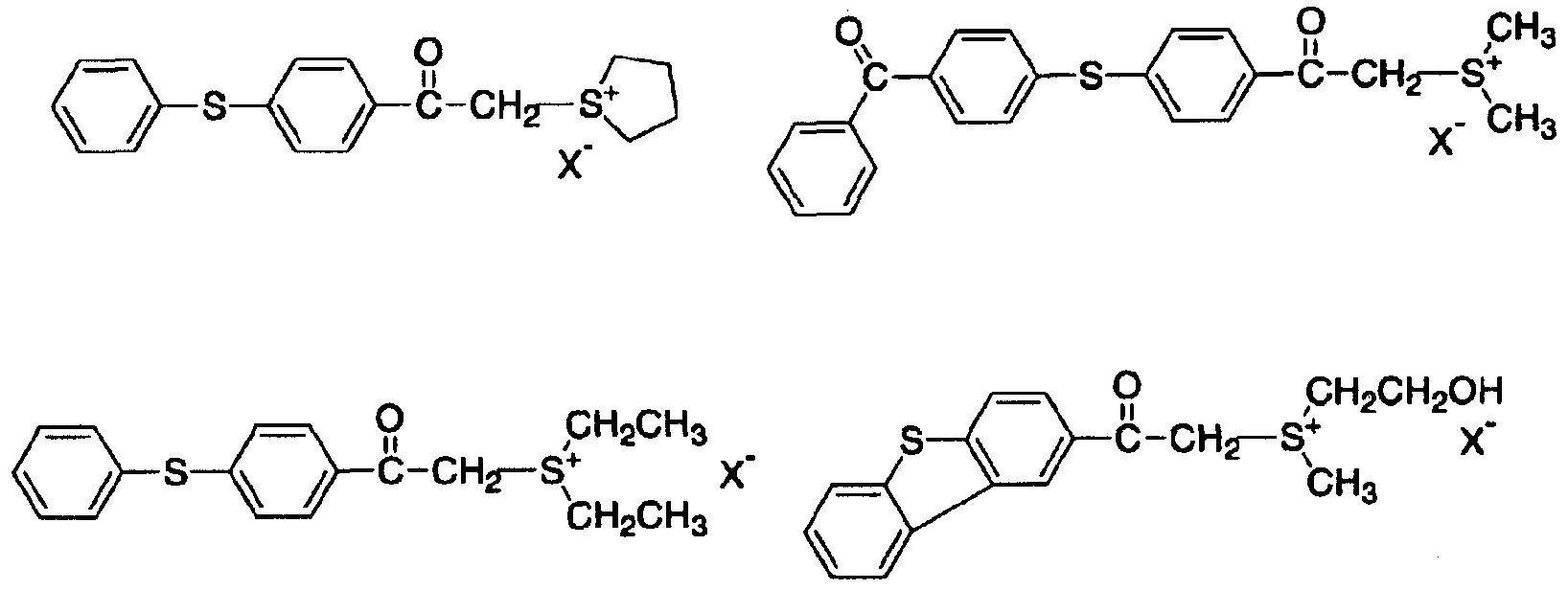


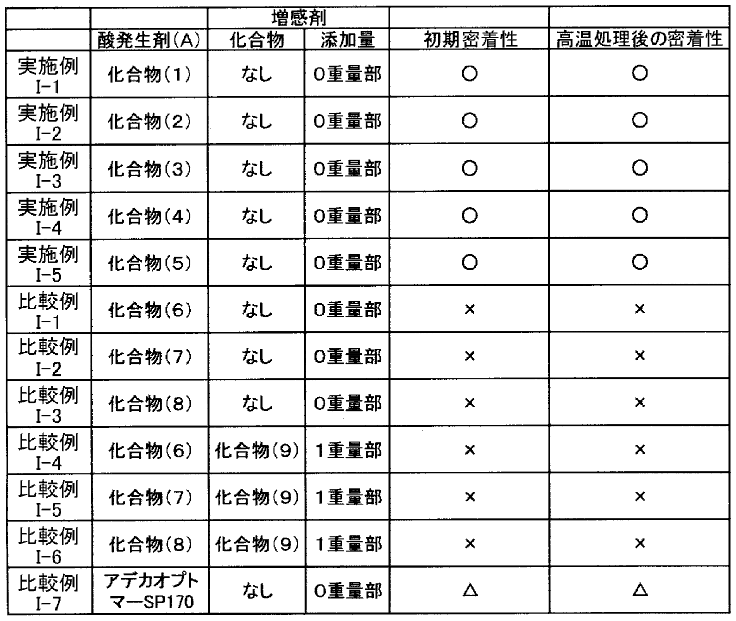


Claims


Priority Applications (2)
| Application Number | Priority Date | Filing Date | Title |
|---|---|---|---|
| US11/575,919 US20080044149A1 (en) | 2004-11-26 | 2005-11-24 | Polymerizable Composition |
| EP05809475A EP1816152A4 (en) | 2004-11-26 | 2005-11-24 | POLYMERIZABLE COMPOSITION |
Applications Claiming Priority (6)
| Application Number | Priority Date | Filing Date | Title |
|---|---|---|---|
| JP2004-341597 | 2004-11-26 | ||
| JP2004341597A JP4929586B2 (ja) | 2004-11-26 | 2004-11-26 | 封止用組成物 |
| JP2004357990A JP4529669B2 (ja) | 2004-12-10 | 2004-12-10 | 光導波路形成用材料、光導波路の製造方法、および光導波路 |
| JP2004-357990 | 2004-12-10 | ||
| JP2005177454A JP2006348199A (ja) | 2005-06-17 | 2005-06-17 | 接着剤組成物およびそれを用いた接着フィルム、接着物の製造方法 |
| JP2005-177454 | 2005-06-17 |
Publications (1)
| Publication Number | Publication Date |
|---|---|
| WO2006057298A1 true WO2006057298A1 (ja) | 2006-06-01 |
Family
ID=36498034
Family Applications (1)
| Application Number | Title | Priority Date | Filing Date |
|---|---|---|---|
| PCT/JP2005/021579 WO2006057298A1 (ja) | 2004-11-26 | 2005-11-24 | 重合性組成物 |
Country Status (6)
| Country | Link |
|---|---|
| US (1) | US20080044149A1 (ja) |
| EP (1) | EP1816152A4 (ja) |
| KR (1) | KR100875566B1 (ja) |
| CN (1) | CN101696273A (ja) |
| TW (1) | TWI392695B (ja) |
| WO (1) | WO2006057298A1 (ja) |
Families Citing this family (8)
| Publication number | Priority date | Publication date | Assignee | Title |
|---|---|---|---|---|
| US7989517B2 (en) * | 2005-11-28 | 2011-08-02 | Konica Minolta Medical & Graphic, Inc. | Actinic ray curable composition, actinic ray curable ink, and image formation process employing the same |
| US8268104B1 (en) * | 2008-03-24 | 2012-09-18 | Hybrid Windshield Repair, LLC | Methods of using UV curing cationic epoxy for windshield repair |
| US20110177259A1 (en) * | 2008-09-01 | 2011-07-21 | Nissan Chemical Industries, Ltd. | Method for manufacturing optical waveguide |
| KR101022030B1 (ko) * | 2009-04-20 | 2011-03-16 | 이미지랩(주) | 저항막 방식 터치 시트 및 이의 제조 방법 |
| KR101265913B1 (ko) * | 2010-06-08 | 2013-05-20 | 세키스이가가쿠 고교가부시키가이샤 | 광 반도체 장치용 다이본드재 및 이를 이용한 광 반도체 장치 |
| JP5939388B2 (ja) * | 2012-05-18 | 2016-06-22 | 株式会社スリーボンド | 硬化性樹脂組成物およびプライマー組成物 |
| KR20200106022A (ko) * | 2018-01-09 | 2020-09-10 | 가부시키가이샤 아데카 | 조성물, 경화물, 광학 필터 및 경화물의 제조 방법 |
| CN114250051B (zh) * | 2021-12-24 | 2023-05-30 | 韦尔通科技股份有限公司 | 一种环氧树脂底部填充胶黏剂及其制备方法和应用 |
Citations (6)
| Publication number | Priority date | Publication date | Assignee | Title |
|---|---|---|---|---|
| JPH09176112A (ja) * | 1995-12-28 | 1997-07-08 | Toyo Ink Mfg Co Ltd | 感エネルギー線酸発生剤、感エネルギー線酸発生剤組成物および硬化性組成物 |
| JPH09194819A (ja) * | 1996-01-16 | 1997-07-29 | Toyo Ink Mfg Co Ltd | 感エネルギー線酸発生剤、感エネルギー線酸発生剤組成物、それを用いた硬化性組成物、およびハイブリッド型硬化性組成物 |
| JPH101508A (ja) * | 1996-06-17 | 1998-01-06 | Toyo Ink Mfg Co Ltd | 感活性線酸発生剤組成物、感応性組成物および画像記録用組成物 |
| JPH107709A (ja) * | 1996-06-24 | 1998-01-13 | Toyo Ink Mfg Co Ltd | 感エネルギー線活性剤組成物、それを用いた感応性組成物ならびに画像形成用組成物 |
| JP2000191751A (ja) * | 1998-12-25 | 2000-07-11 | Sumitomo Bakelite Co Ltd | 紫外線硬化型樹脂組成物 |
| JP2004231938A (ja) * | 2002-09-13 | 2004-08-19 | Sekisui Chem Co Ltd | 有機el素子封止用光硬化性接着剤組成物、有機el素子の封止方法および有機el素子 |
Family Cites Families (9)
| Publication number | Priority date | Publication date | Assignee | Title |
|---|---|---|---|---|
| DE19534954A1 (de) * | 1995-09-20 | 1997-03-27 | Ligmatech Maschb Gmbh | Hochspeicher für Werkstücke und Verfahren zum Betreiben eines Hochspeichers |
| JPH09183961A (ja) * | 1995-12-28 | 1997-07-15 | Toyo Ink Mfg Co Ltd | 感エネルギー線酸発生剤、感エネルギー線酸発生剤組成物、それを用いた硬化性組成物、およびハイブリッド型硬化性組成物 |
| DE59802943D1 (de) * | 1997-06-30 | 2002-03-14 | Siemens Ag | Reaktionsharzmischungen und deren Verwendung |
| ATE258210T1 (de) * | 1997-11-05 | 2004-02-15 | Showa Denko Kk | Photohärtbare farbzusammensetzung für strassenmarkierungen |
| JP2001310938A (ja) * | 2000-04-28 | 2001-11-06 | Showa Denko Kk | 重合性組成物、その硬化物と製造方法 |
| JP2003306655A (ja) * | 2002-04-15 | 2003-10-31 | Toyo Ink Mfg Co Ltd | 硬化型粘接着材料 |
| JP3798417B2 (ja) * | 2002-06-17 | 2006-07-19 | 積水化学工業株式会社 | 有機エレクトロルミネッセンス素子封止用接着剤、有機エレクトロルミネッセンス素子封止用粘着テープ、有機エレクトロルミネッセンス素子封止用両面粘着テープ、有機エレクトロルミネッセンス素子の封止方法、及び、有機エレクトロルミネッセンス素子 |
| JP2005126580A (ja) * | 2003-10-24 | 2005-05-19 | Toyo Ink Mfg Co Ltd | 硬化型粘接着材料 |
| JP4716749B2 (ja) * | 2004-02-20 | 2011-07-06 | 株式会社Adeka | 新規な芳香族スルホニウム塩化合物、これからなる光酸発生剤およびこれを含む光重合性組成物、光学的立体造形用樹脂組成物ならびに光学的立体造形法 |
-
2005
- 2005-11-24 US US11/575,919 patent/US20080044149A1/en not_active Abandoned
- 2005-11-24 KR KR20077006764A patent/KR100875566B1/ko active IP Right Grant
- 2005-11-24 CN CN200910205853A patent/CN101696273A/zh active Pending
- 2005-11-24 EP EP05809475A patent/EP1816152A4/en not_active Withdrawn
- 2005-11-24 WO PCT/JP2005/021579 patent/WO2006057298A1/ja active Application Filing
- 2005-11-25 TW TW094141418A patent/TWI392695B/zh not_active IP Right Cessation
Patent Citations (6)
| Publication number | Priority date | Publication date | Assignee | Title |
|---|---|---|---|---|
| JPH09176112A (ja) * | 1995-12-28 | 1997-07-08 | Toyo Ink Mfg Co Ltd | 感エネルギー線酸発生剤、感エネルギー線酸発生剤組成物および硬化性組成物 |
| JPH09194819A (ja) * | 1996-01-16 | 1997-07-29 | Toyo Ink Mfg Co Ltd | 感エネルギー線酸発生剤、感エネルギー線酸発生剤組成物、それを用いた硬化性組成物、およびハイブリッド型硬化性組成物 |
| JPH101508A (ja) * | 1996-06-17 | 1998-01-06 | Toyo Ink Mfg Co Ltd | 感活性線酸発生剤組成物、感応性組成物および画像記録用組成物 |
| JPH107709A (ja) * | 1996-06-24 | 1998-01-13 | Toyo Ink Mfg Co Ltd | 感エネルギー線活性剤組成物、それを用いた感応性組成物ならびに画像形成用組成物 |
| JP2000191751A (ja) * | 1998-12-25 | 2000-07-11 | Sumitomo Bakelite Co Ltd | 紫外線硬化型樹脂組成物 |
| JP2004231938A (ja) * | 2002-09-13 | 2004-08-19 | Sekisui Chem Co Ltd | 有機el素子封止用光硬化性接着剤組成物、有機el素子の封止方法および有機el素子 |
Non-Patent Citations (1)
| Title |
|---|
| See also references of EP1816152A4 * |
Also Published As
| Publication number | Publication date |
|---|---|
| KR20070056120A (ko) | 2007-05-31 |
| US20080044149A1 (en) | 2008-02-21 |
| EP1816152A1 (en) | 2007-08-08 |
| TW200624459A (en) | 2006-07-16 |
| CN101696273A (zh) | 2010-04-21 |
| KR100875566B1 (ko) | 2008-12-23 |
| EP1816152A4 (en) | 2009-05-06 |
| TWI392695B (zh) | 2013-04-11 |
Similar Documents
| Publication | Publication Date | Title |
|---|---|---|
| JP6578339B2 (ja) | 樹脂組成物 | |
| WO2006057298A1 (ja) | 重合性組成物 | |
| TWI647248B (zh) | Epoxy resin composition, cured product thereof, and curable resin composition | |
| JP4452683B2 (ja) | 有機エレクトロルミネッセンス素子用封止剤、有機エレクトロルミネッセンス表示装置の製造方法、及び、有機エレクトロルミネッセンス表示装置 | |
| JP6560985B2 (ja) | 樹脂組成物 | |
| JP5256570B2 (ja) | 封止用組成物 | |
| JP5072101B2 (ja) | Mems用感光性樹脂組成物及びその硬化物 | |
| JP2006307011A (ja) | エポキシ樹脂、およびエポキシ樹脂組成物 | |
| JP2009259656A (ja) | 封止剤 | |
| KR101685723B1 (ko) | 비닐 에터 단량체를 포함하는 혼합물로 제조된 중합체 | |
| JP7385722B2 (ja) | 封止剤、硬化体、有機エレクトロルミネッセンス表示装置、及び装置の製造方法 | |
| CN112322195B (zh) | 一种紫外光固化组合物胶水及其使用方法和应用 | |
| JP2007045986A (ja) | 接着剤組成物およびそれを用いた接着フィルム、接着物の製造方法 | |
| JP2009079230A (ja) | 有機エレクトロルミネッセンス素子用封止剤、有機エレクトロルミネッセンス表示装置の製造方法、及び、有機エレクトロルミネッセンス表示装置 | |
| JP2009013315A (ja) | 封止用組成物 | |
| JP2006307062A (ja) | エポキシ樹脂組成物及びそれを用いた光学電子部材 | |
| CN1414048A (zh) | 形成保护膜用固化性组合物、该膜的形成方法和该膜 | |
| JP4929586B2 (ja) | 封止用組成物 | |
| JP2006348199A (ja) | 接着剤組成物およびそれを用いた接着フィルム、接着物の製造方法 | |
| CN104918977B (zh) | 环氧树脂、固化性树脂组合物和固化物 | |
| JP2009007502A (ja) | 封止用組成物 | |
| JP2009015085A (ja) | 光導波路形成用材料、光導波路の製造方法、および光導波路 | |
| JP4529669B2 (ja) | 光導波路形成用材料、光導波路の製造方法、および光導波路 | |
| JP4915896B2 (ja) | エポキシ樹脂の製造法 | |
| JP2009013316A (ja) | 接着剤組成物およびそれを用いた接着フィルム、接着物の製造方法 |
Legal Events
| Date | Code | Title | Description |
|---|---|---|---|
| AK | Designated states |
Kind code of ref document: A1 Designated state(s): AE AG AL AM AT AU AZ BA BB BG BR BW BY BZ CA CH CN CO CR CU CZ DE DK DM DZ EC EE EG ES FI GB GD GE GH GM HR HU ID IL IN IS KE KG KM KN KP KR KZ LC LK LR LS LT LU LV LY MA MD MG MK MN MW MX MZ NA NG NI NO NZ OM PG PH PL PT RO RU SC SD SE SG SK SL SM SY TJ TM TN TR TT TZ UA UG US UZ VC VN YU ZA ZM ZW |
|
| AL | Designated countries for regional patents |
Kind code of ref document: A1 Designated state(s): GM KE LS MW MZ NA SD SL SZ TZ UG ZM ZW AM AZ BY KG KZ MD RU TJ TM AT BE BG CH CY CZ DE DK EE ES FI FR GB GR HU IE IS IT LT LU LV MC NL PL PT RO SE SI SK TR BF BJ CF CG CI CM GA GN GQ GW ML MR NE SN TD TG |
|
| 121 | Ep: the epo has been informed by wipo that ep was designated in this application | ||
| WWE | Wipo information: entry into national phase |
Ref document number: 11575919 Country of ref document: US Ref document number: 1020077006764 Country of ref document: KR Ref document number: 200580032200.4 Country of ref document: CN |
|
| WWE | Wipo information: entry into national phase |
Ref document number: 2005809475 Country of ref document: EP |
|
| NENP | Non-entry into the national phase |
Ref country code: DE |
|
| WWP | Wipo information: published in national office |
Ref document number: 2005809475 Country of ref document: EP |
|
| WWP | Wipo information: published in national office |
Ref document number: 11575919 Country of ref document: US |