WO2004034412A1 - 金属化フィルムコンデンサ - Google Patents
金属化フィルムコンデンサ Download PDFInfo
- Publication number
- WO2004034412A1 WO2004034412A1 PCT/JP2003/012949 JP0312949W WO2004034412A1 WO 2004034412 A1 WO2004034412 A1 WO 2004034412A1 JP 0312949 W JP0312949 W JP 0312949W WO 2004034412 A1 WO2004034412 A1 WO 2004034412A1
- Authority
- WO
- WIPO (PCT)
- Prior art keywords
- electrode
- split
- metallikon
- metallized film
- slit
- Prior art date
Links
- 239000003990 capacitor Substances 0.000 title claims abstract description 106
- 239000011104 metalized film Substances 0.000 title claims abstract description 103
- 238000007740 vapor deposition Methods 0.000 claims abstract description 37
- 238000009413 insulation Methods 0.000 claims abstract description 22
- 239000010408 film Substances 0.000 claims description 67
- 230000008021 deposition Effects 0.000 claims description 31
- 239000002184 metal Substances 0.000 claims description 11
- 229910052751 metal Inorganic materials 0.000 claims description 11
- 238000009499 grossing Methods 0.000 claims description 5
- 238000005272 metallurgy Methods 0.000 claims 1
- 230000015572 biosynthetic process Effects 0.000 abstract 1
- 238000010276 construction Methods 0.000 abstract 1
- 238000010438 heat treatment Methods 0.000 abstract 1
- 238000000151 deposition Methods 0.000 description 29
- 230000000694 effects Effects 0.000 description 9
- 230000007423 decrease Effects 0.000 description 8
- 230000020169 heat generation Effects 0.000 description 7
- 230000007547 defect Effects 0.000 description 4
- 239000004743 Polypropylene Substances 0.000 description 3
- 238000005516 engineering process Methods 0.000 description 3
- 239000000463 material Substances 0.000 description 3
- -1 polypropylene Polymers 0.000 description 3
- 229920001155 polypropylene Polymers 0.000 description 3
- 238000011084 recovery Methods 0.000 description 3
- 229910052782 aluminium Inorganic materials 0.000 description 2
- XAGFODPZIPBFFR-UHFFFAOYSA-N aluminium Chemical compound [Al] XAGFODPZIPBFFR-UHFFFAOYSA-N 0.000 description 2
- 238000007664 blowing Methods 0.000 description 2
- 238000011156 evaluation Methods 0.000 description 2
- 239000011888 foil Substances 0.000 description 2
- 238000010030 laminating Methods 0.000 description 2
- 230000007774 longterm Effects 0.000 description 2
- 239000003921 oil Substances 0.000 description 2
- 238000004804 winding Methods 0.000 description 2
- QNRATNLHPGXHMA-XZHTYLCXSA-N (r)-(6-ethoxyquinolin-4-yl)-[(2s,4s,5r)-5-ethyl-1-azabicyclo[2.2.2]octan-2-yl]methanol;hydrochloride Chemical compound Cl.C([C@H]([C@H](C1)CC)C2)CN1[C@@H]2[C@H](O)C1=CC=NC2=CC=C(OCC)C=C21 QNRATNLHPGXHMA-XZHTYLCXSA-N 0.000 description 1
- 241000270295 Serpentes Species 0.000 description 1
- XUIMIQQOPSSXEZ-UHFFFAOYSA-N Silicon Chemical compound [Si] XUIMIQQOPSSXEZ-UHFFFAOYSA-N 0.000 description 1
- UCKMPCXJQFINFW-UHFFFAOYSA-N Sulphide Chemical compound [S-2] UCKMPCXJQFINFW-UHFFFAOYSA-N 0.000 description 1
- 230000015556 catabolic process Effects 0.000 description 1
- 239000003822 epoxy resin Substances 0.000 description 1
- 239000000446 fuel Substances 0.000 description 1
- 238000001465 metallisation Methods 0.000 description 1
- 238000000034 method Methods 0.000 description 1
- 229920000647 polyepoxide Polymers 0.000 description 1
- 229920006395 saturated elastomer Polymers 0.000 description 1
- 229910052710 silicon Inorganic materials 0.000 description 1
- 239000010703 silicon Substances 0.000 description 1
Classifications
-
- H—ELECTRICITY
- H01—ELECTRIC ELEMENTS
- H01G—CAPACITORS; CAPACITORS, RECTIFIERS, DETECTORS, SWITCHING DEVICES, LIGHT-SENSITIVE OR TEMPERATURE-SENSITIVE DEVICES OF THE ELECTROLYTIC TYPE
- H01G4/00—Fixed capacitors; Processes of their manufacture
- H01G4/002—Details
- H01G4/228—Terminals
-
- H—ELECTRICITY
- H01—ELECTRIC ELEMENTS
- H01G—CAPACITORS; CAPACITORS, RECTIFIERS, DETECTORS, SWITCHING DEVICES, LIGHT-SENSITIVE OR TEMPERATURE-SENSITIVE DEVICES OF THE ELECTROLYTIC TYPE
- H01G2/00—Details of capacitors not covered by a single one of groups H01G4/00-H01G11/00
- H01G2/14—Protection against electric or thermal overload
- H01G2/16—Protection against electric or thermal overload with fusing elements
-
- H—ELECTRICITY
- H01—ELECTRIC ELEMENTS
- H01G—CAPACITORS; CAPACITORS, RECTIFIERS, DETECTORS, SWITCHING DEVICES, LIGHT-SENSITIVE OR TEMPERATURE-SENSITIVE DEVICES OF THE ELECTROLYTIC TYPE
- H01G4/00—Fixed capacitors; Processes of their manufacture
- H01G4/002—Details
- H01G4/005—Electrodes
- H01G4/012—Form of non-self-supporting electrodes
-
- H—ELECTRICITY
- H01—ELECTRIC ELEMENTS
- H01G—CAPACITORS; CAPACITORS, RECTIFIERS, DETECTORS, SWITCHING DEVICES, LIGHT-SENSITIVE OR TEMPERATURE-SENSITIVE DEVICES OF THE ELECTROLYTIC TYPE
- H01G4/00—Fixed capacitors; Processes of their manufacture
- H01G4/002—Details
- H01G4/018—Dielectrics
- H01G4/06—Solid dielectrics
- H01G4/14—Organic dielectrics
- H01G4/145—Organic dielectrics vapour deposited
-
- H—ELECTRICITY
- H01—ELECTRIC ELEMENTS
- H01G—CAPACITORS; CAPACITORS, RECTIFIERS, DETECTORS, SWITCHING DEVICES, LIGHT-SENSITIVE OR TEMPERATURE-SENSITIVE DEVICES OF THE ELECTROLYTIC TYPE
- H01G4/00—Fixed capacitors; Processes of their manufacture
- H01G4/002—Details
- H01G4/228—Terminals
- H01G4/252—Terminals the terminals being coated on the capacitive element
Definitions
- the present invention relates to a metallized film capacitor used for electronic equipment, electric equipment, industrial equipment, and automobiles. Background art
- Metallized film capacitors are generally classified into those that use metal foil for the electrodes and those that use the metal deposited on the dielectric film for the electrodes. Above all, metallized film capacitors that use a metal deposited as an electrode (hereinafter, referred to as a vapor-deposited electrode) require a smaller volume and smaller weight than those that use a metal foil as an electrode. It has been widely used because it has high recovery performance and high reliability against insulation rupture.
- the self-healing performance refers to the ability to recover the function of a capacitor when short-circuiting occurs at an insulation defect and the vaporized electrode around the defect evaporates and scatters due to the energy of the short-circuit.
- Conventional examples 1 to 3 of such a metallized film capacitor are shown in FIGS.
- one of the metallized films has a deposition electrode 110 formed by depositing a metal on one surface of a dielectric film 3a except for an insulating margin 4a at one end. Further, the deposition electrode 110 has a plurality of divided electrodes 2a divided by a non-deposition slit 52a having no deposition metal, and is not divided through a fuse 7a provided in the slit 52a. It is connected in parallel to electrode 1a. On the other side of the metallized film, a vapor deposition electrode 210 is formed on one surface of the dielectric film 3b except for the insulation margin 4b at the end opposite to the insulation margin 4a, and is formed on the other surface. It is divided electrode 1b.
- the two metallized films are wound and wound so that the insulation margins 4a and 4b do not overlap, or after alternately laminating a plurality of films, the metallized film 110
- the connecting portion is formed by forming the silicon 6a on the metallization 6a and the metallikon 6b on the vapor deposition electrode 210.
- Figures 15 and 16A and 16B show the insulation margin 78a.
- the self-healing performance is better as the thickness of the deposition electrodes 110 and 210 is smaller, and the deposition electrodes are scattered with less energy. Therefore, as shown in FIG. 15, for example, as shown by the width W, the thickness of the vapor deposition electrode of the effective electrode portion 2a that forms the capacitance is reduced, and the vapor deposition electrode 1 is formed at the portion connected to the metallikons 6a and 6b.
- a heavy-edge structure having a thick-film electrode portion 11a having a thickness of 10 is also widely used. With this structure, the withstand voltage of the capacitor can be increased and a high potential gradient can be achieved.
- the deposition electrode portion into a plurality of divided electrodes 2a by slits 52a where no metal is provided, and provide a fuse 7a in a part of the slits 52a to connect the divided electrodes in parallel. Is being done. This is to secure the self-protection function of blowing the fuse 7a near the insulation defect and disconnecting the insulation defect from the electric circuit by the short-circuit current at the time of the self-recovery described above.
- a grid-like divided electrode 32a is also proposed in which 2a is provided in a grid shape, the deposition electrodes are finely divided, and each is connected in parallel with a fuse 7a. With this method, the split electrode
- the area of 32a is small, the decrease in capacity when the fuse 7a is blown is small. Further, it is stated that by limiting the shape of the fuse and the area of each of the divided electrodes 32a to a predetermined range, the insulation recovery performance of the vapor deposition electrode can be improved, so that a higher potential gradient can be achieved.
- increasing the potential gradient means increasing the withstand voltage per ⁇ ⁇ thickness of the dielectric film. .
- Japanese Patent Application Laid-Open No. Hei 4-252508 discloses that a grid-like divided electrode having a rounded free end of a divided slit has a potential twice as high as a metallized film capacitor without a divided electrode. It discloses that a gradient can be obtained.
- Japanese Patent Application Laid-Open No. 5-132921 discloses a metallized film capacitor composed of grid-like divided electrodes. It discloses that a metallized film capacitor having a DC potential gradient of 130 to 350 ⁇ can be realized when the area of the split electrode is 10 to 100 mm 2 .
- the number of fuses is increased, so that the temperature rise is further increased.
- the withstand voltage and long-term reliability were greatly reduced.
- the problem to be solved by the present invention is to reduce the heat generated by the fuse at the time of energization, suppress the temperature rise of the capacitor, and improve the withstand voltage of the metallized film capacitor.
- the present invention relates to a metallized film capacitor having a self-security function, wherein a pair of vapor-deposited electrodes are formed as divided electrodes connected on the side close to an insulating magazine by a fuse. is there.
- the current flowing through one of the deposition electrodes decreases as approaching the insulation margin, so that the current flowing through the fuse can be reduced to reduce heat generation. Furthermore, on the side facing away from the insulation magazine, because the other deposition electrode is divided and has a fuse, no matter where the effective electrode section is short-circuited, the fuse is blown and the electrical circuit is disconnected. It is possible to form a self-security function to separate.
- the present invention generates a large amount of heat when the effective electrode portion of the deposition electrode on the side facing the insulating magazine is divided into a grid shape, compared to the conventional technology in which the deposition electrode is uniformly divided into a grid shape. Can be reduced.
- the present invention can greatly reduce heat generation even when the side facing the insulation margin is divided by using a deposition electrode having a snake edge structure.
- FIG. 1 is a cross-sectional view of a metalized film capacitor according to Embodiment 1 of the present invention.
- FIG. 2A is a plan view of one metalized film according to Embodiment 1 of the present invention.
- FIG. 2B is a plan view of the other metallized film according to Embodiment 1 of the present invention.
- FIG. 3 is a cross-sectional view of a metallized film capacitor according to Embodiment 2 of the present invention.
- FIG. 4A is a plan view of one metallized film according to Embodiment 2 of the present invention.
- FIG. 4B is a plan view of the other metallized film according to Embodiment 2 of the present invention.
- FIG. 5 is a sectional view of a metallized film capacitor according to Embodiment 3 of the present invention.
- FIG. 6A is a plan view of a vapor deposition electrode on one surface of a metallized film according to Embodiment 3 of the present invention.
- FIG. 6B is a plan view of a deposition electrode on the other surface of the metallized film according to Embodiment 3 of the present invention. 2949
- FIG. 7 is a cross-sectional view of a metallized film capacitor according to Embodiment 4 of the present invention.
- FIG. 8A is a plan view of one metalized film according to Embodiment 4 of the present invention.
- FIG. 8B is a plan view of the other metallized film according to Embodiment 4 of the present invention.
- FIG. 9 is a cross-sectional view of a metalized film capacitor according to Embodiment 5 of the present invention.
- FIG. 1OA is a plan view of one metalized film according to Embodiment 5 of the present invention.
- FIG. 10B is a plan view of the other metallized film according to Embodiment 5 of the present invention.
- FIG. 11 is a cross-sectional view of a metallized film capacitor in Conventional Example 1.
- FIG. 12A is a plan view of one metalized film in Conventional Example 1.
- FIG. 12A is a plan view of one metalized film in Conventional Example 1.
- FIG. 12B is a plan view of the other metallized film in Conventional Example 1.
- FIG. 13 is a cross-sectional view of a metallized film capacitor in Conventional Example 2.
- FIG. 14A is a plan view of one metallized film in Conventional Example 2.
- FIG. 14A is a plan view of one metallized film in Conventional Example 2.
- FIG. 14B is a plan view of the other metallized film in Conventional Example 2.
- FIG. 15 is a cross-sectional view of a metallized film capacitor in Conventional Example 3.
- FIG. 16A is a plan view of one metallized film in Conventional Example 3.
- FIG. 16B is a plan view of the other metallized film in Conventional Example 3. BEST MODE FOR CARRYING OUT THE INVENTION
- FIGS. 1 and 2A and 2B show a first metal film 100 and a second metallized film 200 which form a wound-type metallized film capacitor.
- the one metallized film 100 and the second metallized film 200 are a pair of vapor-deposited electrodes 110, 210 formed by pattern-depositing aluminum on one side of the dielectric films 3a, 3. It has insulating magazines 4a and 4b provided at one end, and the electrodes are drawn out from a pair of vapor deposition electrodes 110 and 210 through metallikons 6a and 6b provided at both end surfaces.
- the vapor deposition electrodes 110 and 210 have non-vapor deposition slits 5a and 5b having no vapor deposition electrode substantially at the center of the width W of the effective electrode portion forming the capacitance.
- the slits 5a and 5b are created by transferring patterned oil onto a dielectric film before vapor deposition. Further, as shown in FIGS. 2A and 2B, the vapor deposition electrodes 110 and 210 are located on the insulating margins 4a and 4b sides with the slits 5a and 5b at the approximate center of the width W of the effective electrode portion.
- It has a plurality of divided electrodes 2a, 2b, and has non-divided electrodes 1a, lb on the side of metallikons 6a, 6b.
- the split electrodes 2a and 2b are split by slits 52a and 52b.
- the split electrode 2a and the non-split electrode 1a and the split electrode 2b and the non-split electrode 1b are connected in parallel by fuses 7a and 7b, respectively.
- the current flowing through the vapor deposition electrodes 110 and 210 is larger near the metallikons 6a and 6b, and smaller the farther away. Therefore, the vapor deposition electrodes 110 and 210 on the side close to the metallikons 6a and 6b are formed without being divided over one entire surface of the dielectric films 3a and 3b in accordance with the magnitude of the flowing current.
- the split electrodes 2a and 2b and the fuses 7a and 7b are provided in the electrode portion located far from the metallikons 6a and 6b and having a small amount of flowing current. With this configuration, heat generated by the fuses 7a and 7b due to flowing current can be reduced, and a temperature rise can be suppressed.
- the second embodiment is different from the first embodiment in that the deposition electrode on the side from the approximate center of the width of the effective electrode portion toward the insulating margin is formed as a grid-shaped divided electrode. Portions having the same configuration and the same function and effect as those of the first embodiment are denoted by the same reference numerals, and different points will be mainly described.
- the vapor deposition electrodes 110 and 210 have a slit 5 at almost the center of the width W of the effective electrode portion forming the capacitance. a, 5b with insulation margins 4a, 4b from the center
- the slits 52 a and 52 b having no vapor deposition electrodes are provided on the side facing toward them.
- the plurality of grid-like divided electrodes 32a and 32b are divided by 52a and 52b, and they are connected in parallel by fuses 7a and 7b.
- non-split electrodes 1a and 1b are provided on the sides adjacent to the metallikons 6a and 6b with the slits 5a and 5b at the center therebetween.
- the vapor deposition electrodes 110, 210 are thinner than the vapor deposition electrodes 110, 210 in the effective electrode portion, and are located at portions where the metal electrodes 6a, 6b are connected.
- a so-called heavy edge structure having a configuration having the thick film electrode portions 11a and 11b was adopted.
- Embodiment 3 is different from Embodiment 1 in that a pair of vapor-deposited electrodes are provided on both surfaces of one dielectric film, and no metal is vapor-deposited on the other dielectric film. Portions having the same configuration and the same operation and effect as those of the first embodiment are denoted by the same reference numerals, and different portions will be mainly described.
- the metallized film capacitor of the third embodiment has a dielectric film 53 a having vapor-deposited electrodes 110 and 210 formed on both surfaces, and a non-vapor-deposited film. And the deposition electrodes 110 and 210 are connected to metallikons 6a and 6b formed on both end surfaces. Then, the deposition electrodes 110 and 210 have slits 5a and 5b at substantially the center of the width W of the effective electrode portion forming the capacitance, and extend from the center to the insulating margins 4a and 4b.
- the side is divided into a plurality of grid-like divided electrodes 32a, 32b by slits 52a, 52b without vapor deposition electrodes, respectively, and connected in parallel by fuses 7a, 7b.
- non-divided electrodes 1a and lb are provided on the sides adjacent to the metallikons 6a and 6b with the central portion interposed therebetween.
- the deposition electrodes 110 and 210 had a heavy edge structure having thick film electrode portions 11a and 11b. According to this configuration, the same operation and effect as described in the first embodiment can be obtained, and the deposition electrodes 110 and 210 can be formed in one deposition step.
- a metallized film capacitor can be manufactured at lower cost.
- the metallized film capacitors shown in Embodiments 1 to 3 of the present invention are manufactured by winding an oval-shaped capacitor element formed by winding a 4 jum-thick polypropylene film as a dielectric film, using a PPS (Bolifen Elenylene Sulfide). After being put in a case, it is molded with epoxy resin.
- the electric capacity of the oval capacitor element is 120 / JF.
- the width W of the effective electrode portion was set to 80 mm, and the width of each of the fuses 7a and 7b was set to 0.4 mm.
- metallized film capacitors manufactured using the conventional technology are shown in Conventional Examples 1 and 2.
- the material, thickness, capacity, width W of the effective electrode portion, and width of the fuse of the conventional dielectric film were set to the same values as in the first to third embodiments.
- the split electrode 2a is provided on the dielectric film 3a over the entire width W of the effective electrode portion, and no split electrode is provided on the dielectric film 3b.
- This is a metallized film capacitor provided with a metallized electrode 1b.
- grid-type split electrodes 32 are provided on the dielectric film 3a over the entire width W of the effective electrode section, and split on the dielectric film 3b.
- This is a metallized film capacitor provided with no deposition electrode 3b.
- Each metallized film capacitor produced in this way was supplied with a sinusoidal current with an effective value of 2 OA at 85 kHz at 180 kHz for 180 minutes, and an oval capacitor element was applied. The surface temperature rise was measured. The temperature rise was saturated after 180 minutes in each of the metallized film capacitors. Table 1 shows the obtained results. table 1
- the breakdown voltage of the dielectric film dropped, and fuse fusing occurred in many places due to local short circuits.
- the heat generated by the ripple current is suppressed, so that the blowing of the fuse is reduced.
- Embodiment 4 is different from Embodiment 1 in that the pair of vapor deposition electrodes is improved. Portions having the same configuration and the same operation and effect as those of the first embodiment are denoted by the same reference numerals, and different points will be mainly described.
- the deposition electrode 110 provided on the dielectric film 3a is positioned substantially at the center thereof in the longitudinal direction of the dielectric film 3a (dielectric film). It is separated into different potentials by an insulation margin 7 8a extending in the longitudinal direction of the lum.
- a slit 5a is provided at the approximate center of the width W of the effective electrode portion, and a plurality of divided electrodes 2a divided by the slits 52a are provided on the side from the center to the insulation margin 78a. And connected in parallel to the non-split electrode 1a on the side near the metallikons 6a and 6b via the fuse 7a.
- the vapor deposition electrode 210 provided on the dielectric film 3b has an insulating margin 4b extending in the longitudinal direction at both ends, and a slit 5b is provided at a substantially central portion of the width W of the effective electrode portion.
- a plurality of divided electrodes 2b separated by slits 5b are provided on the side from the center toward the insulating margin 4b, and a non-electrode located between the divided electrodes 2b on both sides via a fuse 7b. It is connected in parallel to the split electrode 1b.
- the metallikons 6 a and 6 b are connected to the deposition electrodes 110 at both ends of the first metallized film 100.
- the vapor deposition electrode 110 in addition to obtaining the same operation and effect as described in the first embodiment, in addition to the insulating margin 7 extending in the longitudinal direction of the dielectric film 3a, the vapor deposition electrode 110 can be obtained. Since the two unit capacitors separated to the left and right by 8a are connected in series, it is possible to use a higher voltage, and it has a self-protection function, and the metalized film that generates less heat due to the fuse 7a Capacitor can be realized.
- the fifth embodiment is different from the fourth embodiment in that a pair of deposition electrodes is configured as a grid-like divided electrode. Portions having the same configuration and the same function and effect as those of the first embodiment are denoted by the same reference numerals, and different portions will be mainly described.
- the vapor deposition electrode 110 is separated into different potentials by an insulating mag- net 78a, and a slit 5a is formed at almost the center of the width W of the effective electrode portion.
- a slit 5a is formed at almost the center of the width W of the effective electrode portion.
- the vapor deposition electrode 210 also has a slit 5b at substantially the center of the width W of the effective electrode portion, and extends from the center toward the insulation margin 4b located at both ends of the dielectric film 3b.
- the same operation and effect as described in the first embodiment can be obtained.
- two unit capacitors are connected in series. Since the heat generation of the electrode 32b is also suppressed, a metallized film capacitor having a high potential gradient and low heat generation can be realized.
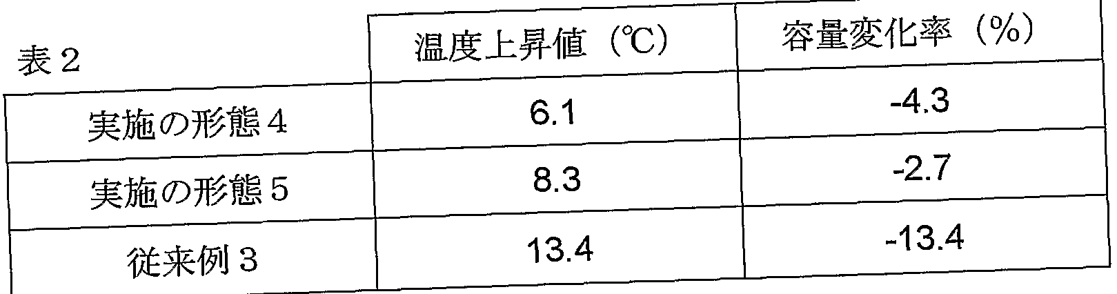
- the metallized film capacitors according to Embodiments 4 and 5 were wound using a polypropylene film having a thickness of 3.2 ⁇ as the dielectric films 3 a and 3 b having the deposition electrodes 110 and 210.
- a round 6 O y F round capacitor element is housed in an aluminum cylindrical case and impregnated with insulating oil.
- the width W of the effective electrode portion was 5 O mm, and the width of each of the fuses 7a and 7b was 0.4 mm.
- a metallized film capacitor of the prior art was manufactured in Conventional Example 3.
- the material, thickness, capacitance, effective electrode width, and fuse width of the dielectric film of Conventional Example 3 were set to the same values as in Embodiments 4 and 5.
- the dielectric film 3a is provided with an insulating margin 78a and a divided electrode 2a covering the entire width W of the effective electrode section.
- 3b is a metallized film capacitor provided with undivided electrodes 1b without division.
- a sine wave current with an effective value of 15 A at 85 kHz and an effective value of 15 A was applied to each of the metallized film capacitors thus manufactured at 85 D for 180 minutes in the same manner as described above, and the surface of the round capacitor element was exposed. was measured. Further, with the ripple current flowing at 85 ports, a DC voltage of 130 V was applied, and the capacity change rate after 1000 hours was measured. Table 2 shows the results.
- the metallized film capacitors described in Embodiments 1 to 5 described above are applicable to an electric vehicle using an electric motor as a driving source, and a hybrid vehicle using an engine using gasoline or the like as a fuel and an electric motor as driving sources. It can be used as a smoothing capacitor in an inverter control device that controls the rotation speed of the electric motor mounted on the vehicle. In other words, the heat generated by the fuse during current flow is small, and the decrease in capacity is small, making it ideal for mounting on vehicles with high ambient operating temperatures.
- the insulation margin 78 a is one has been described, but the present invention is not limited to one. Further, in each of the above embodiments, the power described as an example of a rectangular divided electrode is not limited to this.
- the present invention is not limited to this, and other shapes such as a rhombic shape, a hexagonal shape, and a triangular grid-shaped divided electrode Also obtained similar results. Further, the position of the fuse is provided on each side of the square, but may be provided at the top.
- the example has been described in which the same slits 5a and 5b are provided in the longitudinal direction and the width direction of the film, but these widths may be different.
- the example in which the polypropylene film is used for the dielectric films 3a, 3b, 53a or 53b has been described, but similar results can be obtained by using films of other materials. The same effect can be obtained even if two or more films are stacked as the dielectric films 3a and 3b, 53a and 53b, respectively.
- the features of the metallized film capacitor of the present invention have the following features: (1) It has a self-security function and generates less heat in the fuse part. (2) High potential gradient is possible. (3) Withstand voltage can be increased and high potential gradient can be achieved. (4) One pair of deposition electrodes can be provided in one deposition step. (5) The capacity decrease is small.
- the present invention can be applied as a capacitor for a vehicle having a high use environment temperature to a motor controller that controls the speed of an electric motor that is a driving source of the vehicle.
Landscapes
- Engineering & Computer Science (AREA)
- Power Engineering (AREA)
- Microelectronics & Electronic Packaging (AREA)
- Manufacturing & Machinery (AREA)
- Fixed Capacitors And Capacitor Manufacturing Machines (AREA)
Abstract
Description

Claims
Priority Applications (2)
| Application Number | Priority Date | Filing Date | Title |
|---|---|---|---|
| EP03751405A EP1548767B1 (en) | 2002-10-10 | 2003-10-09 | Metallized film capacitor |
| US10/529,551 US7027286B2 (en) | 2002-10-10 | 2003-10-09 | Metallized film capacitor |
Applications Claiming Priority (2)
| Application Number | Priority Date | Filing Date | Title |
|---|---|---|---|
| JP2002297278A JP3914854B2 (ja) | 2002-10-10 | 2002-10-10 | 金属化フィルムコンデンサとそれを用いたインバータ平滑用コンデンサと自動車用コンデンサ |
| JP2002/297278 | 2002-10-10 |
Publications (1)
| Publication Number | Publication Date |
|---|---|
| WO2004034412A1 true WO2004034412A1 (ja) | 2004-04-22 |
Family
ID=32089262
Family Applications (1)
| Application Number | Title | Priority Date | Filing Date |
|---|---|---|---|
| PCT/JP2003/012949 WO2004034412A1 (ja) | 2002-10-10 | 2003-10-09 | 金属化フィルムコンデンサ |
Country Status (5)
| Country | Link |
|---|---|
| US (1) | US7027286B2 (ja) |
| EP (1) | EP1548767B1 (ja) |
| JP (1) | JP3914854B2 (ja) |
| CN (1) | CN100514517C (ja) |
| WO (1) | WO2004034412A1 (ja) |
Cited By (3)
| Publication number | Priority date | Publication date | Assignee | Title |
|---|---|---|---|---|
| WO2007139165A1 (ja) * | 2006-05-31 | 2007-12-06 | Soshin Electric Co., Ltd. | フィルムコンデンサ |
| US7697261B2 (en) * | 2005-04-08 | 2010-04-13 | Panasonic Corporation | Metalized film capacitor and inverter smoothing capacitor for automobile |
| US7929271B2 (en) | 2006-04-28 | 2011-04-19 | Soshin Electric Co., Ltd. | Film capacitor |
Families Citing this family (40)
| Publication number | Priority date | Publication date | Assignee | Title |
|---|---|---|---|---|
| WO2006109732A1 (ja) * | 2005-04-08 | 2006-10-19 | Matsushita Electric Industrial Co., Ltd. | 金属化フィルムコンデンサ及びこれを用いたケースモールド型コンデンサ並びにインバータ回路及び車両駆動用モータの駆動回路 |
| JP2007053222A (ja) * | 2005-08-18 | 2007-03-01 | Matsushita Electric Ind Co Ltd | 金属化フィルムコンデンサ |
| JP5025924B2 (ja) * | 2005-08-18 | 2012-09-12 | パナソニック株式会社 | 金属化フィルムコンデンサ |
| DE102006019124B4 (de) * | 2006-04-25 | 2012-08-30 | Fraunhofer-Gesellschaft zur Förderung der angewandten Forschung e.V. | Bilderfassungssystem zur Rundumsicht |
| JP4893399B2 (ja) * | 2007-03-19 | 2012-03-07 | パナソニック株式会社 | 金属化フィルムコンデンサ |
| JP4957308B2 (ja) * | 2007-03-19 | 2012-06-20 | パナソニック株式会社 | 金属化フィルムコンデンサ |
| KR100836567B1 (ko) | 2007-03-22 | 2008-06-10 | 주식회사 뉴인텍 | 필름 커패시터용 금속화 플라스틱필름 및 필름 커패시터 |
| US20090154056A1 (en) * | 2007-12-17 | 2009-06-18 | General Electric Company | Low inductance capacitor and method of manufacturing same |
| US8427807B2 (en) * | 2008-01-07 | 2013-04-23 | Siemens Aktiengesellschaft | Capacitor for application in high pressure environments |
| JP5012515B2 (ja) * | 2008-01-07 | 2012-08-29 | パナソニック株式会社 | 金属化フィルムコンデンサ |
| US20090225491A1 (en) * | 2008-03-04 | 2009-09-10 | Hui-Chuan Yao | Metallized film capacitor |
| JP5548343B2 (ja) * | 2008-04-28 | 2014-07-16 | 株式会社指月電機製作所 | 金属化フィルムコンデンサ |
| US8593781B2 (en) * | 2009-02-05 | 2013-11-26 | Nichicon Corporation | Metalized film capacitor |
| JP5294123B2 (ja) * | 2009-05-25 | 2013-09-18 | 株式会社指月電機製作所 | 金属化フィルムコンデンサ |
| WO2011055517A1 (ja) | 2009-11-04 | 2011-05-12 | パナソニック株式会社 | 金属化フィルムコンデンサ及びこれを用いたケースモールド型コンデンサ |
| JP2012110109A (ja) * | 2010-11-16 | 2012-06-07 | Omron Corp | パワーコンディショナにおける出力段フィルムコンデンサ構造 |
| WO2012121256A1 (ja) * | 2011-03-10 | 2012-09-13 | 東レ株式会社 | 二軸延伸ポリプロピレンフィルム、金属化フィルム、およびフィルムコンデンサ |
| KR101206872B1 (ko) | 2011-05-11 | 2012-12-04 | 성호전자(주) | 금속화 플라스틱필름과 이의 제조방법 및 이를 이용한 필름 콘덴서 |
| EP2717281B1 (en) | 2011-05-30 | 2019-07-10 | Panasonic Intellectual Property Management Co., Ltd. | Metalized film capacitor |
| CN106783170B (zh) * | 2011-11-11 | 2018-08-24 | 松下知识产权经营株式会社 | 薄膜电容器 |
| US9318262B2 (en) * | 2012-01-06 | 2016-04-19 | Panasonic Intellectual Property Management Co., Ltd. | Film capacitor |
| JP6040592B2 (ja) * | 2012-06-28 | 2016-12-07 | パナソニックIpマネジメント株式会社 | 金属化フィルムコンデンサ |
| JP6330139B2 (ja) * | 2013-11-29 | 2018-05-30 | パナソニックIpマネジメント株式会社 | 金属化フィルムコンデンサ |
| JP2015115362A (ja) * | 2013-12-09 | 2015-06-22 | 小島プレス工業株式会社 | 金属化フィルムコンデンサ |
| CN103779078B (zh) * | 2014-01-15 | 2016-09-21 | 佛山市顺德区胜业电气有限公司 | 一种薄膜电容器用金属化安全膜 |
| US9570239B2 (en) * | 2014-09-02 | 2017-02-14 | Samhwa Capacitor Co., Ltd. | Electrode forming film and film capacitor using the same |
| US9418791B1 (en) * | 2014-10-17 | 2016-08-16 | Black Night Enterprises, Inc. | Folded stack segmented film capacitor |
| CN106024386A (zh) * | 2015-03-31 | 2016-10-12 | 三和电容器株式会社 | 电极形成膜及利用其的薄膜电容器 |
| JP2017059612A (ja) * | 2015-09-15 | 2017-03-23 | パナソニックIpマネジメント株式会社 | 金属化フィルムコンデンサ |
| US10650965B2 (en) | 2016-04-27 | 2020-05-12 | Kyocera Corporation | Film capacitor, combination type capacitor, and inverter and electric vehicle using the same |
| KR101987781B1 (ko) * | 2017-09-05 | 2019-06-12 | 삼화콘덴서공업 주식회사 | 금속화 필름 커패시터 |
| US11631545B2 (en) * | 2017-10-27 | 2023-04-18 | Kyocera Corporation | Film capacitor, combination type capacitor, and inverter and electric vehicle employing the same |
| CN111448631B (zh) * | 2018-01-18 | 2021-12-03 | 松下知识产权经营株式会社 | 薄膜电容器 |
| JP7193070B2 (ja) | 2018-02-05 | 2022-12-20 | 株式会社指月電機製作所 | フィルムコンデンサ |
| WO2019150839A1 (ja) | 2018-02-05 | 2019-08-08 | 株式会社指月電機製作所 | フィルムコンデンサ |
| WO2021085219A1 (ja) * | 2019-10-30 | 2021-05-06 | 京セラ株式会社 | フィルムコンデンサ素子 |
| CN114846568A (zh) * | 2019-12-13 | 2022-08-02 | 京瓷株式会社 | 电介质薄膜、使用该电介质薄膜的薄膜电容器、连结型电容器、逆变器及电动车辆 |
| DE112022003846T5 (de) | 2021-08-06 | 2024-05-23 | Panasonic Intellectual Property Management Co., Ltd. | Folienkondensator |
| CN113643896B (zh) * | 2021-09-10 | 2023-04-18 | 宁波海融电器有限公司 | 内串式电容器安全膜 |
| JPWO2023053911A1 (ja) * | 2021-09-30 | 2023-04-06 |
Citations (7)
| Publication number | Priority date | Publication date | Assignee | Title |
|---|---|---|---|---|
| JPS508050A (ja) * | 1973-04-13 | 1975-01-28 | ||
| JPS61188920A (ja) * | 1985-02-16 | 1986-08-22 | 松下電器産業株式会社 | 金属化フイルムコンデンサ |
| JPS648721U (ja) * | 1987-07-06 | 1989-01-18 | ||
| JPH08288171A (ja) * | 1995-04-19 | 1996-11-01 | Matsushita Electric Ind Co Ltd | 金属化フィルムコンデンサ |
| JPH09199371A (ja) | 1996-01-16 | 1997-07-31 | Matsushita Electric Ind Co Ltd | 金属化フィルムコンデンサ |
| JPH10135072A (ja) * | 1996-10-31 | 1998-05-22 | Hitachi Aic Inc | 金属化フィルムコンデンサ |
| JP2002504747A (ja) * | 1998-02-17 | 2002-02-12 | エプコス アクチエンゲゼルシャフト | 自己回復型シートコンデンサのための金属化部 |
Family Cites Families (12)
| Publication number | Priority date | Publication date | Assignee | Title |
|---|---|---|---|---|
| JPS56101732A (en) * | 1980-01-18 | 1981-08-14 | Matsushita Electric Ind Co Ltd | Metallized film condenser |
| JPS648721A (en) | 1987-07-01 | 1989-01-12 | Mitsubishi Electric Corp | Logic circuit |
| JPH0272609A (ja) * | 1988-09-07 | 1990-03-12 | Marcon Electron Co Ltd | Shコンデンサ |
| DE4010753C1 (ja) | 1990-04-03 | 1991-12-05 | Steiner Gmbh & Co. Kg, 5927 Erndtebrueck, De | |
| JP2993785B2 (ja) | 1991-11-12 | 1999-12-27 | 株式会社加藤製作所 | 自走型クレーンのフック係止構造 |
| US5608600A (en) * | 1993-02-19 | 1997-03-04 | Electronic Concepts Inc. | Metallized film capacitor with increased dielectric breakdown voltage |
| GB2276765B (en) * | 1993-03-30 | 1996-10-09 | Dilipkumar Varma | Metalised film capacitor |
| US5630922A (en) * | 1995-12-26 | 1997-05-20 | Ppg Industries, Inc. | Electrodepositable coating composition containing diorganotin dicarboxylates |
| DE19734477B4 (de) * | 1996-08-09 | 2005-11-03 | Matsushita Electric Industrial Co., Ltd., Kadoma | Metallisierter Filmkondensator und Vorrichtung und Verfahren für die Herstellung eines metallisierten Films für den metallisierten Filmkondensator |
| JP3935561B2 (ja) * | 1997-07-04 | 2007-06-27 | ニチコン株式会社 | 金属化フィルムコンデンサ |
| SE515894C2 (sv) * | 2000-01-14 | 2001-10-22 | Abb Ab | Kondensatorelement för en kraftkondensator, kraftkondensator innefattande dylikt kondensatorelement samt metalliserat band för en kraftkondensator |
| US6954349B2 (en) * | 2001-06-08 | 2005-10-11 | Matsushita Electric Industrial Co., Ltd. | Metallized film capacitor |
-
2002
- 2002-10-10 JP JP2002297278A patent/JP3914854B2/ja not_active Expired - Lifetime
-
2003
- 2003-10-09 CN CNB2003801010617A patent/CN100514517C/zh not_active Ceased
- 2003-10-09 EP EP03751405A patent/EP1548767B1/en not_active Expired - Lifetime
- 2003-10-09 WO PCT/JP2003/012949 patent/WO2004034412A1/ja active Application Filing
- 2003-10-09 US US10/529,551 patent/US7027286B2/en not_active Expired - Lifetime
Patent Citations (7)
| Publication number | Priority date | Publication date | Assignee | Title |
|---|---|---|---|---|
| JPS508050A (ja) * | 1973-04-13 | 1975-01-28 | ||
| JPS61188920A (ja) * | 1985-02-16 | 1986-08-22 | 松下電器産業株式会社 | 金属化フイルムコンデンサ |
| JPS648721U (ja) * | 1987-07-06 | 1989-01-18 | ||
| JPH08288171A (ja) * | 1995-04-19 | 1996-11-01 | Matsushita Electric Ind Co Ltd | 金属化フィルムコンデンサ |
| JPH09199371A (ja) | 1996-01-16 | 1997-07-31 | Matsushita Electric Ind Co Ltd | 金属化フィルムコンデンサ |
| JPH10135072A (ja) * | 1996-10-31 | 1998-05-22 | Hitachi Aic Inc | 金属化フィルムコンデンサ |
| JP2002504747A (ja) * | 1998-02-17 | 2002-02-12 | エプコス アクチエンゲゼルシャフト | 自己回復型シートコンデンサのための金属化部 |
Non-Patent Citations (1)
| Title |
|---|
| See also references of EP1548767A4 * |
Cited By (4)
| Publication number | Priority date | Publication date | Assignee | Title |
|---|---|---|---|---|
| US7697261B2 (en) * | 2005-04-08 | 2010-04-13 | Panasonic Corporation | Metalized film capacitor and inverter smoothing capacitor for automobile |
| US7929271B2 (en) | 2006-04-28 | 2011-04-19 | Soshin Electric Co., Ltd. | Film capacitor |
| WO2007139165A1 (ja) * | 2006-05-31 | 2007-12-06 | Soshin Electric Co., Ltd. | フィルムコンデンサ |
| US8139341B2 (en) | 2006-05-31 | 2012-03-20 | Soshin Electric Co., Ltd. | Film capacitor |
Also Published As
| Publication number | Publication date |
|---|---|
| EP1548767B1 (en) | 2011-06-29 |
| CN100514517C (zh) | 2009-07-15 |
| EP1548767A4 (en) | 2009-03-11 |
| US20060050467A1 (en) | 2006-03-09 |
| JP2004134561A (ja) | 2004-04-30 |
| CN1703764A (zh) | 2005-11-30 |
| EP1548767A1 (en) | 2005-06-29 |
| JP3914854B2 (ja) | 2007-05-16 |
| US7027286B2 (en) | 2006-04-11 |
Similar Documents
| Publication | Publication Date | Title |
|---|---|---|
| WO2004034412A1 (ja) | 金属化フィルムコンデンサ | |
| JP5131193B2 (ja) | 金属化フィルムコンデンサ | |
| JP5370363B2 (ja) | 金属化フィルムコンデンサ | |
| WO2006112099A1 (ja) | 金属化フィルムコンデンサと自動車用インバータ平滑用コンデンサ | |
| JP3870932B2 (ja) | 金属化フィルムコンデンサ | |
| CN111213217B (zh) | 薄膜电容器、连结型电容器、使用其的逆变器以及电动车辆 | |
| JP2009088258A (ja) | 金属化フィルムコンデンサ | |
| JP3870875B2 (ja) | 蒸着フィルムとそのフィルムを用いたフィルムコンデンサとそのコンデンサを用いたインバータ装置 | |
| JP2013219094A (ja) | 金属化フィルムコンデンサ | |
| JP2006286988A (ja) | 金属化フィルムコンデンサ | |
| JP5012515B2 (ja) | 金属化フィルムコンデンサ | |
| JP4973543B2 (ja) | 金属化フィルムコンデンサ | |
| JP2004363431A (ja) | 金属化フィルムコンデンサ | |
| JP4366930B2 (ja) | 金属化フィルムコンデンサ | |
| CN111448631B (zh) | 薄膜电容器 | |
| JP5228591B2 (ja) | 金属化フィルムコンデンサ | |
| WO2020031940A1 (ja) | 金属化フィルムおよびフィルムコンデンサ | |
| JP5092795B2 (ja) | 金属化フィルムコンデンサ | |
| JP5294321B2 (ja) | 金属化フィルムコンデンサ | |
| JP5647402B2 (ja) | 金属化フィルムコンデンサ | |
| JP4267257B2 (ja) | 金属化フィルムコンデンサ | |
| JP2011114092A (ja) | フィルムコンデンサ | |
| JP2006286987A (ja) | 金属化フィルムコンデンサ | |
| JP2004095605A (ja) | 金属化フィルムコンデンサとその製造方法および金属化フィルムコンデンサを用いたインバータ装置 | |
| JP2004186641A (ja) | 金属化フィルムコンデンサとその製造方法 |
Legal Events
| Date | Code | Title | Description |
|---|---|---|---|
| AK | Designated states |
Kind code of ref document: A1 Designated state(s): CN US |
|
| AL | Designated countries for regional patents |
Kind code of ref document: A1 Designated state(s): AT BE BG CH CY CZ DE DK EE ES FI FR GB GR HU IE IT LU MC NL PT RO SE SI SK TR |
|
| 121 | Ep: the epo has been informed by wipo that ep was designated in this application | ||
| ENP | Entry into the national phase |
Ref document number: 2006050467 Country of ref document: US Kind code of ref document: A1 |
|
| WWE | Wipo information: entry into national phase |
Ref document number: 10529551 Country of ref document: US |
|
| WWE | Wipo information: entry into national phase |
Ref document number: 2003751405 Country of ref document: EP Ref document number: 20038A10617 Country of ref document: CN |
|
| WWP | Wipo information: published in national office |
Ref document number: 2003751405 Country of ref document: EP |
|
| WWP | Wipo information: published in national office |
Ref document number: 10529551 Country of ref document: US |