US9837339B2 - Manufacturing method of semiconductor device and semiconductor device - Google Patents
Manufacturing method of semiconductor device and semiconductor device Download PDFInfo
- Publication number
- US9837339B2 US9837339B2 US15/462,864 US201715462864A US9837339B2 US 9837339 B2 US9837339 B2 US 9837339B2 US 201715462864 A US201715462864 A US 201715462864A US 9837339 B2 US9837339 B2 US 9837339B2
- Authority
- US
- United States
- Prior art keywords
- leads
- lead
- semiconductor device
- sealing portion
- thinner
- Prior art date
- Legal status (The legal status is an assumption and is not a legal conclusion. Google has not performed a legal analysis and makes no representation as to the accuracy of the status listed.)
- Active
Links
- 239000004065 semiconductor Substances 0.000 title claims abstract description 479
- 238000004519 manufacturing process Methods 0.000 title claims abstract description 50
- 238000007789 sealing Methods 0.000 claims abstract description 360
- 229920005989 resin Polymers 0.000 claims abstract description 62
- 239000011347 resin Substances 0.000 claims abstract description 62
- 239000000725 suspension Substances 0.000 claims description 68
- 238000005520 cutting process Methods 0.000 claims description 32
- 238000005530 etching Methods 0.000 claims description 26
- RYGMFSIKBFXOCR-UHFFFAOYSA-N Copper Chemical compound [Cu] RYGMFSIKBFXOCR-UHFFFAOYSA-N 0.000 claims description 16
- 230000015572 biosynthetic process Effects 0.000 claims 13
- 101001046426 Homo sapiens cGMP-dependent protein kinase 1 Proteins 0.000 description 152
- 102100022422 cGMP-dependent protein kinase 1 Human genes 0.000 description 152
- 230000004048 modification Effects 0.000 description 123
- 238000012986 modification Methods 0.000 description 123
- 229910052751 metal Inorganic materials 0.000 description 107
- 239000002184 metal Substances 0.000 description 107
- 239000013256 coordination polymer Substances 0.000 description 32
- 101001046427 Homo sapiens cGMP-dependent protein kinase 2 Proteins 0.000 description 30
- 102100022421 cGMP-dependent protein kinase 2 Human genes 0.000 description 30
- 238000007747 plating Methods 0.000 description 28
- 239000000758 substrate Substances 0.000 description 25
- 239000010949 copper Substances 0.000 description 21
- 239000000463 material Substances 0.000 description 18
- 230000001965 increasing effect Effects 0.000 description 16
- 229910052802 copper Inorganic materials 0.000 description 15
- 230000000694 effects Effects 0.000 description 12
- 239000010931 gold Substances 0.000 description 11
- 238000000034 method Methods 0.000 description 11
- 238000000465 moulding Methods 0.000 description 11
- 230000012447 hatching Effects 0.000 description 10
- PCHJSUWPFVWCPO-UHFFFAOYSA-N gold Chemical compound [Au] PCHJSUWPFVWCPO-UHFFFAOYSA-N 0.000 description 7
- 229910052737 gold Inorganic materials 0.000 description 7
- 229910000679 solder Inorganic materials 0.000 description 7
- 239000004020 conductor Substances 0.000 description 5
- 239000000945 filler Substances 0.000 description 5
- 230000002093 peripheral effect Effects 0.000 description 5
- 230000009467 reduction Effects 0.000 description 4
- 229920001187 thermosetting polymer Polymers 0.000 description 3
- 229910000881 Cu alloy Inorganic materials 0.000 description 2
- 229910052782 aluminium Inorganic materials 0.000 description 2
- XAGFODPZIPBFFR-UHFFFAOYSA-N aluminium Chemical compound [Al] XAGFODPZIPBFFR-UHFFFAOYSA-N 0.000 description 2
- 238000005452 bending Methods 0.000 description 2
- 230000015556 catabolic process Effects 0.000 description 2
- 230000008878 coupling Effects 0.000 description 2
- 238000010168 coupling process Methods 0.000 description 2
- 238000005859 coupling reaction Methods 0.000 description 2
- 238000006731 degradation reaction Methods 0.000 description 2
- ZUOUZKKEUPVFJK-UHFFFAOYSA-N diphenyl Chemical compound C1=CC=CC=C1C1=CC=CC=C1 ZUOUZKKEUPVFJK-UHFFFAOYSA-N 0.000 description 2
- 239000003822 epoxy resin Substances 0.000 description 2
- 238000007689 inspection Methods 0.000 description 2
- 239000007769 metal material Substances 0.000 description 2
- 229920000647 polyepoxide Polymers 0.000 description 2
- 230000008569 process Effects 0.000 description 2
- 239000010409 thin film Substances 0.000 description 2
- 239000004593 Epoxy Substances 0.000 description 1
- ISWSIDIOOBJBQZ-UHFFFAOYSA-N Phenol Chemical compound OC1=CC=CC=C1 ISWSIDIOOBJBQZ-UHFFFAOYSA-N 0.000 description 1
- 230000008901 benefit Effects 0.000 description 1
- 230000002146 bilateral effect Effects 0.000 description 1
- 235000010290 biphenyl Nutrition 0.000 description 1
- 239000004305 biphenyl Substances 0.000 description 1
- 239000003795 chemical substances by application Substances 0.000 description 1
- 238000009713 electroplating Methods 0.000 description 1
- 230000002708 enhancing effect Effects 0.000 description 1
- 239000010408 film Substances 0.000 description 1
- 238000010438 heat treatment Methods 0.000 description 1
- 229910021421 monocrystalline silicon Inorganic materials 0.000 description 1
- 238000004080 punching Methods 0.000 description 1
- 229920002379 silicone rubber Polymers 0.000 description 1
- 239000004945 silicone rubber Substances 0.000 description 1
- 238000001721 transfer moulding Methods 0.000 description 1
Images


Classifications
-
- H—ELECTRICITY
- H01—ELECTRIC ELEMENTS
- H01L—SEMICONDUCTOR DEVICES NOT COVERED BY CLASS H10
- H01L23/00—Details of semiconductor or other solid state devices
- H01L23/48—Arrangements for conducting electric current to or from the solid state body in operation, e.g. leads, terminal arrangements ; Selection of materials therefor
- H01L23/488—Arrangements for conducting electric current to or from the solid state body in operation, e.g. leads, terminal arrangements ; Selection of materials therefor consisting of soldered or bonded constructions
- H01L23/495—Lead-frames or other flat leads
- H01L23/49575—Assemblies of semiconductor devices on lead frames
-
- H—ELECTRICITY
- H01—ELECTRIC ELEMENTS
- H01L—SEMICONDUCTOR DEVICES NOT COVERED BY CLASS H10
- H01L23/00—Details of semiconductor or other solid state devices
- H01L23/48—Arrangements for conducting electric current to or from the solid state body in operation, e.g. leads, terminal arrangements ; Selection of materials therefor
- H01L23/488—Arrangements for conducting electric current to or from the solid state body in operation, e.g. leads, terminal arrangements ; Selection of materials therefor consisting of soldered or bonded constructions
- H01L23/495—Lead-frames or other flat leads
- H01L23/49541—Geometry of the lead-frame
-
- H—ELECTRICITY
- H01—ELECTRIC ELEMENTS
- H01L—SEMICONDUCTOR DEVICES NOT COVERED BY CLASS H10
- H01L21/00—Processes or apparatus adapted for the manufacture or treatment of semiconductor or solid state devices or of parts thereof
- H01L21/02—Manufacture or treatment of semiconductor devices or of parts thereof
- H01L21/04—Manufacture or treatment of semiconductor devices or of parts thereof the devices having potential barriers, e.g. a PN junction, depletion layer or carrier concentration layer
- H01L21/48—Manufacture or treatment of parts, e.g. containers, prior to assembly of the devices, using processes not provided for in a single one of the subgroups H01L21/06 - H01L21/326
- H01L21/4814—Conductive parts
- H01L21/4821—Flat leads, e.g. lead frames with or without insulating supports
- H01L21/4825—Connection or disconnection of other leads to or from flat leads, e.g. wires, bumps, other flat leads
-
- H—ELECTRICITY
- H01—ELECTRIC ELEMENTS
- H01L—SEMICONDUCTOR DEVICES NOT COVERED BY CLASS H10
- H01L21/00—Processes or apparatus adapted for the manufacture or treatment of semiconductor or solid state devices or of parts thereof
- H01L21/02—Manufacture or treatment of semiconductor devices or of parts thereof
- H01L21/04—Manufacture or treatment of semiconductor devices or of parts thereof the devices having potential barriers, e.g. a PN junction, depletion layer or carrier concentration layer
- H01L21/48—Manufacture or treatment of parts, e.g. containers, prior to assembly of the devices, using processes not provided for in a single one of the subgroups H01L21/06 - H01L21/326
- H01L21/4814—Conductive parts
- H01L21/4821—Flat leads, e.g. lead frames with or without insulating supports
- H01L21/4828—Etching
-
- H—ELECTRICITY
- H01—ELECTRIC ELEMENTS
- H01L—SEMICONDUCTOR DEVICES NOT COVERED BY CLASS H10
- H01L21/00—Processes or apparatus adapted for the manufacture or treatment of semiconductor or solid state devices or of parts thereof
- H01L21/02—Manufacture or treatment of semiconductor devices or of parts thereof
- H01L21/04—Manufacture or treatment of semiconductor devices or of parts thereof the devices having potential barriers, e.g. a PN junction, depletion layer or carrier concentration layer
- H01L21/48—Manufacture or treatment of parts, e.g. containers, prior to assembly of the devices, using processes not provided for in a single one of the subgroups H01L21/06 - H01L21/326
- H01L21/4814—Conductive parts
- H01L21/4846—Leads on or in insulating or insulated substrates, e.g. metallisation
- H01L21/485—Adaptation of interconnections, e.g. engineering charges, repair techniques
-
- H—ELECTRICITY
- H01—ELECTRIC ELEMENTS
- H01L—SEMICONDUCTOR DEVICES NOT COVERED BY CLASS H10
- H01L21/00—Processes or apparatus adapted for the manufacture or treatment of semiconductor or solid state devices or of parts thereof
- H01L21/02—Manufacture or treatment of semiconductor devices or of parts thereof
- H01L21/04—Manufacture or treatment of semiconductor devices or of parts thereof the devices having potential barriers, e.g. a PN junction, depletion layer or carrier concentration layer
- H01L21/48—Manufacture or treatment of parts, e.g. containers, prior to assembly of the devices, using processes not provided for in a single one of the subgroups H01L21/06 - H01L21/326
- H01L21/4814—Conductive parts
- H01L21/4846—Leads on or in insulating or insulated substrates, e.g. metallisation
- H01L21/4853—Connection or disconnection of other leads to or from a metallisation, e.g. pins, wires, bumps
-
- H—ELECTRICITY
- H01—ELECTRIC ELEMENTS
- H01L—SEMICONDUCTOR DEVICES NOT COVERED BY CLASS H10
- H01L21/00—Processes or apparatus adapted for the manufacture or treatment of semiconductor or solid state devices or of parts thereof
- H01L21/02—Manufacture or treatment of semiconductor devices or of parts thereof
- H01L21/04—Manufacture or treatment of semiconductor devices or of parts thereof the devices having potential barriers, e.g. a PN junction, depletion layer or carrier concentration layer
- H01L21/48—Manufacture or treatment of parts, e.g. containers, prior to assembly of the devices, using processes not provided for in a single one of the subgroups H01L21/06 - H01L21/326
- H01L21/4814—Conductive parts
- H01L21/4885—Wire-like parts or pins
- H01L21/4889—Connection or disconnection of other leads to or from wire-like parts, e.g. wires
-
- H—ELECTRICITY
- H01—ELECTRIC ELEMENTS
- H01L—SEMICONDUCTOR DEVICES NOT COVERED BY CLASS H10
- H01L21/00—Processes or apparatus adapted for the manufacture or treatment of semiconductor or solid state devices or of parts thereof
- H01L21/02—Manufacture or treatment of semiconductor devices or of parts thereof
- H01L21/04—Manufacture or treatment of semiconductor devices or of parts thereof the devices having potential barriers, e.g. a PN junction, depletion layer or carrier concentration layer
- H01L21/50—Assembly of semiconductor devices using processes or apparatus not provided for in a single one of the subgroups H01L21/06 - H01L21/326, e.g. sealing of a cap to a base of a container
- H01L21/56—Encapsulations, e.g. encapsulation layers, coatings
- H01L21/561—Batch processing
-
- H—ELECTRICITY
- H01—ELECTRIC ELEMENTS
- H01L—SEMICONDUCTOR DEVICES NOT COVERED BY CLASS H10
- H01L21/00—Processes or apparatus adapted for the manufacture or treatment of semiconductor or solid state devices or of parts thereof
- H01L21/02—Manufacture or treatment of semiconductor devices or of parts thereof
- H01L21/04—Manufacture or treatment of semiconductor devices or of parts thereof the devices having potential barriers, e.g. a PN junction, depletion layer or carrier concentration layer
- H01L21/50—Assembly of semiconductor devices using processes or apparatus not provided for in a single one of the subgroups H01L21/06 - H01L21/326, e.g. sealing of a cap to a base of a container
- H01L21/56—Encapsulations, e.g. encapsulation layers, coatings
- H01L21/563—Encapsulation of active face of flip-chip device, e.g. underfilling or underencapsulation of flip-chip, encapsulation preform on chip or mounting substrate
-
- H—ELECTRICITY
- H01—ELECTRIC ELEMENTS
- H01L—SEMICONDUCTOR DEVICES NOT COVERED BY CLASS H10
- H01L21/00—Processes or apparatus adapted for the manufacture or treatment of semiconductor or solid state devices or of parts thereof
- H01L21/67—Apparatus specially adapted for handling semiconductor or electric solid state devices during manufacture or treatment thereof; Apparatus specially adapted for handling wafers during manufacture or treatment of semiconductor or electric solid state devices or components ; Apparatus not specifically provided for elsewhere
- H01L21/67005—Apparatus not specifically provided for elsewhere
- H01L21/67011—Apparatus for manufacture or treatment
- H01L21/67144—Apparatus for mounting on conductive members, e.g. leadframes or conductors on insulating substrates
-
- H—ELECTRICITY
- H01—ELECTRIC ELEMENTS
- H01L—SEMICONDUCTOR DEVICES NOT COVERED BY CLASS H10
- H01L23/00—Details of semiconductor or other solid state devices
- H01L23/28—Encapsulations, e.g. encapsulating layers, coatings, e.g. for protection
-
- H—ELECTRICITY
- H01—ELECTRIC ELEMENTS
- H01L—SEMICONDUCTOR DEVICES NOT COVERED BY CLASS H10
- H01L23/00—Details of semiconductor or other solid state devices
- H01L23/28—Encapsulations, e.g. encapsulating layers, coatings, e.g. for protection
- H01L23/29—Encapsulations, e.g. encapsulating layers, coatings, e.g. for protection characterised by the material, e.g. carbon
- H01L23/293—Organic, e.g. plastic
-
- H—ELECTRICITY
- H01—ELECTRIC ELEMENTS
- H01L—SEMICONDUCTOR DEVICES NOT COVERED BY CLASS H10
- H01L23/00—Details of semiconductor or other solid state devices
- H01L23/28—Encapsulations, e.g. encapsulating layers, coatings, e.g. for protection
- H01L23/31—Encapsulations, e.g. encapsulating layers, coatings, e.g. for protection characterised by the arrangement or shape
- H01L23/3107—Encapsulations, e.g. encapsulating layers, coatings, e.g. for protection characterised by the arrangement or shape the device being completely enclosed
- H01L23/3121—Encapsulations, e.g. encapsulating layers, coatings, e.g. for protection characterised by the arrangement or shape the device being completely enclosed a substrate forming part of the encapsulation
-
- H—ELECTRICITY
- H01—ELECTRIC ELEMENTS
- H01L—SEMICONDUCTOR DEVICES NOT COVERED BY CLASS H10
- H01L23/00—Details of semiconductor or other solid state devices
- H01L23/48—Arrangements for conducting electric current to or from the solid state body in operation, e.g. leads, terminal arrangements ; Selection of materials therefor
- H01L23/488—Arrangements for conducting electric current to or from the solid state body in operation, e.g. leads, terminal arrangements ; Selection of materials therefor consisting of soldered or bonded constructions
- H01L23/495—Lead-frames or other flat leads
- H01L23/49503—Lead-frames or other flat leads characterised by the die pad
-
- H—ELECTRICITY
- H01—ELECTRIC ELEMENTS
- H01L—SEMICONDUCTOR DEVICES NOT COVERED BY CLASS H10
- H01L23/00—Details of semiconductor or other solid state devices
- H01L23/48—Arrangements for conducting electric current to or from the solid state body in operation, e.g. leads, terminal arrangements ; Selection of materials therefor
- H01L23/488—Arrangements for conducting electric current to or from the solid state body in operation, e.g. leads, terminal arrangements ; Selection of materials therefor consisting of soldered or bonded constructions
- H01L23/495—Lead-frames or other flat leads
- H01L23/49517—Additional leads
- H01L23/4952—Additional leads the additional leads being a bump or a wire
-
- H—ELECTRICITY
- H01—ELECTRIC ELEMENTS
- H01L—SEMICONDUCTOR DEVICES NOT COVERED BY CLASS H10
- H01L23/00—Details of semiconductor or other solid state devices
- H01L23/48—Arrangements for conducting electric current to or from the solid state body in operation, e.g. leads, terminal arrangements ; Selection of materials therefor
- H01L23/488—Arrangements for conducting electric current to or from the solid state body in operation, e.g. leads, terminal arrangements ; Selection of materials therefor consisting of soldered or bonded constructions
- H01L23/495—Lead-frames or other flat leads
- H01L23/49537—Plurality of lead frames mounted in one device
-
- H—ELECTRICITY
- H01—ELECTRIC ELEMENTS
- H01L—SEMICONDUCTOR DEVICES NOT COVERED BY CLASS H10
- H01L23/00—Details of semiconductor or other solid state devices
- H01L23/48—Arrangements for conducting electric current to or from the solid state body in operation, e.g. leads, terminal arrangements ; Selection of materials therefor
- H01L23/488—Arrangements for conducting electric current to or from the solid state body in operation, e.g. leads, terminal arrangements ; Selection of materials therefor consisting of soldered or bonded constructions
- H01L23/495—Lead-frames or other flat leads
- H01L23/49541—Geometry of the lead-frame
- H01L23/49548—Cross section geometry
- H01L23/49551—Cross section geometry characterised by bent parts
-
- H—ELECTRICITY
- H01—ELECTRIC ELEMENTS
- H01L—SEMICONDUCTOR DEVICES NOT COVERED BY CLASS H10
- H01L23/00—Details of semiconductor or other solid state devices
- H01L23/48—Arrangements for conducting electric current to or from the solid state body in operation, e.g. leads, terminal arrangements ; Selection of materials therefor
- H01L23/488—Arrangements for conducting electric current to or from the solid state body in operation, e.g. leads, terminal arrangements ; Selection of materials therefor consisting of soldered or bonded constructions
- H01L23/495—Lead-frames or other flat leads
- H01L23/49579—Lead-frames or other flat leads characterised by the materials of the lead frames or layers thereon
- H01L23/49582—Metallic layers on lead frames
-
- H—ELECTRICITY
- H01—ELECTRIC ELEMENTS
- H01L—SEMICONDUCTOR DEVICES NOT COVERED BY CLASS H10
- H01L24/00—Arrangements for connecting or disconnecting semiconductor or solid-state bodies; Methods or apparatus related thereto
- H01L24/01—Means for bonding being attached to, or being formed on, the surface to be connected, e.g. chip-to-package, die-attach, "first-level" interconnects; Manufacturing methods related thereto
- H01L24/42—Wire connectors; Manufacturing methods related thereto
- H01L24/43—Manufacturing methods
-
- H—ELECTRICITY
- H01—ELECTRIC ELEMENTS
- H01L—SEMICONDUCTOR DEVICES NOT COVERED BY CLASS H10
- H01L24/00—Arrangements for connecting or disconnecting semiconductor or solid-state bodies; Methods or apparatus related thereto
- H01L24/01—Means for bonding being attached to, or being formed on, the surface to be connected, e.g. chip-to-package, die-attach, "first-level" interconnects; Manufacturing methods related thereto
- H01L24/42—Wire connectors; Manufacturing methods related thereto
- H01L24/44—Structure, shape, material or disposition of the wire connectors prior to the connecting process
- H01L24/46—Structure, shape, material or disposition of the wire connectors prior to the connecting process of a plurality of wire connectors
-
- H—ELECTRICITY
- H01—ELECTRIC ELEMENTS
- H01L—SEMICONDUCTOR DEVICES NOT COVERED BY CLASS H10
- H01L24/00—Arrangements for connecting or disconnecting semiconductor or solid-state bodies; Methods or apparatus related thereto
- H01L24/93—Batch processes
- H01L24/95—Batch processes at chip-level, i.e. with connecting carried out on a plurality of singulated devices, i.e. on diced chips
- H01L24/97—Batch processes at chip-level, i.e. with connecting carried out on a plurality of singulated devices, i.e. on diced chips the devices being connected to a common substrate, e.g. interposer, said common substrate being separable into individual assemblies after connecting
-
- H—ELECTRICITY
- H01—ELECTRIC ELEMENTS
- H01L—SEMICONDUCTOR DEVICES NOT COVERED BY CLASS H10
- H01L2224/00—Indexing scheme for arrangements for connecting or disconnecting semiconductor or solid-state bodies and methods related thereto as covered by H01L24/00
- H01L2224/01—Means for bonding being attached to, or being formed on, the surface to be connected, e.g. chip-to-package, die-attach, "first-level" interconnects; Manufacturing methods related thereto
- H01L2224/02—Bonding areas; Manufacturing methods related thereto
- H01L2224/04—Structure, shape, material or disposition of the bonding areas prior to the connecting process
- H01L2224/05—Structure, shape, material or disposition of the bonding areas prior to the connecting process of an individual bonding area
- H01L2224/0554—External layer
- H01L2224/0555—Shape
- H01L2224/05552—Shape in top view
- H01L2224/05554—Shape in top view being square
-
- H—ELECTRICITY
- H01—ELECTRIC ELEMENTS
- H01L—SEMICONDUCTOR DEVICES NOT COVERED BY CLASS H10
- H01L2224/00—Indexing scheme for arrangements for connecting or disconnecting semiconductor or solid-state bodies and methods related thereto as covered by H01L24/00
- H01L2224/01—Means for bonding being attached to, or being formed on, the surface to be connected, e.g. chip-to-package, die-attach, "first-level" interconnects; Manufacturing methods related thereto
- H01L2224/26—Layer connectors, e.g. plate connectors, solder or adhesive layers; Manufacturing methods related thereto
- H01L2224/28—Structure, shape, material or disposition of the layer connectors prior to the connecting process
- H01L2224/29—Structure, shape, material or disposition of the layer connectors prior to the connecting process of an individual layer connector
- H01L2224/29001—Core members of the layer connector
- H01L2224/29099—Material
- H01L2224/2919—Material with a principal constituent of the material being a polymer, e.g. polyester, phenolic based polymer, epoxy
-
- H—ELECTRICITY
- H01—ELECTRIC ELEMENTS
- H01L—SEMICONDUCTOR DEVICES NOT COVERED BY CLASS H10
- H01L2224/00—Indexing scheme for arrangements for connecting or disconnecting semiconductor or solid-state bodies and methods related thereto as covered by H01L24/00
- H01L2224/01—Means for bonding being attached to, or being formed on, the surface to be connected, e.g. chip-to-package, die-attach, "first-level" interconnects; Manufacturing methods related thereto
- H01L2224/26—Layer connectors, e.g. plate connectors, solder or adhesive layers; Manufacturing methods related thereto
- H01L2224/31—Structure, shape, material or disposition of the layer connectors after the connecting process
- H01L2224/32—Structure, shape, material or disposition of the layer connectors after the connecting process of an individual layer connector
- H01L2224/321—Disposition
- H01L2224/32151—Disposition the layer connector connecting between a semiconductor or solid-state body and an item not being a semiconductor or solid-state body, e.g. chip-to-substrate, chip-to-passive
- H01L2224/32221—Disposition the layer connector connecting between a semiconductor or solid-state body and an item not being a semiconductor or solid-state body, e.g. chip-to-substrate, chip-to-passive the body and the item being stacked
- H01L2224/32245—Disposition the layer connector connecting between a semiconductor or solid-state body and an item not being a semiconductor or solid-state body, e.g. chip-to-substrate, chip-to-passive the body and the item being stacked the item being metallic
-
- H—ELECTRICITY
- H01—ELECTRIC ELEMENTS
- H01L—SEMICONDUCTOR DEVICES NOT COVERED BY CLASS H10
- H01L2224/00—Indexing scheme for arrangements for connecting or disconnecting semiconductor or solid-state bodies and methods related thereto as covered by H01L24/00
- H01L2224/01—Means for bonding being attached to, or being formed on, the surface to be connected, e.g. chip-to-package, die-attach, "first-level" interconnects; Manufacturing methods related thereto
- H01L2224/42—Wire connectors; Manufacturing methods related thereto
- H01L2224/44—Structure, shape, material or disposition of the wire connectors prior to the connecting process
- H01L2224/45—Structure, shape, material or disposition of the wire connectors prior to the connecting process of an individual wire connector
- H01L2224/45001—Core members of the connector
- H01L2224/45099—Material
- H01L2224/451—Material with a principal constituent of the material being a metal or a metalloid, e.g. boron (B), silicon (Si), germanium (Ge), arsenic (As), antimony (Sb), tellurium (Te) and polonium (Po), and alloys thereof
- H01L2224/45117—Material with a principal constituent of the material being a metal or a metalloid, e.g. boron (B), silicon (Si), germanium (Ge), arsenic (As), antimony (Sb), tellurium (Te) and polonium (Po), and alloys thereof the principal constituent melting at a temperature of greater than or equal to 400°C and less than 950°C
- H01L2224/45124—Aluminium (Al) as principal constituent
-
- H—ELECTRICITY
- H01—ELECTRIC ELEMENTS
- H01L—SEMICONDUCTOR DEVICES NOT COVERED BY CLASS H10
- H01L2224/00—Indexing scheme for arrangements for connecting or disconnecting semiconductor or solid-state bodies and methods related thereto as covered by H01L24/00
- H01L2224/01—Means for bonding being attached to, or being formed on, the surface to be connected, e.g. chip-to-package, die-attach, "first-level" interconnects; Manufacturing methods related thereto
- H01L2224/42—Wire connectors; Manufacturing methods related thereto
- H01L2224/44—Structure, shape, material or disposition of the wire connectors prior to the connecting process
- H01L2224/45—Structure, shape, material or disposition of the wire connectors prior to the connecting process of an individual wire connector
- H01L2224/45001—Core members of the connector
- H01L2224/45099—Material
- H01L2224/451—Material with a principal constituent of the material being a metal or a metalloid, e.g. boron (B), silicon (Si), germanium (Ge), arsenic (As), antimony (Sb), tellurium (Te) and polonium (Po), and alloys thereof
- H01L2224/45138—Material with a principal constituent of the material being a metal or a metalloid, e.g. boron (B), silicon (Si), germanium (Ge), arsenic (As), antimony (Sb), tellurium (Te) and polonium (Po), and alloys thereof the principal constituent melting at a temperature of greater than or equal to 950°C and less than 1550°C
- H01L2224/45144—Gold (Au) as principal constituent
-
- H—ELECTRICITY
- H01—ELECTRIC ELEMENTS
- H01L—SEMICONDUCTOR DEVICES NOT COVERED BY CLASS H10
- H01L2224/00—Indexing scheme for arrangements for connecting or disconnecting semiconductor or solid-state bodies and methods related thereto as covered by H01L24/00
- H01L2224/01—Means for bonding being attached to, or being formed on, the surface to be connected, e.g. chip-to-package, die-attach, "first-level" interconnects; Manufacturing methods related thereto
- H01L2224/42—Wire connectors; Manufacturing methods related thereto
- H01L2224/44—Structure, shape, material or disposition of the wire connectors prior to the connecting process
- H01L2224/45—Structure, shape, material or disposition of the wire connectors prior to the connecting process of an individual wire connector
- H01L2224/45001—Core members of the connector
- H01L2224/45099—Material
- H01L2224/451—Material with a principal constituent of the material being a metal or a metalloid, e.g. boron (B), silicon (Si), germanium (Ge), arsenic (As), antimony (Sb), tellurium (Te) and polonium (Po), and alloys thereof
- H01L2224/45138—Material with a principal constituent of the material being a metal or a metalloid, e.g. boron (B), silicon (Si), germanium (Ge), arsenic (As), antimony (Sb), tellurium (Te) and polonium (Po), and alloys thereof the principal constituent melting at a temperature of greater than or equal to 950°C and less than 1550°C
- H01L2224/45147—Copper (Cu) as principal constituent
-
- H—ELECTRICITY
- H01—ELECTRIC ELEMENTS
- H01L—SEMICONDUCTOR DEVICES NOT COVERED BY CLASS H10
- H01L2224/00—Indexing scheme for arrangements for connecting or disconnecting semiconductor or solid-state bodies and methods related thereto as covered by H01L24/00
- H01L2224/01—Means for bonding being attached to, or being formed on, the surface to be connected, e.g. chip-to-package, die-attach, "first-level" interconnects; Manufacturing methods related thereto
- H01L2224/42—Wire connectors; Manufacturing methods related thereto
- H01L2224/47—Structure, shape, material or disposition of the wire connectors after the connecting process
- H01L2224/48—Structure, shape, material or disposition of the wire connectors after the connecting process of an individual wire connector
- H01L2224/4805—Shape
- H01L2224/4809—Loop shape
- H01L2224/48091—Arched
-
- H—ELECTRICITY
- H01—ELECTRIC ELEMENTS
- H01L—SEMICONDUCTOR DEVICES NOT COVERED BY CLASS H10
- H01L2224/00—Indexing scheme for arrangements for connecting or disconnecting semiconductor or solid-state bodies and methods related thereto as covered by H01L24/00
- H01L2224/01—Means for bonding being attached to, or being formed on, the surface to be connected, e.g. chip-to-package, die-attach, "first-level" interconnects; Manufacturing methods related thereto
- H01L2224/42—Wire connectors; Manufacturing methods related thereto
- H01L2224/47—Structure, shape, material or disposition of the wire connectors after the connecting process
- H01L2224/48—Structure, shape, material or disposition of the wire connectors after the connecting process of an individual wire connector
- H01L2224/481—Disposition
- H01L2224/48151—Connecting between a semiconductor or solid-state body and an item not being a semiconductor or solid-state body, e.g. chip-to-substrate, chip-to-passive
- H01L2224/48221—Connecting between a semiconductor or solid-state body and an item not being a semiconductor or solid-state body, e.g. chip-to-substrate, chip-to-passive the body and the item being stacked
- H01L2224/48245—Connecting between a semiconductor or solid-state body and an item not being a semiconductor or solid-state body, e.g. chip-to-substrate, chip-to-passive the body and the item being stacked the item being metallic
- H01L2224/48247—Connecting between a semiconductor or solid-state body and an item not being a semiconductor or solid-state body, e.g. chip-to-substrate, chip-to-passive the body and the item being stacked the item being metallic connecting the wire to a bond pad of the item
-
- H—ELECTRICITY
- H01—ELECTRIC ELEMENTS
- H01L—SEMICONDUCTOR DEVICES NOT COVERED BY CLASS H10
- H01L2224/00—Indexing scheme for arrangements for connecting or disconnecting semiconductor or solid-state bodies and methods related thereto as covered by H01L24/00
- H01L2224/01—Means for bonding being attached to, or being formed on, the surface to be connected, e.g. chip-to-package, die-attach, "first-level" interconnects; Manufacturing methods related thereto
- H01L2224/42—Wire connectors; Manufacturing methods related thereto
- H01L2224/47—Structure, shape, material or disposition of the wire connectors after the connecting process
- H01L2224/49—Structure, shape, material or disposition of the wire connectors after the connecting process of a plurality of wire connectors
- H01L2224/491—Disposition
- H01L2224/4912—Layout
- H01L2224/49171—Fan-out arrangements
- H01L2224/49173—Radial fan-out arrangements
-
- H—ELECTRICITY
- H01—ELECTRIC ELEMENTS
- H01L—SEMICONDUCTOR DEVICES NOT COVERED BY CLASS H10
- H01L2224/00—Indexing scheme for arrangements for connecting or disconnecting semiconductor or solid-state bodies and methods related thereto as covered by H01L24/00
- H01L2224/01—Means for bonding being attached to, or being formed on, the surface to be connected, e.g. chip-to-package, die-attach, "first-level" interconnects; Manufacturing methods related thereto
- H01L2224/42—Wire connectors; Manufacturing methods related thereto
- H01L2224/47—Structure, shape, material or disposition of the wire connectors after the connecting process
- H01L2224/49—Structure, shape, material or disposition of the wire connectors after the connecting process of a plurality of wire connectors
- H01L2224/494—Connecting portions
- H01L2224/4943—Connecting portions the connecting portions being staggered
- H01L2224/49433—Connecting portions the connecting portions being staggered outside the semiconductor or solid-state body
-
- H—ELECTRICITY
- H01—ELECTRIC ELEMENTS
- H01L—SEMICONDUCTOR DEVICES NOT COVERED BY CLASS H10
- H01L2224/00—Indexing scheme for arrangements for connecting or disconnecting semiconductor or solid-state bodies and methods related thereto as covered by H01L24/00
- H01L2224/73—Means for bonding being of different types provided for in two or more of groups H01L2224/10, H01L2224/18, H01L2224/26, H01L2224/34, H01L2224/42, H01L2224/50, H01L2224/63, H01L2224/71
- H01L2224/732—Location after the connecting process
- H01L2224/73251—Location after the connecting process on different surfaces
- H01L2224/73265—Layer and wire connectors
-
- H—ELECTRICITY
- H01—ELECTRIC ELEMENTS
- H01L—SEMICONDUCTOR DEVICES NOT COVERED BY CLASS H10
- H01L2224/00—Indexing scheme for arrangements for connecting or disconnecting semiconductor or solid-state bodies and methods related thereto as covered by H01L24/00
- H01L2224/80—Methods for connecting semiconductor or other solid state bodies using means for bonding being attached to, or being formed on, the surface to be connected
- H01L2224/83—Methods for connecting semiconductor or other solid state bodies using means for bonding being attached to, or being formed on, the surface to be connected using a layer connector
- H01L2224/8319—Arrangement of the layer connectors prior to mounting
- H01L2224/83192—Arrangement of the layer connectors prior to mounting wherein the layer connectors are disposed only on another item or body to be connected to the semiconductor or solid-state body
-
- H—ELECTRICITY
- H01—ELECTRIC ELEMENTS
- H01L—SEMICONDUCTOR DEVICES NOT COVERED BY CLASS H10
- H01L2224/00—Indexing scheme for arrangements for connecting or disconnecting semiconductor or solid-state bodies and methods related thereto as covered by H01L24/00
- H01L2224/80—Methods for connecting semiconductor or other solid state bodies using means for bonding being attached to, or being formed on, the surface to be connected
- H01L2224/85—Methods for connecting semiconductor or other solid state bodies using means for bonding being attached to, or being formed on, the surface to be connected using a wire connector
- H01L2224/852—Applying energy for connecting
- H01L2224/85201—Compression bonding
- H01L2224/85203—Thermocompression bonding
-
- H—ELECTRICITY
- H01—ELECTRIC ELEMENTS
- H01L—SEMICONDUCTOR DEVICES NOT COVERED BY CLASS H10
- H01L2224/00—Indexing scheme for arrangements for connecting or disconnecting semiconductor or solid-state bodies and methods related thereto as covered by H01L24/00
- H01L2224/80—Methods for connecting semiconductor or other solid state bodies using means for bonding being attached to, or being formed on, the surface to be connected
- H01L2224/85—Methods for connecting semiconductor or other solid state bodies using means for bonding being attached to, or being formed on, the surface to be connected using a wire connector
- H01L2224/852—Applying energy for connecting
- H01L2224/85201—Compression bonding
- H01L2224/85205—Ultrasonic bonding
- H01L2224/85207—Thermosonic bonding
-
- H—ELECTRICITY
- H01—ELECTRIC ELEMENTS
- H01L—SEMICONDUCTOR DEVICES NOT COVERED BY CLASS H10
- H01L2224/00—Indexing scheme for arrangements for connecting or disconnecting semiconductor or solid-state bodies and methods related thereto as covered by H01L24/00
- H01L2224/91—Methods for connecting semiconductor or solid state bodies including different methods provided for in two or more of groups H01L2224/80 - H01L2224/90
- H01L2224/92—Specific sequence of method steps
- H01L2224/922—Connecting different surfaces of the semiconductor or solid-state body with connectors of different types
- H01L2224/9222—Sequential connecting processes
- H01L2224/92242—Sequential connecting processes the first connecting process involving a layer connector
- H01L2224/92247—Sequential connecting processes the first connecting process involving a layer connector the second connecting process involving a wire connector
-
- H—ELECTRICITY
- H01—ELECTRIC ELEMENTS
- H01L—SEMICONDUCTOR DEVICES NOT COVERED BY CLASS H10
- H01L2224/00—Indexing scheme for arrangements for connecting or disconnecting semiconductor or solid-state bodies and methods related thereto as covered by H01L24/00
- H01L2224/93—Batch processes
- H01L2224/95—Batch processes at chip-level, i.e. with connecting carried out on a plurality of singulated devices, i.e. on diced chips
- H01L2224/97—Batch processes at chip-level, i.e. with connecting carried out on a plurality of singulated devices, i.e. on diced chips the devices being connected to a common substrate, e.g. interposer, said common substrate being separable into individual assemblies after connecting
-
- H—ELECTRICITY
- H01—ELECTRIC ELEMENTS
- H01L—SEMICONDUCTOR DEVICES NOT COVERED BY CLASS H10
- H01L23/00—Details of semiconductor or other solid state devices
- H01L23/28—Encapsulations, e.g. encapsulating layers, coatings, e.g. for protection
- H01L23/31—Encapsulations, e.g. encapsulating layers, coatings, e.g. for protection characterised by the arrangement or shape
- H01L23/3107—Encapsulations, e.g. encapsulating layers, coatings, e.g. for protection characterised by the arrangement or shape the device being completely enclosed
-
- H—ELECTRICITY
- H01—ELECTRIC ELEMENTS
- H01L—SEMICONDUCTOR DEVICES NOT COVERED BY CLASS H10
- H01L24/00—Arrangements for connecting or disconnecting semiconductor or solid-state bodies; Methods or apparatus related thereto
- H01L24/01—Means for bonding being attached to, or being formed on, the surface to be connected, e.g. chip-to-package, die-attach, "first-level" interconnects; Manufacturing methods related thereto
- H01L24/26—Layer connectors, e.g. plate connectors, solder or adhesive layers; Manufacturing methods related thereto
- H01L24/28—Structure, shape, material or disposition of the layer connectors prior to the connecting process
- H01L24/29—Structure, shape, material or disposition of the layer connectors prior to the connecting process of an individual layer connector
-
- H—ELECTRICITY
- H01—ELECTRIC ELEMENTS
- H01L—SEMICONDUCTOR DEVICES NOT COVERED BY CLASS H10
- H01L24/00—Arrangements for connecting or disconnecting semiconductor or solid-state bodies; Methods or apparatus related thereto
- H01L24/01—Means for bonding being attached to, or being formed on, the surface to be connected, e.g. chip-to-package, die-attach, "first-level" interconnects; Manufacturing methods related thereto
- H01L24/26—Layer connectors, e.g. plate connectors, solder or adhesive layers; Manufacturing methods related thereto
- H01L24/31—Structure, shape, material or disposition of the layer connectors after the connecting process
- H01L24/32—Structure, shape, material or disposition of the layer connectors after the connecting process of an individual layer connector
-
- H—ELECTRICITY
- H01—ELECTRIC ELEMENTS
- H01L—SEMICONDUCTOR DEVICES NOT COVERED BY CLASS H10
- H01L24/00—Arrangements for connecting or disconnecting semiconductor or solid-state bodies; Methods or apparatus related thereto
- H01L24/01—Means for bonding being attached to, or being formed on, the surface to be connected, e.g. chip-to-package, die-attach, "first-level" interconnects; Manufacturing methods related thereto
- H01L24/42—Wire connectors; Manufacturing methods related thereto
- H01L24/44—Structure, shape, material or disposition of the wire connectors prior to the connecting process
- H01L24/45—Structure, shape, material or disposition of the wire connectors prior to the connecting process of an individual wire connector
-
- H—ELECTRICITY
- H01—ELECTRIC ELEMENTS
- H01L—SEMICONDUCTOR DEVICES NOT COVERED BY CLASS H10
- H01L24/00—Arrangements for connecting or disconnecting semiconductor or solid-state bodies; Methods or apparatus related thereto
- H01L24/01—Means for bonding being attached to, or being formed on, the surface to be connected, e.g. chip-to-package, die-attach, "first-level" interconnects; Manufacturing methods related thereto
- H01L24/42—Wire connectors; Manufacturing methods related thereto
- H01L24/47—Structure, shape, material or disposition of the wire connectors after the connecting process
- H01L24/48—Structure, shape, material or disposition of the wire connectors after the connecting process of an individual wire connector
-
- H—ELECTRICITY
- H01—ELECTRIC ELEMENTS
- H01L—SEMICONDUCTOR DEVICES NOT COVERED BY CLASS H10
- H01L24/00—Arrangements for connecting or disconnecting semiconductor or solid-state bodies; Methods or apparatus related thereto
- H01L24/01—Means for bonding being attached to, or being formed on, the surface to be connected, e.g. chip-to-package, die-attach, "first-level" interconnects; Manufacturing methods related thereto
- H01L24/42—Wire connectors; Manufacturing methods related thereto
- H01L24/47—Structure, shape, material or disposition of the wire connectors after the connecting process
- H01L24/49—Structure, shape, material or disposition of the wire connectors after the connecting process of a plurality of wire connectors
-
- H—ELECTRICITY
- H01—ELECTRIC ELEMENTS
- H01L—SEMICONDUCTOR DEVICES NOT COVERED BY CLASS H10
- H01L24/00—Arrangements for connecting or disconnecting semiconductor or solid-state bodies; Methods or apparatus related thereto
- H01L24/80—Methods for connecting semiconductor or other solid state bodies using means for bonding being attached to, or being formed on, the surface to be connected
- H01L24/83—Methods for connecting semiconductor or other solid state bodies using means for bonding being attached to, or being formed on, the surface to be connected using a layer connector
-
- H—ELECTRICITY
- H01—ELECTRIC ELEMENTS
- H01L—SEMICONDUCTOR DEVICES NOT COVERED BY CLASS H10
- H01L24/00—Arrangements for connecting or disconnecting semiconductor or solid-state bodies; Methods or apparatus related thereto
- H01L24/80—Methods for connecting semiconductor or other solid state bodies using means for bonding being attached to, or being formed on, the surface to be connected
- H01L24/85—Methods for connecting semiconductor or other solid state bodies using means for bonding being attached to, or being formed on, the surface to be connected using a wire connector
-
- H—ELECTRICITY
- H01—ELECTRIC ELEMENTS
- H01L—SEMICONDUCTOR DEVICES NOT COVERED BY CLASS H10
- H01L24/00—Arrangements for connecting or disconnecting semiconductor or solid-state bodies; Methods or apparatus related thereto
- H01L24/91—Methods for connecting semiconductor or solid state bodies including different methods provided for in two or more of groups H01L24/80 - H01L24/90
- H01L24/92—Specific sequence of method steps
-
- H—ELECTRICITY
- H01—ELECTRIC ELEMENTS
- H01L—SEMICONDUCTOR DEVICES NOT COVERED BY CLASS H10
- H01L2924/00—Indexing scheme for arrangements or methods for connecting or disconnecting semiconductor or solid-state bodies as covered by H01L24/00
- H01L2924/15—Details of package parts other than the semiconductor or other solid state devices to be connected
- H01L2924/181—Encapsulation
Definitions
- the present invention relates to a manufacturing method of a semiconductor device and to the semiconductor device and can be used appropriately for, e.g., a manufacturing method of a resin-sealed semiconductor device using a lead frame and for the semiconductor device.
- a semiconductor device in the form of a semiconductor package can be manufactured.
- Patent Document 1 Japanese Unexamined Patent Publication No. 2003-23134
- Patent Document 2 Japanese Unexamined Patent Publication No. 2008-113021
- Patent Document 3 Japanese Unexamined Patent Publication No. 2005-57067
- Patent Document 1 Japanese Unexamined Patent Publication No. 2003-23134
- Patent Document 2 Japanese Unexamined Patent Publication No. 2008-113021
- Patent Document 3 Japanese Unexamined Patent Publication No. 2005-57067
- a resin-sealed semiconductor device using a lead frame also, it is desired to improve the reliability thereof. Alternatively, it is desired to reduce the spaces between the leads included in the semiconductor device. Still alternatively, it is desired to improve the reliability of the semiconductor device and reduce the spaces between the leads included in the semiconductor device.
- a method of manufacturing a semiconductor device includes the steps of: (a) providing a lead frame having a chip mounting portion and a plurality of leads; (b) mounting a semiconductor chip over the chip mounting portion; and (c) after the step (b), electrically connecting a plurality of pad electrodes of the semiconductor chip with the leads via a plurality of wires.
- the method of manufacturing the semiconductor device further includes the steps of: (d) after the step (c), forming a resin sealing portion which seals the semiconductor chip, the wires, the chip mounting portion, and the leads; and (e) after the step (d), cutting the resin sealing portion and the leads with a rotary blade.
- each of the leads is exposed from a lower surface of the resin sealing portion.
- a cut surface of each of the leads resulting from the step (e) is exposed from a cut surface of the resin sealing portion resulting from the step (e).
- the leads include a first lead and a second lead located next to the first lead. A distance between a lower side of the cut surface of the first lead resulting from the step (e) and an upper surface of the resin sealing portion is smaller than a distance between an upper side of the cut surface of the second lead resulting from the step (e) and the upper surface of the resin sealing portion.
- a semiconductor device includes: a chip mounting portion; a semiconductor chip mounted over the chip mounting portion; a plurality of leads; a plurality of wires electrically connecting a plurality of pad electrodes of the semiconductor chip with the leads; and a resin sealing portion which seals the chip mounting portion, the semiconductor chip, the leads, and the wires. At least a portion of each of the leads is exposed from a lower surface of the resin sealing portion.
- the leads include a first lead and a second lead located next to the first lead. A first end surface of the first lead and a second end surface of the second lead are exposed from a first side surface of the resin sealing portion.
- metal burrs are formed to extend in respective directions parallel with each of the lower surface and the first side surface of the resin sealing portion.
- a distance between a lower side of the first end surface of the first lead and an upper surface of the resin sealing portion is smaller than a distance between an upper side of the second end surface of the second lead and the upper surface of the resin sealing portion.
- FIG. 1 is a top view of a semiconductor device in an embodiment
- FIG. 2 is a bottom view of the semiconductor device in the embodiment
- FIG. 3 is a perspective plan view of the semiconductor device in the embodiment
- FIG. 4 is a perspective plan view of the semiconductor device in the embodiment.
- FIG. 5 is a perspective plan view of the semiconductor device in the embodiment.
- FIG. 6 is a cross-sectional view of the semiconductor device in the embodiment.
- FIG. 7 is a cross-sectional view of the semiconductor device in the embodiment.
- FIG. 8 is a cross-sectional view of the semiconductor device in the embodiment.
- FIG. 9 is a side view of the semiconductor device in the embodiment.
- FIG. 10 is a partially enlarged side view showing a part of FIG. 9 in enlarged relation;
- FIG. 11 is a perspective plan view of the semiconductor device in the embodiment.
- FIG. 12 is a process flow chart showing the manufacturing process of the semiconductor device in the embodiment.
- FIG. 13 is a plan view showing a lead frame for manufacturing the semiconductor device in the embodiment.
- FIG. 14 is a cross-sectional view of the lead frame shown in FIG. 13 ;
- FIG. 15 is a cross-sectional view of the lead frame shown in FIG. 13 ;
- FIG. 16 is a cross-sectional view of the lead frame shown in FIG. 13 ;
- FIG. 17 is a plan view showing a die bonding step
- FIG. 18 is a cross-sectional view showing the die bonding step
- FIG. 19 is a cross-sectional view showing the die bonding step
- FIG. 20 is a plan view showing a wire bonding step
- FIG. 21 is a cross-sectional view showing the wire bonding step
- FIG. 22 is a cross-sectional view showing the wire bonding step
- FIG. 23 is a plan view showing a molding step
- FIG. 24 is a cross-sectional view showing the molding step
- FIG. 25 is a cross-sectional view showing the molding step
- FIG. 26 is a cross-sectional view showing a plating step
- FIG. 27 is a cross-sectional view showing the plating step
- FIG. 28 is a plan view showing a dicing step
- FIG. 29 is a cross-sectional view showing the dicing step
- FIG. 30 is a cross-sectional view showing the dicing step
- FIG. 31 is a plan view showing a stage where the dicing step is ended.
- FIG. 32 is a cross-sectional view showing the stage where the dicing step is ended.
- FIG. 33 is a cross-sectional view showing the stage where the dicing step is ended.
- FIG. 34 is a bottom view of a semiconductor device in a studied example
- FIG. 35 is a perspective plan view of the semiconductor device in the studied example.
- FIG. 36 is a cross-sectional view of the semiconductor device in the studied example.
- FIG. 37 is a cross-sectional view of the semiconductor device in the studied example.
- FIG. 38 is a side view of the semiconductor device in the studied example.
- FIG. 39 is a side view of the semiconductor device in the studied example.
- FIG. 40 is a side view of the semiconductor device in the embodiment.
- FIG. 41 is a partially enlarged side view showing a part of FIG. 40 in enlarged relation;
- FIG. 42 is a cross-sectional view of a semiconductor device in a first modification
- FIG. 43 is a cross-sectional view of the semiconductor device in the first modification
- FIG. 44 is a side view of the semiconductor device in the first modification
- FIG. 45 is a partially enlarged side view showing a part of FIG. 44 in enlarged relation;
- FIG. 46 is a perspective plan view of a semiconductor device in a second modification
- FIG. 47 is a perspective plan view of the semiconductor device in the second modification.
- FIG. 48 is a side view of the semiconductor device in the second modification
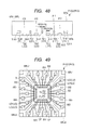
- FIG. 49 is a perspective plan view of a semiconductor device in a third modification.
- FIG. 50 is a perspective plan view of the semiconductor device in the third modification.
- FIG. 51 is a bottom view of the semiconductor device in the third modification.
- FIG. 52 is a side view of the semiconductor device in the third modification.
- FIG. 53 is a perspective plan view of a semiconductor device in a fourth modification
- FIG. 54 is a perspective plan view of the semiconductor device in the fourth modification.
- FIG. 55 is a bottom view of the semiconductor device in the fourth modification.
- FIG. 56 is a cross-sectional view of the semiconductor device in the fourth modification.
- FIG. 57 is a cross-sectional view of the semiconductor device in the fourth modification.
- FIG. 58 is a cross-sectional view of a semiconductor device in a fifth modification
- FIG. 59 is a cross-sectional view of the semiconductor device in the fifth modification.
- FIG. 60 is a side view of the semiconductor device in the fifth modification.
- FIG. 61 is a partially enlarged side view showing a part of FIG. 60 in enlarged relation.
- the embodiment will be described by being divided into a plurality of sections or embodiments. However, they are by no means irrelevant to each other unless particularly explicitly described otherwise, but are in relations such that one of the sections or embodiments is a modification, details, supplementary explanation, and so forth of part or the whole of the others. Also, in the following embodiments, when the number and the like (including the number, numerical value, amount, range, and the like) of elements are referred to, they are not limited to specific numbers unless particularly explicitly described otherwise or unless they are obviously limited to specific numbers in principle. The number and the like of the elements may be not less than or not more than specific numbers.
- the components thereof are not necessarily indispensable unless particularly explicitly described otherwise or unless the components are considered to be obviously indispensable in principle.
- the shapes, positional relationships, and the like of the components and the like are referred to in the following embodiment, the shapes and the like are assumed to include those substantially proximate or similar thereto and the like unless particularly explicitly described otherwise or unless it can be considered that they obviously do not in principle. The same shall apply in regard to the foregoing numerical value and range.
- hatching may be omitted even in a cross section for improved clarity of illustration, while even a plan view may be hatched for improved clarity of illustration.
- FIG. 1 is a top view of a semiconductor device PKG in the embodiment of the present invention.
- FIG. 2 is a bottom view (back-side view) of the semiconductor device PKG.
- FIGS. 3 to 5 are perspective plan views of the semiconductor device PKG.
- FIGS. 6 to 8 are cross-sectional views of the semiconductor device PKG.
- FIG. 9 is a side view of the semiconductor device PKG.
- FIG. 10 is a partially enlarged side view in which a part of FIG. 9 is enlarged.
- FIG. 11 is also a perspective plan view of the semiconductor device PKG.
- FIG. 3 shows a perspective plan view of the upper surface of the semiconductor device PKG when viewed through a sealing portion MR.
- FIG. 4 also shows a perspective plan view of the upper surface of the semiconductor device PKG when viewed also through wires BW in FIG. 3 .
- FIG. 5 shows a perspective plan view of the upper surface of the semiconductor device PKG when viewed also through a semiconductor chip CP in FIG. 4 .
- the cross section of the semiconductor device PKG at the position along the line A-A in each of FIGS. 1 and 3 corresponds to FIG. 6 .
- the cross section of the semiconductor device PKG at the position along the line B-B in each of FIGS. 1 and 3 corresponds to FIG. 7 .
- FIG. 9 shows a side view of a side surface MRc 1 of a sealing portion MR.
- a side view of a side surface MRc 2 of the sealing portion MR, a side view of a side surface MRc 3 of the sealing portion MR, and a side view of a side surface MRc 4 of the sealing portion MR are also similar to FIG. 9 .
- FIG. 10 shows an enlarged view of a region RG 1 enclosed by the dotted line in FIG. 9 .
- FIG. 11 shows the same perspective plan view as that shown in FIG. 5 , but the respective portions of leads LD 1 and LD 2 , a die pad DP, and suspension leads TL which have different thicknesses are hatched to be distinguishable from each other.
- the semiconductor device (semiconductor package) PKG in the present embodiment shown in each of FIGS. 1 to 11 is a semiconductor device in the form of a resin-sealed surface-mounted semiconductor package, which is a QFN (Quad Flat Non-Leaded package) type semiconductor device herein.
- QFN Quad Flat Non-Leaded package
- the semiconductor device PKG in the present embodiment shown in FIGS. 1 to 11 includes the semiconductor chip CP, the die pad (chip mounting portion or tab) DP over which the semiconductor chip CP is mounted, a plurality of leads LD formed of a conductor, the plurality of wires BW electrically connecting a plurality of pad electrodes PD of the semiconductor chip CP with the plurality of leads LD, and a sealing portion (resin sealing portion or sealed body) MR which seals the semiconductor chip CP, the die pad DP, the leads LD, and the wires BS.
- a sealing portion resin sealing portion or sealed body
- the sealing portion MR (resin-sealed body) is made of a resin material such as, e.g., a thermosetting resin material and can also contain a filler or the like.
- the sealing portion MR can be formed using an epoxy resin containing a filler or the like.
- an epoxy-based resin for the purpose of reducing a stress or the like, a biphenyl-based thermosetting resin to which, e.g., a phenol-based curing agent, silicone rubber, a filler, or the like is added may also be used as the material of the sealing portion MR.
- the sealing portion MR has an upper surface (top surface) MRa as one of the main surfaces thereof, a lower surface (back surface or bottom surface) MRb as the main surface opposite to the upper surface MRa, and the plurality of side surfaces MRc 1 , MRc 2 , MRc 3 , and MRc 4 crossing the upper and lower surfaces MRa and MRb. That is, the sealing portion MR has a thin-plate outer appearance defined by the upper and lower surfaces MRa and MRb and the plurality of side surfaces MTc 1 , MRc 2 , MRc 3 , and MRc 4 . The plurality of side surfaces MRc 1 , MRc 2 , MRc 3 , and MRc 4 are located between the upper and lower surfaces MRa and MRb.
- Each of the upper and lower surfaces MRa and MRb of the sealing portion MR has a rectangular (rectangle) shape. Accordingly, the sealing portion MR also has a rectangular two-dimensional shape and therefore has the four side surfaces MRc 1 , MRc 2 , MRc 3 , and MRc 4 .
- the side surfaces MRc 1 , MRc 2 , MRc 3 , and MRc 4 of the sealing portion MR are located opposite to each other, and the side surfaces MRc 2 and MRc 4 are located opposite to each other.
- the side surface MRc 1 and each of the side surfaces MRc 2 and MRc 4 cross each other, and the side surface MRc 3 and each of the side surfaces MRc 2 and MRc 4 cross each other.
- the side surfaces MRc 1 , MRc 2 , MRc 3 , and MRc 4 of the sealing portion MR are formed of cut surfaces (cut surfaces of a sealing portion MR 1 ) resulting from the cutting of the sealing portion MR 1 with a dicing blade BRD (rotary blade) described later. Accordingly, each of the side surfaces MRc 1 , MRc 2 , MRc 3 , and MRc 4 of the sealing portion MR as the cut surfaces is generally perpendicular to the lower and upper surfaces MRb and MRa of the sealing portion MR.
- the angle formed between the lower surface MRb of the sealing portion MR and each of the side surfaces MRc 1 , MRc 2 , MRc 3 , and MRc 4 thereof is about 90°
- the angle formed between the upper surface MRa of the sealing portion MR and each of the side surfaces MRc 1 , MRc 2 , MRc 3 , and MRc 4 thereof is also about 90°.
- an identification mark such as a product number can also be formed.
- the plurality of leads (lead portions) LD are formed of a conductor and preferably made of a metal material such as copper (Cu) or a copper alloy.
- the plurality of leads LD are sealed in the sealing portion MR.
- each of the leads LD has at least a portion thereof exposed from the lower surface MRb of the sealing portion MR.
- An end surface (end portion or cut surface) TM of each of the leads LD which is opposite to the end surface (end portion) thereof closer to the die pad DP is exposed from any of the side surfaces (MRc 1 , MRc 2 , MRc 3 , and MRc 4 ) of the sealing portion MR.
- each of the leads LD which is exposed from the lower surface MRb of the sealing portion MR functions as an external connection terminal portion (external terminal) of the semiconductor device PKG.
- Each of the leads LD scarcely protrudes from the side surface of the sealing portion MR.
- Each of the leads LD has the end surface (end portion) closer to the die pad DP and the end surface (end portion or cut surface) TM opposite thereto.
- the end surface (end portion) of each of the leads LD closer to the die pad DP is hereinafter referred to as the front end surface (front end portion) of the lead LD.
- the front end surface and the end surface TM of each of the leads LD are the end surfaces (end portions) located opposite to each other in the extending direction of the lead LD.
- the end surface TM of each of the leads LD is formed of the cut surface of the lead LD when the sealing portion MR 1 described later is cut with the dicing blade BRD (rotary blade) described later. Accordingly, the end surface TM of the lead LD can also be regarded as the cut surface of the lead LD. Consequently, the end surface TM of each of the leads LD scarcely protrudes from the side surface (MRc 1 , MRc 2 , MRc 3 , or MRc 4 ) of the sealing portion MR.
- the side surface (MRc 1 , MRc 2 , MRc 3 , or MRc 4 ) of the sealing portion MR and the end surfaces TM of the leads LD exposed thereat form substantially the same plane.
- the die pad DP is the chip mounting portion over which the semiconductor chip CP is mounted.
- the die pad DP is formed to have, e.g., a rectangular two-dimensional shape.
- the die pad DP has a side surface along the side surface MRc 1 of the sealing portion MR, a side surface along the side surface MRc 2 of the sealing portion MR, a side surface along the side surface MRc 3 of the sealing portion MR, and a side surface along the side surface MRc 4 of the sealing portion MR.
- the die pad DP is sealed in the sealing portion MR, but the lower surface of the die pad DP is exposed from the lower surface MRb of the sealing portion MR.
- FIGS. 2 and 6 to 8 shows the case where the lower surface of the die pad DP is exposed from the lower surface MRb of the sealing portion MR.
- the die pad DP is formed of a conductor and preferably made of a metal material such as copper (Cu) or a copper alloy. More preferably, the die pad DP and the plurality of leads LD each included in the semiconductor device PKG are formed of the same material. This facilitates the production of the lead frame in which the die pad DP and the plurality of leads LD are coupled to each other as well as the manufacturing of the semiconductor device PKG using the lead frame.
- a metal material such as copper (Cu) or a copper alloy.
- the plurality of leads LD included the semiconductor device PKG are disposed around the die pad DP in plan view. Accordingly, the plurality of leads LD included in the semiconductor device PKG include the plurality of leads LD disposed closer to the side surface MRc 1 of the sealing portion MR, the plurality of leads LD disposed closer to the side surface MRc 2 of the sealing portion MR, the plurality of leads LD disposed closer to the side surface MRc 3 of the sealing portion MR, and the plurality of leads LD disposed closer to the side surface MRc 4 of the sealing portion MR.
- the plurality of leads LD are disposed (arranged) along the side surface MRc 1 of the sealing portion MR and, between the die pad DP and the side surface MRc 2 of the sealing portion MR, the plurality of leads LD are disposed (arranged) along the side surface MRc 2 of the sealing portion MR.
- the plurality of leads LD are disposed (arranged) along the side surface MRc 3 of the sealing portion MR and, between the die pad DP and the side surface MRc 4 of the sealing portion MR, the plurality of leads LD are disposed (arranged) along the side surface MRc 4 of the sealing portion MR.
- the respective end surfaces TM of the plurality of leads LD disposed closer to the side surface MRc 1 of the sealing portion MR are exposed from the side surface MRc 1 of the sealing portion MR.
- the respective end surfaces TM of the plurality of leads LD disposed closer to the side surface MRc 2 of the sealing portion MR are exposed from the side surface MRc 2 of the sealing portion MR.
- the respective end surfaces TM of the plurality of leads LD disposed closer to the side surface MRc 3 of the sealing portion MR are exposed from the side surface MRc 3 of the sealing portion MR.
- the respective end surfaces TM of the plurality of leads LD disposed closer to the side surface MRc 4 of the sealing portion MR are exposed from the side surface MRc 4 of the sealing portion MR.
- each of the suspension leads TL is formed of the same material as that of the die pad DP to be integral with the die pad DP.
- the four corners of the outer edge of the die pad DP are formed integrally with the suspension leads LD.
- the suspension leads TL extend in the sealing portion having a rectangular two-dimensional shape toward the four corners of the sealing portion MR. In the case shown in FIGS. 3 to 5 , each of the suspension leads TL is branched to two portions in the vicinity of the corner portion of the sealing portion MR.
- the two front end surfaces (end surfaces TLM) resulting from the branching are exposed at the two side surfaces (side surfaces of the sealing portion MR) forming the corner portion.
- the end surfaces (exposed surfaces or cur surfaces) TLM of the suspension leads TL exposed from the side surfaces (MRc 1 , MRc 2 , MRc 3 , and MRc 4 ) of the sealing portion MR are formed of the cut surfaces of the suspension leads TL when the sealing portion MR 1 described later is cut with the dicing blade BRD (rotary blade) described later. Consequently, each of the suspension leads TL scarcely protrudes from the side surface of the sealing portion MR.
- the side surface (MRc 1 , MRc 2 , MRc 3 , or MRc 4 ) of the sealing portion MR and the end surfaces TLM of the suspension leads TL exposed thereat form substantially the same plane.
- the semiconductor chip CP is mounted with the top surface (upper surface) thereof facing upward and with the back surface (lower surface) thereof facing the die pad DP.
- the two-dimensional size (plane area) of the die pad DP is larger than the two-dimensional size (plane area) of the semiconductor chip CP.
- the semiconductor chip CP is included in the upper surface of the die pad DP.
- it may also be possible that the two-dimensional size of the die pad DP is smaller than the two-dimensional size of the semiconductor chip CP. In that case, in plan view, the outer peripheral portion of the semiconductor chip CP protrudes from the die pad DP.
- the main surface where the plurality of pad electrodes PD are formed is referred to as the top surface of the semiconductor chip CP and the main surface opposite to the top surface and facing the die pad DP is referred to as the back surface of the semiconductor chip CP.
- the semiconductor chip CP is manufactured by forming various semiconductor elements or semiconductor integrated circuits in the main surface of a semiconductor substrate (semiconductor wafer) made of, e.g., monocrystalline silicon or the like and then dividing the semiconductor substrate into individual semiconductor chips by dicing or the like.
- the two-dimensional shape of the semiconductor chip CP crossing the thickness thereof is a rectangle.
- the back surface of the semiconductor chip CP is bonded to the upper surface of the die pad DP via a bonding material (bonding material layer or an adhesion layer) BD to be fixed thereto.
- the semiconductor chip CP is sealed in the sealing portion MR and is not exposed from the sealing portion MR.
- the bonding material BD is a conductive material and where the bonding material BD is an insulating bonding material.
- the plurality of pad electrodes (pads or bonding pads) PD are formed over the top surface of the semiconductor chip CP.
- the plurality of pad electrodes PD of the semiconductor chip CP and the plurality of leads LD are electrically connected with each other via the plurality of wires (bonding wires) BW. That is, each of the wires BW has one end connected with the pad electrode PD of the semiconductor chip CP and the other end connected with the lead LD.
- the pad electrodes PD of the semiconductor chip CP and the leads LD are electrically connected with each other via the wires BW.
- the wires (bonding wires) BW are conductive connecting members. More specifically, the wires BW are conductive wires. Since the wires BW are made of metal, the wires BW can be regarded as metal wires (thin metal wires). As the wires BW, gold (Au) wires, copper (Cu) wires, aluminum (Al) wires, or the like can be used appropriately.
- the wires BW are sealed in the sealing portion MR and are not exposed from the sealing portion MR.
- the top surface of the semiconductor chip CP has a rectangular two-dimensional shape and has a side along the side surface MRc 1 of the sealing portion MR (side closer to the side surface MRc 1 ), a side along the side surface MRc 2 of the sealing portion MR (side closer to the side surface MRc 2 ), a side along the side surface MRc 3 of the sealing portion MR (side closer to the side surface MRc 3 ), and a side along the side surface MRc 4 of the sealing portion MR (side closer to the side surface MRc 4 ).
- the plurality of pad electrodes PD arranged along the side closer to the side surface MRc 1 over the top surface of the semiconductor chip CP are electrically connected with the plurality of leads LD disposed closer to the side surface MRc 1 of the sealing portion MR via the plurality of wires BW. Also, the plurality of pad electrodes PD arranged along the side closer to the side surface MRc 2 over the top surface of the semiconductor chip CP are electrically connected with the plurality of leads LD disposed closer to the side surface MRc 2 of the sealing portion MR via the plurality of wires BW.
- the plurality of pad electrodes PD arranged along the side closer to the side surface MRc 3 over the top surface of the semiconductor chip CP are electrically connected with the plurality of leads LD disposed closer to the side surface MRc 3 of the sealing portion MR via the plurality of wires BW.
- the plurality of pad electrodes PD arranged along the side closer to the side surface MRc 4 over the top surface of the semiconductor chip CP are electrically connected with the plurality of leads LD disposed closer to the side surface MRc 4 of the sealing portion MR via the plurality of wires BW.
- the plurality of leads LD included in the semiconductor device PKG are disposed around the die pad DP in plan view.
- the leads LD include the leads LD 1 and the leads LD 2 .
- the leads LD 1 and LD 2 are alternately disposed around the die pad DP in plan view. That is, along any of the side surfaces MRc 1 , MRc 2 , MRc 3 , and MRc 4 of the sealing portion MR, the leads LD 1 and LD 2 are alternately disposed.
- the lead LD next to each of the leads LD 1 is the lead LD 2
- the lead LD next to each of the leads LD 2 is the lead LD 1 .
- the leads LD 1 and LD 2 are next to each other.
- the leads LD 1 extend closer to the die pad DP than the leads LD 2 . That is, when a comparison is made between the leads LD 1 and LD 2 next to each other, the front end surface of each of the leads LD 1 is located closer to the die pad DP than the front end surface of each of the leads LD 2 . That is, when a comparison is made between the leads LD 1 and LD 2 next to each other, the distance (space) between the front end surface of the lead LD 1 and the die pad DP is shorter than the distance (space) between the front end surface of the lead LD 2 and the die pad DP.
- Each of the leads LD 1 integrally has a thicker portion (larger thickness portion) LD 1 a having a larger thickness and a thinner portion (smaller thickness portion) LD 1 b having a smaller thickness (see FIG. 6 ).
- each of the leads LD 2 integrally has a thicker portion (larger thickness portion) LD 2 a having a larger thickness and a thinner portion (smaller thickness portion) LD 2 b having a smaller thickness (see FIG. 7 ).
- a thickness T 1 b of the thinner portion LD 1 b is smaller than a thickness T 1 a of the thicker portion LD 1 a (i.e., T 1 b ⁇ T 1 a is satisfied).
- a thickness T 2 b of the thinner portion LD 2 b is smaller than a thickness T 2 a of the thicker portion LD 2 a (i.e., T 2 b ⁇ T 2 a is satisfied).
- the lead LD 1 integrally has the thicker portion LD 1 a (first thicker portion) and the thinner portion LD 1 b (first thinner portion) thinner than the thicker portion LD 1 a which are next to each other in the extending direction of the lead LD 1 .
- the thicker portion LD 1 a is located closer to the die pad DP than the thinner portion LD 1 b .
- the lead LD 2 (second lead) integrally has the thicker portion LD 2 a (second thicker portion) and the thinner portion LD 2 b (second thinner portion) thinner than the thicker portion LD 2 a which are next to each other in the extending direction of the lead LD 2 .
- the thicker portion LD 2 a is located closer to the die pad DP than the thinner portion LD 2 b.
- the leads LD 1 and LD 2 , the die pad DP, and the suspension leads TL are hatched to allow the respective thicknesses thereof to be recognized.
- the regions hatched with dots are thicker regions and therefore the die pad DP, the thicker portions LD 1 a of the leads LD 1 , and the thicker portions LD 2 a of the leads LD 2 are hatched with dots.
- the regions hatched with oblique lines are thinner regions and therefore the thinner portions LD 1 b of the leads LD 1 , the thinner portions LD 2 b of the leads LD 2 , and the suspension leads TL are hatched with oblique lines.
- the oblique lines hatching the thinner portions LD 1 b of the leads LD 1 and the oblique lines hatching the thinner portions LD 2 b of the leads LD 2 are provided in different orientations. This is because the thickness of each of the thinner portions LD 1 b of the leads LD 1 is reduced by half etching performed on the lower surface thereof, while the thickness of each of the thinner portions LD 2 b of the leads LD 2 is reduced by half etching performed on the upper surface thereof.
- the oblique lines hatching the thinner portions LD 1 b of the leads LD 1 and the oblique lines hatching the suspension leads TL are provided in the same orientation.
- width W 1 b of the thinner portion LD 1 b of each of the leads LD 1 and the width W 1 a of the thicker portion LD 1 a of the lead LD 1 correspond to widths (dimensions) in directions parallel with the lower surface MRb of the sealing portion MR and generally perpendicular to the extending direction of the lead LD 1 .
- width W 2 b of the thinner portion LD 2 b of each of the leads LD 2 and the width W 2 a of the thicker portion LD 2 a of the lead LD 2 correspond to widths (dimensions) in directions parallel with the lower surface MRb of the sealing portion MR and generally perpendicular to the extending direction of the lead LD 2 .
- the lateral dimension W 3 of the end surface TM 1 of the lead LD 1 corresponds to the dimension (length) of the end surface TM 1 in a direction parallel with the lower surface MRb of the sealing portion MR 1 and accordingly corresponds to the dimension (length) of the end surface TM 1 in a direction parallel with the lower surface MRb of the sealing portion MR 1 and parallel with the end surface TM 1 .
- the lateral dimension W 4 of the end surface TM 2 of the lead LD 2 corresponds to the dimension (length) of the end surface TM 2 in a direction parallel with the lower surface MRb of the sealing portion MR 1 and accordingly corresponds to the dimension (length) of the end surface TM 2 in a direction parallel with the lower surface MRb of the sealing portion MR 1 and parallel with the end surface TM 2 .
- the end surface TM 1 of the lead LD 1 is formed of the cut surface of the thinner portion LD 1 b of the lead LD 1
- the thinner portion LD 1 b of each of the leads LD 1 is formed by performing half etching on the lower surface of the portion of the lead LD 1 which serves as the thinner portion LD 1 b and thus reducing the thickness thereof when the lead frame used to manufacture the semiconductor device PKG is produced. That is, in the lead LD 1 , the thinner portion LD 1 b corresponds to the region subjected to the half etching performed on the lower surface thereof and thus having a reduced thickness and the thicker portion LD 1 a corresponds to the region not subjected to the half etching.
- the thinner portion LD 2 b of each of the leads LD 2 is formed by performing half etching on the upper surface of the portion of the lead LD 2 which serves as the thinner portion LD 2 b and thus reducing the thickness thereof when the lead frame used to manufacture the semiconductor device PKG is produced. That is, in the lead LD 2 , the thinner portion LD 2 b corresponds to the region subjected to the half etching performed on the upper surface thereof and thus having a reduced thickness and the thicker portion LD 2 a corresponds to the region not subjected to the half etching.
- the respective upper surfaces of the thinner portion LD 1 b and the thicker portion LD 1 a are at the same height position so that no step is formed between the respective upper surfaces of the thinner portion LD 1 b and the thicker portion LD 1 a . That is, in the lead LD 1 , the respective upper surfaces of the thinner portion LD 1 b and the thicker portion LD 1 a are located on the same plane. However, in the lead LD 1 , the respective lower surfaces of the thinner portion LD 1 b and the thicker portion LD 1 a are at different height positions.
- the lower surface of the thinner portion LD 1 b is at a position higher than that of the lower surface of the thicker portion LD 1 a so that a step is formed between the respective lower surfaces of the thinner portion LD 1 b and the thicker portion LD 1 a (see FIG. 6 ).
- the respective lower surfaces of the thinner portion LD 2 b and the thicker portion LD 2 a are at the same height position so that no step is formed between the respective lower surfaces of the thinner portion LD 2 b and the thicker portion LD 2 a . That is, in the lead LD 2 , the respective lower surfaces of the thinner portion LD 2 b and the thicker portion LD 2 a are located on the same plane. However, in the lead LD 2 , the respective upper surfaces of the thinner portion LD 2 b and the thicker portion LD 2 a are at different height positions.
- the upper surface of the thinner portion LD 2 b is at a position lower than that of the upper surface of the thicker portion LD 2 a so that a step is formed between the respective upper surfaces of the thinner portion LD 2 b and the thicker portion LD 2 a (see FIG. 7 ).
- the thicker portion LD 1 a and the thinner portion LD 1 b are next to each other in the extending direction of the lead LD 1 .
- the thicker portion LD 1 a is located closer to the die pad DP, while the thinner portion LD 1 b is located closer to the side surface of the sealing portion MR.
- the thicker portion LD 2 a and the thinner portion LD 2 b are next to each other in the extending direction of the lead LD 2 .
- the thicker portion LD 2 a is located closer to the die pad DP, while the thinner portion LD 2 b is located closer to the side surface of the sealing portion MR.
- each of the leads LD 1 the lower surface of the thicker portion LD 1 a is exposed from the lower surface MR of the sealing portion MR, while the lower surface of the thinner portion LD 1 b is covered with the sealing portion MR and is not exposed from the lower surface MRb of the sealing portion MR.
- the respective lower surfaces of the thicker portion LD 2 a and the thinner portion LD 2 b are exposed from the lower surface MRb of the sealing portion MR. Consequently, each of the leads LD 2 has the entire lower surface thereof exposed from the lower surface MRb of the sealing portion MR.
- the lower surface of the semiconductor device PKG corresponding to the lower surface MRb of the sealing portion MR serves as the mounting surface of the semiconductor device PKG.
- the respective lower surfaces of the thicker portions LD 1 a of the leads LD 1 and the entire lower surfaces of the leads LD 2 are exposed from the lower surface MRb of the sealing portion MR to function as the external terminals of the semiconductor device PKG. It is assumed herein that the exposed surfaces of the leads LD 1 at the lower surface MRb of the sealing portion MR are referred to as the lower exposed surfaces of the leads LD 1 , and the exposed surfaces of the leads LD 2 at the lower surface MRb of the sealing portion MR are referred to as the lower exposed surfaces of the leads LD 2 .
- the lower exposed surfaces of the leads LD 1 are formed of the lower surfaces of the thicker portions LD 1 a of the leads LD 1
- the lower exposed surfaces of the leads LD 2 are formed of the entire lower surfaces of the leads LD 2
- the lower exposed surface of each of the leads LD 1 and LD 2 has a rectangular two-dimensional shape.
- the two-dimensional size (plane area) of the thicker portion LD 1 a of each of the leads LD 1 is substantially equal to the two-dimensional size (plane area) of the thicker portion LD 2 a of each of the leads LD 2 .
- the area of the lower exposed surfaces of the leads LD 2 is larger than the area of the lower exposed surfaces of the leads LD 1 .
- the distance between the thicker portion LD 1 a of each of the leads LD 1 and the die pad DP is smaller than the distance between the thicker portion LD 2 a of each of the leads LD 2 next to the lead LD 1 and the die pad DP. Accordingly, the thicker portion LD 1 a of the lead LD 1 is located closer to the die pad DP than the thicker portion LD 2 a of the lead LD 2 .
- the distance between the lower exposed surface of the lead LD 1 and the die pad DP is smaller than the distance between the lower exposed surface of the lead LD 2 next to the lead LD 1 and the die pad DP. Accordingly, the lower exposed surface of the lead LD 1 is located closer to the die pad DP than the lower exposed surface of the lead LD 2 .
- the lower exposed surfaces of the leads LD 2 are located in the peripheral region (outer peripheral portion) of the lower surface MRb of the sealing portion MR and disposed herein at positions adjoining the lateral sides of the lower surface MRb of the sealing portion MR.
- the lateral sides of the lower surface MRb of the sealing portion MR correspond herein to the sides of the lower surface MRb of the sealing portion MR which form the outermost periphery of the lower surface MRb of the sealing portion MR.
- the lateral sides of the lower surface MRb of the sealing portion MR are also next to the side surfaces of the sealing portion MR.
- the lower exposed surfaces of the leads LD 1 are disposed at positions inward of the lower exposed surfaces of the leads LD 2 .
- the lower exposed surface of each of the leads LD 1 is disposed herein at a position away from the lateral side of the lower surface MRb of the sealing portion MR by a distance L 1 (L 1 >0) (see FIG. 2 ).
- the leads LD 1 and LD 2 are alternately disposed (arranged) around the die pad DP.
- the respective lower exposed surfaces of the leads LD 1 and LD 2 functioning as the external terminals of the semiconductor device PKG are disposed in two rows in a staggered configuration (staggered arrangement) along the lateral sides (outer periphery) of the lower surface MRb of the sealing portion MR in the regions in the vicinity of the peripheral portion thereof.
- the respective end surfaces TM of the leads LD 1 and LD 2 are exposed from the side surfaces MRc 1 , MRc 2 , MRc 3 , and MRc 4 of the sealing portion MR. It is assumed herein that the end surface TM of each of the leads LD 1 is referred to as the end surface TM 1 using a reference numeral TM 1 , and the end surface TM of each of the leads LD 2 is referred to as the end surface TM 2 using a reference numeral TM 2 .
- the end surface TM 1 of each of the leads LD 1 is next to the thinner portion LD 1 b of the lead LD 1 and serves as the end surface (cut surface) of the thinner portion LD 1 b of the lead LD 1 .
- the end surface TM 2 of each of the leads LD 2 is next to the thinner portion LD 2 b of the lead LD 2 and serves as the end surface (cut surface) of the thinner portion LD 2 b of the lead LD 2 . That is, the end surface TM 1 is formed of the thinner portion LD 1 b of the lead LD 1 , while the end surface TM 2 is formed of the thinner portion LD 2 b of the lead LD 2 .
- the end surface TM 1 is the cut surface of the thinner portion LD 1 b resulting from cutting with the dicing blade BRD (rotary blade) described later
- the end surface TM 2 is the cut surface of the thinner portion LD 2 b resulting from cutting with the dicing blade BRD (rotary blade) described later.
- the end surfaces TM 1 of the leads LD 1 and the end surfaces TM 2 of the leads LD 2 are alternately arranged.
- the height position of the end surface TM 1 of each of the leads LD 1 is different from the height position of the end surface TM 2 of each of the leads LD 2 .
- the height position of the end surface TM 1 of the lead LD 1 is higher than the height position of the end surface TM 2 of the lead LD 2 .
- the height position of the end surface TM 2 of the lead LD 2 is lower than the height position of the end surface TM 1 of the lead LD 1 .
- the “height” or “height position” is based on the lower surface MRb of the sealing portion MR. It is assumed that the side of the sealing portion MR closer to the upper surface MRa thereof (i.e., the side of the sealing portion MR far away from the lower surface MRb thereof) is assumed to be a higher side and the side of the sealing portion MR far away from the upper surface MR 1 thereof (i.e., the side of the sealing portion MR closer to the lower surface MRb thereof) is assumed to be a lower side.
- the “height direction” is the same as the “thickness direction of the sealing portion MR” and corresponds to a direction generally perpendicular to the lower surface MRb or upper surface MRa of the sealing portion MR. Accordingly, the dimension H 1 of the end surface TM 1 corresponds to the dimension of the end surface TM 1 in the thickness direction of the sealing portion MR, and the dimension H 2 of the end surface TM 2 corresponds to the dimension of the end surface TM 2 in the thickness direction of the sealing portion MR.
- the end surface TM 1 of each of the leads LD 1 has a lower side KH 1 and an upper side JH 1
- the end surface TM 2 of each of the leads LD 2 has a lower side KH 2 and an upper side JH 2 (see FIGS. 9 and 10 ). That is, the end surface TM 1 (first end surface) of the lead LD 1 (first lead) has the upper side JH 1 (first upper side) closer to the upper surface MRa of the sealing portion MR and the lower side KH 1 (first lower side) far away from the upper surface MRa of the sealing portion MR.
- the end surface TM 2 (second end surface) of the lead LD 2 (second lead) has the upper side JH 2 (second upper side) closer to the upper surface MRa of the sealing portion MR and the lower side KH 2 (second lower side) far away from the upper surface MRa of the sealing portion MR.
- the lower side KH 1 of the end surface TM 1 of each of the leads LD 1 corresponds to the lower side (closer to the lower surface MRb of the sealing portion MR) of a two-dimensional shape (which is more specifically a quadrilateral shape) forming the end surface TM 1 of the lead LD 1
- the upper side JH 1 of the end surface TM 1 of the lead LD 1 corresponds to the upper side (closer to the upper surface MRa of the sealing portion MR) of the two-dimensional shape (which is more specifically the quadrilateral shape) forming the end surface TM 1 of the lead LD 1 .
- the lower side KH 2 of the end surface TM 2 of each of the leads LD 2 corresponds to the lower side (closer to the lower surface MRb of the sealing portion MR) of a two-dimensional shape (which is more specifically a quadrilateral shape) forming the end surface TM 2 of the lead LD 2
- the upper side JH 2 of the end surface TM 2 of the lead LD 2 corresponds to the upper side (closer to the upper surface MRa of the sealing portion MR) of the two-dimensional shape (which is more specifically the quadrilateral shape) forming the end surface TM 2 of the lead LD 2 .
- the upper side JH 2 of the end surface TM 2 of the lead LD 2 is at a position lower than that of the lower side KH 1 of the end surface TM 1 of the lead LD 1 . That is, when a comparison is made between the lower side KH 1 of the end surface TM 1 of the lead LD 1 and the upper side JH 2 of the end surface TM 2 of the lead LD 2 , the lower side KH 1 of the end surface TM 1 of the lead LD 1 is at a position closer to the upper surface MRa of the sealing portion MR than the upper side JH 2 of the end surface TM 2 of the lead LD 2 , and the upper side JH 2 of the end surface TM 2 of the lead LD 2 is at a position closer to the lower surface MRb of the sealing portion MR than the lower side KH 1 of the end surface TM 1 of the lead LD 1 .
- a distance (distance in the thickness direction of the sealing portion MR) L 2 between the lower side KH 1 of the end surface TM 1 of the lead LD 1 and the upper surface MRa (i.e., side of the upper surface MRa shown in FIG. 9 ) of the sealing portion MR is smaller than a distance (distance in the thickness direction of the sealing portion MR) L 3 between the upper side JH 2 of the end surface TM 2 of the lead LD 2 and the upper surface MRa (i.e., side of the upper surface MRa shown in FIG. 9 ) of the sealing portion MR (i.e., L 2 ⁇ L 3 is satisfied).
- each of the distances L 2 and L 3 is a distance in the thickness direction of the sealing portion MR and shown in FIG. 9 .
- the thickness of the thinner portion LD 1 b of each of the leads LD 1 is reduced by half etching performed on the lower surface thereof, while the thickness of the thinner portion LD 2 b of each of the leads LD 2 is reduced by half etching performed on the upper surface thereof.
- the end surface TM 1 as the cut surface of the thinner portion LD 1 b of the lead LD 1 and the end surface TM 2 as the cut surface of the thinner portion LD 2 b of the lead LD 2 are exposed from the side surfaces MRc 1 , MRc 2 , MRc 3 , and MRc 4 of the sealing portion MR.
- the height position of the end surface TM 1 of the lead LD 1 is higher than the height position of the end surface TM 2 of the lead LD 2 .
- the lower side KH 1 of the end surface TM 1 of the lead LD 1 is at a position higher than that of the upper side JH 2 of the end surface TM 2 of the lead LD 2 .
- the lower side KH 1 of the end surface TM 1 is at a position higher than that of the upper side JH 2 of the end surface TM 2 , the following also holds true. That is, even when one of the end surface TM 1 of the lead LD 1 and the end surface TM 2 of the lead KD 2 which are next to each other at the side surface MRc 1 of the sealing portion MR is virtually moved in a lateral direction (direction parallel with the lower surface MRb and the side surface MRc 1 of the sealing portion MR), the virtually moved one of the end surfaces TM 1 and TM 2 does not overlap the other of the end surfaces TM 1 and TM 2 . The same applies also to the side surfaces MRc 2 , MRc 3 , and MRc 4 of the sealing portion MR.
- the lower surfaces of the suspension leads TL are not exposed but, from the side surfaces MRc 1 , MRc 2 , MRc 3 , and MRc 4 of the sealing portion MR, the end surfaces TLM of the suspension leads TL are exposed.
- the dimension of the end surface TLM of each of the suspension leads TL in the height direction is substantially equal to the thickness T 3 of the suspension lead TL.
- the height position of the end surface TLM of each of the suspension leads TL is substantially equal to the height position of the end surface TM 1 of each of the leads LD 1 and is accordingly higher than the height position of the end surface TM 2 of each of the leads LD 2 .
- the end surface TLM of the suspension lead TL is at a position closer to the upper surface MRa of the sealing portion MR (position far away from the lower surface MRb of the sealing portion MR) than the end surface TM 2 of the lead LD 2 .
- the end surface TM of the lead LD located next to the end surfaces TLM of each of the suspension leads TL is not the end surface TM 1 of the lead LD 1 , but the end surface TM 2 of the lead LD 2 .
- the end surface TLM of the suspension lead TL has an upper side TLJH closer to the upper surface MRa of the sealing portion MR and the lower side TLKH far away from the upper surface MRa of the sealing portion MR.
- the lower side TLKH of the end surface TLM of the suspension lead TL corresponds to a lower side (closer to the lower surface MRb of the sealing portion MR) of a quadrilateral shape forming the end surface TLM of the suspension lead TL.
- the lower side TLKH of the end surface TLM of the suspension lead TL is at a position higher than that of the upper side JH 2 of the end surface TM 2 of the lead LD 2 .
- the upper side JH 2 of the end surface TM 2 of the lead LD 2 is at a position lower than that of the lower side TLKH of the end surface TLM of the suspension lead TL.
- the lower side TLKH of the end surface TLM of the suspension lead TL is at a position closer to the upper surface MRa of the sealing portion MR (i.e., position far away from the lower surface MRb of the sealing portion MR) than the upper side JH 2 of the end surface TM 2 of the lead LD 2 .
- the distance (distance in the thickness direction of the sealing portion MR) between the lower side TLKH of the end surface TLM of the suspension lead TL and the upper surface MRa (i.e., side of the upper surface MRa shown in FIG. 9 ) of the sealing portion MR is smaller than the distance (distance in the thickness direction of the sealing portion MR) between the upper side JH 2 of the end surface TM 2 of the lead LD 2 and the upper surface MRa (i.e., side of the upper surface MRa shown in FIG. 9 ) of the sealing portion MR.
- plating layers (plating films) PL are formed (see FIGS. 6 to 8 ).
- Each of the plating layers PL is made of a metal layer formed by a plating method and is, e.g., a solder plating layer.
- the plating layers PL formed over the respective lower exposed surfaces of the leads LD 1 and LD 2 can improve the reliability of the electrical connection between the terminals or conductor pattern of a mounting substrate and the terminals (lower exposed surfaces of the leads LD 1 and LD 2 ) of the semiconductor device PKG when the semiconductor device PKG is mounted over the mounting substrate. Note that, in FIG. 2 , the plating layers PL are not shown, but the plating layers PL are formed over the respective lower exposed surfaces of the leads LD 1 and LD 2 and the lower surface of the die pad DP which are shown in FIG. 2 .
- the plating layers PL are not formed over the end surfaces TM 1 and TM 2 of the leads LD 1 and LD 2 and over the end surfaces TLM of the suspension leads TL.
- a semiconductor package of a type other than the QFN type e.g., a semiconductor package of a SON (Small Outline Non-leaded package) type to the semiconductor device PKG.
- the case where not only the lower surface of the thicker portion LD 2 a of each of the leads LD 2 , but also the lower surface of the thinner portion LD 2 b of the lead LD 2 is exposed from the lower surface MRb of the sealing portion MR as in the present embodiment is preferred to the case where the lower surface of the thinner portion LD 2 b of the lead LD 2 is not exposed from the lower surface MRb of the sealing portion MR.
- the area of the lower exposed surface of the lead LD 2 can be increased.
- the semiconductor device PKG when the semiconductor device PKG is mounted over the mounting substrate or the like, it is possible to further improve the bonding strength between the lead LD 2 of the semiconductor device PKG and the terminal of the mounting substrate. Therefore, it is possible to further improve the mounting reliability of the semiconductor device PKG.
- FIG. 12 is a process flow chart showing the manufacturing process of the semiconductor device PKG in the present embodiment.
- FIGS. 13 to 33 is a plan view or a cross-sectional view showing the manufacturing process of the semiconductor device PKG in the present embodiment.
- FIGS. 13, 17, 20, 23, 28, and 31 are plan views (top views)
- FIGS. 14 to 16, 18, 19, 21, 22, 24 to 27, 29, 30, 32, and 33 are cross-sectional views.
- FIGS. 14, 18, 21, 24, 26, 29, and 32 correspond to a cross-sectional view (cross-sectional view corresponding to FIG. 6 described above) at a position corresponding to the line D-D in FIG.
- FIGS. 15, 19, 22, 25, 27, 30, and 33 correspond to a cross-sectional view (cross-sectional view corresponding to FIG. 7 described above) at a position corresponding to the line E-E in FIG. 13 .
- FIG. 16 corresponds to a cross-sectional view at a position corresponding to the line F-F in FIG. 13 .
- a lead frame LF for manufacturing the semiconductor device PKG is provided (prepared) (Step S 1 in FIG. 12 ).
- the lead frame LF has a plurality of semiconductor device regions (device regions) PE.
- each of the semiconductor device regions PE corresponds to a region from which the one semiconductor device PKG is acquired (manufactured). That is, in the lead frame LF, the plurality of (multiple) semiconductor device regions PE are arranged in an array (in rows and columns).
- FIG. 13 shows a plan view of two of the plurality of semiconductor device regions PE. In FIG. 13 , the regions enclosed by the dotted lines correspond to the semiconductor device regions PE.
- FIGS. 14 and 15 also shows a cross-sectional view of the two semiconductor device regions PE. The regions between the adjacent semiconductor device regions PE correspond to dicing lines (regions to be cut) in Step S 6 described later.
- each of the semiconductor device regions PE of the lead frame LF the die pad DP and the plurality of leads LD (LD 1 and LD 2 ) for manufacturing the semiconductor device PKG are disposed.
- a dam bar (tie bar) DB is disposed between the adjacent semiconductor device regions PE.
- the dam bar DB extends along the sides of the semiconductor device regions PE on both sides thereof between the adjacent semiconductor device regions PE. Accordingly, in plan view, each of the semiconductor device regions PE is circumferentially surrounded by the dam bar DB.
- the dam bar DB extends in a grid-like pattern and, in each of the grids, the semiconductor device region PE is located. Since the dam bar DB is disposed in the region between the adjacent semiconductor device regions PE, the dam bar DB is cut and removed in a dicing step in Step S 6 described later.
- the lead frame LF is produced by etching.
- the leads of the lead frame can be formed more easily by etching than by press working.
- the lead frame LF by producing the lead frame LF by etching, the lead frame LF including the leads LD 1 each integrally having the thicker portion LD 1 a and the thinner portion LD 1 b and the leads LD 2 each integrally having the thicker portion LD 2 a and the thinner portion LD 2 b can reliably be produced.
- Each of the semiconductor device regions PE of the lead frame LF has the die pad DP as the chip mounting portion, the plurality of suspension leads TL supporting the die pad DP, and the plurality of leads LD.
- the die pad DP is disposed substantially at the center thereof and, around the die pad DP, the plurality of leads LD (LD 1 and LD 2 ) are disposed.
- the plurality of leads LD disposed around the die pad DP include the leads LD 1 and LD 2 which are alternately disposed.
- the plurality of leads LD (LD 1 and LD 2 ) disposed around the die pad DP are coupled to and held by the dam bar DB surrounding the semiconductor device region PR.
- the die pad DP is also coupled to and held by the dam bar DB surrounding the semiconductor device region PE via the plurality of suspension leads TL.
- the dam bar DB can also be regarded as a coupling portion for coupling the plurality of leads LD to each other.
- the plurality of leads (LD 1 and LD 2 ) in each of the semiconductor device regions PE are integrally connected with (coupled to) the dam bar DB. That is, an end portion of each of the leads LD (LD 1 and LD 2 ) which is opposite to the end portion (front end portion) thereof closer to the die pad DP is connected integrally with the dam bar DP.
- the die pad DP in each of the semiconductor device regions PE is integrally connected with (coupled to) the dam bar DB via the suspension leads TL. That is, an end portion of each of the suspension leads TL which is opposite to the end portion thereof connected with the die pad DP is integrally connected with the dam bar DB.
- the dam bar DB can function to couple the plurality of leads LD (LD 1 and LD 2 ) disposed closer to the dam bar DB in the semiconductor device regions PE on both sides of the dam bar DB to each other and hold the leads LD.
- the outermost periphery of the lead frame LF is made of a framework (not shown). In the outermost one of the plurality of semiconductor device regions PE arranged in an array, the leads LD next to the framework are integrally connected with (coupled to) the framework.
- the lead frame LF integrally has the leads LD (LD 1 and LD 2 ), the die pad DP, the suspension leads TL, the dam bar DB, and the framework.
- Each of the leads LD 1 integrally has the thicker portion LD 1 a and the thinner portion LD 1 b which are next to each other in the extending direction of the lead LD 1 .
- Each of the leads LD 2 integrally has the thicker portion LD 2 a and the thinner portion LD 2 b which are next to each other in the extending direction of the lead LD 2 .
- the thicker portion LD 1 a is located closer to the die pad DP and the thinner portion LD 1 b extends toward the dam bar DB to be integrally connected with the dam bar DB.
- each of the leads LD 2 the thicker portion LD 2 a is located closer to the die pad DP and the thinner portion LD 2 b extends toward the dam bar DB to be integrally connected with the dam bar DB.
- An end portion of each of the suspension leads TL which is opposite to the end portion thereof connected with the die pad DP extends toward the dam bar DB to be integrally connected with the dam bar DB.
- the dam bar DB integrally has portions DB 1 connected with the thinner portions LD 1 b of the leads LD 1 , portions DB 2 connected with the thinner portions LD 2 b of the leads LD 2 , portions DB 3 connected with the suspension leads TL, and the portions located therebetween.
- each of the portions (middle portions) between these portions DB 1 , DB 2 , and DB 3 has a thickness (T 4 d ) which is larger than the respective thicknesses (T 4 a , T 4 b , and T 4 c ) of these portions DP 1 , DB 2 , and DB 3 . That is, the thickness (T 4 d ) of each of the middle portions of the dam bar DB is larger than the respective thicknesses (T 4 a , T 4 b , and T 4 c ) of the portions DB 1 , DB 2 , and DB 3 mentioned above.
- T 4 d >T 4 a , T 4 d >T 4 b , and T 4 d >T 4 c are satisfied.
- the middle portions of the dam bar DB mentioned herein correspond to the portions of the dam bar DB which are other than the portions DB 1 , DB 2 , and DB 3 of the dam bar DB and include the portions of the dam bar DB which are located between the portions DB 1 and DB 2 and the portions of the dam bar DB which are located between the portions DB 2 and DB 3 .
- the thickness (T 4 a ) of each of the portions DB 1 of the dam bar DB which are connected with the leads LD 1 and the thickness (T 4 b ) of each of the portions DB 2 of the dam bar DB which are connected with the leads LD 2 are smaller than the thickness (T 4 d ) of each of the portions of the dam bar DB which are located between the portions DB 1 and DB 2 (T 4 d >T 4 a and T 4 d >T 4 b ).
- the thinner portions LD 1 b of the leads LD 1 and the portions DB 1 of the dam bar DB which are connected with the thinner portions LD 1 b of the leads LD 1 have thicknesses reduced by half etching performed on the lower surfaces thereof.
- the thinner portions LD 2 b of the leads LD 2 and the portions DB 2 of the dam bar DB which are connected with the thinner portions LD 2 b of the leads LD 2 have thicknesses reduced by half etching performed on the upper surfaces thereof.
- the suspension leads TL and the portions DB 3 of the dam bar DB which are connected with the suspension leads TL have thicknesses reduced by half etching performed on the lower surfaces thereof.
- the portions of the dam bar DB (middle portions of the dam bar DB) which are located between the portions DB 1 , DB 2 , and DB 3 correspond to regions not subjected to half etching.
- the dam bar DB may also have equal thicknesses.
- the foregoing portions DB 1 , DB 2 , and DB 3 of the dam bar DB and the portions (middle portions) of the dam bar DB which are located therebetween have substantially equal thicknesses which are substantially equal to the respective thicknesses of the thicker portions LD 1 a and LD 2 a of the leads LD 1 and LD 2 . That is, in this case, the thinner portions LD 1 b and LD 2 b and the suspension leads TL which are thinner than the dam bar DB are integrally connected with the dam bar DB having an overall thickness which is substantially equal to those of the thicker portions LD 1 a and LD 2 a .
- the dam bar DB is cut in the dicing step in Step S 6 described later to be removed and, as the volume of the dam bar DB is smaller, the dicing step is more easily performed.
- the portions DB 1 connected with the thinner portions LD 1 b of the leads LD 1 preferably have thicknesses equal to those of the thinner portions LD 1 b .
- the portions DB 2 connected with the thinner portions LD 2 b of the leads LD 2 preferably have thicknesses equal to those of the thinner portions LD 2 b .
- the portions DB 3 connected with the suspension leads TL preferably have thicknesses equal to those of the suspension leads TL. This can reduce the volume of the dam bar DB and therefore facilitates the dicing step in Step S 6 . This can also elongate the use lifetime of the dicing blade BRD described later.
- the thicknesses of the portions of the dam bar DB are set larger than those of the portions DB 1 , DB 2 , and DB 3 and are preferably set substantially equal to those of the thicker portions LD 1 a and LD 2 a of the leads LD 1 and LD 2 . This can integrally connect the portions DB 1 , DB 2 , and DB 3 with each other and assure the strength of the dam bar DB.
- a die bonding step is performed to mount the semiconductor chip CP over the upper surface of the die pad DP via the bonding material BD in each of the semiconductor device regions PE of the lead frame LF and bond (fix) the semiconductor chip CP thereto (Step S 2 in FIG. 12 ).
- the die bonding step in Step S 2 includes the steps of, e.g., applying the bonding material BD onto the upper surface of the die pad DP, then mounting the semiconductor chip CP over the upper surface of the die pad DP, and then solidifying the bonding material BD.
- a wire bonding step is performed to electrically connect the plurality of pad electrodes PD of the semiconductor chip CP in each of the semiconductor device regions PE with the plurality of leads LD (LD 1 and LD 2 ) in the semiconductor device region PE via the plurality of wires BW (Step S 3 in FIG. 12 ).
- resin sealing is performed using a molding step to form the sealing portion (batch molding portion) MR 1 as a resin sealing portion (resin-sealed body) to seal the die pad DP, the semiconductor chip CP, the wires BW, the leads LD (LD 1 and LD 2 ), and the suspension leads TL in each of the plurality of semiconductor device regions PE with the sealing portion MR 1 (Step S 4 in FIG. 12 ).
- the molding step include a transfer molding step.
- Step S 4 batch molding is performed to batch-mold the plurality of semiconductor device regions PE of the lead frame LF with the sealing portion MR 1 . That is, the sealing portion MR 1 is formed so as to cover the plurality of whole semiconductor device regions PE of the lead frame LF. As a result, the sealing portion MR 1 is formed not only over the semiconductor device regions PE but also between the adjacent semiconductor device regions PE, and the dam bar DB is also sealed with the sealing portion MR 1 . That is, over the plurality of whole semiconductor device regions PE of the lead frame LF, the semiconductor chips CP, the wires BW, the die pads, the leads LD, the suspension leads TL, and the dam bar DB are sealed with the sealing portion MR 1 .
- the sealing portion MR 1 is made of, e.g., a resin material such as a thermosetting resin material or the like and can also contain a filler or the like.
- the sealing portion MR 1 can be formed using an epoxy resin containing a filler or the like.
- the sealing portion MR 1 can be formed by disposing the lead frame LF in a mold such that the plurality of semiconductor device regions PE of the lead frame LF are located in the cavity of the mold, then injecting a sealing resin material into the cavity of the mold, and curing the sealing resin material by heating.
- the sealing portion MR 1 has an upper surface MR 1 a and a lower surface MR 1 b which are located opposite to each other.
- each of the leads LD in each of the semiconductor device regions PE has at least a portion exposed from the lower surface MR 1 b of the sealing portion MR 1 .
- the lower surface of the thicker portion LD 1 a is exposed from the lower surface MR 1 of the sealing portion MR 1
- the lower surface of the thinner portion LD 1 b is covered with the sealing portion MR 1 and is not exposed from the lower surface MR 1 b of the sealing portion MR 1 .
- each of the leads LD 2 has the entire lower surface thereof exposed from the lower surface MR 1 b of the sealing portion MR 1 .
- the plating layers PL are formed over the lower exposed surfaces of the leads LD 1 and LD 2 exposed from the lower surface MR 1 b of the sealing portion MR 1 and over the lower surfaces of the die pads DP exposed from the lower surface of the sealing portion MR 1 (Step S 5 in FIG. 12 ).
- the plating layers PL are metal layers made of, e.g., solder plating layers and can be formed using an electrolytic plating method or the like.
- each of the leads LD 1 the lower surface of the thicker portion LD 1 a is exposed from the lower surface MR 1 b of the sealing portion MR 1 so that the plating layer PL is formed over the lower surface of the thicker portion LD 1 a of the lead LD 1 .
- the lower surface of the thinner portion LD 1 b of the lead LD 1 is covered with the sealing portion MR 1 so that the plating layer PL is not formed over the lower surface of the thinner portion LD 1 b of the lead LD 1 .
- Each of the leads LD 2 has the entire lower surface thereof exposed from the lower surface MR 1 b of the sealing portion MR 1 so that the plating layer PL is formed over the entire lower surface of the lead LD 2 .
- the lead frame LF and the sealing portion MR 1 are cut (by dicing) to be split (divided) into the individual semiconductor device regions PE (Step S 6 in FIG. 12 ).
- FIGS. 28 to 30 include a plan view ( FIG. 28 ) and cross-sectional views ( FIGS. 29 and 30 ) each for illustrating the dicing step (cutting step) in Step S 6 .
- FIGS. 31 to 33 show the stage after the dicing step in Step S 6 is ended.
- the sealing portion MR and the lead flame LF are cut.
- the dicing blade BRD moves in the regions between the semiconductor device regions PE next to each other along the directions in which the dam bar DB extends.
- the sealing portion MR 1 and the lead frame LF are cut. That is, in the regions between the adjacent semiconductor device regions PE, the sealing portion MR 1 , the leads LD, the suspension leads TL, and the dam bar DB are cut.
- the dicing lines are the regions between the semiconductor device regions PE next to each other, i.e., regions located around the semiconductor device regions PE.
- the sealing portion MR 1 is cut into a grid-like pattern.
- the respective portions of the leads LD and the suspension leads TL which are located within the dicing lines (regions to be cut) are also cut with the dicing blade BRD to be removed.
- the entire dam bar DB is located within the dicing lines (regions to be cut) and is therefore cut with the dicing blade BRD to be removed.
- Step S 6 the sealing portion MR 1 and the lead frame LF are cut to be split (divided) into the individual semiconductor device regions PE.
- Each of the separate semiconductor device regions PE serves as the semiconductor device PKG.
- the semiconductor device PKG can be manufactured.
- the sealing portion MR 1 cut and split into the individual semiconductor device regions PE corresponds to the sealing portion MR.
- the upper surface MR 1 a of the sealing portion MR 1 corresponds to the upper surface MRa of the sealing portion MR and the lower surface MR 1 b of the sealing portion MR 1 corresponding to the lower surface MRb of the sealing portion MR.
- the cut surfaces of the sealing portion MR 1 resulting from the cutting thereof with the dicing blade BRD correspond to the side surfaces (MRc 1 , MRc 2 , MRc 3 , and MRc 4 ) of the sealing portion MR. Note that each of the side surfaces of the sealing portion MR crosses each of the upper and lower surfaces MRa and MRb of the sealing portion MR (see FIGS.
- the dam bar DB is cut together with the sealing portion MR 1 located in the regions between the adjacent semiconductor device regions PE with the dicing blade BRD to be removed. As a result, the dam bar DB no longer remains in the manufactured semiconductor device PKG.
- the leads LD (LD 1 and LD 2 ) and the suspension leads TL which are integrally connected with the dam bar DB are cut together with the sealing portion MR 1 located in the regions between the adjacent semiconductor device regions PE with the dicing blade BRD.
- the cut surfaces of the leads LD 1 resulting from the cutting thereof with the dicing blade BRD correspond to the end surfaces TM 1 of the leads LD 1 .
- the cut surfaces of the leads LD 2 resulting from the cutting thereof with the dicing blade BRD correspond to the end surfaces TM 2 of the leads LD 2 .
- the cut surfaces of the suspension leads TL resulting from the cutting thereof with the dicing blade BRD correspond to the end surfaces TLM of the suspension leads TL.
- the respective cut surfaces (TM 1 , TM 2 , and TLM) of the leads LD 1 and LD 2 and the suspension leads TL are exposed from the cut surfaces (MRc 1 , MRc 2 , MRc 3 , and MRc 4 ) of the sealing portion MR 1 .
- the side surfaces (MRc 1 , MRc 2 , MRc 3 , and MRc 4 ) of the sealing portion MR 1 and the end surfaces TM 1 , TM 2 , and TLM exposed therefrom are the cut surfaces resulting from the cutting with the dicing blade BRD (rotary blade). Accordingly, the end surfaces TM 1 of the leads LD 1 , the end surfaces TM 2 of the leads LD 2 , and the end surfaces TLM of the suspension leads TL scarcely protrude from the side surfaces of the sealing portion MR 1 .
- each of the leads LD 1 not the thicker portion LD 1 a , but the thinner portion LD 1 b is cut with the dicing blade BRD. Accordingly, the end surface TM 1 of the lead LD 1 corresponds to the cut surface of the thinner portion LD 1 b of the lead LD 1 . Also, in each of the leads LD 2 , not the thicker portion LD 2 a , but the thinner portion LD 2 b is cut with the dicing blade BRD. Accordingly, the end surface TM 2 of the lead LD 2 corresponds to the cut surface of the thinner portion LD 2 b of the lead LD 2 .
- the thickness of the thinner portion LD 1 b of the lead LD 1 is reduced by half etching performed on the lower surface thereof.
- the thickness of the thinner portion LD 2 b of the lead LD 2 is reduced by half etching performed on the upper surface thereof.
- the thickness of each of the suspension leads TL is reduced by half etching performed on the lower surface thereof.
- the semiconductor device PKG in the present embodiment can be manufactured.
- FIG. 34 is a bottom view of a semiconductor device PKG 101 in a studied example studied by the present inventors.
- FIG. 35 is a perspective plan view of the semiconductor device PKG 101 in the studied example.
- FIGS. 36 and 37 are cross-sectional views of the semiconductor device PKG 101 in the studied example.
- FIG. 38 is a side view of the semiconductor device PKG 101 in the studied example and corresponds to each of FIGS. 2, 3, 6, 7, and 9 described above. Note that the cross section of the semiconductor device PKG 101 at the position along the line A 1 -A 1 in FIG. 35 corresponds to FIG. 36 , and the cross section of the semiconductor device PKG 101 at the position along the line B 1 -B 1 in FIG. 35 corresponds to FIG. 37 .
- the semiconductor device PKG 101 in the studied example in each of FIGS. 34 to 38 is also a QFN type semiconductor package.
- leads LD 101 and leads LD 102 are alternately disposed around the die pad DP.
- End surfaces TM 101 of the leads LD 101 , end surfaces TM 102 of the leads LD 102 , and end surfaces TLM 101 of the suspension leads TL 101 are exposed from the side surfaces of a sealing portion (resin sealing portion) MR 101 .
- the side surfaces of the sealing portion MR 101 and the end surfaces TM 101 , TM 102 , and TLM 101 exposed therefrom are cut surfaces formed by cutting with a dicing blade (corresponding to the foregoing dicing blade BRD) in a dicing step of cutting a resin sealing portion (corresponding to the foregoing sealing portion MR 1 ).
- a semiconductor device in the form of a semiconductor package including a plurality of leads As the number of leads increases with an increase in the number of terminals and the semiconductor device is miniaturized, the space (pitch) between the two leads next to each other is increasingly reduced. A reduction in the space between the adjacent leads increases the risk of a short circuit between the adjacent leads. Examples of a factor causing a short circuit between the adjacent leads include a metal burr formed in the dicing step of cutting the resin sealing portion.
- the metal burr formed in the dicing step of cutting the resin sealing portion may cause a short circuit between the adjacent leads.
- the resin sealing portion and the leads are cut with a dicing blade. At that time, however, in the direction of movement of the dicing blade, metal burrs are frequently formed on the leads. When the metal burr on one of the leads comes in contact with the adjacent lead, a short circuit occurs between the adjacent leads.
- FIG. 39 is also a side view showing the side surface of the semiconductor device PKG 101 in the studied example.
- FIG. shows the case where metal burrs MB are formed on the leads LD 101 and LD 102 in the dicing step.
- the metal burrs MB are formed in the direction of movement of the dicing blade. Accordingly, on the leads LD 101 and LD 102 exposed at the same side surface of the sealing portion MR 101 , the metal burrs MB are formed in the same direction. In the case shown in FIG. 39 , the direction shown by an arrow YG 101 is the direction of movement of the dicing blade. On the leads LD 101 and LD 102 , the metal burrs MB are formed in the direction shown by the arrow YG 101 .
- the metal burrs MB formed on the leads (LD 101 and LD 102 ) are formed integrally with the leads (LD 101 and LD 102 ) to extend as thin films over the side surface of the resin sealing portion.
- each of the leads LD 101 has substantially the same configuration as that of each of the foregoing leads LD 1 . Accordingly, the lead LD 101 integrally has a thicker portion LD 101 a corresponding to the foregoing thicker portion LD 1 a and a thinner portion LD 101 b corresponding to the foregoing thinner portion LD 1 b .
- the cut surface of the thinner portion LD 101 b serves as the end surface TM 101 of the lead LD 101 and is exposed at the side surface of the sealing portion MR 101 (see FIGS. 36, 38, and 39 ).
- each of the leads LD 102 has an overall uniform thickness which is substantially equal to the thickness of the foregoing thicker portion LD 2 a (see FIG. 37 ).
- the cut surface of the lead LD 102 having the uniform thickness serves as the end surface TM 102 of the lead LD 102 and is exposed at the side surface of the sealing portion MR 101 (see FIGS. 37, 38, and 39 ).
- the lower surfaces of the thicker portions LD 101 a of the leads 101 are exposed, but the lower surfaces of the thinner portions LD 101 b of the leads LD 101 are covered with the sealing portion MR 101 and are therefore not exposed.
- the leads LD 102 have the entire lower surfaces thereof exposed from the lower surface of the sealing portion MR 101 . Accordingly, the bottom view of the semiconductor device PKG 101 in the studied example, which is shown in FIG. 34 , is substantially the same as the bottom view of the semiconductor device PKG in FIG. 2 described above.
- the metal burr MG when the metal burr MG is formed in the dicing step of cutting the resin sealing portion, the metal burr MG may cause a short circuit between the adjacent leads LD 101 and LD 102 .
- the metal burrs MB are formed in the direction of movement of the dicing blade. Consequently, on the leads LD 101 and LD 102 exposed at a given one of the side surfaces (e.g., side surface shown in FIG. 39 ) of the sealing portion MR 101 , the metal burrs MB are formed in a lateral direction (direction parallel with the lower surface and side surfaces of the sealing portion MR 101 ). As can also be seen from FIG. 39 , the metal burr MB is formed in the lateral direction from one of the adjacent leads LD 101 and LD 102 toward the other thereof.
- the metal burr MB reaches the other lead so that the adjacent leads LD 101 and LD 102 are short-circuited through the metal burr MG.
- the possibility of a short circuit between the leads leads to the degradation of the reliability of the semiconductor device.
- the risk arises to cause a short circuit between the leads LD 101 and LD 102 through the metal burr MB.
- the semiconductor device with the short circuit is removed in an inspection step after the manufacturing thereof.
- the presence of the risk of a short circuit between the leads LD 101 and LD 102 through the metal burr MB leads to the degradation of the manufacturing yield of the semiconductor device and an increase in the manufacturing cost of the semiconductor device.
- One of the main characteristic features of the present embodiment is that, on the basis of the lower surface MRb of the sealing portion MR, a height position of the lower side KH 1 of the end surface TM 1 of each of the leads LD 1 is higher than a height position of the upper side JH 2 of the end surface TM 2 of each of the leads LD 2 next to the lead LD 1 .
- the distance (L 2 ) between the lower side KH 1 of the end surface TM 1 of the lead LD 1 and the upper surface MRa of the sealing portion MR in the thickness direction of the sealing portion MR is smaller than the distance (L 3 ) between the upper side JH 2 of the end surface TM 2 of the lead LD 2 and the upper surface MRa of the sealing portion MR in the thickness direction of the sealing portion MR (L 2 ⁇ L 3 ).
- FIG. 40 is also a side view showing the side surface of the semiconductor device PKG in the present embodiment.
- FIG. 40 shows the case where the metal burrs MB are formed on the leads LD 1 and LD 2 in the dicing step in Step S 6 .
- FIG. 41 corresponds to FIG. 10 described above and shows an enlarged view of the region RG 1 enclosed by the dotted line in FIG. 40 .
- the sealing portion MR 1 and the leads LD 1 and LD 2 are cut with the dicing blade BRD (rotary blade) in Step S 6 described above.
- the metal burrs MB may be formed on the leads LD 1 and LD 2 to develop in the direction of movement of the dicing blade BRD (rotary blade).
- the metal burrs MB are formed in the direction of movement of the dicing blade BRD so that the metal burrs MB are formed on the leads LD 1 and LD 2 exposed at the same side surface of the sealing portion MR to develop in the same direction.
- the direction shown by an arrow YG is the direction of movement of the dicing blade BRD and, on each of the leads LD 1 and D 2 , the metal burr MB is formed to develop in the direction shown by the arrow YG.
- the metal burr MB is formed in the direction of movement of the dicing blade BRD, on each of the leads LD 1 and LD 2 exposed at a given one of the side surfaces (which is assumed to be the side surface MRc 1 herein) of the sealing portion MR, the metal burr MB is formed in the lateral direction (direction parallel with the lower surface MRb and the side surface MRc 1 of the sealing portion MR).
- the respective metal burrs MB formed on the leads (LD and LD 2 ) are formed integrally with the leads (LD 1 and LD 2 ) to extend (spread) as thin films from the end surfaces (TM 1 and TM 2 ) of the leads (LD 1 and LD 2 ) over the side surface of the sealing portion MR 1 .
- the direction in which the metal burr MB is formed is the direction in which the metal burr MB extends (direction in which the metal burr MB spreads from each of the leads).
- each of the metal burrs MB formed on the end surfaces TM 1 and TM 2 of the leads LD 1 and LD 2 extends in a direction (i.e., lateral direction) parallel with each of the lower surface MRb and the side surface MRc 1 of the sealing portion MR or parallel with the upper surface MRa and the side surface MRc 1 of the sealing portion MR.
- each of the metal burrs MB formed on the end surfaces TM 1 and TM 2 of the leads LD 1 and LD 2 extends in the direction in which the side where the lower surface MRb and the side surface MRc 1 of the sealing portion MR meet extends or in the direction in which the side where the upper surface MRa and the side surface MRc 1 of the sealing portion MR meet extends.
- each of the metal burrs MB formed on the end surfaces TM 1 and TM 2 of the leads LD 1 and LD 2 extends in a direction (i.e., lateral direction) parallel with each of the lower surface MRb and the side surface MRc 2 of the sealing portion MR.
- each of the metal burrs MB formed on the end surfaces TM 1 and TM 2 of the leads LD 1 and LD 2 extends in a direction (i.e., lateral direction) parallel with each of the lower surface MRb and the side surface MRc 3 of the sealing portion MR.
- each of the metal burrs MB formed on the end surfaces TM 1 and TM 2 of leads LD 1 and LD 2 extends in a direction (i.e., lateral direction) parallel with each of the lower surface MRb and the side surface MRc 4 of the sealing portion MR.
- the height position of the lower side KH 1 of the end surface TM 1 of the lead LD 1 is set higher than the height position of the upper side JH 2 of the end surface TM 2 of the lead LD 2 such that, even when the metal burr MB is formed in the lateral direction from one of the leads LD 1 and LD 2 next to each other toward the other thereof and extends over a long distance, the metal burr MB is prevented from coming in contact with the other lead.
- the height position of a lower side KH 101 of the end surface TM 101 of each of the leads LD 101 is lower than the height position of an upper side JH 101 of the end surface TM 102 of each of the leads LD 102 next to the lead LD 101 (see FIGS. 38 and 39 ).
- the metal burr MB comes in contact with the other lead. For example, in FIG.
- the metal burr MB formed on each of the leads LD 101 extends in the lateral direction toward the lead LD 102 adjacent thereto in the direction shown by the arrow YG 101 .
- the metal burr MB formed on the lead LD 101 undesirably reaches the lead LD 102 adjacent thereto in the direction shown by the arrow YG 101 to cause a short circuit between the leads LD 101 and LD 102 through the metal burr MB.
- the metal burr MB formed on each of the leads LD 102 extends in the lateral direction toward the lead LD 101 adjacent thereto in the direction shown by the arrow YG 101 .
- the metal burr MB formed on the lead LD 2 undesirably reaches the lead LD 101 adjacent thereto in the direction shown by the arrow YG 101 to cause a short circuit between the leads LD 102 and YG 101 through the metal burr MB.
- the semiconductor device PKG 101 in the foregoing studied example to prevent the leads LD 101 and LD 102 from being short-circuited through the metal burr MB, it is inevitable to increase the space between the leads LD 101 and LD 102 , resulting in an increased two-dimensional size of the semiconductor device.
- the height position of the lower side KH 1 of the end surface TM 1 of each of the leads LD 1 is set higher than the height position of the upper side JH 2 of the end surface TM 2 of each of the leads LD 2 next to the lead LD 1 . Accordingly, even when the metal burr MB is formed on one of the adjacent leads LD 1 and LD 2 to develop in a lateral direction toward the other thereof and extends over a long distance, the metal burr MB is prevented from coming in contact with the other lead. Therefore, it is possible to prevent the adjacent leads LD 1 and LD 2 from being short-circuited through the metal burr MB and thus improve the reliability of the semiconductor device PKG.
- the semiconductor device PKG in the present embodiment even when the space between the leads LD 1 and LD 2 is not increased, it is possible to prevent the adjacent leads LD 1 and LD 2 from being short-circuited through the metal burr MB. This can reduce the two-dimensional size of the semiconductor device PKG and miniaturize the semiconductor device PKG.
- a metal burr may be formed on the cut surface of each of the leads and the metal burr extends in a lateral direction.
- the present inventors have disposed the cut surface (end surface TM 1 ) of each of the leads LD 1 and the cut surface (end surface TM 2 ) of each of the leads LD 2 at different height positions and set the height position of the lower side KH 1 of the end surface TM 1 of each of the leads LD 1 higher than the height position of the upper side JH 2 of the end surface TM 2 of each of the leads LD 2 such that, even when a metal burr is formed on the cut surface of the lead, no adjacent lead is present ahead of the metal burr in the extending direction thereof.
- the height position of the lowest portion (which is the lower side KH 1 herein) of the end surface TM 1 of the lead LD 1 next to the lead LD 2 at the same side surface of the sealing portion MR is set higher than the height position of the highest portion (which is the upper side JH 2 herein) of the end surface TM 2 of the lead LD 2 next to the lead LD 1 .
- the space between the adjacent leads LD 1 and LD 2 can thus be reduced without increasing the risk (possibility) of a short circuit between the adjacent leads LD 1 and LD 2 through the metal burr (MB), it is possible reduce the two-dimensional size of the semiconductor device PKG and increase the number of the leads LD without increasing the two-dimensional size of the semiconductor device PKG. This can miniaturize the semiconductor device PKG and increase the number of the terminals thereof.
- a short circuit occurs between adjacent leads via a metal burr, the semiconductor device with the short circuit is removed in an inspection step after the manufacturing thereof.
- a short circuit between leads resulting from metal burrs on the leads can be prevented. Therefore, it is possible to improve the manufacturing yield of the semiconductor device and reduce the manufacturing cost of the semiconductor device.
- the present inventors have set the height position of the lower side KH 1 of the end surface TM 1 of each of the leads LD 1 higher than the height position of the upper side JH 2 of the end surface TM 2 of each of the leads LD 2 .
- a metal burr is formed on each of the leads to develop in a vertical direction, not in a lateral direction.
- the present embodiment is effective when applied to the case where, when the semiconductor device (PKG) is manufactured, the resin sealing portion (sealing portion MR) and the leads LD are cut with a dicing blade (rotary blade).
- a dicing blade rotary blade
- the present embodiment is also effective when applied to the case where, in the manufactured semiconductor device PKG, the metal burrs (MB) are formed on the end surfaces TM (TM 1 and TM 2 ) of the leads LD (LD 1 and LD 2 ) exposed from the side surfaces of the sealing portion MR and the metal burrs (MB) develop in a lateral direction.
- the metal burrs (MB) are formed on the end surfaces TM (TM 1 and TM 2 ) of the leads LD (LD 1 and LD 2 ) exposed from the side surfaces of the sealing portion MR and the metal burrs (MB) develop in a lateral direction.
- the lateral direction mentioned herein is a direction parallel with each of the lower surface MRb and the side surface MRc 1 of the sealing portion MR (i.e., direction parallel with the lower surface MRb and also parallel with the side surface MRc 1 ) or a direction parallel with each of the upper surface MRa and the side surface MRc 1 of the sealing portion MR (i.e., direction parallel with the upper surface MRa and also parallel with the side surface MRc 1 ).
- the lateral direction is a direction in which the side where the lower surface MRb and the side surface MRc 1 of the sealing portion MR meet extends or a direction in which the side where the upper surface MRa and the side surface MRc 1 of the sealing portion MR meet extends.
- the lateral direction is a direction parallel with each of the lower surface MRb and the side surface MRc 2 of the sealing portion or a direction parallel with each of the upper surface MRa and the side surface MRc 2 of the sealing portion MR.
- the lateral direction is a direction in which the side where the lower surface MRb and the side surface MRc 2 of the sealing portion MR meet extends or a direction in which the side where the upper surface MRa and the side surface MRc 2 of the sealing portion MR meet extends.
- the same idea can also hold true in side view in which the side surface MRc 3 of the sealing portion MR is viewed and in side view in which the side surface MRc 4 of the sealing portion MR is viewed.
- a method which connects the wires BW with the pad electrodes PD and the leads LD by applying heat and a load
- a method which connects the wires BW with the pads PD and the leads LD while applying also an ultrasonic wave in addition to heat and a load.
- the widths of the leads are increased due to the use of the copper wires and the space between the adjacent leads is accordingly reduced, the risk of a short circuit between the leads through the metal burr formed during the cutting of the leads may increase. Accordingly, when the copper wires are used in the semiconductor device PKG 101 in the foregoing studied example and a short circuit between the leads through the metal burr formed during the cutting of the leads is to be prevented, the widths of the leads (widths of the leads in the wire bonding region) are increased, while the space between the adjacent leads is maintained. However, this increases the two-dimensional size of the semiconductor device PKG 101 .
- the height position of the lower side KH 1 of the end surface TM 1 of each of the leads LD 1 is set higher than the height position of the upper side JH 2 of the end surface TM 2 of each of the leads LD 2 to thus prevent a short circuit between the leads LD through the metal burr formed during the cutting of the leads LD. Consequently, even when the space between the adjacent leads LD is reduced, it is possible to prevent a short circuit between the leads LD through the metal burr formed during the cutting of the leads LD.
- the semiconductor device PKG in the present embodiment even when the widths of the leads LD (widths of the leads LD in the wire bonding region) are increased due to the use of copper wires as the wires BW and the space between the adjacent leads LD is accordingly reduced, it is possible to prevent a short circuit between the leads LD through the metal burr formed during the cutting of the leads LD.
- the present embodiment when copper wires are used as the wires BW, it is possible to rather increase the widths of the leads LD (widths of the leads LD in the wire bonding region) and allow wire bonding using the ultrasonic thermocompression method to be easily performed. In addition, since it is permitted to reduce the space between the adjacent leads LD, the two-dimensional size of the semiconductor device PKG can be reduced. Accordingly, as the wires BW, gold (Au) wires, copper (Cu) wires, aluminum (Al) wires, or the like can appropriately be used. The present embodiment achieves a significant effect when applied to the case where copper wires are used as the wires BW.
- the frequency of an ultrasonic wire applied during wire bonding can be reduced compared to the case where copper wires are used and accordingly the widths of the leads LD can be reduced.
- This can reduce the amount (volume) of the leads cut in the dicing step and thus elongate the use lifetime of the dicing blade BRD.
- the present embodiment achieves the effects.
- the height position of the lower side KH 1 of the end surface TM 1 of each of the leads LD 1 is set higher than the height position of the upper side JH 2 of the end surface TM 2 of each of the leads LD 2 .
- the distance (distance in the height direction) between the height position of the lower side KH 1 of the end surface TM 1 of the lead LD 1 and the height position of the upper side JH 2 of the end surface TM 2 of the lead LD 2 is assumed to be a distance DF using a reference mark DF (see FIG. 10 ), the difference DF is larger than zero (i.e., DF>0 is satisfied).
- the distance DF is preferably 10 to 40% of the thickness of the thickest portion of the lead LD 1 or LD 2 (which is the thickness T 1 a of the thicker portion LD 1 a or the thickness T 2 a of the thicker portion LD 2 a herein). That is, T 1 a ⁇ 0.1 ⁇ DF ⁇ T 1 a ⁇ 0.4 or T 2 a ⁇ 0.1 ⁇ DF ⁇ T 2 a ⁇ 0.4 is preferably satisfied.
- T 1 a ⁇ 0.1 ⁇ DF ⁇ T 1 a ⁇ 0.4 or T 2 a ⁇ 0.1 ⁇ DF ⁇ T 2 a ⁇ 0.4 is preferably satisfied.
- the difference DF is preferably not less than 10% of the thickness of the thickest portion of the lead LD 1 or LD 2 (which is the thickness T 1 a of the thicker portion LD 1 a or the thickness T 2 a of the thicker portion LD 2 a ). That is, T 1 a ⁇ 0.1 ⁇ DF or T 2 a ⁇ 0.1 ⁇ DF is preferably satisfied.
- the difference DF is preferably not more than 40% of the thickness of the thickest portion of the lead LD 1 or LD 2 (which is the thickness T 1 a of the thicker portion LD 1 a or the thickness T 2 a of the thicker portion LD 2 ). That is, DF ⁇ T 1 a ⁇ 0.4 or DF ⁇ T 2 a ⁇ 0.4 is preferably satisfied.
- the difference DF is particularly preferably 10 to 40% of the thickness of the thickest portion of the lead LD 1 or LD 2 (which is the thickness T 1 a of the thicker portion LD 1 a or the thickness T 2 a of the thicker portion LD 2 ). That is, T 1 a ⁇ 0.1 ⁇ DF ⁇ T 1 a ⁇ 0.4 or T 2 a ⁇ 0.1 ⁇ DF ⁇ T 2 a ⁇ 0.4 is particularly preferably satisfied.
- each of the thicknesses T 1 a and T 2 a of the thicker portions LD 1 a and LD 2 a of the leads LD 1 and LD 2 can be set to about 0.2 mm
- the thicknesses T 1 b and T 2 b of the thinner portions LD 1 b and LD 2 b of the leads LD 1 and LD 2 can be set to about 0.08 mm
- the difference DF can be set to about 0.04 mm.
- FIGS. 42 and 43 are cross-sectional views of the semiconductor device PKG 1 in the first modification.
- FIG. 44 is a side view of the semiconductor device PKG 1 in the first modification.
- FIG. 45 is a partially enlarged side view which shows an enlarged view of a region RG 2 enclosed by the dotted line in FIG. 44 .
- FIG. 42 corresponds to FIG. 6 described above.
- FIG. 43 corresponds to FIG. 7 described above.
- FIG. 44 corresponds to FIG. 9 described above.
- FIG. 45 corresponds to FIG. 10 described above.
- the thickness T 1 b of the thinner portion LD 1 b of each of the leads LD 1 is larger than the thickness T 2 b of the thinner portion LD 2 b of each of the leads LD 2 (T 1 b >T 2 b ) (see FIGS. 42 and 43 ).
- the dimension H 1 of the end surface TM 1 of each of the leads LD 1 in the height direction is larger than the dimension H 2 of the end surface TM 2 of each of the leads LD 2 in the height direction (H 1 >H 2 ) (see FIG. 45 ).
- the configuration of the semiconductor device PKG 1 in the first modification is otherwise substantially the same as that of the foregoing semiconductor device PKG so that a repeated description thereof is omitted herein. Also, the manufacturing process of the semiconductor device PKG 1 in the first modification is substantially the same as the manufacturing process of the foregoing semiconductor device PKG so that a repeated description thereof is omitted herein.
- each of the leads LD 2 of the lead frame LF and the lower surface of the thicker portion LD 1 a of each of the leads LD 1 can be supported on the supporting surface of a supporting member, but the lower surface of the thinner portion LD 1 b of the lead LD 1 is apart from the supporting surface of the supporting member to be in an unsupported state.
- the supporting member include a sheet-like member (back tape) bonded to the entire lower surface of the lead frame LF and the like.
- the back tape is bonded to the entire lower surface of the lead frame LF and removed from the lead frame LF after the sealing portion MR 1 is formed in the molding step and before the plating step (step of forming the foregoing plating layers PL) is performed. Since the entire lower surface of each of the leads LD 2 and the lower surface of the thicker portion LD 1 a of each of the leads LD 1 in the lead frame LF are in contact with the back tape, even when the molding step is performed, the respective lower surfaces of the lead LD 2 and the thicker portion LD 1 a of the lead LD 1 are not covered with the sealing portion MR 1 .
- the thicker portion LD 2 a of each of the leads LD 2 is supported by a supporting member such as a back tape. Accordingly, even when the thickness T 2 of the thinner portion LD 2 b of the lead LD 2 is reduced, the supporting strength of the lead LD 2 is not reduced and a problem associated with the manufacturing process of the semiconductor device is less likely to arise.
- the thicker portion LD 1 of each of the leads LD 1 can be supported by a supporting member such as a back tape, but the thinner portion LD 1 b of the lead LD 1 is not supported by a supporting member such as a back tape.
- the thickness T 1 b of the thinner portion LD 1 b of the lead LD 1 is excessively reduced, the supporting strength of the lead LD 1 deteriorates to possibly cause the deformation of the lead LD 1 . Therefore, it is desirable to rather increase the thickness T 1 b of the thinner portion LD 1 b of the lead LD 1 .
- the thickness T 2 b of the thinner portion LD 2 b of each of the leads LD 2 is set smaller than the thickness T 1 b of the thinner portion LD 1 b of the lead LD 1 (T 1 b >T 2 b ). Consequently, the dimension H 1 of the end surface TM 1 of the lead LD 1 in the height direction is larger than the dimension H 2 of the end surface TM 2 of the lead LD 2 in the height direction (H 1 >H 2 ).
- the thickness T 1 b of the thinner portion LD 1 b of the lead LD 1 it is possible to ensure a supporting strength for the lead LD 1 and reliably prevent the deformation of the lead LD 1 and, by reducing the thickness T 2 b of the thinner portion LD 2 b of the lead LD 2 , it is possible to reliably provide a structure in which the height position of the lower side KH 1 of the end surface TM 1 of the lead LD 1 is higher than the height position of the upper side JH 2 of the end surface TM 2 of the lead LD 2 .
- the foregoing difference DF is particularly preferably 10 to 40% of the thickness of the thickest portion of the lead LD 1 or LD 2 (which is the thickness T 1 a of the thicker portion LD 1 a or the thickness T 2 a of the thicker portion LD 2 a herein). That is, T 1 a ⁇ 0.1 ⁇ DF ⁇ T 1 a ⁇ 0.4 or T 1 b ⁇ 0.1 ⁇ DF ⁇ T 1 b ⁇ 0.4 is particularly preferably satisfied.
- each of the thicknesses T 1 a and T 2 a of the thicker portions LD 1 a and LD 2 a of the leads LD 1 and LD 2 can be set to about 0.2 mm
- the thickness T 1 b of the thinner portions LD 1 b of the lead LD 1 can be set to about 0.1 mm
- the thickness T 2 b of the thinner portions LD 2 b of the lead LD 2 can be set to about 0.06 mm
- the difference DF can be set to about 0.04 mm.
- FIGS. 46 and 47 are perspective plan views of the semiconductor device PKG 2 in the second modification.
- FIG. is a side view of the semiconductor device PKG 2 in the second modification.
- FIG. 46 corresponds to FIG. 3 described above
- FIG. 47 corresponds to FIG. 11 described above
- FIG. 48 corresponds to FIG. 9 described above.
- FIG. 47 also, the same hatching as added to FIG. 11 described above is added.
- a top view of the semiconductor device PKG 2 in the second modification is the same as FIG. 1 described above
- a bottom view of the semiconductor device PKG 2 in the second modification is the same as FIG. 2 described above
- a cross-sectional view of the semiconductor device PKG 2 in the second modification is the same as each of FIGS. 6 to 8 described above, repeated illustration thereof is omitted herein.
- the width W 1 b of the thinner portion LD 1 b of each of the leads LD 1 is smaller than the width W 1 a of the thicker portion LD 1 a of the lead LD 1 (W 1 a >W 1 b ) (see FIG. 47 ).
- the width W 1 b of the thinner portion LD 1 b of the lead LD 1 is smaller than the width W 2 b of the thinner portion LD 2 b of the lead LD 2 (W 1 b ⁇ W 2 b ) (see FIG. 47 ).
- the lateral dimension W 3 of the end surface TM 1 of the lead LD 1 is smaller than the lateral dimension W 4 of the end surface TM 2 of the lead LD 2 (W 3 ⁇ W 4 ).
- the lateral dimension of the end surface TM 1 of the lead LD 1 is substantially equal to the width W 1 b of the thinner portion LD 1 b of the lead LD 1
- the lateral dimension of the end surface TM 2 of the lead LD 2 is substantially equal to the width W 2 b of the thinner portion LD 2 b of the lead LD 2 (see FIG. 48 ).
- the configuration of the semiconductor device PKG 2 in the second modification is otherwise substantially the same as that of the foregoing semiconductor device PKG so that a repeated description thereof is omitted herein. Also, the manufacturing process of the semiconductor device PKG 2 in the second modification is substantially the same as the manufacturing process of the foregoing semiconductor device PKG so that a repeated description thereof is omitted herein.
- the respective lower exposed surfaces of the leads LD 1 and LD 2 are bonded to the terminals of the mounting substrate with a solder or the like.
- a stress resulting from the warping is largest to the outer peripheral portion of the lower surface MRb of the sealing portion MR.
- the lower exposed surfaces of the leads LD 2 are located closer to the outer periphery than the lower exposed surfaces of the leads LD 1 .
- the stress applied as a result of the warping to the junction portion between the lower exposed surface of each of the leads LD 2 and the terminal of the mounting substrate is larger than the stress applied as a result of the warping to the junction portion between the lower exposed surface of each of the leads LD 1 and the terminal of the mounting substrate. Consequently, when the semiconductor device is warped, the risk (possibility) of peeling of the junction portion between the lead LD 2 and the terminal of the mounting substrate is higher than the risk (possibility) of peeling of the junction portion between the lead LD 1 and the terminal of the mounting substrate.
- the stress applied as a result of the warping to the junction portion between the lower exposed surface of each of the leads LD 2 and the terminal of the mounting substrate is smaller than the stress applied as a result of the warping to the junction portion between the lower exposed surface of each of the leads LD 1 and the terminal of the mounting substrate.
- the lower exposed surface of the lead LD 2 is made of the lower surface of the thicker portion LD 1 a of the lead LD 1 , and the lower surface of the thinner portion LD 1 b of the lead LD 1 is covered with the sealing portion MR.
- the width W 1 b of the thinner portion LD 1 b of the lead LD 1 is reduced, the area of the lower exposed surface of the lead LD 2 remains unchanged. Therefore, a reduction in the width W 1 b of the thinner portion LD 1 b of the lead LD 1 does not affect the junction strength between the lower exposed surface of the lead LD 1 and the terminal of the mounting substrate.
- the width W 1 b of the thinner portion LD 1 b of each of the leads LD 1 is set smaller than the width W 1 a of the thicker portion LD 1 a of the lead LD 1 (W 1 a >W 1 b ).
- This can reduce the width W 1 b of the thinner portion LD 1 b of the lead LD 1 , while assuring the width W 1 a and the two-dimensional size (plane area) of the thicker portion LD 1 a of the lead LD 1 .
- the dicing step of cutting the resin sealing portion and the leads As the amount (volume) of the metal members to be cut is smaller, the dicing step is more easily performed.
- the width W 1 b of the thinner portion LD 1 b of each of the leads LD 1 is set smaller than the width W 2 b of the thinner portion LD 2 of each of the leads LD 2 (W 1 b ⁇ W 2 b ). Consequently, the lateral dimension W 3 of the end surface TM 1 of the lead LD 1 is smaller than the lateral dimension W 4 of the end surface TM 2 of the lead LD 2 (W 3 ⁇ W 4 ).
- the end surfaces TM 1 , TM 2 , and TLM are not formed yet so that the plating layers PL are not formed over the end surfaces TM 1 , TM 2 , and TLM in Step S 5 .
- the leads LD 2 are cut in the dicing step in Step S 6 , the plating layers PL formed over the lower exposed surfaces of the leads LD 2 (portions thereof exposed from the lower surface MR 1 b of the sealing portion MR 1 ) are also cut together with the leads LD 2 .
- a part of each of the plating layers PL may result in the burr of the plating layer PL and extend over a part of the cut surface (end surface TM 2 ) of the lead LD 2 .
- a part of the end surface TM 2 of each of the leads LD 2 is covered with the plating layer PL. If a part of the end surface TM 2 of each of the leads LD 2 is covered with the plating layer PL, when the semiconductor device is solder-mounted over the mounting substrate, a solder rises to wet the upper surface of the plating layer PL covering the part of the end surface TM 2 of the lead LD 2 .
- the width W 2 b of the thinner portion LD 2 b of the lead LD 2 is not reduced. Accordingly, when the semiconductor device is solder-mounted over the mounting substrate, the amount of the solder which rises to wet the upper surface of the plating layer PL covering the part of the end surface TM 2 of the lead LD 2 can be increased. In this point also, in the case of the semiconductor device PKG 2 in the second modification, it is possible to ensure substantially the same mounting reliability as ensured for the foregoing semiconductor device PKG.
- FIGS. 49 and 50 are perspective plan views of the semiconductor device PKG 3 in the third modification.
- FIG. 51 is a bottom view of the semiconductor device PKG 3 in the third modification.
- FIG. 52 is a side view of the semiconductor device PKG 3 in the third modification. Note that FIG. 49 corresponds to FIG. 3 described above, FIG. 50 corresponds to FIG. 11 described above, FIG. 51 corresponds to FIG. 2 described above, and FIG. 52 corresponds to FIG. 9 described above. To FIG. 50 also, the same hatching as added to FIG. 11 described above is added. Since a top view of the semiconductor device PKG 3 in the third modification is the same as FIG. 1 described above and a cross-sectional view of the semiconductor device PKG 3 in the third modification is the same as each of FIGS. 6 to 8 described above, repeated illustration thereof is omitted herein.
- the width W 2 b of the thinner portion LD 2 b of each of the leads LD 2 is smaller than the width W 2 a of the thicker portion LD 2 a of the lead LD 2 (W 2 a >W 2 b ) (see FIG. 50 ).
- the width W 1 b of the thinner portion LD 1 b of each of the leads LD 1 is smaller than the width W 1 a of the thicker portion LD 1 a of the lead LD 1 (W 1 a >W 1 b ) (see FIG. 50 ).
- the lateral dimension W 3 of the end surface TM 1 of the lead LD 1 is substantially equal to the lateral dimension W 4 of the end surface T 2 of the lead LD 2 (see FIG. 52 ).
- the lateral dimension W 3 of the end surface TM 1 of the lead LD 1 is substantially equal to the width W 1 b of the thinner portion LD 1 b of the lead LD 1
- the lateral dimension W 4 of the end surface TM 2 of the lead LD 2 is substantially equal to the width W 2 b of the thinner portion LD 2 b of the lead LD 2 .
- the configuration of the semiconductor device PKG 3 in the third modification is otherwise substantially the same as that of the foregoing semiconductor device PKG so that a repeated description thereof is omitted herein. Also, the manufacturing process of the semiconductor device PKG 3 in the third modification is substantially the same as the manufacturing process of the foregoing semiconductor device PKG so that a repeated description thereof is omitted herein.
- the width W 1 b of the thinner portion LD 1 b of each of the leads LD 1 is set smaller than the width W 1 a of the thicker portion LD 1 a of the lead LD 1 (W 1 a >W 1 b ).
- W 1 a >W 1 b the width W 1 b of the thinner portion LD 1 b of the lead LD 1 .
- the width W 2 b of the thinner portion LD 2 b of each of the leads LD 2 is set smaller than the width W 2 a of the thicker portion LD 2 a of the lead LD 2 (W 2 a >W 2 b ).
- W 2 a >W 2 b the width W 2 b of the thinner portion LD 2 b of the lead LD 2 .
- the dicing step of cutting the resin sealing portion and the leads As the amount of the metal members to be cut is smaller, the dicing step is more easily performed.
- the width W 1 b of the thinner portion LD 1 b of the lead LD 1 (lateral dimension W 3 of the end surface TM 1 )
- the width W 2 b of the thinner portion LD 2 b of the lead LD 2 (lateral dimension W 4 of the end surface TM 2 ) is reduced to allow a reduction in each of the amounts (volumes) of the leads LD 1 and LD 2 to be cut in the dicing step in Step S 6 . Consequently, in the case in the third modification, the dicing step in Step S 6 can be performed more easily. In addition, the use lifetime of the dicing blade BRD can also be elongated.
- the semiconductor device PKG 3 in the third modification is most advantageous, and the semiconductor device PKG 2 in the second modification is next most advantageous.
- the semiconductor device PKG 2 in the second modification and the foregoing semiconductor device PKG are advantageous.
- FIGS. 53 and 54 are perspective plan views of the semiconductor device PKG 4 in the fourth modification.
- FIG. 55 is a bottom view of the semiconductor device PKG 4 in the fourth modification.
- FIGS. 56 and 57 are cross-sectional views of the semiconductor device PKG 4 in the fourth modification.
- FIG. 53 corresponds to FIG. 3 described above
- FIG. 54 corresponds to FIG. 11 described above
- FIG. 55 corresponds to FIG. 2 described above
- FIG. 56 corresponds to FIG. 6 described above
- FIG. 57 corresponds to FIG. 7 described above.
- the cross-sectional view of the semiconductor device PKG 4 at the position along the line A 2 -A 2 in FIG. 53 corresponds to FIG.
- FIG. 56 and the cross-sectional view of the semiconductor device PKG 4 at the position along the line B 2 -B 2 in FIG. 53 corresponds to FIG. 57 .
- FIG. 54 also, the same hatching as added to FIG. 11 described above is added.
- the leads LD 1 are hatched with oblique lines. Since a top view of the semiconductor device PKG 4 in the fourth modification is the same as FIG. 1 described above and a side view of the semiconductor device PKG 4 in the fourth modification is the same as FIGS. 9 and 10 described above, repeated illustration thereof is omitted herein.
- the leads LD 1 extend closer to the die pad DP than the leads LD 2 . That is, in the foregoing semiconductor device PKG, when a comparison is made between the leads LD 1 and LD 2 next to each other, the front end surface (front end portion) of each of the leads LD 1 is located closer to the die pad DP than the front end surface (front end portion) of each of the leads LD 2 .
- the distance (space) from the front end surface of each of the leads LD 2 to the die pad DP is substantially equal to the distance (space) from the front end surface of each of the leads LD 1 to the die pad DP.
- the semiconductor device PKG 4 in the fourth modification is common to the foregoing semiconductor device PKG in that the leads LD 1 and LD 2 are alternately disposed (arranged) around the die pad DP, each of the leads LD 1 integrally has the thicker portion LD 1 a and the thinner portion LD 1 b , and each of the leads LD 2 integrally has the thicker portion LD 2 a and the thinner portion LD 2 b .
- the semiconductor device PKG 4 in the fourth modification is also common to the foregoing semiconductor device PKG in that, at the lower surface MRb of the sealing portion MR, the lower surface of the thicker portion LD 1 a of the lead LD 1 is exposed to serve as the lower exposed surface of the lead LD 1 , and the entire lower surface of the lead LD 2 is exposed to serve as the lower exposed surface of the lead LD 2 .
- the lower exposed surfaces of the leads LD 1 and LD 2 are arranged in two rows in a staggered configuration (staggered arrangement) along the outer periphery (lateral sides) of the lower surface MRb.
- the semiconductor device PKG 4 in the fourth modification as can also be seen from FIG. 55 , at the lower surface MRb of the sealing portion MR, the lower exposed surfaces of the leads LD 1 and LD 2 are arranged in one row (aligned) along the outer periphery (lateral sides) of the lower surface MRb.
- the distance between the thicker portion LD 1 a of each of the leads LD 1 and the die pad DP is substantially equal to the distance between the thicker portion LD 2 a of each of the leads LD 2 next to the lead LD 1 and the die pad DP. Accordingly, in plan view, the distance between the lower exposed surface of the lead LD 1 and the die pad DP is substantially equal to the distance between the lower exposed surface of each of the leads LD 2 next to the lead LD 1 and the die pad DP.
- the thicker portion LD 1 a of the lead LD 1 is located. Accordingly, at the lower surface MRb of the sealing portion MR, between the lower exposed surfaces of the two leads LD 2 located on both sides of the lead LD 1 , the lower exposed surface of the lead LD 1 is located.
- the semiconductor device PKG 4 in the fourth modification in plan view, between the thicker portions LD 1 a of the two leads LD 1 located on both sides of the lead LD 2 , the thicker portion LD 2 a of the lead LD 2 is located. As a result, at the lower surface MRb of the sealing portion MR, between the lower exposed surfaces of the two leads LD 1 located on both sides of the lead LD 2 , the lower exposed surface of the lead LD 2 is located.
- the configuration of the semiconductor device PKG 4 in the fourth modification is otherwise substantially the same as that of the foregoing semiconductor device PKG so that a repeated description thereof is omitted herein. Also, the manufacturing process of the semiconductor device PKG 4 in the fourth modification is substantially the same as the manufacturing process of the foregoing semiconductor device PKG so that a repeated description thereof is omitted herein.
- the height position of the lower side KH 1 of the end surface TM 1 of each of the leads LD 1 is set higher than the height position of the upper side JH 2 of the end surface TM 2 of each of the leads LD 2 . Accordingly, such effects as described above can be obtained.
- the lower exposed surfaces of the leads LD 1 and LD 2 are arranged in two rows in a staggered configuration (staggered arrangement) along the outer periphery (lateral sides) of the lower surface MRb to increase the spaces between the exposed surfaces of the leads LD 1 and the lower exposed surfaces of the leads LD 2 each exposed from the lower surface MRb of the sealing portion MR.
- FIGS. 58 and 59 are cross-sectional views of the semiconductor device PKG 5 in the fifth modification.
- FIG. 60 is a side view of the semiconductor device PKG 5 in the fifth modification.
- FIG. 61 is a partially enlarged side view which shows an enlarged view of a region RG 3 enclosed by the dotted line in FIG. 60 .
- FIG. 58 corresponds to FIG. 6 described above
- FIG. 59 corresponds to FIG. 7 described above
- FIG. 60 corresponds to FIG. 9 described above
- FIG. 61 corresponds to FIG. 10 described above.
- a top view of the semiconductor device PKG 5 in the fifth modification is the same as FIG. 1 described above
- a bottom view of the semiconductor device PKG 5 in the fifth modification is the same as FIG. 2 described above
- a perspective plan view of the semiconductor device PKG 5 in the fifth modification is the same as FIG. 3 described above, repeated illustration thereof is omitted herein.
- the semiconductor device PKG 5 in the fifth modification is common to the foregoing semiconductor device PKG in that the leads LD 1 and LD 2 are alternately disposed (arranged) around the die pad DP.
- each of the leads LD 1 integrally has the thicker portion LD 1 a and the thinner portion LD 1 b
- each of the leads LD 2 integrally has the thicker portion LD 2 a and the thinner portion LD 2 b .
- the leads LD 1 and LD 2 have substantially equal thicknesses.
- the semiconductor device PKG 5 in the fifth modification is also common to the foregoing semiconductor device PKG in that the height position of the lower side KH 1 of the end surface TM 1 of each of the leads LD 1 is set higher than the height position of the upper side JH 2 of the end surface TM 2 of each of the leads LD 2 (see FIGS. 9, 10, 60, and 61 ).
- the thinner portion LD 1 b of the lead LD 1 is formed by half etching performed on the lower surface thereof and the thinner portion LD 2 b of the lead LD 2 is formed by half etching performed on the upper surface thereof.
- the lead LD 1 is subjected to bending.
- each of the leads LD 2 in the semiconductor device PKG 5 in the fifth modification corresponds to each of the leads LD 2 in the foregoing semiconductor device PKG in which the thinner portion LD 2 b is provided with the same thickness as that of the thicker portion LD 2 a . Accordingly, in the semiconductor device PKG 5 in the fifth modification, the lead LD 2 having a uniform thickness is not subjected to bending and is entirely substantially flat.
- Each of the leads LD 2 is sealed in the sealing portion MR 1 and the entire lower surface of the lead LD 2 is exposed from the lower surface MRb of the sealing portion MR, while the end surface TM 2 as the cut surface of the lead LD 2 is exposed from the side surface of the sealing portion MR.
- the lead LD 1 is already bent. Consequently, in the case of the semiconductor device PKG 5 in the fifth modification, the lead LD 1 is sealed in a bent state in the sealing portion MR. That is, in the case of the semiconductor device PKG 5 in the fifth modification, the lower surface of the portion of the lead LD 1 which is located in the vicinity of the end portion (front end portion) thereof facing the die pad DP is exposed from the lower surface MRb of the sealing portion MR to serve as the lower exposed surface of the lead LD 1 . On the other hand, the portion of the lead LD 1 which is further away from the front end portion is raised relative to the front end portion.
- the lower surface of the portion of the lead LD 1 which is located in the vicinity of the front end portion thereof is exposed from the lower surface MRb of the sealing portion MR, while the end surface TM 1 as the cut surface of the lead LD 1 is apart from the lower surface MRb of the sealing portion MR.
- the lead LD 1 is bent in the sealing portion MR such that, at each of the side surfaces of the sealing portion MR, the height position of the lower side KH 1 of the end surface TM 1 of the lead LD 1 is higher than the height position of the upper side JH 2 of the end surface TM 2 of the lead LD 2 .
- the configuration of the semiconductor device PKG 5 in the fifth modification is otherwise substantially the same as that of the foregoing semiconductor device PKG so that a repeated description thereof is omitted herein.
- the lead frame (LF) is produced by press working.
- the leads LD 1 and LD 2 have substantially equal thicknesses and, at the stage where the lead frame (LF) is produced, the lead LD 1 has been bent. That is, in the lead frame (LF), the lead LD 1 has been subjected to upset working.
- the manufacturing process of the semiconductor device PKG 5 in the fifth modification is otherwise substantially the same as the manufacturing process of the foregoing semiconductor device PKG so that a repeated description thereof is omitted herein.
- the height position of the lower side KH 1 of the end surface TM 1 of each of the leads LD 1 is set higher than the height position of the upper side JH 2 of the end surface TM 2 of each of the leads LD 2 . Accordingly, such effects as described above can be obtained.
- the lead frame LF can be produced by etching. Accordingly, it is possible to easily and reliably produce the lead frame LF which can provide the foregoing relationship between the lower side KH 1 and the upper side JH 2 such that the height position of the lower side KH 1 is higher than the height position of the upper side JH 2 . This can further reduce the manufacturing cost of the semiconductor device.
Landscapes
- Engineering & Computer Science (AREA)
- Microelectronics & Electronic Packaging (AREA)
- Power Engineering (AREA)
- Computer Hardware Design (AREA)
- Physics & Mathematics (AREA)
- General Physics & Mathematics (AREA)
- Condensed Matter Physics & Semiconductors (AREA)
- Manufacturing & Machinery (AREA)
- Geometry (AREA)
- Ceramic Engineering (AREA)
- Lead Frames For Integrated Circuits (AREA)
- Structures Or Materials For Encapsulating Or Coating Semiconductor Devices Or Solid State Devices (AREA)
- Wire Bonding (AREA)
- Finish Polishing, Edge Sharpening, And Grinding By Specific Grinding Devices (AREA)
- Bipolar Transistors (AREA)
Priority Applications (1)
| Application Number | Priority Date | Filing Date | Title |
|---|---|---|---|
| US15/818,684 US10083898B2 (en) | 2016-04-22 | 2017-11-20 | Manufacturing method of semiconductor device and semiconductor device |
Applications Claiming Priority (2)
| Application Number | Priority Date | Filing Date | Title |
|---|---|---|---|
| JP2016-086431 | 2016-04-22 | ||
| JP2016086431A JP6603169B2 (ja) | 2016-04-22 | 2016-04-22 | 半導体装置の製造方法および半導体装置 |
Related Child Applications (1)
| Application Number | Title | Priority Date | Filing Date |
|---|---|---|---|
| US15/818,684 Division US10083898B2 (en) | 2016-04-22 | 2017-11-20 | Manufacturing method of semiconductor device and semiconductor device |
Publications (2)
| Publication Number | Publication Date |
|---|---|
| US20170309550A1 US20170309550A1 (en) | 2017-10-26 |
| US9837339B2 true US9837339B2 (en) | 2017-12-05 |
Family
ID=60089075
Family Applications (2)
| Application Number | Title | Priority Date | Filing Date |
|---|---|---|---|
| US15/462,864 Active US9837339B2 (en) | 2016-04-22 | 2017-03-19 | Manufacturing method of semiconductor device and semiconductor device |
| US15/818,684 Active US10083898B2 (en) | 2016-04-22 | 2017-11-20 | Manufacturing method of semiconductor device and semiconductor device |
Family Applications After (1)
| Application Number | Title | Priority Date | Filing Date |
|---|---|---|---|
| US15/818,684 Active US10083898B2 (en) | 2016-04-22 | 2017-11-20 | Manufacturing method of semiconductor device and semiconductor device |
Country Status (6)
| Country | Link |
|---|---|
| US (2) | US9837339B2 (zh) |
| JP (1) | JP6603169B2 (zh) |
| KR (1) | KR20170121067A (zh) |
| CN (1) | CN107305851B (zh) |
| HK (1) | HK1245997A1 (zh) |
| TW (1) | TWI775747B (zh) |
Families Citing this family (3)
| Publication number | Priority date | Publication date | Assignee | Title |
|---|---|---|---|---|
| JP2018107416A (ja) * | 2016-12-28 | 2018-07-05 | ルネサスエレクトロニクス株式会社 | 半導体装置およびその製造方法 |
| TWI676252B (zh) * | 2018-07-23 | 2019-11-01 | 長華科技股份有限公司 | 導線架及其製造方法 |
| US11264309B2 (en) * | 2019-06-24 | 2022-03-01 | Mediatek Inc. | Multi-row QFN semiconductor package |
Citations (9)
| Publication number | Priority date | Publication date | Assignee | Title |
|---|---|---|---|---|
| US20030006492A1 (en) | 2001-07-09 | 2003-01-09 | Kazuto Ogasawara | Semiconductor device and method of manufacturing the same |
| US20030071333A1 (en) * | 2001-10-15 | 2003-04-17 | Shinko Electric Industries Co., Ltd. | Leadframe, method of manufacturing the same, and method of manufacturing a semiconductor device using the same |
| JP2005057067A (ja) | 2003-08-05 | 2005-03-03 | Renesas Technology Corp | 半導体装置およびその製造方法 |
| US7019388B2 (en) | 2002-12-26 | 2006-03-28 | Renesas Technology Corp. | Semiconductor device |
| JP2008113021A (ja) | 2007-12-17 | 2008-05-15 | Renesas Technology Corp | 半導体装置の製造方法 |
| US20130277817A1 (en) * | 2012-04-20 | 2013-10-24 | Shinko Electric Industries Co., Ltd. | Lead frame, semiconductor package, and manufacturing method of the same |
| US20150371933A1 (en) * | 2014-05-02 | 2015-12-24 | Amkor Technology, Inc. | Micro lead frame structure having reinforcing portions and method |
| US9601415B2 (en) * | 2014-03-27 | 2017-03-21 | Renesas Electronics Corporation | Method of manufacturing semiconductor device and semiconductor device |
| US9633933B2 (en) * | 2014-07-09 | 2017-04-25 | Shinko Electric Industries Co., Ltd. | Lead frame with anchor-shaped lead |
Family Cites Families (12)
| Publication number | Priority date | Publication date | Assignee | Title |
|---|---|---|---|---|
| JPH03283645A (ja) * | 1990-03-30 | 1991-12-13 | Toppan Printing Co Ltd | リードフレームおよびその製造方法 |
| JP2003124420A (ja) * | 2001-10-16 | 2003-04-25 | Shinko Electric Ind Co Ltd | リードフレーム及び該リードフレームを用いた半導体装置の製造方法 |
| JP2005026466A (ja) * | 2003-07-02 | 2005-01-27 | Renesas Technology Corp | 半導体装置およびリードフレーム |
| TWI347664B (en) * | 2007-02-07 | 2011-08-21 | Advanced Semiconductor Eng | Semiconductor chip package structure |
| JP5122835B2 (ja) * | 2007-02-27 | 2013-01-16 | ローム株式会社 | 半導体装置、リードフレームおよび半導体装置の製造方法 |
| TWI383478B (zh) * | 2008-09-23 | 2013-01-21 | Radiative semiconductor package and its lead frame and design method | |
| JP5411529B2 (ja) * | 2009-02-27 | 2014-02-12 | セミコンダクター・コンポーネンツ・インダストリーズ・リミテッド・ライアビリティ・カンパニー | 半導体装置の製造方法 |
| WO2010098500A1 (ja) * | 2009-02-27 | 2010-09-02 | 三洋電機株式会社 | 半導体装置及びその製造方法 |
| JP5183572B2 (ja) * | 2009-06-08 | 2013-04-17 | 株式会社三井ハイテック | リードフレーム及び半導体装置 |
| CN102214631A (zh) * | 2010-04-09 | 2011-10-12 | 飞思卡尔半导体公司 | 用于半导体装置的引线框 |
| JP2014007363A (ja) * | 2012-06-27 | 2014-01-16 | Renesas Electronics Corp | 半導体装置の製造方法および半導体装置 |
| US9257306B2 (en) * | 2013-04-18 | 2016-02-09 | Dai Nippon Printing Co., Ltd. | Lead frame, method for manufacturing lead frame, semiconductor device, and method for manufacturing semiconductor device |
-
2016
- 2016-04-22 JP JP2016086431A patent/JP6603169B2/ja active Active
-
2017
- 2017-03-19 US US15/462,864 patent/US9837339B2/en active Active
- 2017-04-18 TW TW106112843A patent/TWI775747B/zh active
- 2017-04-19 KR KR1020170050265A patent/KR20170121067A/ko unknown
- 2017-04-21 CN CN201710267226.1A patent/CN107305851B/zh active Active
- 2017-11-20 US US15/818,684 patent/US10083898B2/en active Active
-
2018
- 2018-04-20 HK HK18105153.2A patent/HK1245997A1/zh unknown
Patent Citations (11)
| Publication number | Priority date | Publication date | Assignee | Title |
|---|---|---|---|---|
| US20030006492A1 (en) | 2001-07-09 | 2003-01-09 | Kazuto Ogasawara | Semiconductor device and method of manufacturing the same |
| JP2003023134A (ja) | 2001-07-09 | 2003-01-24 | Hitachi Ltd | 半導体装置およびその製造方法 |
| US20030071333A1 (en) * | 2001-10-15 | 2003-04-17 | Shinko Electric Industries Co., Ltd. | Leadframe, method of manufacturing the same, and method of manufacturing a semiconductor device using the same |
| US7019388B2 (en) | 2002-12-26 | 2006-03-28 | Renesas Technology Corp. | Semiconductor device |
| JP2005057067A (ja) | 2003-08-05 | 2005-03-03 | Renesas Technology Corp | 半導体装置およびその製造方法 |
| US7348659B2 (en) | 2003-08-05 | 2008-03-25 | Renesas Technology Corp. | Semiconductor device and method of manufacturing thereof |
| JP2008113021A (ja) | 2007-12-17 | 2008-05-15 | Renesas Technology Corp | 半導体装置の製造方法 |
| US20130277817A1 (en) * | 2012-04-20 | 2013-10-24 | Shinko Electric Industries Co., Ltd. | Lead frame, semiconductor package, and manufacturing method of the same |
| US9601415B2 (en) * | 2014-03-27 | 2017-03-21 | Renesas Electronics Corporation | Method of manufacturing semiconductor device and semiconductor device |
| US20150371933A1 (en) * | 2014-05-02 | 2015-12-24 | Amkor Technology, Inc. | Micro lead frame structure having reinforcing portions and method |
| US9633933B2 (en) * | 2014-07-09 | 2017-04-25 | Shinko Electric Industries Co., Ltd. | Lead frame with anchor-shaped lead |
Also Published As
| Publication number | Publication date |
|---|---|
| JP2017195344A (ja) | 2017-10-26 |
| CN107305851A (zh) | 2017-10-31 |
| JP6603169B2 (ja) | 2019-11-06 |
| CN107305851B (zh) | 2021-11-30 |
| US20180076115A1 (en) | 2018-03-15 |
| TW201739018A (zh) | 2017-11-01 |
| US20170309550A1 (en) | 2017-10-26 |
| TWI775747B (zh) | 2022-09-01 |
| HK1245997A1 (zh) | 2018-08-31 |
| KR20170121067A (ko) | 2017-11-01 |
| US10083898B2 (en) | 2018-09-25 |
Similar Documents
| Publication | Publication Date | Title |
|---|---|---|
| US7348659B2 (en) | Semiconductor device and method of manufacturing thereof | |
| US7514293B2 (en) | Method of manufacturing a semiconductor device | |
| US7410834B2 (en) | Method of manufacturing a semiconductor device | |
| US9385072B2 (en) | Method of manufacturing semiconductor device and semiconductor device | |
| US8836106B2 (en) | Semiconductor device | |
| JP6002461B2 (ja) | 半導体装置および電子デバイス | |
| KR102402841B1 (ko) | 리드 프레임, 반도체 장치, 및 리드 프레임의 제조 방법 | |
| US9184142B2 (en) | Semiconductor device and manufacturing method of the same | |
| US10083898B2 (en) | Manufacturing method of semiconductor device and semiconductor device | |
| EP3758060A1 (en) | Multi-row qfn semiconductor package | |
| JP2004363365A (ja) | 半導体装置及びその製造方法 | |
| WO2009081494A1 (ja) | 半導体装置及びその製造方法 | |
| JP4732138B2 (ja) | 半導体装置及びその製造方法 | |
| JP5119092B2 (ja) | 半導体装置の製造方法 | |
| KR100357876B1 (ko) | 반도체패키지 및 그 제조 방법 |
Legal Events
| Date | Code | Title | Description |
|---|---|---|---|
| AS | Assignment |
Owner name: RENESAS ELECTRONICS CORPORATION, JAPAN Free format text: ASSIGNMENT OF ASSIGNORS INTEREST;ASSIGNORS:DANNO, TADATOSHI;MATSUSHITA, TSUKASA;NISHIKIZAWA, ATSUSHI;REEL/FRAME:041627/0853 Effective date: 20170206 |
|
| STCF | Information on status: patent grant |
Free format text: PATENTED CASE |
|
| MAFP | Maintenance fee payment |
Free format text: PAYMENT OF MAINTENANCE FEE, 4TH YEAR, LARGE ENTITY (ORIGINAL EVENT CODE: M1551); ENTITY STATUS OF PATENT OWNER: LARGE ENTITY Year of fee payment: 4 |