US9805457B2 - Defect detection device and production system - Google Patents
Defect detection device and production system Download PDFInfo
- Publication number
- US9805457B2 US9805457B2 US15/324,250 US201415324250A US9805457B2 US 9805457 B2 US9805457 B2 US 9805457B2 US 201415324250 A US201415324250 A US 201415324250A US 9805457 B2 US9805457 B2 US 9805457B2
- Authority
- US
- United States
- Prior art keywords
- defect
- depth
- image
- ratio
- binarization
- Prior art date
- Legal status (The legal status is an assumption and is not a legal conclusion. Google has not performed a legal analysis and makes no representation as to the accuracy of the status listed.)
- Active
Links
Images


Classifications
-
- G—PHYSICS
- G06—COMPUTING; CALCULATING OR COUNTING
- G06T—IMAGE DATA PROCESSING OR GENERATION, IN GENERAL
- G06T7/00—Image analysis
- G06T7/0002—Inspection of images, e.g. flaw detection
- G06T7/0004—Industrial image inspection
-
- B—PERFORMING OPERATIONS; TRANSPORTING
- B05—SPRAYING OR ATOMISING IN GENERAL; APPLYING FLUENT MATERIALS TO SURFACES, IN GENERAL
- B05B—SPRAYING APPARATUS; ATOMISING APPARATUS; NOZZLES
- B05B13/00—Machines or plants for applying liquids or other fluent materials to surfaces of objects or other work by spraying, not covered by groups B05B1/00 - B05B11/00
- B05B13/06—Machines or plants for applying liquids or other fluent materials to surfaces of objects or other work by spraying, not covered by groups B05B1/00 - B05B11/00 specially designed for treating the inside of hollow bodies
-
- B—PERFORMING OPERATIONS; TRANSPORTING
- B05—SPRAYING OR ATOMISING IN GENERAL; APPLYING FLUENT MATERIALS TO SURFACES, IN GENERAL
- B05B—SPRAYING APPARATUS; ATOMISING APPARATUS; NOZZLES
- B05B9/00—Spraying apparatus for discharge of liquids or other fluent material, without essentially mixing with gas or vapour
- B05B9/01—Spray pistols, discharge devices
-
- B—PERFORMING OPERATIONS; TRANSPORTING
- B23—MACHINE TOOLS; METAL-WORKING NOT OTHERWISE PROVIDED FOR
- B23Q—DETAILS, COMPONENTS, OR ACCESSORIES FOR MACHINE TOOLS, e.g. ARRANGEMENTS FOR COPYING OR CONTROLLING; MACHINE TOOLS IN GENERAL CHARACTERISED BY THE CONSTRUCTION OF PARTICULAR DETAILS OR COMPONENTS; COMBINATIONS OR ASSOCIATIONS OF METAL-WORKING MACHINES, NOT DIRECTED TO A PARTICULAR RESULT
- B23Q17/00—Arrangements for observing, indicating or measuring on machine tools
- B23Q17/24—Arrangements for observing, indicating or measuring on machine tools using optics or electromagnetic waves
-
- B—PERFORMING OPERATIONS; TRANSPORTING
- B24—GRINDING; POLISHING
- B24B—MACHINES, DEVICES, OR PROCESSES FOR GRINDING OR POLISHING; DRESSING OR CONDITIONING OF ABRADING SURFACES; FEEDING OF GRINDING, POLISHING, OR LAPPING AGENTS
- B24B33/00—Honing machines or devices; Accessories therefor
- B24B33/02—Honing machines or devices; Accessories therefor designed for working internal surfaces of revolution, e.g. of cylindrical or conical shapes
-
- G—PHYSICS
- G01—MEASURING; TESTING
- G01B—MEASURING LENGTH, THICKNESS OR SIMILAR LINEAR DIMENSIONS; MEASURING ANGLES; MEASURING AREAS; MEASURING IRREGULARITIES OF SURFACES OR CONTOURS
- G01B11/00—Measuring arrangements characterised by the use of optical techniques
- G01B11/22—Measuring arrangements characterised by the use of optical techniques for measuring depth
-
- G—PHYSICS
- G01—MEASURING; TESTING
- G01B—MEASURING LENGTH, THICKNESS OR SIMILAR LINEAR DIMENSIONS; MEASURING ANGLES; MEASURING AREAS; MEASURING IRREGULARITIES OF SURFACES OR CONTOURS
- G01B11/00—Measuring arrangements characterised by the use of optical techniques
- G01B11/30—Measuring arrangements characterised by the use of optical techniques for measuring roughness or irregularity of surfaces
-
- G—PHYSICS
- G01—MEASURING; TESTING
- G01N—INVESTIGATING OR ANALYSING MATERIALS BY DETERMINING THEIR CHEMICAL OR PHYSICAL PROPERTIES
- G01N21/00—Investigating or analysing materials by the use of optical means, i.e. using sub-millimetre waves, infrared, visible or ultraviolet light
- G01N21/84—Systems specially adapted for particular applications
- G01N21/88—Investigating the presence of flaws or contamination
- G01N21/95—Investigating the presence of flaws or contamination characterised by the material or shape of the object to be examined
- G01N21/954—Inspecting the inner surface of hollow bodies, e.g. bores
-
- G—PHYSICS
- G06—COMPUTING; CALCULATING OR COUNTING
- G06T—IMAGE DATA PROCESSING OR GENERATION, IN GENERAL
- G06T7/00—Image analysis
- G06T7/50—Depth or shape recovery
- G06T7/507—Depth or shape recovery from shading
-
- G—PHYSICS
- G06—COMPUTING; CALCULATING OR COUNTING
- G06T—IMAGE DATA PROCESSING OR GENERATION, IN GENERAL
- G06T7/00—Image analysis
- G06T7/60—Analysis of geometric attributes
- G06T7/62—Analysis of geometric attributes of area, perimeter, diameter or volume
-
- G—PHYSICS
- G01—MEASURING; TESTING
- G01N—INVESTIGATING OR ANALYSING MATERIALS BY DETERMINING THEIR CHEMICAL OR PHYSICAL PROPERTIES
- G01N21/00—Investigating or analysing materials by the use of optical means, i.e. using sub-millimetre waves, infrared, visible or ultraviolet light
- G01N21/84—Systems specially adapted for particular applications
- G01N21/88—Investigating the presence of flaws or contamination
- G01N21/95—Investigating the presence of flaws or contamination characterised by the material or shape of the object to be examined
- G01N21/954—Inspecting the inner surface of hollow bodies, e.g. bores
- G01N2021/9548—Scanning the interior of a cylinder
-
- G—PHYSICS
- G01—MEASURING; TESTING
- G01N—INVESTIGATING OR ANALYSING MATERIALS BY DETERMINING THEIR CHEMICAL OR PHYSICAL PROPERTIES
- G01N2201/00—Features of devices classified in G01N21/00
- G01N2201/10—Scanning
-
- G—PHYSICS
- G01—MEASURING; TESTING
- G01N—INVESTIGATING OR ANALYSING MATERIALS BY DETERMINING THEIR CHEMICAL OR PHYSICAL PROPERTIES
- G01N2201/00—Features of devices classified in G01N21/00
- G01N2201/12—Circuits of general importance; Signal processing
-
- G—PHYSICS
- G06—COMPUTING; CALCULATING OR COUNTING
- G06T—IMAGE DATA PROCESSING OR GENERATION, IN GENERAL
- G06T2207/00—Indexing scheme for image analysis or image enhancement
- G06T2207/30—Subject of image; Context of image processing
- G06T2207/30108—Industrial image inspection
-
- G—PHYSICS
- G06—COMPUTING; CALCULATING OR COUNTING
- G06T—IMAGE DATA PROCESSING OR GENERATION, IN GENERAL
- G06T2207/00—Indexing scheme for image analysis or image enhancement
- G06T2207/30—Subject of image; Context of image processing
- G06T2207/30108—Industrial image inspection
- G06T2207/30148—Semiconductor; IC; Wafer
Definitions
- the present invention relates to a defect detection device and a production system.
- Spraying technology (bore spraying) is known that sprays metal or ceramics to deposit coatings (sprayed coatings) on internal surfaces of cylinder bores of cylinder blocks installed in vehicles, and then implements honing processing thereon to form smooth sliding surfaces.
- the sprayed coating typically creates a porous structure including a plurality of pores and minute defects derived from iron oxide, for example.
- the porous structure may lead to minute surface defects because part of a surface layer of the sprayed coating comes off when after treatment such as honing is performed after spraying.
- the presence of casting cavities on the internal surface of the cylinder bore also leads to surface defects because a sprayed coating is not appropriately applied to the surface. While such surface defects serve as an oil collector and contribute to an improvement of lubrication of a piston linkage, the consumption of oil increases when the volume of defects is excessively large. It is therefore preferable to detect the surface defects on the internal surface of the cylinder bore and regulate the upper limit of the volume of the surface defects.
- a typical method of detecting surface detects on an internal surface of a cylinder bore is to image the internal surface of the cylinder bore with, for example, a CCD camera to obtain a two-dimensional image, and detect the number and size of the surface defects from the two-dimensional image (for example, see Japanese Patent Application Publication No. H11-023477).
- Japanese Patent Application Publication No. H11-023477 detects the number and size of the surface defects from the two-dimensional image, while the information about the depth of the defects is not obtained. Thus, a difficulty lies in measuring the volume of the surface defects on the internal surface of the cylinder bore with high accuracy.
- An object of the present invention is to provide a defect detection device and a production system capable of measuring the volume of surface defects with high accuracy.
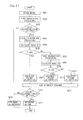
- FIG. 1 is a block diagram showing an example of a configuration of a production system according to an embodiment of the present invention
- FIG. 2 is a schematic view showing an example of a cylinder block according to the embodiment of the present invention.
- FIG. 3 is a schematic view showing an example of a configuration of a processing device according to the embodiment of the present invention.
- FIG. 4 is a sectional view showing an example of a sprayed coating including surface defects on an internal surface of a cylinder bore;
- FIG. 5 is a schematic view showing an example of a configuration of an imaging device according to the embodiment of the present invention.
- FIG. 6 is a graph showing an example of a relationship between a light quantity of pixels and a defect depth
- FIG. 7 is a graph showing an example of a relationship between a binarization threshold and a length of a defect detected
- FIG. 8 is a graph showing an example of a relationship between a binarization threshold and a length of detected defects having different depths
- FIG. 9 is a flowchart showing an example of a surface defect detection method according to the embodiment of the present invention.
- FIG. 10( a ) is a graph showing a relationship between a binarization threshold and a defect size according to a first modified example
- FIG. 10( b ) is a table showing determination results of a defect depth according to the first modified example
- FIG. 11 is a flowchart showing an example of a surface defect detection method according to the first modified example
- FIG. 12( a ) is a graph showing a relationship between a binarization threshold and a defect size according to a second modified example
- FIG. 12( b ) is a table showing determination results of a defect depth according to the second modified example.
- FIG. 13 is a flowchart showing an example of a surface defect detection method according to the second modified example.
- a production system includes a defect detection device 1 and a processing device 4 , as shown in FIG. 1 .
- the defect detection device 1 includes a control device 2 and an imaging device 3 .
- a cylinder block 101 includes a plurality of cylinder bores 102 of cylindrical holes for housing pistons.
- the processing device 4 used may be a plasma spraying device.
- the processing device (plasma spraying device) 4 includes a gun body 41 , and a spray gun 42 protruding at the lower portion of the gun body 41 .
- a bore spraying is obtained such that the gun body 41 moves in the direction of arrow A to enter a cylinder of the cylinder bore 102 of the cylinder block 101 , and rotates in the circumferential direction B.
- the spray gun 42 sprays a jet of metal or ceramics from the tip portion thereof onto the internal surface of the cylinder bore 102 of the cylinder block 101 so as to form a sprayed coating.
- the processing device 4 may be a device, such as a honing processing device, which may exert influence on surface defects of the sprayed coating, or may include several types of processing devices. Any device, as the processing device 4 , that exerts influence on surface defects may be used as appropriate depending on the inspection object.
- the sprayed coating is provided such that liquid droplets are applied to a surface in layers
- the sprayed coating typically creates a porous structure including a plurality of pores and minute defects derived from iron oxide, for example.
- the porous structure may lead to minute surface defects (pits) 104 provided on a surface 103 a because part of a surface layer of the sprayed coating 103 comes off when aftertreatment such as honing is performed after spraying, as schematically shown in FIG. 4 .
- the presence of casting cavities on the internal surface of the cylinder bore 102 also leads to surface defects (blowholes) on the surface 103 a because a sprayed coating is not appropriately applied to the surface of the blowholes.
- Examples of surface defects of the sprayed coating mainly include pits derived from aftertreatment, and blowholes derived from casting cavities, as described above.
- the diameter (maximum length) of blowholes is typically equivalent to or greater than the diameter (maximum length) of pits, and the depth of blowholes is typically five to ten times greater than the depth of pits.
- the surface defects of the sprayed coating 103 are not limited to pits and blowholes, but include recessed portions on the surface 103 a.
- the imaging device 3 shown in FIG. 1 , images a surface of the inspection object to obtain a two-dimensional image (a shaded image).
- the imaging device 3 includes a drive unit 30 , a light source 31 and a mirror 32 attached to the drive unit 30 , and an imaging unit 33 fixed above the drive unit 30 .
- the drive unit 30 enters the cylinder of the cylinder bore 102 as the inspection object, and rotates in the circumferential direction C.
- the light source 31 radiates the internal surface of the cylinder bore 102 with light.
- the mirror 32 reflects the light reflected from the inspection object to introduce the light into the imaging unit 33 .
- the imaging unit 33 is, for example, a CCD camera, and images the surface of the inspection object by receiving the reflected light from the mirror 32 , so as to obtain a two-dimensional image.
- the embodiment of the present invention exemplifies the imaging device 3 capable of imaging the internal surface of a cylindrical member such as the cylinder bore 102 , the configuration of the imaging device 3 may change depending on the inspection object.
- the two-dimensional image obtained by the imaging device 3 is a grayscale image with eight bits, for example, defined by the light quantity from black (0) to white (255) for each pixel.
- FIG. 6 shows an example of a relationship between the depth of surface defects of the sprayed coating and the light quantity of pixels.
- the reflected light from the inspection object is relatively bright at a normal position where there is no surface defect on the inspection object, and the light quantity of pixels in the image increases.
- the reflected light from the inspection object is relatively dark at a position where surface defects are present on the inspection object, and the light quantity of pixels in the image decreases.
- the light quantity of pixels in the image decreases.
- the control device 2 shown in FIG. 1 includes a central processing unit (CPU), a RAM, a ROM, and a hard disk, for example.
- the control device 2 functionally includes a binarization processing unit 11 , a ratio calculation unit 12 , a depth determination unit 13 , a volume calculation unit 14 , and a quality determination unit 15 .
- the binarization processing unit 11 implements binarization processing on the two-dimensional image obtained by the imaging unit 33 .
- binarization processing represents the processing of converting each pixel having the light quantity of a grayscale two-dimensional image into either white or black by use of a binarization threshold. As shown in FIG. 6 , when the light quantity of pixels is a predetermined binarization threshold Th or greater, the pixels are converted into white. When the light quantity of pixels is less than the predetermined binarization threshold Th, the pixels are converted into black. As the binarization threshold Th increases, the regions in black increase.
- FIG. 7 shows an example of variation in size (length) of a surface defect of the sprayed coating detected while changing a binarization threshold. As shown in FIG. 7 , as the binarization threshold is larger, the size of a detected defect corresponding to an aggregation of black regions in the image is larger. FIG. 7 further schematically shows images 11 to 13 after subjected to the binarization processing by use of different binarization thresholds. As shown in FIG. 7 , the size of the defect decreases in the order of the image 11 , the image 12 , and the image 13 . In the example shown in FIG.
- the binarization processing unit 11 detects defects each corresponding to an aggregation of black regions from each of the image after subjected to the first binarization processing and the image after subjected to the second binarization processing, and calculates the respective sizes for the same defect.
- the size of the defect includes at least one of the defect area or the defect length.
- the length of the defect calculated is a maximum length (greatest diameter), for example.
- the area of the defect calculated is an area of a circumcircle having the maximum length (greatest diameter), for example.
- the defect in the image subjected to the first binarization processing and the defect in the image subjected to the second binarization processing may be matched with each other by use of a positional coordinate.
- the size of the defect obtained by the first binarization processing by use of the first binarization threshold Th 1 is greater than the size of the defect obtained by the second binarization processing by use of the second binarization threshold Th 2 .
- FIG. 8 exemplifies a case in which there are a relatively deep defect A (such as a blowhole) and a relatively shallow defect B (such as a pit).
- the lengths of the detected defects A and B decrease as the respective binarization thresholds decrease, wherein a degree of variation of the lengths sharply increases from the respective particular inflection points P 1 and P 2 .
- the binarization processing unit 11 subjects the defect A to the binarization processing by use of the first binarization threshold Th 1 to detect a length XA 1 of the defect A.
- the binarization processing unit 11 then subjects the defect A to the binarization processing by use of the second binarization threshold Th 2 to detect a length XA 2 of the defect A.
- the binarization processing unit 11 further subjects the defect B to the binarization processing by use of the first binarization threshold Th 1 to detect a length XB 1 of the defect B.
- the binarization processing unit 11 then subjects the defect B to the binarization processing by use of the second binarization threshold Th 2 to detect a length XB 2 of the defect B.
- the size XA 2 is 0, and the ratio Y calculated results in 0. Since the size XA 1 obtained by the first binarization processing is greater than the size XA 2 obtained by the second binarization processing, the ratio Y is in the range of 0 or larger and 1 or smaller.
- the quality determination unit 15 determines whether the sum of the volumes of the defects calculated by the volume calculation unit 14 is an allowable value (threshold) or smaller.
- the quality determination unit 15 determines that the inspection object is fine when the sum of the volumes of the defects is the allowable value or smaller, and determines that the inspection object is inferior when the sum of the volumes of the defects is larger than the allowable value.
- the allowable value may be determined as appropriate depending on an allowable value of oil consumption, for example.
- the allowable value is preliminarily stored in the memory of the control device 2 , for example, and read out as necessary.
- the processing device 4 arranges processing conditions so that the sum of the volumes of the defects is the allowable value or smaller, based on the sum of the volumes of the defects calculated by the volume calculation unit 14 and the allowable value thereof.
- processing conditions for the processing process such as honing after plasma spray coating by the processing device 4 may also be arranged.
- step S 101 the imaging device 3 images a surface of the inspection object to obtain a two-dimensional image.
- step S 102 the binarization processing unit 11 subjects the two-dimensional image obtained by the imaging device 3 to the first binarization processing by use of the first binarization threshold Th 1 .
- the binarization processing unit 11 then extracts defects from the image subjected to the first binarization processing, so as to calculate the size X 1 of the defects.
- step S 104 the binarization processing unit 11 subjects the two-dimensional image obtained by the imaging device 3 to the second binarization processing by use of the second binarization threshold Th 2 .
- the binarization processing unit 11 then extracts defects from the image subjected to the second binarization processing, so as to calculate the size X 2 of the defects.
- step S 106 the depth determination unit 13 determines whether the ratio Y calculated by the ratio calculation unit 12 is the threshold N or smaller, so as to determine the relative depth of the defect.
- the depth determination unit 13 determines that the defect is shallow (as a pit, for example), and the process proceeds to step S 107 .
- step S 107 the volume calculation unit 14 sets the depth D 1 of the shallow defect. The volume calculation unit 14 further calculates the volume of the defect based on the depth D 1 of the shallow defect and the size X 1 of the defect.
- the depth determination unit 13 determines that the defect is deep (as a blowhole, for example) in step S 106 when the ratio Y is larger than the threshold N, and the process proceeds to step S 108 .
- the volume calculation unit 14 sets the depth D 2 of the defect determined as being deep to a larger value than the depth D 1 .
- the volume calculation unit 14 further calculates the volume of the defect based on the depth D 2 of the defect and the size X 1 of the defect.
- step S 109 the volume calculation unit 14 adds up the volumes of the all defects calculated in step S 107 and step S 108 to calculate the sum of the volumes of the defects.
- step S 110 the quality determination unit 15 determines whether the sum of the volumes of the defects calculated by the volume calculation unit 14 is the allowable value or smaller. The process proceeds to step S 111 when the sum of the volumes of the defects is the allowable value or smaller, and the quality determination unit 15 determines that the inspection object is fine and allowed to be marketed. When the sum of the volumes of the defects calculated by the volume calculation unit 14 is larger than the allowable value in step S 110 , the process proceeds to step S 112 , and the quality determination unit 15 determines that the inspection object is inferior.
- the embodiment of the present invention can determine the depth of each defect with high accuracy and calculate the volume of each defect with high accuracy.
- the quality of the product can be determined with high accuracy.
- a first modified example exemplifies a case in which the binarization processing is implemented three times, and the relative depth of each defect is evaluated in three stages.
- the binarization processing unit 11 implements (first to third) binarization processing three times by use of different first to third binarization thresholds, so as to calculate first to third sizes with respect to the same defect.
- FIG. 10( a ) exemplifies a case in which there are defects A, B, and C. As shown in FIG. 10( a ) , the length of the respective defects A to C linearly decreases as the binarization threshold decreases, and a degree of variation of the length sharply increases at the respective inflection points PA, PB, and PC.
- the binarization processing unit 11 subjects the respective defects A, B, and C to the binarization processing three times by use of the first to third binarization thresholds Th 1 to Th 3 , so as to calculate the sizes XA 1 , XA 2 , and XA 3 of the defect A, the sizes XB 1 , XB 2 , and XB 3 of the defect B, and the sizes XC 1 and XC 2 of the defect C.
- the defect C is not detected at the third binarization processing, and the size of the defect C calculated results in 0.
- the ratio calculation unit 12 repeats the same calculations for the defects B and C to obtain the respective first and second ratios, as in the case of the defect A.
- the depth determination unit 13 evaluates the relative depth of the surface defect based on the first and second ratios Y 1 and Y 2 in three stages. In particular, the depth determination unit 13 compares the first and second ratios Y 1 and Y 2 each with the threshold N, so as to determine the depth of the defect twice.
- the thresholds N used in the two determination steps may be the same or different from each other.
- the depth determination unit 13 comprehensively determines the depth of the defect based on the two determination results.
- the depth determination unit 13 determines whether the first ratio Y 1 is the threshold N or smaller in the first determination, and determines whether the second ratio Y 2 is the threshold N or smaller in the second determination. As shown in FIG. 10( b ) , since the two depth determination results for the defect A are both “deep”, the defect A is comprehensively determined as being the deepest. Since one of the two depth determination results for the defect B is “deep” and the other is “shallow”, the defect B is comprehensively determined as having an intermediate depth. Since the two depth determination results for the defect C are both “shallow”, the defect C is comprehensively determined as being the shallowest.
- the volume calculation unit 14 sets the depth of each defect in the three stages according to the determination results obtained by the depth determination unit 13 . For example, the volume calculation unit 14 sets the depth D 1 of the defect A determined as being the deepest to 10 ⁇ m, sets the depth D 2 of the defect B determined as having an intermediate depth to 50 ⁇ m, and sets the depth D 3 of the defect C determined as being the shallowest to 100 ⁇ m.
- step S 206 the depth determination unit 13 determines whether the first ratio Y 1 is the threshold N or smaller. When the first ratio Y 1 is the threshold N or smaller, the depth of the defect is determined as being the shallowest among the three stages, and the process proceeds to step S 207 , while skipping the third binarization processing.
- step S 207 the volume calculation unit 14 sets the depth D 1 of the defect determined as being the shallowest, and calculates the volume of the defect by use of the depth D 1 .
- step S 208 the binarization processing unit 11 implements the third binarization processing by use of the third binarization threshold Th 3 , and calculates the size X 3 of the defect.
- step S 210 it is determined whether the second ratio Y 2 is the threshold N or smaller.
- the depth of the defect is determined as being an intermediate level, and the process then proceeds to step S 211 .
- the volume calculation unit 14 sets the depth D 2 (>D 1 ) of the defect determined as being an intermediate level, and calculates the volume of the defect by use of the depth D 2 .
- the second ratio Y 2 is larger than the threshold N in step S 210
- the depth of the defect is determined as being the deepest, and the process then proceeds to step S 212 .
- the voltage calculation unit 14 sets the depth D 3 (>D 2 ) of the defect determined as being the deepest, and calculates the volume of the defect by use of the depth D 3 .
- step S 213 the sum of the volumes of the all defects obtained in step S 207 , step S 211 , and step S 212 is calculated.
- the process from step S 214 to step 216 is the same as the process from step S 110 to step S 112 shown in FIG. 9 , and the overlapping explanations are not repeated below.
- the binarization processing is implemented three times by use of the three different binarization thresholds to evaluate the depth of each defect in three stages, so as to calculate the volume of each defect with higher accuracy.
- the first modified example was illustrated by the three sets of the binarization processing, the first modified example may implement the binarization processing four times or more by use of four different binarization thresholds or more, so as to evaluate the depth of each defect in four stages or more.
- a second modified example exemplifies a case in which the depth of each defect is determined in several stages, while the binarization processing is implemented twice.
- the defects A, B, and C are each subjected to the binarization processing twice by use of the two binarization thresholds Th 1 and Th 2 , so as to calculate the sizes XA 1 and XA 2 of the defect A, the sizes XB 1 and XB 2 of the defect B, and the sizes XC 1 and XC 2 of the defect C.
- the ratio calculation unit 12 repeats the same calculation for the defects B and C to obtain the respective ratios, as in the case of the defect A.
- the depth determination unit 13 compares the ratio Y calculated by the ratio calculation unit 12 with each of multiple (two) different thresholds N 1 and N 2 , so as to determine the depth of each defect several times (twice).
- the thresholds N 1 and N 2 may be determined as appropriate depending on the product or the type of defects.
- the threshold N 1 is set to 0.5, for example.
- the threshold N 2 is set to 0.7, for example, which is larger than the threshold N 1 .
- the depth determination unit 13 determines whether the ratio Y is the threshold N 1 or smaller in the first determination, and determines whether the ratio Y is the threshold N 2 or smaller in the second determination.
- the depth determination unit 13 comprehensively determines the depth of each defect according to the two determination results.
- the defect A since the ratio Y is the threshold N 1 or smaller in the first determination, and the ratio Y is the threshold N 2 or smaller in the second determination, the defect A is comprehensively determined as being the deepest.
- the defect B since the ratio Y is larger than the threshold N 1 in the first determination, and the ratio Y is the threshold N 2 or smaller in the second determination, the defect B is comprehensively determined as having an intermediate depth.
- the defect C since the ratio Y is larger than the threshold N 1 in the first determination, and the ratio Y is larger than the threshold N 2 also in the second determination, the defect C is comprehensively determined as being the shallowest.
- the volume calculation unit 14 sets the depth of each defect in the three stages according to the determination results obtained by the depth determination unit 13 . For example, the volume calculation unit 14 sets the depth D 1 of the defect A determined as being the deepest to 10 ⁇ m, sets the depth D 2 of the defect B determined as having an intermediate depth to 50 ⁇ m, and sets the depth D 3 of the defect C determined as being the shallowest to 100 ⁇ m.
- step S 306 the depth determination unit 13 determines whether the ratio Y is the threshold N 1 or smaller. When the ratio Y is the threshold N 1 or smaller, the depth of the defect is determined as being the shallowest, and the process then proceeds to step S 307 .
- step S 307 the volume calculation unit 14 sets the depth D 1 of the defect determined as being the shallowest, and calculates the volume of the defect by use of the depth D 1 .
- step S 306 the process proceeds to step S 308 .
- step S 308 the depth determination unit 13 determines whether the ratio Y is the threshold N 2 or smaller, which is larger than the threshold N 1 .
- the process then proceeds to step S 309 .
- step S 309 the volume calculation unit 14 sets the depth D 2 (>D 1 ) of the defect determined as being an intermediate level, and calculates the volume of the defect by use of the depth D 2 .
- step S 308 When the ratio Y is larger than the threshold N 2 in step S 308 , the depth of the defect is determined as being the deepest, and the process then proceeds to step S 310 .
- step S 310 the voltage calculation unit 14 sets the depth D 3 (>D 2 ) of the defect determined as being the deepest, and calculates the volume of the defect by use of the depth D 3 .
- step S 311 the sum of the volumes of the all defects obtained in step S 307 , step S 309 , and step S 310 is calculated.
- step S 312 to step 314 is the same as the process from step S 110 to step S 112 shown in FIG. 9 , and the overlapping explanations are not repeated below.
- each defect is subjected to the depth determination twice by use of the different thresholds N 1 and N 2 to evaluate the depth of the defect in three stages, so as to obtain the depth and volume of the defect with higher accuracy.
- the second modified example was illustrated by the case in which each defect is subjected to the depth determination twice by use of the two thresholds N 1 and N 2 to comprehensively evaluate the depth of the defect in three stages, the second modified example is not limited thereto.
- the depth determination unit 13 may subject the defect to the depth determination three times or more in two stages by use of three different binarization thresholds or more, so as to comprehensively evaluate the depth of each in four stages or more.
- the embodiment of the present invention has exemplified the internal surface of the cylinder bore 102 of the cylinder block 101 of the engine, as an example of the inspection object by the defect detection device 1 , but is not limited thereto.
- the defect detection device 1 is applicable to various types of products which may have surface defects. Defects are not limited to any particular type, and the size of defects detected by use of binarization thresholds may vary linearly.
Applications Claiming Priority (1)
| Application Number | Priority Date | Filing Date | Title |
|---|---|---|---|
| PCT/JP2014/068193 WO2016006039A1 (ja) | 2014-07-08 | 2014-07-08 | 欠陥検査装置及び生産システム |
Related Parent Applications (1)
| Application Number | Title | Priority Date | Filing Date |
|---|---|---|---|
| PCT/JP2014/068193 A-371-Of-International WO2016006039A1 (ja) | 2014-07-08 | 2014-07-08 | 欠陥検査装置及び生産システム |
Related Child Applications (1)
| Application Number | Title | Priority Date | Filing Date |
|---|---|---|---|
| US15/720,077 Division US10339645B2 (en) | 2014-07-08 | 2017-09-29 | Defect detection device and production system |
Publications (2)
| Publication Number | Publication Date |
|---|---|
| US20170161886A1 US20170161886A1 (en) | 2017-06-08 |
| US9805457B2 true US9805457B2 (en) | 2017-10-31 |
Family
ID=55063715
Family Applications (2)
| Application Number | Title | Priority Date | Filing Date |
|---|---|---|---|
| US15/324,250 Active US9805457B2 (en) | 2014-07-08 | 2014-07-08 | Defect detection device and production system |
| US15/720,077 Active 2034-08-19 US10339645B2 (en) | 2014-07-08 | 2017-09-29 | Defect detection device and production system |
Family Applications After (1)
| Application Number | Title | Priority Date | Filing Date |
|---|---|---|---|
| US15/720,077 Active 2034-08-19 US10339645B2 (en) | 2014-07-08 | 2017-09-29 | Defect detection device and production system |
Country Status (8)
| Country | Link |
|---|---|
| US (2) | US9805457B2 (ja) |
| EP (1) | EP3168569B1 (ja) |
| JP (1) | JP6288272B2 (ja) |
| KR (1) | KR101730787B1 (ja) |
| CN (1) | CN106471333B (ja) |
| ES (1) | ES2705076T3 (ja) |
| MX (1) | MX354715B (ja) |
| WO (1) | WO2016006039A1 (ja) |
Families Citing this family (15)
| Publication number | Priority date | Publication date | Assignee | Title |
|---|---|---|---|---|
| WO2016006039A1 (ja) * | 2014-07-08 | 2016-01-14 | 日産自動車株式会社 | 欠陥検査装置及び生産システム |
| WO2018012192A1 (ja) * | 2016-07-12 | 2018-01-18 | 吉野石膏株式会社 | 検査方法、検査・通知方法、該検査方法を含む製造方法、検査装置及び製造装置 |
| US10562244B2 (en) * | 2017-01-23 | 2020-02-18 | The Boeing Company | Systems and methods for forming a composite part based on volume |
| CN106996749A (zh) * | 2017-03-31 | 2017-08-01 | 西安理工大学 | 管内周向环形窄沟槽几何参数检测装置及检测方法 |
| HUE042725T2 (hu) * | 2017-05-18 | 2019-07-29 | Grob Gmbh & Co Kg | Eljárás és készülék bevont felületek minõségének vizsgálatára |
| CN108961252B (zh) * | 2018-07-27 | 2021-06-08 | Oppo(重庆)智能科技有限公司 | 检测logo粘贴不良的方法、电子装置及计算机可读存储介质 |
| CN109283182A (zh) * | 2018-08-03 | 2019-01-29 | 江苏理工学院 | 一种电池焊点缺陷的检测方法、装置及系统 |
| JP2020038085A (ja) * | 2018-09-03 | 2020-03-12 | Juki株式会社 | 検査装置 |
| CN110148106B (zh) * | 2019-01-18 | 2023-06-27 | 华晨宝马汽车有限公司 | 一种利用深度学习模型检测物体表面缺陷的系统及方法 |
| US11176660B2 (en) * | 2019-07-25 | 2021-11-16 | Caterpillar Inc. | Sorting pistons with flaws |
| CN112388391B (zh) * | 2020-11-09 | 2022-08-23 | 上海圣之尧智能科技有限公司 | 一种车削刀具置换方法 |
| CN114392875A (zh) * | 2021-12-15 | 2022-04-26 | 邳州通达化工机械有限公司 | 一种避免安全隐患的化工设备搪瓷层紧急修补装置 |
| CN114459362B (zh) * | 2021-12-31 | 2024-03-26 | 深圳市瑞图生物技术有限公司 | 一种测量装置及其测量方法 |
| CN114952456A (zh) * | 2022-07-28 | 2022-08-30 | 常州市旭泉精密电机有限公司 | 电机轴磨削加工用智能化自动校测装置 |
| CN116571410B (zh) * | 2023-07-14 | 2023-09-26 | 杭州百子尖科技股份有限公司 | 基于机器视觉的缺陷区域修复方法、装置、设备以及介质 |
Citations (18)
| Publication number | Priority date | Publication date | Assignee | Title |
|---|---|---|---|---|
| JPH04169807A (ja) | 1990-11-01 | 1992-06-17 | Fuji Xerox Co Ltd | 表面傷検査装置 |
| US5196716A (en) * | 1990-05-21 | 1993-03-23 | Mitsui Mining & Smelting Co., Ltd. | Method and apparatus for measuring internal defects for position and depth |
| JPH05322792A (ja) | 1992-05-18 | 1993-12-07 | Omron Corp | 欠陥検査装置 |
| JPH10171981A (ja) | 1996-12-04 | 1998-06-26 | Suzuki Motor Corp | 刻印文字二値化装置 |
| JPH1123477A (ja) | 1997-06-27 | 1999-01-29 | Toyota Motor Corp | 円筒内面の検査装置 |
| JP2002324233A (ja) | 2001-04-25 | 2002-11-08 | Showa Corp | パイプの割れ検出方法及び装置 |
| US6734960B1 (en) * | 1999-06-09 | 2004-05-11 | Toshiba Ceramics Co., Ltd. | Wafer defect measuring method and apparatus |
| JP2005069887A (ja) | 2003-08-25 | 2005-03-17 | Nippon Steel Corp | 欠陥検査方法及び装置 |
| JP2005121450A (ja) | 2003-10-16 | 2005-05-12 | Hitachi Ltd | 欠陥検査装置及びその方法並びに円筒物体の内面加工方法 |
| US20070052795A1 (en) * | 2005-09-02 | 2007-03-08 | Swanger Michael E | System and method for evaluating a machined surface of a cast metal component |
| US20090087079A1 (en) * | 2007-09-27 | 2009-04-02 | Fujifilm Corporation | Defect detecting apparatus and method |
| JP2010238305A (ja) | 2009-03-31 | 2010-10-21 | Sharp Corp | 情報記録装置および情報記録方法 |
| JP2010276347A (ja) | 2009-05-26 | 2010-12-09 | Honda Motor Co Ltd | 表面検査装置 |
| JP2011232070A (ja) | 2010-04-26 | 2011-11-17 | Seiko Epson Corp | 凹部深さの測定方法及び検査装置 |
| US20120062728A1 (en) | 2009-05-21 | 2012-03-15 | Honda Motor Co., Ltd. | Surface inspecting device |
| JP2012237585A (ja) | 2011-05-10 | 2012-12-06 | Toppan Printing Co Ltd | 欠陥検査方法 |
| US20130155061A1 (en) * | 2011-12-16 | 2013-06-20 | University Of Southern California | Autonomous pavement condition assessment |
| US20130261989A1 (en) * | 2012-03-29 | 2013-10-03 | General Electric Company | Flaw detection using transient thermography |
Family Cites Families (10)
| Publication number | Priority date | Publication date | Assignee | Title |
|---|---|---|---|---|
| JP2771190B2 (ja) * | 1988-10-07 | 1998-07-02 | 株式会社日立製作所 | スルーホール充填状態検査方法およびその装置 |
| JP3331127B2 (ja) * | 1995-08-22 | 2002-10-07 | 株式会社東芝 | マスク欠陥修正装置および修正方法 |
| US6779159B2 (en) * | 2001-06-08 | 2004-08-17 | Sumitomo Mitsubishi Silicon Corporation | Defect inspection method and defect inspection apparatus |
| JP3993817B2 (ja) * | 2002-12-11 | 2007-10-17 | 株式会社日立製作所 | 欠陥組成分析方法及び装置 |
| JP2007071661A (ja) * | 2005-09-06 | 2007-03-22 | Sumitomo Electric Ind Ltd | 外観検査装置 |
| US7903864B1 (en) * | 2007-01-17 | 2011-03-08 | Matrox Electronic Systems, Ltd. | System and methods for the detection of irregularities in objects based on an image of the object |
| JP4898713B2 (ja) * | 2008-01-17 | 2012-03-21 | 株式会社日立ハイテクノロジーズ | 表面検査装置および表面検査方法 |
| JP5664152B2 (ja) * | 2009-12-25 | 2015-02-04 | 株式会社リコー | 撮像装置、車載用撮像システム及び物体識別装置 |
| CN102589461A (zh) * | 2012-01-17 | 2012-07-18 | 华中科技大学 | 一种基于图像的积雪深度测量方法 |
| WO2016006039A1 (ja) * | 2014-07-08 | 2016-01-14 | 日産自動車株式会社 | 欠陥検査装置及び生産システム |
-
2014
- 2014-07-08 WO PCT/JP2014/068193 patent/WO2016006039A1/ja active Application Filing
- 2014-07-08 CN CN201480080388.9A patent/CN106471333B/zh active Active
- 2014-07-08 EP EP14897276.3A patent/EP3168569B1/en active Active
- 2014-07-08 MX MX2017000069A patent/MX354715B/es active IP Right Grant
- 2014-07-08 ES ES14897276T patent/ES2705076T3/es active Active
- 2014-07-08 US US15/324,250 patent/US9805457B2/en active Active
- 2014-07-08 JP JP2016532820A patent/JP6288272B2/ja active Active
- 2014-07-08 KR KR1020167035897A patent/KR101730787B1/ko active IP Right Grant
-
2017
- 2017-09-29 US US15/720,077 patent/US10339645B2/en active Active
Patent Citations (19)
| Publication number | Priority date | Publication date | Assignee | Title |
|---|---|---|---|---|
| US5196716A (en) * | 1990-05-21 | 1993-03-23 | Mitsui Mining & Smelting Co., Ltd. | Method and apparatus for measuring internal defects for position and depth |
| JPH04169807A (ja) | 1990-11-01 | 1992-06-17 | Fuji Xerox Co Ltd | 表面傷検査装置 |
| JPH05322792A (ja) | 1992-05-18 | 1993-12-07 | Omron Corp | 欠陥検査装置 |
| JPH10171981A (ja) | 1996-12-04 | 1998-06-26 | Suzuki Motor Corp | 刻印文字二値化装置 |
| JPH1123477A (ja) | 1997-06-27 | 1999-01-29 | Toyota Motor Corp | 円筒内面の検査装置 |
| US6734960B1 (en) * | 1999-06-09 | 2004-05-11 | Toshiba Ceramics Co., Ltd. | Wafer defect measuring method and apparatus |
| JP2002324233A (ja) | 2001-04-25 | 2002-11-08 | Showa Corp | パイプの割れ検出方法及び装置 |
| JP2005069887A (ja) | 2003-08-25 | 2005-03-17 | Nippon Steel Corp | 欠陥検査方法及び装置 |
| JP2005121450A (ja) | 2003-10-16 | 2005-05-12 | Hitachi Ltd | 欠陥検査装置及びその方法並びに円筒物体の内面加工方法 |
| US20070052795A1 (en) * | 2005-09-02 | 2007-03-08 | Swanger Michael E | System and method for evaluating a machined surface of a cast metal component |
| US20090087079A1 (en) * | 2007-09-27 | 2009-04-02 | Fujifilm Corporation | Defect detecting apparatus and method |
| JP2009085617A (ja) | 2007-09-27 | 2009-04-23 | Fujifilm Corp | 欠陥検出装置及び方法 |
| JP2010238305A (ja) | 2009-03-31 | 2010-10-21 | Sharp Corp | 情報記録装置および情報記録方法 |
| US20120062728A1 (en) | 2009-05-21 | 2012-03-15 | Honda Motor Co., Ltd. | Surface inspecting device |
| JP2010276347A (ja) | 2009-05-26 | 2010-12-09 | Honda Motor Co Ltd | 表面検査装置 |
| JP2011232070A (ja) | 2010-04-26 | 2011-11-17 | Seiko Epson Corp | 凹部深さの測定方法及び検査装置 |
| JP2012237585A (ja) | 2011-05-10 | 2012-12-06 | Toppan Printing Co Ltd | 欠陥検査方法 |
| US20130155061A1 (en) * | 2011-12-16 | 2013-06-20 | University Of Southern California | Autonomous pavement condition assessment |
| US20130261989A1 (en) * | 2012-03-29 | 2013-10-03 | General Electric Company | Flaw detection using transient thermography |
Also Published As
| Publication number | Publication date |
|---|---|
| US20180025486A1 (en) | 2018-01-25 |
| US20170161886A1 (en) | 2017-06-08 |
| CN106471333B (zh) | 2018-01-23 |
| EP3168569A1 (en) | 2017-05-17 |
| CN106471333A (zh) | 2017-03-01 |
| MX354715B (es) | 2018-03-16 |
| EP3168569A4 (en) | 2017-11-22 |
| KR101730787B1 (ko) | 2017-04-27 |
| KR20170012377A (ko) | 2017-02-02 |
| MX2017000069A (es) | 2017-04-27 |
| WO2016006039A1 (ja) | 2016-01-14 |
| EP3168569B1 (en) | 2018-10-24 |
| JPWO2016006039A1 (ja) | 2017-04-27 |
| JP6288272B2 (ja) | 2018-03-07 |
| ES2705076T3 (es) | 2019-03-21 |
| US10339645B2 (en) | 2019-07-02 |
Similar Documents
| Publication | Publication Date | Title |
|---|---|---|
| US10339645B2 (en) | Defect detection device and production system | |
| US11931955B2 (en) | Method for evaluating the quality of a component produced by an additive sintering and/or melting method | |
| US8942837B2 (en) | Method for inspecting a manufacturing device | |
| EP3398701A3 (en) | Real time detection of defects during formation of an additively manufactured component | |
| US20160297148A1 (en) | Method for evaluating at least one component layer manufactured by means of an additive powder layer method | |
| WO2018016102A1 (ja) | 形状測定装置及び形状測定方法 | |
| CN110906875A (zh) | 一种孔径测量的视觉处理方法 | |
| US20190308762A1 (en) | Inspection device and production management method | |
| KR101452896B1 (ko) | 분무이미지 처리시스템 및 그 방법 | |
| KR101426484B1 (ko) | 분무이미지 처리시스템 및 그 방법 | |
| EP3298583B1 (en) | Methods for inspecting cellular articles | |
| US20180100225A1 (en) | Thermal spraying method | |
| CN115187607A (zh) | 一种基于图像处理的喷油器喷雾形态检测方法 | |
| CN114897853A (zh) | 用于晶圆的检测方法、检测装置及存储介质 | |
| CN104423002A (zh) | 镜头模组的测量方法 | |
| CN109636750B (zh) | 一种针对铁轨轮廓曲线图像的动态局域二值化方法 | |
| JP6056374B2 (ja) | 塗布状態検査装置及び方法 | |
| JP6373743B2 (ja) | 面の評価方法および面の評価装置 | |
| JP2012093200A (ja) | 表面評価装置 | |
| JP2004132900A (ja) | エンジンボア内周面評価装置 | |
| CN111609827B (zh) | 发动机缸体的理论精基准面的构建方法以及发动机缸体 | |
| JP2023049683A (ja) | 表面欠陥検査装置及び表面欠陥検査方法 | |
| Miszczak | Structure analysis of the surface of plunger and barrel assembly in the injection pump pumping section | |
| ITMO20060093A1 (it) | Metodo per l'individuazione di aree di disuniformita' su una superficie | |
| CN114021274A (zh) | 超声波冲头使用寿命检测方法、系统、装置及存储介质 |
Legal Events
| Date | Code | Title | Description |
|---|---|---|---|
| AS | Assignment |
Owner name: NISSAN MOTOR CO., LTD., JAPAN Free format text: ASSIGNMENT OF ASSIGNORS INTEREST;ASSIGNORS:SHIBAYAMA, HIROHISA;SHIOTANI, EIJI;SAKURAI, SATORU;AND OTHERS;SIGNING DATES FROM 20161107 TO 20161219;REEL/FRAME:040895/0866 |
|
| STCF | Information on status: patent grant |
Free format text: PATENTED CASE |
|
| MAFP | Maintenance fee payment |
Free format text: PAYMENT OF MAINTENANCE FEE, 4TH YEAR, LARGE ENTITY (ORIGINAL EVENT CODE: M1551); ENTITY STATUS OF PATENT OWNER: LARGE ENTITY Year of fee payment: 4 |