US9795983B2 - Mask assembly for testing a deposition process, deposition apparatus including the mask assembly, and testing method for a deposition process using the mask assembly - Google Patents
Mask assembly for testing a deposition process, deposition apparatus including the mask assembly, and testing method for a deposition process using the mask assembly Download PDFInfo
- Publication number
- US9795983B2 US9795983B2 US13/794,701 US201313794701A US9795983B2 US 9795983 B2 US9795983 B2 US 9795983B2 US 201313794701 A US201313794701 A US 201313794701A US 9795983 B2 US9795983 B2 US 9795983B2
- Authority
- US
- United States
- Prior art keywords
- deposition
- mask assembly
- base substrate
- opening
- shutter member
- Prior art date
- Legal status (The legal status is an assumption and is not a legal conclusion. Google has not performed a legal analysis and makes no representation as to the accuracy of the status listed.)
- Active, expires
Links
Images


Classifications
-
- C—CHEMISTRY; METALLURGY
- C23—COATING METALLIC MATERIAL; COATING MATERIAL WITH METALLIC MATERIAL; CHEMICAL SURFACE TREATMENT; DIFFUSION TREATMENT OF METALLIC MATERIAL; COATING BY VACUUM EVAPORATION, BY SPUTTERING, BY ION IMPLANTATION OR BY CHEMICAL VAPOUR DEPOSITION, IN GENERAL; INHIBITING CORROSION OF METALLIC MATERIAL OR INCRUSTATION IN GENERAL
- C23C—COATING METALLIC MATERIAL; COATING MATERIAL WITH METALLIC MATERIAL; SURFACE TREATMENT OF METALLIC MATERIAL BY DIFFUSION INTO THE SURFACE, BY CHEMICAL CONVERSION OR SUBSTITUTION; COATING BY VACUUM EVAPORATION, BY SPUTTERING, BY ION IMPLANTATION OR BY CHEMICAL VAPOUR DEPOSITION, IN GENERAL
- C23C14/00—Coating by vacuum evaporation, by sputtering or by ion implantation of the coating forming material
- C23C14/04—Coating on selected surface areas, e.g. using masks
- C23C14/042—Coating on selected surface areas, e.g. using masks using masks
-
- B—PERFORMING OPERATIONS; TRANSPORTING
- B05—SPRAYING OR ATOMISING IN GENERAL; APPLYING FLUENT MATERIALS TO SURFACES, IN GENERAL
- B05C—APPARATUS FOR APPLYING FLUENT MATERIALS TO SURFACES, IN GENERAL
- B05C3/00—Apparatus in which the work is brought into contact with a bulk quantity of liquid or other fluent material
- B05C3/20—Apparatus in which the work is brought into contact with a bulk quantity of liquid or other fluent material for applying liquid or other fluent material only at particular parts of the work
-
- C—CHEMISTRY; METALLURGY
- C23—COATING METALLIC MATERIAL; COATING MATERIAL WITH METALLIC MATERIAL; CHEMICAL SURFACE TREATMENT; DIFFUSION TREATMENT OF METALLIC MATERIAL; COATING BY VACUUM EVAPORATION, BY SPUTTERING, BY ION IMPLANTATION OR BY CHEMICAL VAPOUR DEPOSITION, IN GENERAL; INHIBITING CORROSION OF METALLIC MATERIAL OR INCRUSTATION IN GENERAL
- C23C—COATING METALLIC MATERIAL; COATING MATERIAL WITH METALLIC MATERIAL; SURFACE TREATMENT OF METALLIC MATERIAL BY DIFFUSION INTO THE SURFACE, BY CHEMICAL CONVERSION OR SUBSTITUTION; COATING BY VACUUM EVAPORATION, BY SPUTTERING, BY ION IMPLANTATION OR BY CHEMICAL VAPOUR DEPOSITION, IN GENERAL
- C23C14/00—Coating by vacuum evaporation, by sputtering or by ion implantation of the coating forming material
- C23C14/22—Coating by vacuum evaporation, by sputtering or by ion implantation of the coating forming material characterised by the process of coating
- C23C14/24—Vacuum evaporation
-
- C—CHEMISTRY; METALLURGY
- C23—COATING METALLIC MATERIAL; COATING MATERIAL WITH METALLIC MATERIAL; CHEMICAL SURFACE TREATMENT; DIFFUSION TREATMENT OF METALLIC MATERIAL; COATING BY VACUUM EVAPORATION, BY SPUTTERING, BY ION IMPLANTATION OR BY CHEMICAL VAPOUR DEPOSITION, IN GENERAL; INHIBITING CORROSION OF METALLIC MATERIAL OR INCRUSTATION IN GENERAL
- C23C—COATING METALLIC MATERIAL; COATING MATERIAL WITH METALLIC MATERIAL; SURFACE TREATMENT OF METALLIC MATERIAL BY DIFFUSION INTO THE SURFACE, BY CHEMICAL CONVERSION OR SUBSTITUTION; COATING BY VACUUM EVAPORATION, BY SPUTTERING, BY ION IMPLANTATION OR BY CHEMICAL VAPOUR DEPOSITION, IN GENERAL
- C23C14/00—Coating by vacuum evaporation, by sputtering or by ion implantation of the coating forming material
- C23C14/22—Coating by vacuum evaporation, by sputtering or by ion implantation of the coating forming material characterised by the process of coating
- C23C14/34—Sputtering
- C23C14/46—Sputtering by ion beam produced by an external ion source
-
- C—CHEMISTRY; METALLURGY
- C23—COATING METALLIC MATERIAL; COATING MATERIAL WITH METALLIC MATERIAL; CHEMICAL SURFACE TREATMENT; DIFFUSION TREATMENT OF METALLIC MATERIAL; COATING BY VACUUM EVAPORATION, BY SPUTTERING, BY ION IMPLANTATION OR BY CHEMICAL VAPOUR DEPOSITION, IN GENERAL; INHIBITING CORROSION OF METALLIC MATERIAL OR INCRUSTATION IN GENERAL
- C23C—COATING METALLIC MATERIAL; COATING MATERIAL WITH METALLIC MATERIAL; SURFACE TREATMENT OF METALLIC MATERIAL BY DIFFUSION INTO THE SURFACE, BY CHEMICAL CONVERSION OR SUBSTITUTION; COATING BY VACUUM EVAPORATION, BY SPUTTERING, BY ION IMPLANTATION OR BY CHEMICAL VAPOUR DEPOSITION, IN GENERAL
- C23C14/00—Coating by vacuum evaporation, by sputtering or by ion implantation of the coating forming material
- C23C14/22—Coating by vacuum evaporation, by sputtering or by ion implantation of the coating forming material characterised by the process of coating
- C23C14/52—Means for observation of the coating process
-
- C—CHEMISTRY; METALLURGY
- C23—COATING METALLIC MATERIAL; COATING MATERIAL WITH METALLIC MATERIAL; CHEMICAL SURFACE TREATMENT; DIFFUSION TREATMENT OF METALLIC MATERIAL; COATING BY VACUUM EVAPORATION, BY SPUTTERING, BY ION IMPLANTATION OR BY CHEMICAL VAPOUR DEPOSITION, IN GENERAL; INHIBITING CORROSION OF METALLIC MATERIAL OR INCRUSTATION IN GENERAL
- C23C—COATING METALLIC MATERIAL; COATING MATERIAL WITH METALLIC MATERIAL; SURFACE TREATMENT OF METALLIC MATERIAL BY DIFFUSION INTO THE SURFACE, BY CHEMICAL CONVERSION OR SUBSTITUTION; COATING BY VACUUM EVAPORATION, BY SPUTTERING, BY ION IMPLANTATION OR BY CHEMICAL VAPOUR DEPOSITION, IN GENERAL
- C23C14/00—Coating by vacuum evaporation, by sputtering or by ion implantation of the coating forming material
- C23C14/22—Coating by vacuum evaporation, by sputtering or by ion implantation of the coating forming material characterised by the process of coating
- C23C14/54—Controlling or regulating the coating process
- C23C14/542—Controlling the film thickness or evaporation rate
-
- C—CHEMISTRY; METALLURGY
- C23—COATING METALLIC MATERIAL; COATING MATERIAL WITH METALLIC MATERIAL; CHEMICAL SURFACE TREATMENT; DIFFUSION TREATMENT OF METALLIC MATERIAL; COATING BY VACUUM EVAPORATION, BY SPUTTERING, BY ION IMPLANTATION OR BY CHEMICAL VAPOUR DEPOSITION, IN GENERAL; INHIBITING CORROSION OF METALLIC MATERIAL OR INCRUSTATION IN GENERAL
- C23C—COATING METALLIC MATERIAL; COATING MATERIAL WITH METALLIC MATERIAL; SURFACE TREATMENT OF METALLIC MATERIAL BY DIFFUSION INTO THE SURFACE, BY CHEMICAL CONVERSION OR SUBSTITUTION; COATING BY VACUUM EVAPORATION, BY SPUTTERING, BY ION IMPLANTATION OR BY CHEMICAL VAPOUR DEPOSITION, IN GENERAL
- C23C14/00—Coating by vacuum evaporation, by sputtering or by ion implantation of the coating forming material
- C23C14/22—Coating by vacuum evaporation, by sputtering or by ion implantation of the coating forming material characterised by the process of coating
- C23C14/56—Apparatus specially adapted for continuous coating; Arrangements for maintaining the vacuum, e.g. vacuum locks
- C23C14/568—Transferring the substrates through a series of coating stations
Definitions
- aspects of embodiments of the present invention relate to a mask assembly for testing a deposition process, a deposition apparatus including the mask assembly, and a testing method for a deposition process using the mask assembly.
- a flat panel display or a semiconductor device may be manufactured by depositing organic or inorganic materials on a base substrate.
- a deposition process may be performed in a deposition apparatus.
- the deposition apparatus may include a vacuum chamber, at least one deposition source in the vacuum chamber, a mask, and a transfer unit that transfers the base substrate.
- a testing of the deposition process may be performed to assess whether the deposition process (as performed in the deposition apparatus) is appropriate before performing the deposition process to manufacture the flat panel display or the semiconductor device.
- a test substrate may be used to test the deposition process. For example, the thickness and uniformity of the deposited material may be measured on the test substrate as part of the testing of the deposition process. To this end, the measured thickness and uniformity may be compared to a reference thickness and uniformity.
- test substrates When testing the deposition process for a deposition apparatus having multiple deposition sources, each for depositing a different material, multiple test substrates may be needed. For example, the test substrates may be sequentially loaded into the deposition apparatus and the different materials respectively deposited on the different test substrates. The thickness and uniformity of each of the deposition materials deposited on the respective test substrates may then be measured.
- Embodiments of the present invention provide for a mask assembly capable of testing a deposition process using one test substrate for a plurality of deposition sources. Further embodiments provide for a deposition apparatus including the mask assembly, and for a testing method for a deposition process using the mask assembly.
- a mask assembly for testing a deposition process includes a support member having a first opening configured to allow deposition materials to pass through while supporting a base substrate on which the passed-through deposition materials are deposited while the mask assembly moves in a first direction, a shutter member accommodated in the support member and having a second opening smaller than the first opening, and a drive member configured to move the shutter member in accordance with the movement of the mask assembly to change a position of the second opening with respect to the base substrate.
- the support member may include a bottom portion having the first opening, and a sidewall bent from the bottom portion to support the base substrate.
- the shutter member may be configured to move with respect to the base substrate in a direction opposite to the first direction in accordance with the movement of the mask assembly.
- the second opening may extend in a second direction substantially perpendicular to the first direction.
- the shutter member may have a larger area than the first opening and may be located on the bottom portion.
- the mask assembly may further include a rail unit located on the bottom portion, and a coupling unit coupled to the shutter member and inserted into the rail unit to allow the shutter member to move along the rail unit.
- the drive member may be configured to rotate in accordance with the movement of the mask assembly.
- the shutter member may be configured to move in accordance with the rotation of the drive member.
- the drive member may include a first pinion configured to rotate by a frictional force.
- the drive member may further include a second pinion configured to receive a motive power from the first pinion and to make contact with a side surface of the shutter member.
- the shutter member may include sawteeth on the side surface of the shutter member and configured to engage sawteeth of the second pinion.
- the drive member may include an N-polar portion and an S-polar portion that are alternately arranged, and may be configured to rotate by a magnetic force.
- a mask assembly for testing a deposition process includes a support member having a first opening configured to pass through deposition materials while supporting a base substrate on which the passed-through deposition materials are deposited while the mask assembly moves, a shutter member accommodated in the support member and including a rotatable member having a second opening smaller than the first opening, and a drive member configured to rotate the rotatable member in accordance with the movement of the mask assembly to change a position of the second opening with respect to the base substrate.
- the support member may include a bottom portion having the first opening, and a sidewall bent from the bottom portion to support the base substrate.
- the shutter member may further include a rotation axis coupled to the rotatable member to rotate the rotatable member.
- the first opening may include a left first opening and a right first opening.
- the shutter member may include a left shutter member overlapping the left first opening and a right shutter member overlapping the right first opening.
- the drive member may include a first drive member configured to rotate in a first direction and a second drive member configured to rotate in a second direction that is opposite to the first direction in accordance, with the movement of the support member.
- the position of the second opening of the rotatable member of the left shutter member with respect to the base substrate may be configured to change by the rotation of the first drive member.
- the position of the second opening of the rotatable member of the right shutter member with respect to the base substrate may be configured to change by the rotation of the second drive member.
- Each of the first drive member and the second drive member may include a first pinion configured to rotate by a frictional force.
- Each of the first and second drive members may further include a second pinion configured to receive a motive power from the first pinion and to make contact with a side surface of the shutter member.
- Each of the first and second drive members may include a discus-shaped magnetic member including an N-polar portion and an S-polar portion that are alternately arranged.
- the magnetic member may be configured to rotate by a magnetic force.
- a deposition apparatus includes: a plurality of deposition sources configured to deposit deposition materials; a deposition chamber accommodating the deposition sources; a mask assembly for testing a deposition process, the mask assembly being configured to couple to a base substrate while moving through the deposition chamber while the deposition sources deposit the deposition materials on the base substrate; and a transfer unit configured to move the mask assembly through the deposition chamber.
- the mask assembly includes a support member having a first opening configured to allow the deposition materials to pass through while supporting the base substrate on which the passed-through deposition materials are deposited, a shutter member accommodated in the support member and having a second opening smaller than the first opening, and a drive member configured to change a position of the second opening with respect to the base substrate in accordance with the movement of the mask assembly.
- the transfer unit may include a plurality of rollers configured to move the mask assembly through the deposition chamber.
- the drive member may be configured to rotate in accordance with the movement of the mask assembly.
- the position of the second opening may be configured to change by the rotation of the drive member.
- the deposition chamber may include a loading area configured to couple the base substrate to the mask assembly, a deposition area in which the deposition sources are accommodated, and an unloading area configured to decouple the base substrate from the mask assembly.
- the drive member may include a plurality of pinions.
- One of the pinions may be configured to contact a side surface of the shutter member to change the position of the second opening with respect to the base substrate.
- the deposition chamber may include a plurality of transfer racks on a sidewall of the deposition area to correspond to the deposition sources or to spaces between the deposition sources.
- Another one of the pinions may be configured to contact the transfer racks to change the position of the second opening with respect to the base substrate.
- the deposition apparatus may further include a return unit configured to return the mask assembly to the loading area from the unloading area, and a return chamber accommodating the return unit.
- the return chamber may include a return rack on a sidewall of the return chamber.
- the drive member may include a discus-shaped magnetic member including an N-polar portion and an S-polar portion that are alternately arranged.
- the deposition chamber may include a plurality of magnetic transfer members, each including an N-polar portion and an S-polar portion that are alternately arranged, on a sidewall of the deposition area to correspond to the deposition sources.
- the support member may include a bottom portion having the first opening, and a sidewall bent from the bottom portion to support the base substrate.
- the shutter member may be configured to move with respect to the base substrate in a direction opposite to a direction in which the mask assembly moves, in accordance with the movement of the mask assembly.
- the shutter member may include a rotatable member configured to rotate by the movement of the mask assembly.
- a testing method for a deposition process using a mask assembly includes: entering the mask assembly into a deposition area of a deposition chamber accommodating a plurality of deposition sources, the mask assembly including a support member supporting a base substrate and a shutter member having an opening; depositing a respective plurality of deposition materials from the plurality of deposition sources onto the base substrate; moving the mask assembly through the deposition area; and changing a position of the opening of the shutter member with respect to the base substrate in accordance with the movement of the mask assembly.
- the testing method may further include: exiting the mask assembly from the deposition area, and returning the mask assembly to an entrance of the deposition area from an exit of the deposition area.
- the changing of the position of the opening of the shutter member may include moving the shutter member with respect to the base substrate in a direction opposite to a direction in which the mask assembly moves.
- the changing of the position of the opening of the shutter member may include rotating the shutter member in accordance with the movement of the mask assembly.
- the plurality of deposition materials may include a corresponding plurality of different deposition materials.
- the mask assembly uses one test substrate to test the deposition process of the deposition apparatus having multiple deposition sources supplying a corresponding multiple deposition materials.
- the mask assembly receives the respective deposition materials in different areas of the test substrate. Since the number of test substrates needed to test the deposition process may be reduced, testing costs may be reduced and the time needed to test the deposition process may be shortened.
- the position of the second opening of the shutter member with respect to the test substrate is changed in accordance with the movement of the mask assembly.
- the position of the second opening is changed for each deposition source.
- the deposition materials are deposited in different areas of the test substrate.
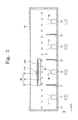
- FIG. 1 is a plan view showing a deposition apparatus according to an exemplary embodiment of the present invention
- FIG. 2 is a first cross-sectional view showing a portion of the deposition apparatus shown in FIG. 1 according to an exemplary embodiment of the present invention
- FIG. 3 is a second cross-sectional view showing a portion of the deposition apparatus shown in FIGS. 1-2 ;
- FIG. 4A is a perspective view showing a mask assembly used to test a deposition process according to an exemplary embodiment of the present invention
- FIG. 4B is an exploded perspective view showing the mask assembly of FIG. 4A ;
- FIG. 5A is a perspective view showing a mask assembly used to test a deposition process according to another exemplary embodiment of the present invention.
- FIG. 5B is an exploded perspective view showing the mask assembly of FIG. 5A ;
- FIG. 6A is a perspective view showing a mask assembly used to test a deposition process according to yet another exemplary embodiment of the present invention.
- FIG. 6B is an exploded perspective view showing the mask assembly of FIG. 6A ;
- FIG. 7 is a first cross-sectional view showing a portion of the deposition apparatus shown in FIG. 1 according to another exemplary embodiment of the present invention.
- FIG. 8 is a second cross-sectional view showing a portion of the deposition apparatus shown in FIGS. 1 and 7 ;
- FIG. 9 is a perspective view showing a portion of the deposition apparatus of FIGS. 1 and 7-8 according to an exemplary embodiment of the present invention.
- FIG. 10 is a perspective view showing a portion of the deposition apparatus of FIGS. 1 and 7-8 according to another exemplary embodiment of the present invention.
- FIG. 11 is an enlarged perspective view showing a portion of the deposition apparatus shown in FIG. 10 ;
- FIG. 12 is a plan view showing a deposition apparatus according to another exemplary embodiment of the present invention.
- FIG. 13 is a first cross-sectional view showing a portion of the deposition apparatus shown in FIG. 12 ;
- FIG. 14 is a second cross-sectional view showing a portion of the deposition apparatus shown in FIGS. 12-13 .
- first, second, etc. may be used herein to describe various elements, components, regions, layers, and/or sections, these elements, components, regions, layers, and/or sections should not be limited by these terms. These terms are only used to distinguish one element, component, region, layer, or section from another element, component, region, layer, or section. Thus, a first element, component, region, layer, or section discussed below could be termed a second element, component, region, layer, or section without departing from the teachings of the present invention.
- spatially relative terms such as “beneath,” “below,” “lower,” “above,” “upper,” and the like, may be used herein for ease of description to describe one element or feature's relationship to another element(s) or feature(s) as illustrated in the figures. It will be understood that the spatially relative terms are intended to encompass different orientations of the device in use or operation in addition to the orientation depicted in the figures. For example, if the device in the figures is turned over, elements described as “below” or “beneath” other elements or features would then be oriented “above” the other elements or features. Thus, the exemplary term “below” can encompass both an orientation of above and below. The device may be otherwise oriented (rotated 90 degrees or at other orientations) and the spatially relative descriptors used herein interpreted accordingly.
- FIG. 1 is a plan view showing a deposition apparatus according to an exemplary embodiment of the present invention.
- FIG. 2 is a first cross-sectional view showing a portion of the deposition apparatus shown in FIG. 1 according to an exemplary embodiment of the present invention.
- FIG. 3 is a second cross-sectional view showing a portion of the deposition apparatus shown in FIGS. 1-2 .
- a deposition apparatus includes a deposition chamber CB, a plurality of deposition sources S 1 to S 4 , a mask assembly MA for testing a deposition process, and a transfer unit TP.
- FIGS. 1 to 3 show four deposition sources S 1 to S 4 as an example.
- the deposition chamber CB has a shape elongated in a first direction D 1 in which a deposition process is performed.
- the deposition chamber CB includes a first sidewall SW 1 , a second sidewall SW 2 facing the first sidewall SW 1 in a second direction D 2 substantially perpendicular to the first direction D 1 , a bottom portion BP connected between the first sidewall SW 1 and the second sidewall SW 2 , and a ceiling portion CP.
- the bottom portion BP faces the ceiling portion CP in a third direction D 3 substantially perpendicular to the first direction D 1 and the second direction D 2 .
- the deposition chamber CB is divided into a plurality of areas according to functions.
- the deposition chamber CB includes a loading area 100 , a deposition area 200 , and an unloading area 300 .
- a base substrate SUB is loaded onto or coupled to the mask assembly MA in the loading area 100 .
- the base substrate SUB may be a test substrate for testing whether a deposition process is appropriate to manufacture a display panel or other semiconductor device before the display panel or semiconductor device is manufactured using the deposition process.
- a substrate intended for manufacturing the display panel or semiconductor device may be used as the base substrate SUB.
- the substrate may be for a display panel that may be for, but not limited to, an organic light emitting diode display panel.
- the base substrate SUB may include, for example, glass, silicon, metal, or plastic.
- the deposition sources S 1 to S 4 are disposed (for example, accommodated) in the deposition area 200 .
- the deposition sources S 1 to S 4 are spaced apart from each other along the first direction D 1 . In other embodiments, the number and arrangement of deposition sources may vary from those shown in FIGS. 1-3 .
- the deposition sources 81 to S 4 may respectively provide different deposition materials M 1 to M 4 .
- the deposition sources S 1 to S 4 may, for example, provide organic materials and/or inorganic materials.
- Each of the deposition sources S 1 to S 4 may include a container to accommodate the respective deposition materials M 1 to M 4 and a heating unit to evaporate the deposition materials M 1 to M 4 .
- the deposition area 200 is divided into a plurality of individual deposition areas 210 to 240 .
- the deposition sources S 1 to S 4 are respectively accommodated in the individual deposition areas 210 to 240 .
- the individual deposition areas 210 to 240 are partitioned by a plurality of partition walls B 1 to B 3 .
- the base substrate SUB is unloaded or decoupled from the mask assembly MA in the unloading area 300 .
- Doors may be installed between the loading area 100 and the deposition area 200 (for example, at an entrance of the deposition area) and between the deposition area 200 and the unloading area 300 (for example, at an exit of the deposition area).
- pressures in the loading area 100 , the deposition area 200 , and the unloading area 300 may be different from each other.
- the deposition area 200 may need to be maintained in a vacuum state.
- the mask assembly MA into which the base substrate SUB is loaded or coupled passes through the deposition chamber CB including the deposition area 200 .
- the mask assembly MA is transferred (for example, moved from one end of the deposition area 200 to the other) by the transfer unit TP.
- the mask assembly MA includes a support member 10 , a shutter member 20 , and a drive member 30 .
- the support member 10 includes a first opening OP 1 , through which the deposition materials M 1 to M 4 enter or pass through from the deposition sources S 1 to S 4 , and supports the base substrate SUB.
- the shutter member 20 is accommodated in the support member 10 .
- the shutter member 20 includes a second opening OP 2 smaller than the first opening OP 1 .
- the deposition materials M 1 to M 4 passing through the first opening OP 1 are deposited on the base substrate SUB after passing through the second opening OP 2 .
- the drive member 30 changes a position of the second opening OP 2 with respect to the base substrate SUB in accordance with the movement of the mask assembly MA.
- the position of the second opening OP 2 with respect to the base substrate SUB when the mask assembly MA is over the first deposition source S 1 may be different from the position of the second opening OP 2 with respect to the base substrate SUB when the mask assembly MA is over the fourth deposition source S 4 .
- the transfer unit TP includes a plurality of rollers.
- the rollers are installed on the first sidewall SW 1 and the second sidewall SW 2 .
- the rollers make contact with the support member 10 .
- the support member 10 moves in the first direction D 1 according to the rotation of the rollers.
- the rollers may be operated by a motor disposed on the outside of the deposition chamber CB. The operation of the rollers may be controlled by turning on and off the motor.
- the transfer unit TP is not limited to the rollers or to this implementation of the rollers. In other embodiments, the transfer unit TP may include different transfer devices, such as a conveyor belt, instead of the rollers.
- FIG. 4A is a perspective view showing a mask assembly MA used to test a deposition process according to an exemplary embodiment of the present invention.
- FIG. 4B is an exploded perspective view showing the mask assembly MA of FIG. 4A .
- the support member 10 includes a bottom portion 10 -BP and sidewalls 10 -SW.
- the first opening OP 1 is formed through the bottom portion 10 -BP.
- the sidewalls 10 -SW are bent from the bottom portion 10 -BP.
- the bottom portion 10 -BP has a rectangular shape when viewed in a plan view.
- the sidewalls 10 -SW are bent from each of the four sides of the bottom portion 10 -BP having the rectangular shape.
- the sidewalls 10 -SW include vertical portions connected to the four sides of the bottom portion 10 -BP and horizontal portions connected to the vertical portions and contacting the base substrate SUB.
- the shutter member 20 is disposed on the bottom portion 10 -BP to overlap the first opening OP 1 .
- the shutter member 20 is surrounded by the sidewalls 10 -SW and has a rectangular shape.
- the shutter member 20 has a larger area than the first opening OP 1 .
- the second opening OP 2 is elongated in the second direction D 2 substantially perpendicular to the first direction D 1 .
- the second opening OP 2 may be a slit having a length in the second direction D 2 longer than a width in the first direction D 1 .
- the drive member 30 (see FIG. 3 ) may be rotated in accordance with the movement of the mask assembly MA.
- the rotational force of the drive member 30 is delivered to the shutter member 20 and the shutter member 20 moves by the rotational force.
- a motive power source that causes the rotation of the drive member 30 may be, but not limited to, a mechanical member, e.g., a motor, friction with an outside member (for example, a frictional force), etc.
- the drive member 30 includes first and second rotation members 30 -L and 30 -R configured to rotate in opposite directions.
- the first and second rotation members 30 -L and 30 -R are disposed on opposing ones of the sidewalls 10 -SW facing each other in the second direction D 2 .
- the present invention is not limited thereto, and in other embodiments, one of the first or second rotation member 30 -L or 30 -R may not be present.
- Each of the first and second rotation members 30 -L and 30 -R includes a first pinion 30 -P 1 , a second pinion 30 -P 2 , a third pinion 30 -P 3 , a first rotation axis 30 -RA 1 , and a second rotation axis 30 -RA 2 .
- the first pinion 30 -P 1 receives a motive power from an external source.
- the first rotation axis 30 -RA 1 connects the first pinion 30 -P 1 to the second pinion 30 -P 2 to transfer the motive power from the first pinion 30 -P 1 to the second pinion 30 -P 2 .
- the first rotation axes 30 -RA 1 of the first and second rotation members 30 -L and 30 -R are inserted into thru-holes TH-L and TH-R formed through the sidewalls 10 -SW facing each other in the second direction D 2 .
- the third pinion 30 -P 3 is coupled to (for example, engaged with) the second pinion 30 -P 2 to receive the motive power from the second pinion 30 -P 2 .
- the third pinion 30 -P 3 moves the shutter member 20 using the motive power from the second pinion 30 -P 2 .
- the second rotation axis 30 -RA 2 connected to the third pinion 30 -P 3 is fixed to the bottom portion 10 -BP.
- first, second, and third pinions 30 -P 1 , 30 -P 2 , and 30 -P 3 of each of the first and second rotation members 30 -L and 30 -R may be replaced with a discus-shaped rotation member that does not have a sawtooth pattern.
- the third pinion 30 -P 3 of each of the first and second rotation members 30 -L and 30 -R may be omitted and include the second pinion 30 -P 2 that contacts the shutter member 20 .
- first pinion 30 -P 1 of each of the first and second rotation members 30 -L and 30 -R may be omitted and the first rotation axis 30 -RA 1 may be connected by a mechanical member, e.g., a motor.
- first and second rotation members 30 -L and 30 -R may include at least one pinion.
- the number of the pinions included in the first and second rotation members 30 -L and 30 -R may be changed.
- the shutter member 20 includes a plurality of side surfaces. Among the side surfaces, two opposite side surfaces facing the second direction D 2 and a direction opposite to the second direction D 2 contact the third pinions 30 -P 3 of the first and second rotation members 30 -L and 30 -R, respectively.
- the opposite side surfaces facing the second direction D 2 and the direction opposite to the second direction D 2 may include sawteeth that engage the sawteeth of the third pinions 30 -P 3 .
- the position of the shutter member 20 is changed with respect to the base substrate SUB when a motive power is applied to the third pinions 30 -P 3 .
- the position of the second opening OP 2 is changed with respect to the base substrate SUB.
- the sawteeth of the side surfaces which face the second direction D 2 and the direction opposite to the second direction D 2 , may be omitted.
- the position of the shutter member 20 is changed.
- the shutter member 20 moves in a direction opposite to the first direction D 1 .
- FIG. 5A is a perspective view showing a mask assembly MA 10 used to test a deposition process according to another exemplary embodiment of the present invention.
- FIG. 5B is an exploded perspective view showing the mask assembly MA 10 of FIG. 5A .
- the mask assembly MA 10 shown in FIGS. 5A and 5B has a similar configuration as that of the mask assembly MA described with reference to FIGS. 4A and 4B , and thus detailed descriptions of the same configuration will not be repeated.
- the mask assembly MA 10 further includes first and second rail units RP-L and RP-R spaced apart from each other and disposed on (e.g., located at) the bottom portion 10 -BP of the support member 10 .
- the first rail RP-L and the second rail RP-R extend in the first direction D 1 .
- the mask assembly MA 10 includes first and second coupling units (for example, first and second coupling blocks CM-L and CM-R) respectively coupled to the first and second rail units RP-L and RP-L such that the first and second coupling blocks CM-L and CM-R move along the first and second rail units RP-L and RP-R, respectively.
- FIG. 5B shows two first coupling blocks CM-L and two second coupling blocks CM-R as an example.
- the first coupling block CM-L and the second coupling block CM-R are attached to a lower surface of the shutter member 20 . Accordingly, the shutter member 20 stably moves by the first and second coupling blocks CM-L and CM-R respectively coupled to the first and second rails RP-L and RP-R. As a result, the shutter member 20 may more firmly couple to or engage the drive member 30 .
- FIG. 6A is a perspective view showing a mask assembly MA 20 used to test a deposition process according to yet another exemplary embodiment of the present invention.
- FIG. 6B is an exploded perspective view showing the mask assembly MA 20 of FIG. 6A .
- the mask assembly MA 20 shown in FIGS. 6A and 6B has a similar configuration as that of the mask assembly MA described with reference to FIGS. 4A and 4B , and thus detailed descriptions of the same configuration will not be repeated.
- the mask assembly MA 20 includes a support member 10 , at least one left shutter member 20 L and/or right shutter member 20 R, and a drive member 30 (see FIG. 3 ).
- the support member 10 includes at least one first opening OP 1 formed therethrough. As shown in FIG. 6B , the support member 10 includes four first openings OP 1 .
- the mask assembly MA 20 includes a plurality of left and right shutter members 20 L and 20 R.
- the number of left and right shutter members 20 L and 20 R may be the same as the number of first openings OP 1 . That is, four left and right shutter members 20 L and 20 R are disposed (or located) corresponding to the four first openings OP 1 , respectively, as shown in FIG. 6B .
- the four left and right shutter members 20 L and 20 R include two left shutter members 20 L and two right shutter members 20 R.
- Each of the left shutter members 20 L includes a left rotatable member 20 -L with a left second opening 20 -LOP and a left rotation axis 20 -RAL.
- the left rotation axis 20 -RAL is coupled to the left rotatable member 20 -L to rotate the left rotatable member 20 -L.
- Each of the right shutter members 20 R includes a right rotatable member 20 -R with a right second opening 20 -ROP and a right rotation axis 20 -RAR.
- the right rotation axis 20 -RAR is coupled to the right rotatable member 20 -R to rotate the right rotatable member 20 -R.
- the left rotation axis 20 -RAL and the right rotation axis 20 -RAR are coupled to the bottom portion 10 -BP.
- the left rotatable member 20 -L and the right rotatable member 20 -R are rotated in accordance with the movement of the mask assembly MA 20 .
- the left rotatable member 20 -L and the right rotatable member 20 -R are rotated in opposite directions to each other.
- the mask assembly MA 20 may include either the left shutter member 20 L or the right shutter member 20 R.
- FIG. 7 is a first cross-sectional view showing a portion of the deposition apparatus shown in FIG. 1 according to another exemplary embodiment of the present invention.
- FIG. 8 is a second cross-sectional view showing a portion of the deposition apparatus shown in FIGS. 1 and 7 .
- FIG. 9 is a perspective view showing a portion of the deposition apparatus of FIGS. 1 and 7-8 according to an exemplary embodiment of the present invention.
- FIGS. 7 to 9 show the same reference numerals denote the same elements in FIGS. 1 to 6B , and thus detailed descriptions of the same elements will not be repeated.
- FIGS. 7 to 9 show the mask assembly MA 10 shown in FIGS. 5A and 5B as an example and the transfer unit TP includes the rollers.
- the mask assembly MA 10 moves in the first direction D 1 by the rollers TP disposed on the first and second sidewalls SW 1 and SW 2 .
- the support member 10 of the mask assembly MA 10 contacts the rollers TP. Accordingly, when the rollers TP stop their operation, the mask assembly MA 10 may stop moving.
- the mask assembly MA 10 may stop moving at each of the individual deposition areas 210 to 240 (see FIG. 1 ) while the mask assembly MA 10 passes through the deposition chamber CB.
- the deposition material is deposited on the base substrate SUB. Accordingly, the deposition materials M 1 to M 4 are deposited in different areas of the base substrate SUB while the mask assembly MA 10 passes through the deposition chamber CB.
- the mask assembly MA 10 may stop moving at the first deposition source S 1 .
- the position of the second opening OP 2 with respect to the base substrate SUB is defined as a first position.
- the first deposition material M 1 evaporated from the first deposition source S 1 is deposited in an area of the base substrate SUB through the first opening OP 1 and the second opening OP 2 .
- the mask assembly MA 10 that stops moving at the first deposition source S 1 for a deposition time period (for example, a predetermined time period) moves again in the first direction D 1 .
- the shutter member 20 moves in the opposite direction to the first direction D 1 .
- the mask assembly MA 10 stops moving at the second deposition source S 2 .
- the position of the second opening OP 2 with respect to the base substrate SUB is defined as a second position.
- the second position is different from the first position because the second opening OP 2 has moved in the opposite direction to the first direction D 1 (that is, away from the first position) since the second opening OP 2 was in the first position. That is, to reach the second position, the second opening OP 2 had to move further in the direction opposite to the first direction D 1 than the second opening OP 2 moved to reach the first position.
- the second deposition material M 2 evaporated from the second deposition source S 2 is deposited through the first opening OP 1 and the second opening OP 2 in an area of the base substrate SUB that is different from the area in which the first deposition material M 1 is deposited.
- the mask assembly MA 10 stops moving at each of the third and fourth deposition sources S 3 and S 4 .
- the first to fourth deposition materials M 1 to M 4 are deposited in different areas on the base substrate SUB.
- the thickness and uniformity of each of the first to fourth deposition materials M 1 to M 4 deposited on the base substrate SUB are measured.
- the measured thickness and uniformity are compared to the reference thickness and uniformity values. Accordingly, the deposition process of the deposition chamber CB is tested to see if it is appropriate for manufacturing the display apparatus (or other semiconductor device) according to the compared results.
- the deposition apparatus includes a plurality of transfer racks TR 1 to TR 4 disposed on each of the first and second sidewalls SW 1 and SW 2 of the deposition chamber CB.
- the transfer racks TR 1 to TR 4 are located in the deposition area 200 .
- FIGS. 7-9 show the transfer racks TR 1 to TR 4 disposed on the first sidewall SW 1 and the first pinion 30 -P 1 (see FIG. 5B ) of the first rotation member 30 -L.
- the transfer racks TR 1 to TR 4 are spaced apart from each other.
- the transfer racks TR 1 to TR 4 are disposed to correspond to the deposition sources S 1 to S 4 in a one-to-one correspondence.
- the transfer racks TR 1 to TR 4 are disposed closer to the loading area 100 than the deposition sources S 1 to S 4 in the first direction D 1 .
- the transfer racks correspond to the partition walls B 1 to B 3 (or spaces between the deposition sources S 1 to S 4 ) in a one-to-one correspondence. That is, there is no transfer rack before the first deposition source S 1 .
- the first pinion 30 -P 1 of the first rotation member 30 -L sequentially engages the transfer racks TR 1 to TR 4 .
- the second opening OP 2 is located at the first position
- the second opening OP 2 is located at the second position when the first pinion 30 -P 1 finishes engaging the second transfer rack TR 2 .
- the shutter member 20 moves with respect to the base substrate SUB in the opposite direction to the first direction D 1 by a length corresponding to the length of the second transfer rack TR 2 .
- the left rotatable member 20 -L of the mask assembly MA 20 shown in FIGS. 6A and 6B may be rotated in the counter-clockwise direction by the engagement of the first pinion 30 -P 1 of the first rotation member 30 -L and the transfer racks TR 1 to TR 4 disposed on the first sidewall SW 1 .
- the second rotatable member 20 -R may be rotated in the clockwise direction by the engagement of the first pinion 30 -P 1 of the second rotation member 30 -R and the transfer racks TR 1 to TR 4 disposed on the second sidewall SW 2 .
- FIG. 10 is a perspective view showing a portion of the deposition apparatus of FIGS. 1 and 7-8 together with a mask assembly MA 30 according to another exemplary embodiment of the present invention.
- FIG. 11 is an enlarged perspective view showing a portion of the deposition apparatus including a portion of the mask assembly MA 30 shown in FIG. 10 .
- the same reference numerals denote the same elements in FIGS. 1 to 9 , and thus detailed descriptions of the same elements will not be repeated.
- a deposition apparatus includes a plurality of magnetic transfer members TM 1 to TM 3 disposed on the sidewalls SW 1 and SW 2 of the deposition chamber CB.
- Each of the magnetic transfer members TM 1 to TM 3 includes N-polar portions and S-polar portions, which are alternately arranged with each other.
- Each of the magnetic transfer members TM 1 to TM 3 extends in the first direction D 1 .
- the magnetic transfer members TM 1 to TM 3 are used instead of the transfer racks TR 1 to TR 4 shown in FIG. 9 .
- each of the first and second rotation members 30 -L and 30 -R of the mask assembly MA 30 includes a discus-shaped magnetic member 30 -M 1 .
- the discus-shaped magnetic member 30 -M 1 also includes N-polar portions and S-polar portions, which are alternately arranged with each other along its circumference.
- the first pinion 30 -P 1 (see FIG. 4B ) may thus be replaced with the discus-shaped magnetic member 30 -M 1 .
- the discus-shaped magnetic member 30 -M 1 moves proximate to each of the magnetic transfer members TM 1 to TM 3 .
- the discus-shaped magnetic member 30 -M 1 may be spaced apart from the magnetic transfer members TM 1 to TM 3 .
- the discus-shaped magnetic member 30 -M 1 is rotated by a magnetic force, e.g., an attractive and/or a repulsive force, between the N-polar portions and the S-polar portions of the discus-shaped magnetic member 30 -M 1 and the magnetic transfer members TM 1 to TM 3 .
- the shutter member 20 moves in the opposite direction to the first direction D 1 by a length corresponding to a length of the second magnetic transfer member TM 2 .
- the second pinion 30 -P 2 and the third pinion 30 -P 3 may also be replaced with the discus-shaped magnetic member.
- FIG. 12 is a plan view showing a deposition apparatus according to another exemplary embodiment of the present invention.
- FIG. 13 is a first cross-sectional view showing a portion of the deposition apparatus shown in FIG. 12 .
- FIG. 14 is a second cross-sectional view showing a portion of the deposition apparatus shown in FIGS. 12-13 .
- the same reference numerals denote the same elements in FIGS. 1 to 11 , and thus detailed descriptions of the same elements will not be repeated.
- the deposition apparatus includes a deposition chamber CB, a plurality of deposition sources S 1 to S 4 , a mask assembly MA, and a transfer unit TP (see FIG. 2 ).
- the deposition apparatus further includes a return chamber RCB and a return unit RTP.
- the return unit RTP is disposed in the return chamber RCB to return the mask assembly MA to the loading area 100 from the unloading area 300 .
- the return unit RTP may be configured, for example, to include a conveyor belt or a set of rollers (or some other transfer device) as with the transfer unit TP.
- the return unit RTP moves the mask assembly MA from which the base substrate SUB (see FIG. 3 ) is separated or decoupled.
- the return chamber RCB includes a first sidewall RSW 1 , a second sidewall RSW 2 facing the first sidewall RSW 1 in the second direction D 2 , a bottom portion RBP, and a ceiling portion RCP.
- the return unit RTP may be disposed on the first sidewall RSW 1 and the second sidewall RSW 2 .
- the return chamber RCB may further include a return rack RTR disposed on at least one of the first or second sidewalls RSW 1 or RSW 2 of the return chamber RCB.
- the return rack RTR may also be disposed on each of the first and second sidewalls RSW 1 and RSW 2 .
- each of the return racks RTR may have a length equal to a sum of the lengths of the transfer racks TR 1 to TR 4 .
- the shutter member 20 moves in the first direction D 1 with respect to the mask assembly MA by a length corresponding to the length of the return rack RTR. That is, the position of the shutter member 20 completely passing through the return rack RTR returns to its original position before the mask assembly MA entered the transfer unit TP.
- the return rack RTR may be replaced with a magnetic return member, in which N-polar portions and S-polar portions are alternately arranged with each other.
Landscapes
- Chemical & Material Sciences (AREA)
- Chemical Kinetics & Catalysis (AREA)
- Engineering & Computer Science (AREA)
- Materials Engineering (AREA)
- Mechanical Engineering (AREA)
- Metallurgy (AREA)
- Organic Chemistry (AREA)
- Physical Vapour Deposition (AREA)
- Container, Conveyance, Adherence, Positioning, Of Wafer (AREA)
Priority Applications (1)
| Application Number | Priority Date | Filing Date | Title |
|---|---|---|---|
| US15/722,987 US10151022B2 (en) | 2012-09-04 | 2017-10-02 | Mask assembly for testing a deposition process, deposition apparatus including the mask assembly, and testing method for a deposition process using the mask assembly |
Applications Claiming Priority (2)
| Application Number | Priority Date | Filing Date | Title |
|---|---|---|---|
| KR10-2012-0097799 | 2012-09-04 | ||
| KR1020120097799A KR102048051B1 (ko) | 2012-09-04 | 2012-09-04 | 증착 환경 검사용 마스크 조립체 및 이를 포함하는 증착 설비 |
Related Child Applications (1)
| Application Number | Title | Priority Date | Filing Date |
|---|---|---|---|
| US15/722,987 Continuation US10151022B2 (en) | 2012-09-04 | 2017-10-02 | Mask assembly for testing a deposition process, deposition apparatus including the mask assembly, and testing method for a deposition process using the mask assembly |
Publications (2)
| Publication Number | Publication Date |
|---|---|
| US20140065293A1 US20140065293A1 (en) | 2014-03-06 |
| US9795983B2 true US9795983B2 (en) | 2017-10-24 |
Family
ID=48520769
Family Applications (2)
| Application Number | Title | Priority Date | Filing Date |
|---|---|---|---|
| US13/794,701 Active 2035-02-03 US9795983B2 (en) | 2012-09-04 | 2013-03-11 | Mask assembly for testing a deposition process, deposition apparatus including the mask assembly, and testing method for a deposition process using the mask assembly |
| US15/722,987 Active US10151022B2 (en) | 2012-09-04 | 2017-10-02 | Mask assembly for testing a deposition process, deposition apparatus including the mask assembly, and testing method for a deposition process using the mask assembly |
Family Applications After (1)
| Application Number | Title | Priority Date | Filing Date |
|---|---|---|---|
| US15/722,987 Active US10151022B2 (en) | 2012-09-04 | 2017-10-02 | Mask assembly for testing a deposition process, deposition apparatus including the mask assembly, and testing method for a deposition process using the mask assembly |
Country Status (6)
| Country | Link |
|---|---|
| US (2) | US9795983B2 (zh) |
| EP (1) | EP2703518B1 (zh) |
| JP (1) | JP5860002B2 (zh) |
| KR (1) | KR102048051B1 (zh) |
| CN (1) | CN103668046B (zh) |
| TW (1) | TWI516881B (zh) |
Families Citing this family (14)
| Publication number | Priority date | Publication date | Assignee | Title |
|---|---|---|---|---|
| KR101959975B1 (ko) * | 2012-07-10 | 2019-07-16 | 삼성디스플레이 주식회사 | 유기층 증착 장치, 이를 이용한 유기 발광 디스플레이 장치의 제조 방법 및 이에 따라 제조된 유기 발광 디스플레이 장치 |
| KR101616183B1 (ko) * | 2014-04-29 | 2016-04-28 | 현대제철 주식회사 | 기어 타입의 회전식 코팅 장치 |
| KR102591646B1 (ko) * | 2018-06-29 | 2023-10-20 | 삼성디스플레이 주식회사 | 증착 장치 및 증착 장치의 마그넷 플레이트 얼라인 방법 |
| KR20200106589A (ko) | 2019-03-04 | 2020-09-15 | 삼성디스플레이 주식회사 | 표시 장치, 표시 장치의 제조장치 및 표시 장치의 제조방법 |
| KR102213654B1 (ko) * | 2019-03-26 | 2021-02-08 | (주)가온솔루션 | 가공 대상물 지지대 및 이를 포함하는 스퍼터링 장치 |
| JP7360851B2 (ja) * | 2019-09-02 | 2023-10-13 | キヤノントッキ株式会社 | シャッタ装置、成膜装置、成膜方法及び電子デバイスの製造方法 |
| US11557635B2 (en) * | 2019-12-10 | 2023-01-17 | Samsung Display Co., Ltd. | Display device, mask assembly, and apparatus for manufacturing the display device |
| CN110923633B (zh) * | 2019-12-18 | 2022-11-18 | 京东方科技集团股份有限公司 | 掩膜组件、蒸镀装置及蒸镀方法 |
| JP7162631B2 (ja) * | 2020-03-13 | 2022-10-28 | キヤノントッキ株式会社 | 基板キャリア、成膜装置、基板キャリアの搬送方法、及び成膜方法 |
| KR102240200B1 (ko) * | 2020-09-23 | 2021-04-14 | 주식회사 에바텍코리아 | 증착 설비 |
| CN113328010A (zh) * | 2021-05-28 | 2021-08-31 | 安徽华晟新能源科技有限公司 | 一种太阳能电池的制备方法 |
| CN115261783A (zh) * | 2022-06-27 | 2022-11-01 | 昆山国显光电有限公司 | 一种掩膜版及其制备方法 |
| WO2024003604A1 (en) * | 2022-07-01 | 2024-01-04 | Applied Materials, Inc. | Mask module, substrate carrier, substrate processing system, and method of processing a substrate |
| WO2024003603A1 (en) * | 2022-07-01 | 2024-01-04 | Applied Materials, Inc. | Substrate processing system for processing of a plurality of substrates and method of processing a substrate in an in-line substrate processing system |
Citations (23)
| Publication number | Priority date | Publication date | Assignee | Title |
|---|---|---|---|---|
| US3513808A (en) * | 1967-10-30 | 1970-05-26 | Modern Decorating Co | Paint spray device |
| US4096821A (en) * | 1976-12-13 | 1978-06-27 | Westinghouse Electric Corp. | System for fabricating thin-film electronic components |
| US6045671A (en) * | 1994-10-18 | 2000-04-04 | Symyx Technologies, Inc. | Systems and methods for the combinatorial synthesis of novel materials |
| JP2001296819A (ja) | 2000-04-17 | 2001-10-26 | Nec Corp | 有機薄膜elデバイス及びその製造方法 |
| US20020078892A1 (en) * | 2000-12-27 | 2002-06-27 | Nobuyuki Takahashi | Substrate processing device and through-chamber |
| CN1369900A (zh) | 2001-02-08 | 2002-09-18 | 株式会社半导体能源研究所 | 薄膜形成装置和薄膜形成方法 |
| US20020139303A1 (en) * | 2001-02-01 | 2002-10-03 | Shunpei Yamazaki | Deposition apparatus and deposition method |
| US20020179013A1 (en) * | 2001-05-23 | 2002-12-05 | Junji Kido | Successive vapour deposition system, vapour deposition system, and vapour deposition process |
| WO2004032191A2 (en) | 2002-09-30 | 2004-04-15 | Nanosys, Inc. | Applications of nano-enabled large area macroelectronic substrates incorporating nanowires and nanowire composites |
| JP2004247113A (ja) | 2003-02-13 | 2004-09-02 | Sony Corp | 有機電界発光素子の製造装置及び有機電界発光素子の製造方法 |
| US20050239294A1 (en) | 2002-04-15 | 2005-10-27 | Rosenblum Martin P | Apparatus for depositing a multilayer coating on discrete sheets |
| TW200536005A (en) | 2003-12-31 | 2005-11-01 | Microfabrica Inc | Electrochemical fabrication methods incorporating dielectric materials and/or using dielectric substrates |
| KR20060061662A (ko) | 2004-12-02 | 2006-06-08 | 에스케이씨 주식회사 | 유기발광 다이오드 표시소자의 다층 증착막 두께 검사용메탈 마스크 및 방법 |
| US20060174829A1 (en) * | 2005-02-07 | 2006-08-10 | Semes Co., Ltd. | Apparatus for processing substrate |
| JP2006330411A (ja) | 2005-05-27 | 2006-12-07 | Showa Shinku:Kk | 液晶配向膜用真空蒸着装置およびその成膜方法 |
| US20070009652A1 (en) * | 2005-04-20 | 2007-01-11 | Dieter Manz | Continuous OLED coating machine |
| US20070266943A1 (en) * | 2006-05-18 | 2007-11-22 | Au Optronics Corp. | Shadow mask and evaporation system incorporating the same |
| KR100806840B1 (ko) | 2006-06-30 | 2008-02-22 | 세메스 주식회사 | 유기발광소자 증착장치 및 장치의 구동모듈 제어방법 |
| JP2009019243A (ja) | 2007-07-12 | 2009-01-29 | Hitachi Displays Ltd | 蒸着方法および蒸着装置 |
| JP2009087931A (ja) | 2007-09-10 | 2009-04-23 | Ulvac Japan Ltd | 成膜方法、蒸着装置、有機el製造装置 |
| EP2056381A1 (en) | 2006-12-27 | 2009-05-06 | Panasonic Corporation | Cell, electrode, and collector used in them |
| US20090200833A1 (en) * | 2007-02-08 | 2009-08-13 | Gerhard Heuel | Sliding Door For A Motor Vehicle |
| US20100170439A1 (en) | 2007-09-10 | 2010-07-08 | Ulvac, Inc. | Vapor deposition apparatus |
-
2012
- 2012-09-04 KR KR1020120097799A patent/KR102048051B1/ko active IP Right Grant
-
2013
- 2013-03-11 US US13/794,701 patent/US9795983B2/en active Active
- 2013-04-24 JP JP2013091080A patent/JP5860002B2/ja active Active
- 2013-05-21 CN CN201310189944.3A patent/CN103668046B/zh active Active
- 2013-05-21 TW TW102117814A patent/TWI516881B/zh active
- 2013-05-29 EP EP13169604.9A patent/EP2703518B1/en active Active
-
2017
- 2017-10-02 US US15/722,987 patent/US10151022B2/en active Active
Patent Citations (30)
| Publication number | Priority date | Publication date | Assignee | Title |
|---|---|---|---|---|
| US3513808A (en) * | 1967-10-30 | 1970-05-26 | Modern Decorating Co | Paint spray device |
| US4096821A (en) * | 1976-12-13 | 1978-06-27 | Westinghouse Electric Corp. | System for fabricating thin-film electronic components |
| US6045671A (en) * | 1994-10-18 | 2000-04-04 | Symyx Technologies, Inc. | Systems and methods for the combinatorial synthesis of novel materials |
| US6627332B2 (en) | 2000-04-17 | 2003-09-30 | Nec Corporation | Organic electroluminescent device |
| JP2001296819A (ja) | 2000-04-17 | 2001-10-26 | Nec Corp | 有機薄膜elデバイス及びその製造方法 |
| US20020078892A1 (en) * | 2000-12-27 | 2002-06-27 | Nobuyuki Takahashi | Substrate processing device and through-chamber |
| US20020139303A1 (en) * | 2001-02-01 | 2002-10-03 | Shunpei Yamazaki | Deposition apparatus and deposition method |
| CN1369900A (zh) | 2001-02-08 | 2002-09-18 | 株式会社半导体能源研究所 | 薄膜形成装置和薄膜形成方法 |
| JP2008261058A (ja) | 2001-02-08 | 2008-10-30 | Semiconductor Energy Lab Co Ltd | 成膜装置及び発光装置の作製方法 |
| US7629025B2 (en) | 2001-02-08 | 2009-12-08 | Semiconductor Energy Laboratory Co., Ltd. | Film formation apparatus and film formation method |
| US20020179013A1 (en) * | 2001-05-23 | 2002-12-05 | Junji Kido | Successive vapour deposition system, vapour deposition system, and vapour deposition process |
| US20050239294A1 (en) | 2002-04-15 | 2005-10-27 | Rosenblum Martin P | Apparatus for depositing a multilayer coating on discrete sheets |
| WO2004032191A2 (en) | 2002-09-30 | 2004-04-15 | Nanosys, Inc. | Applications of nano-enabled large area macroelectronic substrates incorporating nanowires and nanowire composites |
| TWI319201B (en) | 2002-09-30 | 2010-01-01 | Nanosys Inc | Applications of nano-enabled large area macroelectronic substrates incorporating nanowires and nanowire composites |
| JP2004247113A (ja) | 2003-02-13 | 2004-09-02 | Sony Corp | 有機電界発光素子の製造装置及び有機電界発光素子の製造方法 |
| TW200536005A (en) | 2003-12-31 | 2005-11-01 | Microfabrica Inc | Electrochemical fabrication methods incorporating dielectric materials and/or using dielectric substrates |
| KR20060061662A (ko) | 2004-12-02 | 2006-06-08 | 에스케이씨 주식회사 | 유기발광 다이오드 표시소자의 다층 증착막 두께 검사용메탈 마스크 및 방법 |
| US20060174829A1 (en) * | 2005-02-07 | 2006-08-10 | Semes Co., Ltd. | Apparatus for processing substrate |
| US20070009652A1 (en) * | 2005-04-20 | 2007-01-11 | Dieter Manz | Continuous OLED coating machine |
| TWI281735B (en) | 2005-04-22 | 2007-05-21 | Vitex Systems Inc | Apparatus for depositing a multilayer coating on discrete sheets |
| JP2006330411A (ja) | 2005-05-27 | 2006-12-07 | Showa Shinku:Kk | 液晶配向膜用真空蒸着装置およびその成膜方法 |
| US20070266943A1 (en) * | 2006-05-18 | 2007-11-22 | Au Optronics Corp. | Shadow mask and evaporation system incorporating the same |
| KR100806840B1 (ko) | 2006-06-30 | 2008-02-22 | 세메스 주식회사 | 유기발광소자 증착장치 및 장치의 구동모듈 제어방법 |
| EP2056381A1 (en) | 2006-12-27 | 2009-05-06 | Panasonic Corporation | Cell, electrode, and collector used in them |
| US20090200833A1 (en) * | 2007-02-08 | 2009-08-13 | Gerhard Heuel | Sliding Door For A Motor Vehicle |
| JP2009019243A (ja) | 2007-07-12 | 2009-01-29 | Hitachi Displays Ltd | 蒸着方法および蒸着装置 |
| US8313806B2 (en) | 2007-07-12 | 2012-11-20 | Hitachi Displays, Ltd. | Vapor deposition method and apparatus |
| JP2009087931A (ja) | 2007-09-10 | 2009-04-23 | Ulvac Japan Ltd | 成膜方法、蒸着装置、有機el製造装置 |
| US20100170439A1 (en) | 2007-09-10 | 2010-07-08 | Ulvac, Inc. | Vapor deposition apparatus |
| CN101803459A (zh) | 2007-09-10 | 2010-08-11 | 株式会社爱发科 | 蒸镀装置 |
Non-Patent Citations (1)
| Title |
|---|
| Korean Patent Abstracts Publication No. KR10-2008-0002188A, dated Jan. 4, 2008 for KR10-0806840A, 1 page. |
Also Published As
| Publication number | Publication date |
|---|---|
| JP5860002B2 (ja) | 2016-02-16 |
| JP2014051733A (ja) | 2014-03-20 |
| US20180021802A1 (en) | 2018-01-25 |
| EP2703518B1 (en) | 2017-07-12 |
| KR102048051B1 (ko) | 2019-11-25 |
| US20140065293A1 (en) | 2014-03-06 |
| TW201411299A (zh) | 2014-03-16 |
| EP2703518A1 (en) | 2014-03-05 |
| TWI516881B (zh) | 2016-01-11 |
| CN103668046B (zh) | 2017-05-10 |
| CN103668046A (zh) | 2014-03-26 |
| KR20140030965A (ko) | 2014-03-12 |
| US10151022B2 (en) | 2018-12-11 |
Similar Documents
| Publication | Publication Date | Title |
|---|---|---|
| US10151022B2 (en) | Mask assembly for testing a deposition process, deposition apparatus including the mask assembly, and testing method for a deposition process using the mask assembly | |
| US7905960B2 (en) | Apparatus for manufacturing substrate | |
| US9028613B2 (en) | Rotating type thin film deposition apparatus and thin film deposition method used by the same | |
| US8961692B2 (en) | Evaporating apparatus | |
| US9708705B2 (en) | Thin film deposition apparatus with mask roll including multiple mask patterns and method of making organic light emitting device using the apparatus | |
| US9690216B2 (en) | Display manufacturing method and photo alignment process | |
| TW201416478A (zh) | 沉積有機材料之設備 | |
| WO2017101971A1 (en) | Processing system for two-side processing of a substrate and method of two-side processing of a substrate | |
| TW201631185A (zh) | 真空沈積系統及用以於其中沈積材料之方法 | |
| KR101280110B1 (ko) | 클린 룸 내에서 스퍼터 코팅 시스템의 피딩을 역전시키기 위한 방법 및 장치 | |
| KR100741092B1 (ko) | 박막 증착용 마스크 | |
| KR20230127156A (ko) | 성막 장치 | |
| JP4307876B2 (ja) | 基板搬送装置 | |
| KR102092251B1 (ko) | 증착시스템 | |
| KR20200069817A (ko) | 정전척, 정전척 시스템, 성막 장치, 흡착 방법, 성막 방법 및 전자 디바이스의 제조 방법 | |
| KR20140123313A (ko) | 박막증착장치 | |
| KR102088833B1 (ko) | 트레이 및 증착 시스템 | |
| KR100940185B1 (ko) | 기판 건조장치 | |
| US20120097098A1 (en) | Coating appratus having two coating devices for successively coating same surface of substrate | |
| KR20230120774A (ko) | 셔터를 포함하는 진공 증발원 모듈 및 이를 이용한 유기발광 디스플레이 장치 제조 방법 | |
| US20170253958A1 (en) | Deposition apparatus and method of manufacturing display device using the same | |
| JP2020535304A (ja) | マスクアライナを有する堆積装置、基板をマスクするためのマスク設備、及び基板をマスクするための方法 | |
| KR20080062851A (ko) | 인-라인 스토커 시스템 | |
| WO2015010713A1 (en) | Closed loop control by measuring optical properties |
Legal Events
| Date | Code | Title | Description |
|---|---|---|---|
| AS | Assignment |
Owner name: SAMSUNG DISPLAY CO., LTD., KOREA, REPUBLIC OF Free format text: ASSIGNMENT OF ASSIGNORS INTEREST;ASSIGNORS:KIM, MIN HO;CHA, YOU MIN;PARK, SEUK HWAN;REEL/FRAME:030006/0581 Effective date: 20130204 |
|
| STCF | Information on status: patent grant |
Free format text: PATENTED CASE |
|
| MAFP | Maintenance fee payment |
Free format text: PAYMENT OF MAINTENANCE FEE, 4TH YEAR, LARGE ENTITY (ORIGINAL EVENT CODE: M1551); ENTITY STATUS OF PATENT OWNER: LARGE ENTITY Year of fee payment: 4 |