US9490373B2 - Solid-state imaging device and electronic apparatus with improved storage portion - Google Patents
Solid-state imaging device and electronic apparatus with improved storage portion Download PDFInfo
- Publication number
- US9490373B2 US9490373B2 US13/749,393 US201313749393A US9490373B2 US 9490373 B2 US9490373 B2 US 9490373B2 US 201313749393 A US201313749393 A US 201313749393A US 9490373 B2 US9490373 B2 US 9490373B2
- Authority
- US
- United States
- Prior art keywords
- charge accumulation
- accumulation portion
- imaging device
- solid
- state imaging
- Prior art date
- Legal status (The legal status is an assumption and is not a legal conclusion. Google has not performed a legal analysis and makes no representation as to the accuracy of the status listed.)
- Active, expires
Links
- 238000003384 imaging method Methods 0.000 title claims abstract description 71
- 238000003860 storage Methods 0.000 title description 5
- 238000009825 accumulation Methods 0.000 claims abstract description 446
- 239000004065 semiconductor Substances 0.000 claims abstract description 145
- 239000000758 substrate Substances 0.000 claims abstract description 66
- 230000000903 blocking effect Effects 0.000 claims abstract description 51
- 238000006243 chemical reaction Methods 0.000 claims abstract description 42
- 229910052751 metal Inorganic materials 0.000 claims abstract description 21
- 239000002184 metal Substances 0.000 claims abstract description 21
- 238000012545 processing Methods 0.000 claims description 93
- 238000012546 transfer Methods 0.000 claims description 83
- 238000009792 diffusion process Methods 0.000 claims description 5
- 239000003990 capacitor Substances 0.000 description 159
- 239000010410 layer Substances 0.000 description 77
- 238000000034 method Methods 0.000 description 56
- 238000004519 manufacturing process Methods 0.000 description 54
- 238000010586 diagram Methods 0.000 description 50
- 239000000463 material Substances 0.000 description 50
- 230000006870 function Effects 0.000 description 46
- 229920006395 saturated elastomer Polymers 0.000 description 42
- WFKWXMTUELFFGS-UHFFFAOYSA-N tungsten Chemical compound [W] WFKWXMTUELFFGS-UHFFFAOYSA-N 0.000 description 33
- XUIMIQQOPSSXEZ-UHFFFAOYSA-N Silicon Chemical compound [Si] XUIMIQQOPSSXEZ-UHFFFAOYSA-N 0.000 description 30
- 229910052710 silicon Inorganic materials 0.000 description 30
- 239000010703 silicon Substances 0.000 description 30
- 229910021420 polycrystalline silicon Inorganic materials 0.000 description 28
- 229920005591 polysilicon Polymers 0.000 description 28
- NRTOMJZYCJJWKI-UHFFFAOYSA-N Titanium nitride Chemical compound [Ti]#N NRTOMJZYCJJWKI-UHFFFAOYSA-N 0.000 description 27
- 238000005286 illumination Methods 0.000 description 25
- 239000010936 titanium Substances 0.000 description 20
- 230000003321 amplification Effects 0.000 description 19
- 238000003199 nucleic acid amplification method Methods 0.000 description 19
- 230000000875 corresponding effect Effects 0.000 description 16
- 230000008569 process Effects 0.000 description 15
- 238000002955 isolation Methods 0.000 description 13
- 239000007769 metal material Substances 0.000 description 13
- 230000015572 biosynthetic process Effects 0.000 description 11
- 239000002344 surface layer Substances 0.000 description 11
- 229910052719 titanium Inorganic materials 0.000 description 11
- 238000001312 dry etching Methods 0.000 description 10
- 238000001459 lithography Methods 0.000 description 10
- VYPSYNLAJGMNEJ-UHFFFAOYSA-N Silicium dioxide Chemical compound O=[Si]=O VYPSYNLAJGMNEJ-UHFFFAOYSA-N 0.000 description 8
- 238000013500 data storage Methods 0.000 description 8
- 238000010408 sweeping Methods 0.000 description 8
- MZLGASXMSKOWSE-UHFFFAOYSA-N tantalum nitride Chemical compound [Ta]#N MZLGASXMSKOWSE-UHFFFAOYSA-N 0.000 description 8
- RTAQQCXQSZGOHL-UHFFFAOYSA-N Titanium Chemical compound [Ti] RTAQQCXQSZGOHL-UHFFFAOYSA-N 0.000 description 7
- 239000011229 interlayer Substances 0.000 description 7
- MWUXSHHQAYIFBG-UHFFFAOYSA-N Nitric oxide Chemical compound O=[N] MWUXSHHQAYIFBG-UHFFFAOYSA-N 0.000 description 6
- 230000004888 barrier function Effects 0.000 description 6
- 230000000694 effects Effects 0.000 description 6
- CJNBYAVZURUTKZ-UHFFFAOYSA-N hafnium(IV) oxide Inorganic materials O=[Hf]=O CJNBYAVZURUTKZ-UHFFFAOYSA-N 0.000 description 6
- 230000004044 response Effects 0.000 description 6
- 230000008901 benefit Effects 0.000 description 5
- 238000005096 rolling process Methods 0.000 description 5
- MCMNRKCIXSYSNV-UHFFFAOYSA-N Zirconium dioxide Chemical compound O=[Zr]=O MCMNRKCIXSYSNV-UHFFFAOYSA-N 0.000 description 4
- 229910052782 aluminium Inorganic materials 0.000 description 4
- 230000008033 biological extinction Effects 0.000 description 4
- 230000008021 deposition Effects 0.000 description 4
- 238000005530 etching Methods 0.000 description 4
- 239000011159 matrix material Substances 0.000 description 4
- 238000000059 patterning Methods 0.000 description 4
- 238000002834 transmittance Methods 0.000 description 4
- 229910052581 Si3N4 Inorganic materials 0.000 description 3
- 229910045601 alloy Inorganic materials 0.000 description 3
- 239000000956 alloy Substances 0.000 description 3
- 229910052802 copper Inorganic materials 0.000 description 3
- 239000012535 impurity Substances 0.000 description 3
- 238000005259 measurement Methods 0.000 description 3
- 230000003287 optical effect Effects 0.000 description 3
- 230000003647 oxidation Effects 0.000 description 3
- 238000007254 oxidation reaction Methods 0.000 description 3
- 230000002093 peripheral effect Effects 0.000 description 3
- PBCFLUZVCVVTBY-UHFFFAOYSA-N tantalum pentoxide Inorganic materials O=[Ta](=O)O[Ta](=O)=O PBCFLUZVCVVTBY-UHFFFAOYSA-N 0.000 description 3
- KRHYYFGTRYWZRS-UHFFFAOYSA-N Fluorane Chemical compound F KRHYYFGTRYWZRS-UHFFFAOYSA-N 0.000 description 2
- 206010034960 Photophobia Diseases 0.000 description 2
- 230000015556 catabolic process Effects 0.000 description 2
- 230000007423 decrease Effects 0.000 description 2
- 230000007547 defect Effects 0.000 description 2
- 238000006731 degradation reaction Methods 0.000 description 2
- 230000000593 degrading effect Effects 0.000 description 2
- 238000013461 design Methods 0.000 description 2
- 238000009826 distribution Methods 0.000 description 2
- 230000005684 electric field Effects 0.000 description 2
- 238000005401 electroluminescence Methods 0.000 description 2
- 238000005468 ion implantation Methods 0.000 description 2
- 208000013469 light sensitivity Diseases 0.000 description 2
- 238000000926 separation method Methods 0.000 description 2
- 229910052814 silicon oxide Inorganic materials 0.000 description 2
- 238000001039 wet etching Methods 0.000 description 2
- ZRPAUEVGEGEPFQ-UHFFFAOYSA-N 2-[4-[2-(2,3-dihydro-1H-inden-2-ylamino)pyrimidin-5-yl]pyrazol-1-yl]-1-(2,4,6,7-tetrahydrotriazolo[4,5-c]pyridin-5-yl)ethanone Chemical compound C1C(CC2=CC=CC=C12)NC1=NC=C(C=N1)C=1C=NN(C=1)CC(=O)N1CC2=C(CC1)NN=N2 ZRPAUEVGEGEPFQ-UHFFFAOYSA-N 0.000 description 1
- RYGMFSIKBFXOCR-UHFFFAOYSA-N Copper Chemical compound [Cu] RYGMFSIKBFXOCR-UHFFFAOYSA-N 0.000 description 1
- 229910005540 GaP Inorganic materials 0.000 description 1
- 238000010521 absorption reaction Methods 0.000 description 1
- 230000004913 activation Effects 0.000 description 1
- 230000004075 alteration Effects 0.000 description 1
- XAGFODPZIPBFFR-UHFFFAOYSA-N aluminium Chemical compound [Al] XAGFODPZIPBFFR-UHFFFAOYSA-N 0.000 description 1
- DVRDHUBQLOKMHZ-UHFFFAOYSA-N chalcopyrite Chemical compound [S-2].[S-2].[Fe+2].[Cu+2] DVRDHUBQLOKMHZ-UHFFFAOYSA-N 0.000 description 1
- 229910052951 chalcopyrite Inorganic materials 0.000 description 1
- 230000008859 change Effects 0.000 description 1
- 150000001875 compounds Chemical class 0.000 description 1
- 230000002596 correlated effect Effects 0.000 description 1
- 238000005516 engineering process Methods 0.000 description 1
- HZXMRANICFIONG-UHFFFAOYSA-N gallium phosphide Chemical compound [Ga]#P HZXMRANICFIONG-UHFFFAOYSA-N 0.000 description 1
- 239000007943 implant Substances 0.000 description 1
- 230000008676 import Effects 0.000 description 1
- 230000006872 improvement Effects 0.000 description 1
- 150000002500 ions Chemical class 0.000 description 1
- 239000004973 liquid crystal related substance Substances 0.000 description 1
- 239000008155 medical solution Substances 0.000 description 1
- 238000012986 modification Methods 0.000 description 1
- 230000004048 modification Effects 0.000 description 1
- 238000004806 packaging method and process Methods 0.000 description 1
- 238000005498 polishing Methods 0.000 description 1
- 238000002360 preparation method Methods 0.000 description 1
- 230000009467 reduction Effects 0.000 description 1
- 238000005070 sampling Methods 0.000 description 1
- 239000000126 substance Substances 0.000 description 1
- WGPCGCOKHWGKJJ-UHFFFAOYSA-N sulfanylidenezinc Chemical compound [Zn]=S WGPCGCOKHWGKJJ-UHFFFAOYSA-N 0.000 description 1
- 238000003786 synthesis reaction Methods 0.000 description 1
- 229910052715 tantalum Inorganic materials 0.000 description 1
- GUVRBAGPIYLISA-UHFFFAOYSA-N tantalum atom Chemical compound [Ta] GUVRBAGPIYLISA-UHFFFAOYSA-N 0.000 description 1
- 229910052721 tungsten Inorganic materials 0.000 description 1
Images


Classifications
-
- H—ELECTRICITY
- H01—ELECTRIC ELEMENTS
- H01L—SEMICONDUCTOR DEVICES NOT COVERED BY CLASS H10
- H01L31/00—Semiconductor devices sensitive to infrared radiation, light, electromagnetic radiation of shorter wavelength or corpuscular radiation and specially adapted either for the conversion of the energy of such radiation into electrical energy or for the control of electrical energy by such radiation; Processes or apparatus specially adapted for the manufacture or treatment thereof or of parts thereof; Details thereof
- H01L31/02—Details
- H01L31/0216—Coatings
-
- H—ELECTRICITY
- H01—ELECTRIC ELEMENTS
- H01L—SEMICONDUCTOR DEVICES NOT COVERED BY CLASS H10
- H01L27/00—Devices consisting of a plurality of semiconductor or other solid-state components formed in or on a common substrate
- H01L27/14—Devices consisting of a plurality of semiconductor or other solid-state components formed in or on a common substrate including semiconductor components sensitive to infrared radiation, light, electromagnetic radiation of shorter wavelength or corpuscular radiation and specially adapted either for the conversion of the energy of such radiation into electrical energy or for the control of electrical energy by such radiation
- H01L27/144—Devices controlled by radiation
- H01L27/146—Imager structures
- H01L27/14601—Structural or functional details thereof
- H01L27/14603—Special geometry or disposition of pixel-elements, address-lines or gate-electrodes
-
- H—ELECTRICITY
- H01—ELECTRIC ELEMENTS
- H01L—SEMICONDUCTOR DEVICES NOT COVERED BY CLASS H10
- H01L27/00—Devices consisting of a plurality of semiconductor or other solid-state components formed in or on a common substrate
- H01L27/14—Devices consisting of a plurality of semiconductor or other solid-state components formed in or on a common substrate including semiconductor components sensitive to infrared radiation, light, electromagnetic radiation of shorter wavelength or corpuscular radiation and specially adapted either for the conversion of the energy of such radiation into electrical energy or for the control of electrical energy by such radiation
- H01L27/144—Devices controlled by radiation
- H01L27/146—Imager structures
- H01L27/14601—Structural or functional details thereof
- H01L27/14609—Pixel-elements with integrated switching, control, storage or amplification elements
-
- H—ELECTRICITY
- H01—ELECTRIC ELEMENTS
- H01L—SEMICONDUCTOR DEVICES NOT COVERED BY CLASS H10
- H01L27/00—Devices consisting of a plurality of semiconductor or other solid-state components formed in or on a common substrate
- H01L27/14—Devices consisting of a plurality of semiconductor or other solid-state components formed in or on a common substrate including semiconductor components sensitive to infrared radiation, light, electromagnetic radiation of shorter wavelength or corpuscular radiation and specially adapted either for the conversion of the energy of such radiation into electrical energy or for the control of electrical energy by such radiation
- H01L27/144—Devices controlled by radiation
- H01L27/146—Imager structures
- H01L27/14601—Structural or functional details thereof
- H01L27/1462—Coatings
- H01L27/14623—Optical shielding
-
- H—ELECTRICITY
- H01—ELECTRIC ELEMENTS
- H01L—SEMICONDUCTOR DEVICES NOT COVERED BY CLASS H10
- H01L27/00—Devices consisting of a plurality of semiconductor or other solid-state components formed in or on a common substrate
- H01L27/14—Devices consisting of a plurality of semiconductor or other solid-state components formed in or on a common substrate including semiconductor components sensitive to infrared radiation, light, electromagnetic radiation of shorter wavelength or corpuscular radiation and specially adapted either for the conversion of the energy of such radiation into electrical energy or for the control of electrical energy by such radiation
- H01L27/144—Devices controlled by radiation
- H01L27/146—Imager structures
- H01L27/14601—Structural or functional details thereof
- H01L27/14641—Electronic components shared by two or more pixel-elements, e.g. one amplifier shared by two pixel elements
-
- H—ELECTRICITY
- H01—ELECTRIC ELEMENTS
- H01L—SEMICONDUCTOR DEVICES NOT COVERED BY CLASS H10
- H01L27/00—Devices consisting of a plurality of semiconductor or other solid-state components formed in or on a common substrate
- H01L27/14—Devices consisting of a plurality of semiconductor or other solid-state components formed in or on a common substrate including semiconductor components sensitive to infrared radiation, light, electromagnetic radiation of shorter wavelength or corpuscular radiation and specially adapted either for the conversion of the energy of such radiation into electrical energy or for the control of electrical energy by such radiation
- H01L27/144—Devices controlled by radiation
- H01L27/146—Imager structures
- H01L27/14643—Photodiode arrays; MOS imagers
-
- H—ELECTRICITY
- H01—ELECTRIC ELEMENTS
- H01L—SEMICONDUCTOR DEVICES NOT COVERED BY CLASS H10
- H01L27/00—Devices consisting of a plurality of semiconductor or other solid-state components formed in or on a common substrate
- H01L27/14—Devices consisting of a plurality of semiconductor or other solid-state components formed in or on a common substrate including semiconductor components sensitive to infrared radiation, light, electromagnetic radiation of shorter wavelength or corpuscular radiation and specially adapted either for the conversion of the energy of such radiation into electrical energy or for the control of electrical energy by such radiation
- H01L27/144—Devices controlled by radiation
- H01L27/146—Imager structures
- H01L27/14683—Processes or apparatus peculiar to the manufacture or treatment of these devices or parts thereof
- H01L27/14689—MOS based technologies
-
- H—ELECTRICITY
- H01—ELECTRIC ELEMENTS
- H01L—SEMICONDUCTOR DEVICES NOT COVERED BY CLASS H10
- H01L31/00—Semiconductor devices sensitive to infrared radiation, light, electromagnetic radiation of shorter wavelength or corpuscular radiation and specially adapted either for the conversion of the energy of such radiation into electrical energy or for the control of electrical energy by such radiation; Processes or apparatus specially adapted for the manufacture or treatment thereof or of parts thereof; Details thereof
- H01L31/02—Details
- H01L31/0224—Electrodes
-
- H—ELECTRICITY
- H04—ELECTRIC COMMUNICATION TECHNIQUE
- H04N—PICTORIAL COMMUNICATION, e.g. TELEVISION
- H04N25/00—Circuitry of solid-state image sensors [SSIS]; Control thereof
- H04N25/60—Noise processing, e.g. detecting, correcting, reducing or removing noise
- H04N25/62—Detection or reduction of noise due to excess charges produced by the exposure, e.g. smear, blooming, ghost image, crosstalk or leakage between pixels
- H04N25/621—Detection or reduction of noise due to excess charges produced by the exposure, e.g. smear, blooming, ghost image, crosstalk or leakage between pixels for the control of blooming
-
- H—ELECTRICITY
- H04—ELECTRIC COMMUNICATION TECHNIQUE
- H04N—PICTORIAL COMMUNICATION, e.g. TELEVISION
- H04N25/00—Circuitry of solid-state image sensors [SSIS]; Control thereof
- H04N25/70—SSIS architectures; Circuits associated therewith
- H04N25/76—Addressed sensors, e.g. MOS or CMOS sensors
- H04N25/77—Pixel circuitry, e.g. memories, A/D converters, pixel amplifiers, shared circuits or shared components
- H04N25/771—Pixel circuitry, e.g. memories, A/D converters, pixel amplifiers, shared circuits or shared components comprising storage means other than floating diffusion
-
- H04N5/3591—
-
- H04N5/37452—
Definitions
- the present disclosure relates to a solid-state imaging device, a method of producing the solid-state imaging device and electronic apparatus. Particularly, the present disclosure relates to a solid-state imaging device having a charge accumulation portion in a unit pixel, a method of producing the solid-state imaging device and electronic apparatus.
- a solid-state imaging device such as a CMOS image sensor, which is a kind of solid-state imaging device of an X-Y addressing scheme, performs an operation of sequentially scanning and reading light charges generated and accumulated in a photoelectric conversion portion every pixel or every row.
- this sequential scanning that is, in the case of adopting a rolling shutter as an electronic shutter, it is not possible to share the exposure start time and exposure end time to accumulate light charges, in all pixels. Therefore, in the case of the sequential scanning, there is a problem that distortion is caused in a taken image at the time of taking an image of a moving subject.
- a global shutter to execute the exposure start and the exposure end at the same timings with respect to all pixels in a pixel array portion is adopted as an electronic shutter.
- a global shutter to execute the exposure start and the exposure end at the same timings with respect to all pixels in a pixel array portion.
- a flush-mounted MOS capacitor is set (for example, see Japanese Patent No. 3874135).
- the flush-mounted MOS capacitor when a flush-mounted MOS capacitor receives all light charges generated and accumulated by photoelectric conversion in a photodiode at the time of global shutter, the flush-mounted MOS capacitor requests a saturated charge amount equal to or larger than that of the photodiode. To put it the other way around, taking into account the same unit pixel size, when there is a flush-mounted MOS capacitor in a unit pixel, since the photodiode area significantly becomes small, there is a problem that the saturated charge amount of the photodiode becomes small.
- the saturated charge amount is a sum of the saturated charge amount of the photodiode and the saturated charge amount of the flush-mounted MOS capacitor.
- the saturated charge amount is much smaller than that of a CMOS image sensor without a global shutter function. This is because, to realize the global exposure, it is requested to add not only a charge accumulation portion (in the case of the related art, flush-mounted MOS capacitor) but also a transistor into a unit pixel. As a result, it causes degradation of the image dynamic range.
- the present disclosure suppresses a light leakage into the light charge accumulation portion of the unit pixel and reduces image noise.
- a solid-state imaging device including a pixel array portion in which multiple unit pixels are arranged on a semiconductor substrate, the multiple unit pixels each including a photoelectric conversion portion generating and accumulating a light charge based on a quantity of received light and a charge accumulation portion accumulating the light charge. At least part of an electrode closer to an incidence side on which light enters the unit pixel of the charge accumulation portion, is formed with a metal film functioning as a light blocking film.
- the metal film has a two-layer structure and a first layer adjacent to a capacity insulating film of the charge accumulation portion may have a higher work function and a lower light blocking effect than a second layer.
- the charge accumulation portion may accumulate a charge overflown from the photoelectric conversion portion during the exposure period.
- the charge accumulation portion is formed so as to include a first charge accumulation portion including a flush-mounted MOS capacitor and a second charge accumulation portion including a surface-type MOS capacitor, and the metal film forms a light blocking film with respect to the first charge accumulation portion and an electrode closer to the incidence side of the second charge accumulation portion.
- the light blocking film with respect to the first charge accumulation portion and the electrode of the second charge accumulation portion may be separately arranged in the unit pixel.
- the light blocking film with respect to the first charge accumulation portion and the electrode of the second charge accumulation portion may be set to different potentials.
- a method of producing a solid-state imaging device including a pixel array portion in which multiple unit pixels are arranged on a semiconductor substrate, where the multiple unit pixels each include a photoelectric conversion portion generating and accumulating a light charge based on a quantity of received light, a first charge accumulation portion including a flush-mounted MOS capacitor and accumulating the light charge, and a second charge accumulation portion including a surface-type MOS capacitor and accumulating the light charge, the method including a first process of forming a light blocking film, and a second process of processing the light blocking film to form a light blocking film with respect to the first charge accumulation portion and an electrode closer to an incidence side on which light enters the unit pixel of the second charge accumulation portion.
- an electronic apparatus including a solid-state imaging device including a pixel array portion in which multiple unit pixels are arranged on a semiconductor substrate, where the multiple unit pixels each include a photoelectric conversion portion generating and accumulating a light charge based on a quantity of received light and a charge accumulation portion accumulating the light charge and at least part of an electrode closer to an incidence side on which light enters the unit pixel of the charge accumulation portion is formed with a metal film functioning as a light blocking film, and a signal processing portion performing signal processing on a signal output from the unit pixel.
- light entering the unit pixel of the charge accumulation portion is blocked by an electrode close to the incidence side on which the light enters the unit pixel of the charge accumulation portion.
- a light blocking film is formed and the light blocking film is processed, thereby forming a light blocking film with respect to the first charge accumulation portion and an electrode closer to the incidence side on which light enters the unit pixel of the second charge accumulation portion.
- FIG. 1 is a system configuration view illustrating a configuration outline of a CMOS image sensor to which the present disclosure is applied;
- FIG. 2 is a system configuration view (version 1) illustrating another system configuration of the CMOS image sensor to which the present disclosure is applied;
- FIG. 3 is a system configuration view (version 2) illustrating another system configuration of the CMOS image sensor to which the present disclosure is applied;
- FIG. 4 is an explanatory diagram of a flush-mounted MOS capacitor and a surface-side MOS capacitor
- FIG. 5 is an explanatory diagram of a combination of multiple capacitor configurations
- FIG. 6 is a cross-sectional view (version 1) illustrating another configuration example of a second charge accumulation portion
- FIG. 7 is a cross-sectional view (version 2) illustrating another configuration example of the second charge accumulation portion
- FIG. 8 is a cross-sectional view (version 1) illustrating another configuration example of multiple capacitor structures
- FIG. 9 is a cross-sectional view (version 2) illustrating another configuration example of multiple capacitor structures
- FIG. 10 is a cross-sectional view (version 3) illustrating another configuration example of multiple capacitor structures
- FIG. 11 is a cross-sectional view (version 4) illustrating another configuration example of multiple capacitor structures
- FIG. 12 is a view illustrating a measurement result example of EOT-Jg characteristics with respect to materials forming a capacitor electrode and capacity insulating film;
- FIG. 13 is a view illustrating a capacitor structure used to measure the EOT-Jg characteristics in FIG. 12 ;
- FIG. 14 is a view for explaining a reason why a leakage current is reduced by forming an electrode in a two-layer structure of TiN and W;
- FIG. 15 is a cross-sectional view (version 5) illustrating another configuration example of multiple capacitor structures
- FIG. 16 is a cross-sectional view (version 6) illustrating another configuration example of multiple capacitor structures
- FIG. 17 illustrates data acquired by measuring the metal film transmittance of each material
- FIG. 18 is an explanatory diagram (version 1) with respect to production process of a first charge accumulation portion and second charge accumulation portion;
- FIG. 19 is an explanatory diagram (version 2) with respect to production process of the first charge accumulation portion and the second charge accumulation portion;
- FIG. 20 is an explanatory diagram (version 3) with respect to production process of the first charge accumulation portion and the second charge accumulation portion;
- FIG. 21 is an explanatory diagram (version 4) with respect to production process of the first charge accumulation portion and the second charge accumulation portion;
- FIG. 22 is an explanatory diagram (version 5) with respect to production process of the first charge accumulation portion and the second charge accumulation portion;
- FIG. 23 is an explanatory diagram (version 6) with respect to production process of the first charge accumulation portion and the second charge accumulation portion;
- FIG. 24 is an explanatory diagram (version 7) with respect to production process of the first charge accumulation portion and the second charge accumulation portion;
- FIG. 25 is an explanatory diagram (version 8) with respect to production process of the first charge accumulation portion and the second charge accumulation portion;
- FIG. 26 is an explanatory diagram (version 9) with respect to production process of the first charge accumulation portion and the second charge accumulation portion;
- FIG. 27 is an explanatory diagram (version 10) with respect to production process of the first charge accumulation portion and the second charge accumulation portion;
- FIG. 28 is an explanatory diagram (version 11) with respect to production process of the first charge accumulation portion and the second charge accumulation portion;
- FIG. 29 is an explanatory diagram (version 12) with respect to production process of the first charge accumulation portion and the second charge accumulation portion;
- FIG. 30 is a circuit view illustrating a circuit configuration of a unit pixel
- FIG. 31 is a schematic view illustrating a pixel configuration of a unit pixel
- FIG. 32 is a timing chart provided for explaining circuit operations of a unit pixel
- FIG. 33 is a potential view (version 1) provided for explaining circuit operations of a unit pixel
- FIG. 34 is a potential view (version 2) provided for explaining circuit operations of a unit pixel
- FIG. 35 is a potential view (version 3) provided for explaining circuit operations of a unit pixel
- FIG. 36 is a potential view (version 4) provided for explaining circuit operations of a unit pixel
- FIG. 37 is a potential view (version 5) provided for explaining circuit operations of a unit pixel
- FIG. 38 is a potential view (version 6) provided for explaining circuit operations of a unit pixel
- FIG. 39 is a potential view (version 7) provided for explaining circuit operations of a unit pixel
- FIG. 40 is a potential view (version 8) provided for explaining circuit operations of a unit pixel
- FIG. 41 is a circuit view illustrating a circuit configuration of variation example 1 of a unit pixel
- FIG. 42 is a circuit view illustrating a circuit configuration of variation example 2 of a unit pixel
- FIG. 43 is a timing chart provided for explaining circuit operations of variation example 2 of the unit pixel.
- FIG. 44 is a circuit view illustrating a circuit configuration of specific example 1 common in pixels
- FIG. 45 is a circuit view illustrating a circuit configuration of specific example 2 common in pixels
- FIG. 46 is a potential view in the substrate depth direction provided for explaining requirements to perform pinning of a substrate surface and combine the potentials of an FD portion, first charge accumulation portion and second charge accumulation portion;
- FIG. 47 is a schematic view illustrating a variation example of a pixel configuration of a unit pixel
- FIG. 48 is a cross-sectional view (version 1) illustrating a configuration example of the second charge accumulation portion
- FIG. 49 is a plane view (version 1) illustrating a configuration example of the second charge accumulation portion
- FIG. 50 is a cross-sectional view (version 2) illustrating a configuration example of the second charge accumulation portion
- FIG. 51 is a plane view (version 2) illustrating a configuration example of the second charge accumulation portion
- FIG. 52 is a cross-sectional view (version 3) illustrating a configuration example of the second charge accumulation portion
- FIG. 53 is a plane view (version 3) illustrating a configuration example of the second charge accumulation portion
- FIG. 54 is a cross-sectional view (version 4) illustrating a configuration example of the second charge accumulation portion
- FIG. 55 is a plane view (version 4) illustrating a configuration example of the second charge accumulation portion
- FIG. 56 is a cross-sectional view (version 5) illustrating a configuration example of the second charge accumulation portion
- FIG. 57 is a view illustrating the contact vicinity of an intermediate electrode and N-type semiconductor area
- FIG. 58 is a cross-sectional view (version 6) illustrating a configuration example of the second charge accumulation portion
- FIG. 59 is a cross-sectional view (version 7) illustrating a configuration example of the second charge accumulation portion
- FIG. 60 is an explanatory diagram (version 1) with respect to production process of the second charge accumulation portion (version 2);
- FIG. 61 is an explanatory diagram (version 2) with respect to production process of the second charge accumulation portion (version 2);
- FIG. 62 is an explanatory diagram (version 3) with respect to production process of the second charge accumulation portion (version 2);
- FIG. 63 is an explanatory diagram (version 4) with respect to production process of the second charge accumulation portion (version 2);
- FIG. 64 is an explanatory diagram (version 5) with respect to production process of the second charge accumulation portion (version 2);
- FIG. 65 is an explanatory diagram (version 6) with respect to production process of the second charge accumulation portion (version 2);
- FIG. 66 is an explanatory diagram (version 7) with respect to production process of the second charge accumulation portion (version 2);
- FIG. 67 is an explanatory diagram (version 8) with respect to production process of the second charge accumulation portion (version 2);
- FIG. 68 is an explanatory diagram (version 1) with respect to production process of the second charge accumulation portion (version 6);
- FIG. 69 is an explanatory diagram (version 2) with respect to production process of the second charge accumulation portion (version 6);
- FIG. 70 is an explanatory diagram (version 3) with respect to production process of the second charge accumulation portion (version 6);
- FIG. 71 is an explanatory diagram (version 4) with respect to production process of the second charge accumulation portion (version 6);
- FIG. 72 is an explanatory diagram (version 5) with respect to production process of the second charge accumulation portion (version 6);
- FIG. 73 is an explanatory diagram (version 6) with respect to production process of the second charge accumulation portion (version 6);
- FIG. 74 is an explanatory diagram (version 7) with respect to production process of the second charge accumulation portion (version 6);
- FIG. 75 is an explanatory diagram (version 8) with respect to production process of the second charge accumulation portion (version 6);
- FIG. 76 is an explanatory diagram (version 9) with respect to production process of the second charge accumulation portion (version 6);
- FIG. 77 is an explanatory diagram (version 10) with respect to production process of the second charge accumulation portion (version 6);
- FIG. 78 is an explanatory diagram (version 11) with respect to production process of the second charge accumulation portion (version 6);
- FIG. 79 is an explanatory diagram (version 12) with respect to production process of the second charge accumulation portion (version 6);
- FIG. 80 is an explanatory diagram (version 1) with respect to production process of the second charge accumulation portion (version 7);
- FIG. 81 is an explanatory diagram (version 2) with respect to production process of the second charge accumulation portion (version 7);
- FIG. 82 is an explanatory diagram (version 3) with respect to production process of the second charge accumulation portion (version 7);
- FIG. 83 is an explanatory diagram (version 4) with respect to production process of the second charge accumulation portion (version 7);
- FIG. 84 is an explanatory diagram (version 5) with respect to production process of the second charge accumulation portion (version 7);
- FIG. 85 is an explanatory diagram (version 6) with respect to production process of the second charge accumulation portion (version 7);
- FIG. 86 is an explanatory diagram (version 7) with respect to production process of the second charge accumulation portion (version 7);
- FIG. 87 is an explanatory diagram (version 8) with respect to production process of the second charge accumulation portion (version 7);
- FIG. 88 is an explanatory diagram (version 9) with respect to production process of the second charge accumulation portion (version 7);
- FIG. 89 is an explanatory diagram (version 10) with respect to production process of the second charge accumulation portion (version 7);
- FIG. 90 is a timing chart provided for explaining signal processing in a signal processing portion in the case of processing example 1 and processing example 2;
- FIG. 91 is a characteristic view (version 1) between an incident light amount and an output, which is provided for explaining signal processing in the case of processing example 3;
- FIG. 92 is a characteristic view (version 2) between an incident light amount and an output, which is provided for explaining signal processing in the case of processing example 3;
- FIG. 93 is a timing chart provided for explaining circuit operations of a unit pixel according to a variation example.
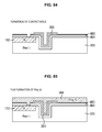
- FIG. 94 is an operation explanatory diagram with respect to a unit pixel according to a reference example.
- FIG. 95 is a schematic view illustrating an example of adopting a charge accumulation portion according to an embodiment of the present disclosure, in a unit pixel of a solid-state image sensor adopting a rolling shutter function;
- FIG. 96 is a cross-sectional view illustrating an example adopting a charge accumulation portion according to an embodiment of the present disclosure, in a unit pixel of a solid-state image sensor adopting a rolling shutter function;
- FIG. 97 is a block diagram illustrating a configuration example of electronic apparatus according to an embodiment of the present disclosure, such as an imaging device.
- FIG. 1 is a system configuration view illustrating a configuration outline of a solid-state imaging device to which the present disclosure is applied, such as a CMOS image sensor which is a kind of a solid-state imaging device of an X-Y addressing scheme.
- the CMOS image sensor denotes an image sensor created by applying CMOS process or using part of it.
- a CMOS image sensor 10 has a configuration including a pixel array portion 11 formed on a semiconductor substrate (i.e. chip) (not illustrated) and peripheral circuit portions collected on the same semiconductor substrate as that of the pixel array portion 11 .
- the peripheral circuit portions include, for example, a vertical drive portion 12 , a column processing portion 13 , a horizontal drive portion 14 and a system control portion 15 .
- the CMOS image sensor 10 further includes a signal processing portion 18 and a data storage portion 19 .
- the signal processing portion 18 and the data storage portion 19 may be mounted on the same substrate as that of the CMOS image sensor 10 or arranged on a different substrate from that of the CMOS image sensor 10 .
- each processing in the signal processing portion 18 and the data storage portion 19 may be performed by software or an external signal processing portion set on a different substrate from that of the CMOS image sensor 10 , such as a DSP (Digital Signal Processor) circuit.
- DSP Digital Signal Processor
- the pixel array portion 11 has a configuration in which unit pixels (which may be simply referred to as “pixels” below) each having a photoelectric conversion portion that generates and accumulates light charges based on a quantity of received light are arranged in a two-dimensional manner in the row and column directions, i.e. in a matrix manner.
- the row direction denotes the pixel arrangement direction of pixel rows (i.e. horizontal direction)
- the column direction denotes the pixel arrangement direction of pixel columns (i.e. vertical direction).
- a specific circuit configuration and pixel configuration of the unit pixel will be described later.
- a pixel drive wire 16 is wired along the row direction every pixel row and a vertical signal wire 17 is wired along the column direction every pixel column, in the matrix pixel arrangement.
- the pixel drive wire 16 transmits a drive signal that performs driving at the time of reading a signal from a pixel.
- FIG. 1 illustrates the pixel drive wire 16 as one wire, it is not limited to one wire.
- One end of the pixel drive wire 16 is connected to the output terminal corresponding to each row of the vertical drive portion 12 .
- the vertical drive portion 12 is configured with a shift register, an address decoder and so on, and drives all pixels of the pixel array portion 11 at the same time or drives the pixels of the pixel array portion 11 in a row unit. That is, the vertical drive portion 12 and the system control portion 15 to control the vertical drive portion 12 form a drive portion to drive each pixel of the pixel array portion 11 . Although illustration of a specific configuration of this vertical drive portion 12 is omitted, it generally has a configuration including two scanning systems of a reading scanning system and a sweeping scanning system.
- the reading scanning system selectively and sequentially scans unit pixels of the pixel array portion 11 in row units to read signals from the unit pixels.
- the signal read from the unit pixel is an analog signal.
- the sweeping scanning system performs sweeping scanning with respect to the reading rows subjected to reading scanning in the reading scanning system, earlier than the reading scanning by the time of the shutter speed.
- the electronic shutter operation denotes an operation of discarding light charges of photoelectric conversion portions and starting an exposure (i.e. starting an accumulation of light charges) anew.
- a signal read by the reading operation in the reading scanning system corresponds to the quantity of light received after the previous reading operation or electronic shutter operation. Subsequently, a period between the reading timing by the previous reading operation or the sweeping timing by the electronic shutter operation and the reading timing of the current reading operation is an exposure period of light charges in unit pixels.
- the signal output from each unit pixel of the pixel row selectively scanned by the vertical drive portion 12 is input in the column processing portion 13 via each vertical signal wire 17 every pixel column.
- the column processing portion 13 performs predetermined signal processing on the signal output from each pixel of a selected row via the vertical signal wire 17 , every pixel column of the pixel array portion 11 , and temporarily holds the pixel signal after the signal processing.
- the column processing portion 13 performs at least noise removal processing such as CDS (Correlated Double Sampling) processing.
- the CDS processing by this column processing portion 13 removes reset noise or fixed pattern noise unique to pixels such as threshold variation of amplification transistors in pixels.
- the column processing portion 13 can have an AD (analog-to-Digital) conversion function so as to convert an analog pixel signal into a digital signal and output it.
- the horizontal drive portion 14 includes a shift register, an address decoder and so on, and selects unit circuits corresponding to the pixel columns of the column processing portion 13 in order. By the selective scanning in this horizontal drive portion 14 , pixel signals subjected to signal processing every unit circuit in the column processing portion 13 are output in order.
- the system control portion 15 includes a timing generator to generate various timing signals and performs drive control of the vertical drive portion 12 , the column processing portion 13 and the horizontal drive portion 14 based on the various timings generated in the timing generator.
- the signal processing portion 18 has at least a computation processing function and performs various kinds of signal processing such as computation processing on a pixel signal output from the column processing portion 13 .
- the data storage portion 19 temporarily stores data requested in the processing.
- the CMOS image sensor 10 having the above configuration adopts a global exposure to execute the exposure start and the exposure end at the same timings with respect to all pixels in the pixel array portion 11 . That is, the collective exposure of all pixels is possible in the CMOS image sensor 10 .
- This global exposure is executed under the driving by the drive portion formed with the vertical drive portion 12 and the system control portion 15 .
- the global shutter function that realizes the global exposure is a shutter operation suitable for the case of taking an image of a subject that moves at high speed or the case of the sensing use requesting synchronism in a taken image.
- the CMOS image sensor 10 to which the present disclosure is applied is not limited to the above system configuration. As other system configurations, the following system configuration can be provided.
- CMOS image sensor 10 A having a system configuration in which the data storage portion 19 is arranged after the column processing portion 13 and a pixel signal output from the column processing portion 13 is supplied to the signal processing portion 18 via the data storage portion 19 .
- CMOS image sensor 10 B having a system configuration in which the column processing portion 13 has an AD conversion function to perform AD conversion every column or columns of the pixel array portion 11 and the data storage portion 19 and the signal processing portion 18 are arranged in parallel with respect to the column processing portion 13 .
- the solid-state imaging device e.g. CMOS image sensor
- the solid-state imaging device has two charge accumulation portions of first and second charge accumulation portions in a unit pixel to maintain a larger saturated charge amount without degrading image quality of a taken image at dark situation or low illumination.
- a flush-mounted MOS capacitor is used as the first charge accumulation portion and a capacitor of a larger capacity value per unit area than that of the first charge accumulation portion is used as the second charge accumulation portion.
- the amount relationship of saturated charge amounts is set as follows. That is, regarding the first charge accumulation portion, it is preferable that the saturated charge amount be smaller than the saturated charge amount of the photoelectric conversion portion.
- the saturated charge amount of the first charge accumulation portion is made smaller than the saturated charge amount of the photoelectric conversion portion, the difference amount is compensated in the second charge accumulation portion. Therefore, a sum of the saturated charge amount of the second charge accumulation portion and the saturated charge amount of the first charge accumulation portion is requested to be equal to or larger than the saturated charge amount of the photoelectric conversion portion.
- the flush-mounted MOS capacitor is used with respect to signals at low illumination, they are less influenced by the interface state and defection, and, compared to the related art that realizes the global exposure, dark-situation characteristics are not degraded. Therefore, the image quality of taken images at low illumination is not degraded.
- CMOS image sensor having a global shutter function that fulfills performance equivalent to that of a CMOS image sensor without the global function of the identical unit pixel size.
- CMOS image sensor in which the dynamic range is largely expanded.
- a capacitor with an area of 1 ⁇ m 2 is formed.
- the capacity value per unit area of the first charge accumulation portion is 1 fF/ ⁇ m 2
- the capacity value per unit area of the second charge accumulation portion is 10 fF/ ⁇ m 2
- the overall capacitor with an area of 1 ⁇ m 2 is formed by the first charge accumulation portion
- the capacity value of the capacitor with an area of 1 ⁇ m 2 is 1 fF.
- the capacity value of the capacitor with an area of 1 ⁇ m 2 is 7.75 fF, which is 7.75 times larger than that in a case where it is not replaced.
- the capacity value per unit area of the second charge accumulation portion is 20 fF/ ⁇ m 2
- the capacity value of the capacitor with an area of 1 ⁇ m 2 is 10.5 fF, which is 10.5 times larger than that in a case where it is not replaced.
- the degradation of dark-situation characteristics such as a dark current and white spot becomes significant. Therefore, when light charges are transferred from the photoelectric conversion portion to all pixels at the same time, light charges at low luminance are accumulated in the first charge accumulation portion.
- the “light charges at low luminance” mean light charges equal to or smaller than the saturated charge amount of the first charge accumulation portion. Since the first charge accumulation portion is formed with the flush-mounted capacitor, it is less influenced by the interface state and defection and therefore has better dark-situation characteristics than the second charge accumulation portion.
- light charges at high illumination are accumulated in both the first charge accumulation portion and the second charge accumulation portion.
- the “light charges at high illumination” means light charges over the saturated charge amount of the first charge accumulation portion.
- dark-situation characteristics such as a dark current and white spot. Therefore, even if light charges at high illumination are accumulated in the second charge accumulation portion in which there is a large leakage current, there is extremely less influence on image quality.
- a capacitor having a larger capacity value per unit area than that of the first charge accumulation portion that is, as an example of a capacitor having a larger capacity value per unit area than that of the flush-mounted MOS capacitor, there is a surface-type MOS capacitor.
- FIG. 4 illustrates a flush-mounted MOS capacitor A and a surface-side MOS capacitor B. Also, in FIG. 4A and FIG. 4B , drawing (a) illustrates the cross-sectional configuration of each MOS capacitor and drawing (b) illustrates the equivalence circuit of each MOS capacitor.
- a gate electrode 23 is arranged on a semiconductor substrate 21 through the intermediary of a gate oxide film 22 .
- the flush-mounted MOS capacitor A employs a configuration in which a charge accumulation area 24 to charge signal charges is formed in a deep part of the semiconductor substrate 21
- the surface-type MOS capacitor B employs a configuration in which a charge accumulation area 25 is formed on the substrate surface of the semiconductor substrate 21 .
- Cox represents the capacity value of the gate oxide film 22
- Cch represents the capacity value between the substrate surface and the charge accumulation area
- Csi represents the capacity value between the charge accumulation area and the substrate.
- the capacity value per unit area of the charge accumulation area 24 is Cb
- the capacity value Cb is represented by following Equation (1).
- Equation 1 is approximated by following Equation (2).
- Equation (2) Cb ⁇ Cox ⁇ 1/(1 +Cox/Cch ) ⁇ (2)
- the capacity value per unit area of the charge accumulation area is Cs
- the capacity value Cs is represented by following Equation (3).
- Cs Cox+Csi (3)
- the magnitude relationship between the capacity value Cb per unit area of the charge accumulation area 24 and the capacity value Cs per unit area of the charge accumulation area 25 is Cb ⁇ Cs, and, by embedding the charge accumulation area from the substrate surface into the substrate, the capacity value becomes small. To put it the other way around, by taking the charge accumulation area from the inside of the substrate to the substrate surface, the capacity value becomes large.
- the capacity value Cox per unit area of the gate oxide film 22 is represented by following Equation (5).
- Cox ⁇ ox/tox (5)
- ⁇ ox represents the permittivity of the gate oxide film 22 and tox represents the film thickness of the gate oxide film 22 .
- the film thickness tox of the gate oxide film 22 is important in terms of pressure resistance or leakage amount, by using a material of higher permittivity in the identical film thickness, it is possible to increase the capacity value Cox per unit area.
- the material of higher permittivity include the following materials.
- the product of the vacuum permittivity and the relative permittivity is the permittivity of each material, taking into consideration a ratio of the relative permittivity with respect to SiO 2 (relative permittivity of 3.9), it is possible to estimate an increment of the capacity value per unit area. For example, with an assumption of the surface-type MOS capacitor, when Si 3 N 4 of the same film thickness as SiO 2 is used instead, the capacity value per unit area is increased by 1.8 times, and, when Ta 2 O 5 is used, the capacity value per unit area is increased by 6.7 times.
- the combined configuration includes the configurations illustrated in FIG. 5 , that is, a configuration A combining a planar-type MOS capacitor and a junction-type capacitor, and a configuration B combining a planar-type MOS capacitor and a stack-type capacitor.
- a P-type well 52 is formed on an N-type semiconductor substrate 51 .
- An N+-type semiconductor area 41 as an intermediate electrode is formed on the surface layer part of the P-type well 52 , and the junction-type MOS capacitor is formed between the N+-type semiconductor area 41 and the P-type well 52 as a lower electrode.
- an upper electrode 42 is arranged on the substrate surface through the intermediary of an insulating film 53 , a planar-type MOS capacitor is formed in parallel with the junction-type MOS capacitor. That is, the second charge accumulation portion 40 is formed by connecting the planar-type MOS capacitor and the junction-type capacitor in parallel.
- the combined configuration B will be explained.
- the same planar-type MOS capacitor as in the case of the combined configuration A is used.
- the planar-type MOS capacitor is formed in an area separated by element isolation insulating films 55 and 56 , and, furthermore, the stack-type capacitor is formed in the upper layer by parallel connection.
- the P+-type (or N+-type) semiconductor area 43 as a lower electrode is formed on the surface layer part of the P-type well 52 and an intermediate electrode 45 is formed on the semiconductor area 43 through the intermediary of a capacity insulating film 44 .
- This configuration is a configuration of the planar-type MOS capacitor.
- the upper electrode 47 is formed on the intermediate electrode 45 through the intermediary of a capacity insulating film 46 .
- This configuration is a configuration of the stack-type capacitor.
- the intermediate electrode 45 is electrically connected to the N+-type semiconductor area 41 by a wire 57 .
- this combined configuration B that is, according to a configuration combining the planar-type MOS capacitor and the stack-type capacitor, it is possible to form a capacitor of a larger capacity value per unit area.
- FIG. 6 and FIG. 7 illustrate other configuration examples of the second charge accumulation portion 40 .
- the same reference numerals are assigned to the same components as in FIG. 5 .
- FIG. 6A is a cross-sectional view illustrating a configuration of a planar-type MOS capacitor.
- the planar MOS capacitor forming the second charge accumulation portion 40 has a configuration in which the P+-type (or N+-type) semiconductor area 43 as a lower electrode is formed on the surface layer part of the P-type well 52 and the upper electrode 45 is formed on the semiconductor area 43 through the intermediary of the capacity insulating film 44 .
- FIG. 6B is a cross-sectional view illustrating a configuration of a stack-type capacitor 1 .
- the stack-type capacitor 1 forming the second charge accumulation portion 40 has a configuration in which a lower electrode 45 is formed on the element isolation insulating film 55 and the upper electrode 47 is formed on the lower electrode 45 through the intermediary of the capacity insulating film 46 .
- FIG. 7A is a cross-sectional view illustrating a configuration of a stack-type capacitor 2 .
- the stack-type capacitor 2 forming the second charge accumulation portion 40 has a configuration in which the lower electrode 45 having a U-shaped cross-sectional surface is electrically connected to the N+-type semiconductor area 41 and the upper electrode 47 is inserted in this lower electrode 45 through the intermediary of the capacity insulating film 46 .
- the stack-type capacitor 2 In the case of this configuration of the stack-type capacitor 2 , a source voltage is applied to the upper electrode 47 or the upper electrode 47 is earthed.
- the stack-type capacitor 2 including the lower electrode 45 having a U-shaped cross-sectional surface and the upper electrode 47 embedded in the lower electrode 45 there is an advantage that it is possible to maintain a larger facing area contributing to a capacitance than a normal stack-type capacitor such as the stack-type capacitor 1 .
- FIG. 7B is a cross-sectional view illustrating a configuration of a trench-type capacitor.
- the trench-type capacitor forming the second charge accumulation portion 40 has a configuration in which a trench 48 that penetrates the P-type well 52 and reaches the substrate 51 is formed and a capacitor is formed in this trench 48 .
- the N+-type (or P+-type) semiconductor area 43 as a lower electrode is formed in the inner wall of the trench 48 , the inner wall of the semiconductor are 43 is covered with the capacity insulating film 44 and the upper electrode 45 is embedded through the intermediary of the capacity insulating film 44 .
- the second charge accumulation portion 40 is formed with a planar-type MOS capacitor, junction-type capacitor, stack-type capacitor or trench-type capacitor alone or a combination of these in which part or all of the capacity insulating film is formed with a material of a higher permittivity than that of the silicon oxide film.
- the material of a higher permittivity than that of the silicon oxide film (SiO 2 ) include Si 3 N 4 , Ta 2 0 5 , HfO 2 , ZrO 2 , and so on.
- the configuration of the second charge accumulation portion 40 is not limited to the configuration example, and, in order to enhance the capacity in a memory capacitor of DRAM or the like, it is possible to employ various methods that have been developed before.
- FIG. 8 illustrates an example of a capacitor structure in which a light leakage into the first charge accumulation portion 30 and the second charge accumulation portion 40 is suppressed with respect to the capacitor structure in FIG. 5B .
- the capacitor structure in FIG. 8 differs from the capacitor structure in FIG. 5B in providing a material of the upper electrode 47 and a light blocking film 58 .
- the upper electrode 47 and the light blocking film are formed with metal films having a light blocking effect such as w (wolfram).
- the upper electrode 47 and the light blocking film 58 can be formed with metal films subjected to barrier metal such as W/TiN/Ti, Al/TiN/Ti and Cu/TaN.
- the upper electrode 47 is arranged in the closest position to the side on which light enters the unit pixel among the electrodes of the second charge accumulation portion 40 (hereinafter referred to as “incidence side”), and also functions as a light blocking film with respect to incident light in the unit pixel. Therefore, by the upper electrode 47 , a light leakage into the second charge accumulation portion 40 is suppressed and it is possible to suppress an occurrence of false signals such as smear.
- the upper electrode 47 is connected to the P+-type (or N+-type) semiconductor area 43 by a wire (not illustrated), for example, and a predetermined source voltage is applied or the upper electrode 47 is earthed.
- the light blocking film 58 is arranged in a position closer to the incidence side than the gate electrode 33 arranged in the closest position to the incidence side among the electrodes of the first charge accumulation portion 30 , so as to cover the gate electrode 33 . Therefore, by the light blocking film 58 , a light leakage into the first charge accumulation portion 30 is suppressed and it is possible to suppress an occurrence of false signals such as smear.
- the upper electrode 47 and the light blocking film 58 are separately arranged in the unit pixel and not requested to be set to the same potential. Therefore, the freedom degree of arrangement of the upper electrode 47 and the light blocking film 58 is high, which simplifies layout design.
- the light blocking film 58 may be formed so as to overlap not only the gate electrode SG but also part of the upper portion of the adjacent gate electrode CG.
- the upper electrode 47 may be formed so as to cover up to the side surface of the intermediate electrode 45 . By this means, it is possible to further suppress a light leakage into the second charge accumulation portion 40 .
- the light blocking film 58 may be formed so as to cover up to the side surfaces of the gate electrode SG and the gate electrode CG. By this means, it is possible to further suppress a light leakage into the first charge accumulation portion 30 .
- FIG. 11 illustrates a capacitor structure example in which a leakage current from the second charge accumulation portion 40 is suppressed with respect to the capacitor structure in FIG. 8 (or FIG. 5B ).
- the capacitor structure in FIG. 11 differs from the capacitor structure in FIG. 8 in that the upper electrode 47 and the light blocking film 58 have a two-layer structure.
- a first layer 47 A adjacent to the capacity insulating film 46 of the upper electrode 47 is formed with a metal film having a higher work function (WF) and lower blocking effect than a second layer 47 B.
- the second layer 47 B is formed with a metal film having a lower work function and higher blocking effect than the first layer 47 A.
- the first layer 47 A is formed with TiN and the second layer 47 B is formed with W.
- FIG. 12 illustrates a measurement result example of EOT (Equivalent Oxide Thickness)-Jg characteristics at the time of changing the materials of the electrode 801 and the capacity insulating film 802 the capacitor structure illustrated in FIG. 13 .
- EOT Equivalent Oxide Thickness
- a characteristic 111 in FIG. 12 indicates an EOT-Jg characteristic in a case where the electrode 801 is formed with a metal film of W and the capacity insulating film 802 is formed with a NO (Nitric Oxide) film.
- a characteristic 112 indicates an EOT-Jg characteristic in a case where the electrode 801 is formed with a metal film of W and the capacity insulating film 802 formed with a High-k (high electric permittivity gate insulating film).
- a characteristic 113 indicates an EOT-jg characteristic in a case where, as illustrated in FIG. 13 , similar to the upper electrode 47 in FIG. 11 , the electrode 801 is formed with a metal film having a two-layer structure of TiN and W and the capacity insulating film 802 is formed with High-k.
- FIG. 14 illustrates potential views between the electrode 801 and a silicon substrate in the case of forming the electrode 801 in the one-layer structure of W and forming the electrode 10 in the two-layer structure of TiN and W.
- the left side illustrates a potential view in the case of forming the electrode 801 in the one-layer structure of W and the right side illustrates a potential view in the case of forming the electrode 10 in the two-layer structure of TiN and W.
- this example is provided using H f O 2 as the capacity insulating film 802 .
- the thickness of the first layer 47 A is determined taking into account the trade-off between the leakage current and the light leakage quantity, and set to, for example, 2 to 50 nm.
- the light blocking film 58 is formed with a first layer 58 A of TiN and a second layer 58 B of W.
- the light blocking film 58 is not requested to be formed in the second-layer structure.
- the upper electrode 47 and the light blocking film 58 may be formed in the two-layer structure.
- the upper electrode 47 and the light blocking film 58 may be formed in the two-layer structure.
- FIG. 17 illustrates data acquired by measuring the metal film transmittance of each material with respect to light with a wavelength of 700 nm, as a reference.
- the horizontal axis represents a film thickness (using nm as a unit) and the vertical axis represents the transmittance (using dB as a unit).
- the first layer 47 A and the second layer 47 B of the upper electrode 47 As described above, regarding materials used for the first layer 47 A and the second layer 47 B of the upper electrode 47 , based on the transmittance data and work function data as illustrated in FIG. 17 , it is preferable to form the first layer 47 A with a metal film having a higher work function and lower blocking effect than the second layer 47 B.
- an element isolation formation process is performed.
- the element isolation insulating films 55 and 56 are formed in the semiconductor substrate (i.e. P-type well 52 ).
- a sacrificial oxidation process is performed.
- a sacrificial oxide film 201 is formed on a surface of the P-type well 52 .
- an ion implant (or ion implantation (I/I)) process before the gate formation is performed.
- a two-layer semiconductor area formed with an N-type semiconductor area 31 and P-type semiconductor area 32 is formed on the surface of the P-type well 52 .
- the N+-type semiconductor area 43 is formed on the surface of the P-type well 52 .
- a gate oxidation process is performed.
- the sacrificial oxide film 201 is removed from the surface of the P-type well 52 and the capacity insulating film 44 and the insulating film 53 are formed.
- a gate electrode formation (or deposition) process is performed.
- a silicon film 202 to form the gate electrode 33 and the intermediate electrode 45 is formed.
- a gate electrode formation (or etching) process is performed.
- the silicon film 202 is processed by etching and the gate electrode 33 and the intermediate electrode 45 are formed.
- the ion implantation (I/I) process after the gate formation is performed.
- the N+-type semiconductor area 41 is formed on the surface layer part of the P-type well 52 .
- an insulating film formation (or deposition) process is performed.
- an insulating film 203 to form the capacity insulating film 46 .
- the insulating film 203 is formed with, for example, High-k.
- a light blocking film formation (or deposition) process is performed.
- a light blocking film 204 to form the upper electrode 47 and the light blocking film 58 is formed.
- the light blocking film 58 is formed with a metal film having a light blocking effect such as W, or metal films subjected to barrier metal such as W/TiN/Ti, Al/TiN/Ti and Cu/TaN.
- W a light blocking effect
- barrier metal such as W/TiN/Ti, Al/TiN/Ti and Cu/TaN.
- a light blocking film formation n (or etching) process is performed.
- the insulating film 203 and the light blocking film 204 are processed by etching and the capacity insulating film 46 , the upper electrode 47 and the light blocking film 58 are formed.
- an interlayer insulating film formation (or deposition) process is performed.
- an interlayer insulating film 205 is formed.
- a wire layer formation process is performed.
- a wire such as a wire 57 is formed.
- the wire 57 is formed with, for example, Cu, Al or W.
- the first charge accumulation portion 30 and the second charge accumulation portion 40 are formed.
- FIG. 30 is a circuit view illustrating a circuit configuration of the unit pixel 60 A to which the present disclosure is applied.
- the unit pixel 60 A has, for example, a p-n junction photodiode 61 as a photoelectric conversion portion that receives light and generates and accumulates light charges.
- the photodiode 61 generates and accumulates light charges based on a quantity of received light.
- the unit pixel 60 A includes a first transfer gate portion 62 , a second transfer gate portion 63 , a third transfer gate portion 64 , a reset gate portion 65 , a first charge accumulation portion 66 and a second charge accumulation portion 67 , an amplification transistor 68 , a selection transistor 69 and a charge ejection gate portion 70 .
- the first and second charge accumulation portions 66 and 67 correspond to the first and second charge accumulation portions described above. That is, in a circuit of the first charge accumulation portion 66 , a flush-mounted MOS capacitor is set between the first transfer gate portion 62 and the second transfer gate portion 63 .
- a drive signal SG (which may be referred to as “transfer signal SG” below) is applied to a gate electrode of the first charge accumulation portion 66 .
- the second charge accumulation portion 67 is formed with a capacitor of a larger capacity value per unit area than that of the first charge accumulation portion 66 .
- the layouts and cross-sectional surface configurations of the first and second charge accumulation portions 66 and 67 will be described later in detail.
- a plurality of drive wires are wired every pixel row, for example, as the pixel drive wire 16 in FIG. 1 .
- various drive signals TG, SG, FG, CG, RST, SEL and PG are supplied. Since each transistor is an NMOS transistor in the above configuration, these drive signals TG SG, FG, CG, RST, SEL and PG are pulse signals in which the high-level (for example, source voltage V DD ) state is an active state and the low-level state (for example, negative potential) is an inactive state.
- the drive signal TG is applied to a gate electrode of the first transfer gate portion 62 as a transfer signal.
- the first transfer gate portion 62 is connected between the photodiode 61 and the first charge accumulation portion 66 .
- the drive signal TG (which may be referred to as “transfer signal TG” below) gets in an active state, in response to this, the first transfer gate portion 62 gets in a conduction state.
- transfer signal TG which may be referred to as “transfer signal TG” below
- the drive signal FG is applied to a gate electrode of the second transfer gate portion 63 as a transfer signal.
- the second transfer gate portion 63 is connected between the first charge accumulation portion 66 and a floating diffusion portion (hereinafter referred to as “FD portion”) 71 to which a gate electrode of the amplification transistor 68 is connected.
- the FD portion 71 converts light charges into electric signals such as voltage signals and outputs these.
- the drive signal FG (which may be referred to as “transfer signal FG” below) gets in an active state, in response to this, the second transfer gate portion 63 gets in a conduction state. By this means, the light charges accumulated in the first charge accumulation portion 66 are transferred to the FD portion 71 .
- the drive signal CG is applied to a gate electrode of the third transfer gate portion 64 as a transfer signal.
- the third transfer gate portion 64 is connected between the first charge accumulation portion 66 and the second charge accumulation portion 67 .
- the drive signal CG (which may be referred to as “transfer signal CG” below) gets in an active state, in response to this, the third transfer gate portion 64 gets in a conduction state.
- the drive signal RST is applied to a gate electrode of the reset gate portion 65 as a reset signal.
- one source/drain area is connected to the reset voltage V DR and the other source/drain area is connected to the FD portion 71 .
- the drive signal RST (which may be referred to as “reset signal RST” below) gets in an active state, in response to this, the reset gate portion 65 gets in a conduction state. By this means, the potential of the FD portion 71 is reset to the level of the reset voltage V DR .
- the gate electrode is connected to the FD portion 71 and the drain electrode is connected to the source voltage V DD , so as to be an input portion of a reading circuit which reads light charges acquired by the photoelectric conversion in the photodiode 61 and which is a so-called source follower circuit. That is, in the amplification transistor 68 , the source electrode is connected to the vertical signal wire 17 via the selection transistor 69 such that the amplification transistor 68 and a constant current source 80 connected to one end of the vertical signal wire 17 form a source follower circuit.
- the drive signal SEL is applied to a gate electrode of the selection transistor 69 as a selection signal.
- the selection transistor 69 is connected between the source electrode of the amplification transistor 68 and the vertical signal wire 17 .
- the drive signal SEL (which may be referred to as “selection signal SEL” below) gets in an active state, in response to this, the selection transistor 69 gets in a conduction state.
- the drive signal PG is applied to a gate electrode of the charge ejection gate portion 70 as a charge ejection control signal.
- the charge ejection gate portion 70 is connected between the photodiode 61 and a charge ejection portion (for example, source voltage V DD ).
- the drive signal PG (which may be referred to as “charge ejection control signal PG” below) gets in an active state, in response to this, the charge ejection gate portion 70 gets in a conduction state.
- a predetermined amount of light charges defined in advance from the photodiode 61 or all light charges accumulated in the photodiode 61 are selectively ejected to the charge ejection portion.
- the charge ejection gate portion 70 is provided for the following purpose. By making the charge ejection gate portion 70 get in a conduction state in a period in which light charges are not accumulated, it is possible to prevent charges over the saturated charge amount of the photodiode 61 from overflowing into the first charge accumulation portion 66 , the second charge accumulation portion 66 and peripheral pixels.
- FIG. 31 is a schematic view illustrating a pixel configuration of the unit pixel 60 A, and, in the figure, the same reference numerals are assigned to the same components as in FIG. 30 . Also, FIG. 31 illustrates a plane pattern illustrating a pixel layout and an A-A′ arrow cross-sectional surface and B-B′ arrow cross-sectional surface in the plane pattern.
- the photodiode (PD) 61 has a PN-junction diode configuration in which an N-type semiconductor area 611 is formed in the P-type well 52 on the semiconductor substrate 51 .
- a P-type semiconductor area 612 is formed on the surface layer part of this photodiode 61 , so as to be a flush-mounted photodiode in which the depletion end is separated from an interface (so-called HAD (Hole Accumulation Diode) sensor configuration).
- HAD Hole Accumulation Diode
- the first transfer gate portion 62 includes a gate electrode 621 arranged on the substrate surface through the intermediary of a gate insulating film (not illustrated) and has a configuration in which a P-type semiconductor area 622 is formed on the substrate surface layer part. Compared to a case where the P-type semiconductor area 622 is not formed, this semiconductor area 622 slightly deepens the potential below the gate electrode 621 . By this means, as clear from the B-B′ arrow cross-sectional view, the P-type semiconductor area 622 forms an overflow path to transfer light charges equal to or larger than a predetermined amount overflown from the photodiode 61 , specifically, light charges over the saturated charge amount of the photodiode 61 to the first charge accumulation portion 66 .
- the first charge accumulation portion 66 includes a gate electrode 661 arranged on the substrate surface through the intermediary of a gate insulating film (not illustrated) and is formed below the gate electrode 661 as a flush-mounted MOS capacitor. That is, the first charge accumulation portion 66 is formed with a flush-type MOS capacitor including: the N-type semiconductor area 662 formed in the P-type well 52 below the gate electrode 661 ; and the P-type semiconductor 663 formed on the surface layer part of the N-type semiconductor area 662 .
- the second transfer gate portion 63 includes a gate electrode 631 arranged on the substrate surface through the intermediary of a gate insulating film (not illustrated).
- the N-type semiconductor area 662 of the first charge accumulation portion 66 is one source/drain area and an N+-type semiconductor area 711 as the FD portion 71 is the other source/drain area.
- the unit pixel 60 A has a pixel configuration in which the first charge accumulation portion 66 is formed as the flush-mounted MOS capacitor below the gate electrode 661 formed adjacent to the first and second transfer gate portions 62 and 63 .
- the third transfer gate portion 64 includes a gate electrode 641 arranged on the substrate surface through the intermediary of a gate insulating film (not illustrated).
- the N-type semiconductor area 662 of the first charge accumulation portion 66 is one source/drain area and an N+-type semiconductor area 642 formed on the substrate surface layer part is the other source/drain area.
- One end of the second charge accumulation portion 67 is electrically connected to the N+-type semiconductor area 642 of the third transfer gate portion 64 .
- the other end of the second charge accumulation portion 67 is connected to the negative-side power source (for example, ground).
- the second transfer gate portion 63 , the gate electrode 661 of the first charge accumulation portion 66 and the third transfer gate portion 64 have operations to combine or divide the potentials of the FD portion 71 , the first charge accumulation portion 66 and the second charge accumulation portion 67 .
- the third transfer gate portion 64 has a configuration in which the N-type semiconductor area 643 is formed on the surface layer part of a channel portion. Compared to a case where the N-type semiconductor area 643 is not formed, this semiconductor area 643 slightly deepens the potential below the gate electrode 641 . By this means, as clear from the A-A′ arrow cross-sectional view, the N-type semiconductor area 643 forms an overflow path to transfer light charges over the saturated charge amount of the first charge accumulation portion 66 to the second charge accumulation portion 67 .
- the overflow paths formed below the first and third transfer gate portions 62 and 64 are formed such that light charges accumulated in the first charge accumulation portion 66 are transferred to the second charge accumulation portion 67 without being leaked in the photodiode 61 .
- the unit pixel 60 A by providing the overflow path below the gate electrode 641 of the third transfer gate portion 64 , it is possible to accumulate light charges overflown from the photodiode 61 at high illumination even in the second charge accumulation portion 67 .
- the third transfer gate portion 64 even when the third transfer gate portion 64 is in a non-conduction state, it is possible to transfer light charges equal to or larger than a predetermined amount, which are overflown from the first charge accumulation portion 66 , to the second charge accumulation portion 67 and accumulate the light charges in the second charge accumulation portion 67 .
- circuit operations of the unit pixel 60 A will be explained.
- FIG. 32 illustrates the timing chart of the selection signal SEL, the reset signal RST, the transfer signal TG, the charge ejection control signal PG, the transfer signal CG the transfer signal SG and the transfer signal FG of the unit pixel 60 A.
- FIG. 33 to FIG. 40 illustrate potential states of the unit pixel 60 A in the N-th row at times ta to th in the timing chart of FIG. 32 .
- the charge ejection control signal PG is in an active state, while the selection signal SEL, the reset signal RST, the transfer signal CG the transfer signal SG and the transfer signal FG get in an active state in all pixels at the same time.
- the selection transistor 69 , the reset gate portion 65 , the third transfer gate portion 64 , the gate electrode 661 of the first charge accumulation portion 66 , the second transfer gate portion 63 and the charge ejection gate portion 70 get in a conduction state.
- FIG. 33 illustrates a potential state of the unit pixel 60 A at time to between time t 1 and time t 2 .
- the potentials of the FD portion 71 , the first charge accumulation portion 66 and the second charge accumulation portion 67 are combined and the combined area is reset.
- FIG. 34 illustrates a potential state of the unit pixel 60 A at time tb between time t 2 and t 3 .
- the transfer signal TG and the transfer signal SG get in an active state and the first transfer gate portion 62 and the gate electrode 661 of the first charge accumulation portion 66 get in a conduction state.
- FIG. 35 illustrates a potential state of the unit pixel 60 A at time tc between time t 3 and time t 4 .
- the light charges accumulated in the photodiode 61 are transferred to the first charge accumulation portion 66 and accumulated in the first charge accumulation portion 66 .
- the transfer signal TG gets in an inactive state in all pixels at the same time while the charge ejection control signal PG gets in an active state. Also, while the first transfer gate portion 62 gets in a non-conduction state, the charge ejection gate portion 70 gets in a conduction state. By this means, the exposure period common in all pixels is finished.
- the transfer signal SG gets in an inactive state
- the gate electrode 661 of the first charge accumulation portion 66 gets in a non-conduction state and the potential of the first charge accumulation portion 66 returns to the original.
- the accumulation charge amount of the first charge accumulation portion 66 is over the saturated charge amount
- light charges overflown from the first charge accumulation portion 66 are transferred to the second charge accumulation portion 67 via the overflow path of the third transfer gate portion 64 .
- the selection signal SEL in the N-th row gets in an active state
- the selection transistor 69 in the N-th row gets in a conduction state and therefore the unit pixel 60 A in the N-th row gets in a selection state.
- the reset signal RST gets in an active state
- the reset gate portion 65 gets in a conduction state and therefore the FD portion 71 is reset.
- the reset signal RST gets in an inactive state.
- FIG. 36 illustrates a potential state of the unit pixel 60 A at time td between time t 6 and time t 7 .
- the potential of the FD portion 71 in this state is output as first reset level N 1 to the vertical signal wire 17 through the amplification transistor 68 and the selection transistor 69 .
- FIG. 37 illustrates a potential state of the unit pixel 60 A at time to between time t 7 and time t 8 .
- light charges accumulated in the first charge accumulation portion 66 are transferred to the FD portion 71 .
- the transfer signal FG gets in an inactive state and the second transfer gate portion 63 gets in a non-conduction state.
- FIG. 38 illustrates a potential state of the unit pixel 60 A at time tf between time t 8 and time t 9 .
- the potential of the FD portion 71 in this state is output to the vertical signal wire 17 through the amplification transistor 68 and the selection transistor 69 .
- the transfer signals CG SG and FG get in an active state at the same time and the third transfer gate portion 64 , the gate electrode 661 of the first charge accumulation portion 66 and the second transfer gate portion 63 get in a conduction state.
- FIG. 39 illustrates a potential state of the unit pixel 60 A at time tg between time t 9 and time t 10 .
- the potentials of the FD portion 71 , the first charge accumulation portion 66 and the second charge accumulation portion 67 are combined and light charges are accumulated in the overall combined area. Also, these light charges are output as a second signal level S 2 to the vertical signal wire 17 through the amplification transistor 68 and the selection transistor 69 .
- the reset signal RST gets in an active state and the reset gate portion 65 gets in a conduction state.
- the area combining the potentials of the FD portion 71 , the first charge accumulation portion 66 and the second charge accumulation portion 67 is reset.
- the reset signal gets in an active state and the reset gate portion 65 gets in a non-conduction state.
- FIG. 40 illustrates a potential state of the unit pixel 60 A at time th between time t 11 and time t 12 .
- the potential of the area combining the potentials in this state is output as a second reset level N 2 to the vertical signal wire 17 through the amplification transistor 68 and the selection transistor 69 .
- the selection signal SEL in the N-th row gets in an inactive state
- the selection transistor 69 in the N-th row gets in a non-conduction state and therefore the unit pixel 60 A in the N-th row gets in a non-selection state.
- the transfer signal FG the transfer signal SG and the transfer signal CG are caused to get in an inactive state in this order, and the second transfer gate portion 63 , the gate electrode 661 of the first charge accumulation portion 66 and the third transfer gate portion 64 are caused to get in a non-conduction state.
- the transfer signal FG, the transfer signal SG and the transfer signal CG are caused to get in an inactive state in this order, such that, when the gate electrode 661 of the first charge accumulation portion 66 is in a conduction state, channel charges accumulated in the substrate surface are accumulated in the second charge accumulation portion 67 .
- the reset is not performed only by the second charge accumulation portion 67 , and therefore there is no concern that an offset is caused in pixel signals by the reset of the channel charges.
- the first reset level N 1 , the first signal level S 1 , the second signal level S 2 and the second reset level N 2 are sequentially output from the unit pixel 60 A to the vertical signal wire 17 .
- the first reset level N 1 , the first signal level S 1 , the second signal level S 2 and the second reset level N 2 sequentially output in this way are subjected to predetermined signal processing in a signal processing portion in a subsequent stage. The signal processing will be described later in detail.
- the unit pixel 60 A by using the flush-mounted MOS capacitor as the first charge accumulation portion 66 and the capacitor of a larger capacity value per unit area than that of the first charge accumulation portion 66 as the second charge accumulation portion 67 , it is possible to maintain a larger saturated charge amount. By contrast, in a case where the equivalent saturated charge amount is acceptable, it is possible to reduce the unit pixel size by the saved space.
- FIG. 41 is a circuit view illustrating a circuit configuration of the unit pixel 60 A 1 according to variation example 1 of the unit pixel 60 A, and, in the figure, the same reference numerals are assigned to the same components as in FIG. 30 .
- the unit pixel 60 A 1 according to this variation example 1 differs from the unit pixel 60 A in that the charge ejection gate portion 70 is omitted.
- FIG. 42 is a circuit view illustrating a circuit configuration of the unit pixel 60 A 2 according to variation example 2 of the unit pixel 60 A, and, in the figure, the same reference numerals are assigned to the same components as in FIG. 30 .
- the unit pixel 60 A 2 according to this variation example 2 differs from the unit pixel 60 A in that the selection transistor 69 is omitted. Also, in the unit pixel 60 A 2 , a function of pixel selection by the selection transistor 69 is realized by varying the drain voltage DRN applied to the drain electrode of the reset gate portion 65 .
- the amplification transistor 68 gets in an activation state to perform signal output operations. That is, the amplification transistor 68 operates as a selection transistor in cooperation with a switching operation of the drain voltage DRN. By omitting the selection transistor 69 , there is an advantage that it is possible to reduce one circuit element forming the unit pixel 60 every pixel.
- FIG. 43 is a timing chart illustrating each signal state.
- the circuit operations and the circuit operations of the unit pixel 60 A are different only in the timing of the reset signal RST and are basically the same.
- circuit elements forming a pixel can be shared between a plurality of pixels.
- FIG. 44 is a circuit view illustrating a circuit configuration according to specific example 1 of the pixel share.
- it provides an example case where part of pixel configuration elements is shared between four adjacent pixels 60 A- 1 to 60 A- 4 .
- the number of sharing pixels is not limited to 4 pixels.
- the sharing may be performed in four pixels of two pixels in the row direction and two pixels in the column direction or in four pixels in the column direction.
- Specific example 1 provides a pixel share example in the case of the pixel configuration of the unit pixel 60 A. Also, circuit elements including the reset gate portion 65 after the FD portion 71 , that is, three circuit elements of the reset gate portion 65 , the amplification transistor 68 and the selection transistor 69 are shared between four pixels.
- FIG. 45 is a circuit view illustrating a circuit configuration according to specific example 2 of pixel share. Similar to the above, an example case is provided where part of pixel configuration elements is shared between four adjacent pixels 60 A- 1 to 60 A- 4 . However, the number of sharing pixels is not limited to four pixels. Also, as relationships between the four adjacent pixels 60 A- 1 to 60 A- 4 , for example, the sharing may be performed in four pixels of two pixels in the row direction and two pixels in the column direction or in four pixels in the column direction.
- Specific example 2 provides a pixel share example in the case of the pixel configuration of the unit pixel 60 A 2 according to variation example 2. Also, circuit elements including the reset gate portion 65 after the FD portion 71 , that is, two circuit elements of the reset gate portion 65 and the amplification transistor 68 are shared between four pixels.
- FIG. 46 is a potential view in the substrate depth direction provided for explaining requirements to perform pinning of the substrate surface and combine the potentials of the FD portion 71 , the first charge accumulation portion 66 and the second charge accumulation portion 67 .
- the potentials of the first to third transfer gate portions 62 to 64 and the gate electrode 661 of the first charge accumulation portion 66 in a non-conduction state regardless of a conductive layer immediately below a gate oxide film, they are set to a potential (for example, negative potential) to make the substrate surface get in a pinning state.
- a potential for example, negative potential
- the substrate surface potentials of the second and third transfer gate portions 63 and 64 and the gate electrode 661 of the first charge accumulation portion 66 in a conduction state are set to a potential higher than the reset voltage V DR , that is, a potential applied to the drain of the reset gate portion 65 .
- V DR reset voltage
- FIG. 47 illustrates a variation example of a pixel configuration of a unit pixel of a plane pattern illustrating a pixel layout of the unit pixel 60 A described with reference to FIG. 9 .
- the same reference numerals are assigned to the components corresponding to those in FIG. 9 .
- the plane pattern of the unit pixel 60 A in FIG. 47 and the plane pattern of the unit pixel 60 A in FIG. 9 are substantially the same but are largely different in that a position of the second charge accumulation portion (Cap) 67 is illustrated.
- FIG. 48 and FIG. 49 are schematic views illustrating configuration examples of the second charge accumulation portion 67 A.
- FIG. 48 illustrates an A-A′ arrow cross-sectional surface in the plane pattern of the unit pixel 60 A in FIG. 47 and a B-B′ arrow cross-sectional surface in the C part of the A-A arrow cross-sectional view.
- illustration of the N-type semiconductor substrate 51 in FIG. 5 and a part corresponding to the insulating film is omitted.
- FIG. 49 illustrates a plane view of the periphery of the second charge accumulation portion 67 A.
- an N-type semiconductor area 102 As illustrated in FIG. 48 , an N-type semiconductor area 102 , a P-type semiconductor area 103 having a U-shaped cross-sectional surface and an N-type semiconductor area 104 are formed on the surface layer part of a P-type semiconductor area 101 corresponding to the P-type well 52 in FIG. 5 . Also, an element isolation insulating film 105 is formed on the concave part of the P-type semiconductor area 103 . Also, one of the N-type semiconductor area 102 and the N-type semiconductor area 104 is connected to a power source and the other is connected to a ground.
- An intermediate electrode 111 including polysilicon is formed, as an accumulation node, above the N-type semiconductor area 104 as a lower electrode through the intermediary of a capacity insulating film (not illustrated).
- the intermediate electrode 111 is electrically connected to the N-type semiconductor area 102 by wires 121 to 123 .
- a planar-type MOS capacitor (hereinafter referred to as “first capacitor”) is formed between the intermediate electrode 111 and the N-type semiconductor area 104 .
- the wire 121 and the wire 123 have a three-layer structure of W (Wolfram), TiN (Titanium Nitride) and Ti (Titanium).
- the TiN layer is a barrier layer and the Ti layer is a contact layer.
- an upper layer wire 122 has a three-layer structure of Cu (Cuprum), TaN (Tantalum Nitride) and Ta (Tantalum).
- the TaN layer is a barrier layer and the Ta layer is a contact layer.
- An upper electrode 112 is formed above the intermediate electrode 111 through the intermediary of a capacity insulating film (not illustrated) so as to cover part of the upper and side surfaces of the intermediate electrode 111 .
- the upper electrode 112 is connected to the N-type semiconductor area 104 by wires 124 to 126 .
- a stack-type capacitor (hereinafter referred to as “second capacitor”) is formed between the intermediate electrode 111 and the upper electrode 112 so as to be connected to the first capacitor in parallel.
- the second charge accumulation portion 67 A is formed with these first capacitor and second capacitor.
- the upper electrode 112 for example, wolfram is used, which is used as a light blocking material in an image sensor such as a CCD (Charge Coupled Device) image sensor and has a high extinction coefficient and high optical absorption.
- the wires 121 and 123 similar to the wires 121 and 123 , the wires 124 and 126 have a three-layer structure of W, TiN and Ti, for example.
- an upper layer wire 125 has a three-layer structure of Cu, TaN and Ta, for example.
- the second charge accumulation portion 67 A as illustrated in FIG. 48 and FIG. 49 , there is an exposed part, which is not covered by the upper electrode 112 having a light blocking effect, in the upper and side surfaces of the intermediate electrode 111 , as seen from the top. Therefore, for example, light enters the intermediate electrode 111 from an interspace in an area A 1 in FIG. 48 and charges are generated by photoelectric conversion, which is an occurrence cause of false signals (or false images).
- contacts i.e. junction parts
- materials of largely different work functions are joined.
- an electric field is generated by work function differences in the contacts C 1 to C 4 , and, by this electric field, electrons are likely to be excited from the defect level of the junction parts or their periphery, which is an occurrence cause of dark current.
- the contact C 5 represents a contact between the upper layer wire 125 and the wire 124
- the contact C 6 represents a contact between the upper layer wire 125 and the wire 126 , where these are different-type junction parts.
- FIG. 50 and FIG. 51 are schematic views illustrating configuration examples of the second charge accumulation portion 67 B.
- the second charge accumulation portion 67 B suppresses a false signal and dark current caused in the second charge accumulation portion 67 A described above.
- FIG. 50 illustrates an A-A′ arrow cross-sectional surface in the plane pattern of the unit pixel 60 A in FIG. 47 and a B-B′ arrow cross-sectional surface in the C part of the A-A′ arrow cross-sectional view.
- illustration of the N-type semiconductor substrate 51 in FIG. 5 and a part corresponding to the insulating film is omitted.
- FIG. 51 illustrates a plane view of the periphery of the second charge accumulation portion 67 B.
- the same reference numerals are assigned to the components corresponding to those in FIG. 48 or FIG. 49 .
- an intermediate electrode 151 including polysilicon is formed, as an accumulation node, above the N-type semiconductor area 104 as a lower electrode through the intermediary of a capacity insulating film (not illustrated).
- a connection portion 151 A is formed in the intermediate electrode 151 and is directly connected to the N-type semiconductor area 102 in an electrical manner.
- a planar-type MOS capacitor (hereinafter referred to as “first capacitor”) is formed between the intermediate electrode 151 and the N-type semiconductor area 104 .
- An upper electrode 152 is formed above the intermediate electrode 151 through the intermediary of a capacity insulating film (not illustrated) so as to cover the entire upper and side surfaces of the intermediate electrode 151 .
- the upper electrode 152 is connected to the N-type semiconductor area 104 by the wires 124 to 126 .
- a stack-type capacitor (hereinafter referred to as “second capacitor”) is formed between the intermediate electrode 151 and the upper electrode 152 so as to be connected to the first capacitor in parallel.
- the second charge accumulation portion 67 B is formed with these first capacitor and second capacitor.
- wolfram having a high extinction coefficient is used for the upper electrode 152 .
- other metal materials can be used as long as they unite light-blocking performance and performance as the upper electrode of the second capacitor.
- wolfram as the upper electrode 112 , with a thickness of around 200 nm, it is possible to dim light by around ⁇ 100 dB.
- the upper and side surfaces of the intermediate electrode 151 are covered by the upper electrode 152 having a light blocking effect and incident light into the intermediate electrode 151 is blocked. Therefore, an occurrence of false signals (or false images) by photoelectric conversion in the intermediate electrode 151 is suppressed.
- the intermediate electrode 151 is formed with polysilicon of the same type as the N-type semiconductor area 102 (i.e. silicon substrate) and directly connected to the N-type semiconductor area 102 .
- the contact C 11 having a small work function difference is present as a contact between the N-type semiconductor area 102 and the intermediate electrode 151 , and therefore it is possible to remove different-type material junction parts. As a result, a field occurrence by work function differences is reduced and an occurrence of dark current is suppressed.
- the intermediate electrode 151 in addition to polysilicon, it is possible to use a material which is lattice-matched to silicon and has a small work function difference with respect to the silicon.
- the compound of polysilicon chalcopyrite, zinc sulfur and gallium phosphide can be used for the intermediate electrode 151 .
- a result of forming silicon by epitaxial growth so as to be lattice-matched to the N-type semiconductor area 102 can be used for the intermediate electrode 151 .
- FIG. 52 and FIG. 53 are schematic views illustrating configuration examples of the second charge accumulation portion 67 C.
- the second charge accumulation portion 67 C and the second charge accumulation portion 67 B are compared, there is a difference that the intermediate electrode has a two-layer configuration.
- FIG. 52 illustrates an A-A′ arrow cross-sectional surface in the plane pattern of the unit pixel 60 A in FIG. 29 and a B-B′ arrow cross-sectional surface in the C part of the A-A′ arrow cross-sectional view.
- FIG. 52 illustration of the N-type semiconductor substrate 51 in FIG. 5 and a part corresponding to the insulating film is omitted.
- FIG. 53 illustrates a plane view of the periphery of the second charge accumulation portion 67 C.
- the same reference numerals are assigned to the components corresponding to those in FIG. 50 or FIG. 51 .
- an intermediate electrode 181 including polysilicon is formed, as an accumulation node, above the N-type semiconductor area 104 as a lower electrode through the intermediary of a capacity insulating film (not illustrated). Also, a planar-type MOS capacitor (hereinafter referred to as first capacitor) is formed between the intermediate electrode 181 and the N-type semiconductor area 104 .
- An intermediate electrode 182 including polysilicon is formed, as an accumulation node, above the intermediate electrode 181 so as to partially overlap the intermediate electrode 181 , seen from the above.
- a connection portion 182 A is formed in the intermediate electrode 182 and directly connected to the N-type semiconductor area 102 in an electrical manner.
- a connection portion 182 B is formed in the intermediate electrode 182 and directly connected to the intermediate electrode 181 in an electrical manner.
- An upper electrode 183 is formed above the intermediate electrodes 181 and 182 through the intermediary of a capacity insulating film (not illustrated) so as to cover the entire upper and side surfaces of the intermediate electrodes 181 and 182 .
- the upper electrode 183 is connected to the N-type semiconductor area 104 by the wires 124 to 126 .
- a stack-type capacitor (hereinafter referred to as second capacitor) is formed between the intermediate electrode 182 and the upper electrode 183 so as to be connected to the first capacitor in parallel.
- the second charge accumulation portion 67 C is formed with these first capacitor and second capacitor.
- the upper electrode 183 it is possible to use the same material as that of the upper electrode 152 of the second charge accumulation portion 67 B.
- the upper and side surfaces of the intermediate electrodes 181 and 182 are covered by the upper electrode 183 having a light blocking effect and incident light into the intermediate electrodes 181 and 182 is blocked. Therefore, an occurrence of false signals (or false images) by photoelectric conversion in the intermediate electrodes 181 and 182 is suppressed.
- the intermediate electrode 182 is formed with polysilicon of the same type as the N-type semiconductor area 102 (i.e. silicon substrate) and directly connected to the N-type semiconductor area 102 .
- the intermediate electrode 181 is formed with polysilicon of the same type as the N-type semiconductor area 102 (i.e. silicon substrate) and directly connected to the N-type semiconductor area 102 .
- the intermediate electrode has a two-layer configuration such that, compared to the intermediate electrode 151 of the second charge accumulation portion 67 B, the intermediate electrode 182 is formed in a higher position.
- intermediate electrodes 181 and 182 similar to the intermediate electrode 151 if the second charge accumulation portion 67 B, in addition to polysilicon, it is possible to use a material which is lattice-matched to silicon and has a small work function difference with respect to the silicon.
- FIG. 54 and FIG. 55 are schematic views illustrating configuration examples of the second charge accumulation portion 67 D.
- the second charge accumulation portion 67 D and the second charge accumulation portion 67 B are compared, there is a difference that the upper electrode is directly connected to the N-type semiconductor area 104 .
- FIG. 54 illustrates an A-A′ arrow cross-sectional surface in the plane pattern of the unit pixel 60 A in FIG. 47 and a B-B′ arrow cross-sectional surface in the C part of the A-A′ arrow cross-sectional view.
- illustration of the N-type semiconductor substrate 51 in FIG. 5 and a part corresponding to the insulating film is omitted.
- FIG. 55 illustrates a plane view of the periphery of the second charge accumulation portion 67 D.
- the same reference numerals are assigned to the components corresponding to those in FIG. 50 or FIG. 51 .
- an upper electrode 211 is formed above the intermediate electrode 151 through the intermediary of a capacity insulating film (not illustrated) so as to cover the entire upper and side surfaces of the intermediate electrode 151 .
- a connection portion 211 A is formed in the upper electrode 211 and directly connected to the N-type semiconductor area 104 in an electrical manner.
- a stack-type capacitor (hereinafter referred to as second capacitor) is formed between the intermediate electrode 151 and the upper electrode 211 so as to be connected in parallel to the first capacitor between the intermediate electrode 151 and the N-type semiconductor area 104 .
- the second charge accumulation portion 67 D is formed with these first capacitor and second capacitor.
- the upper electrode 211 for example, it is possible to use the same material as that of the upper electrode 152 of the second charge accumulation portion 67 B. However, for example, in a case where the upper electrode 152 is formed with wolfram, a three-layer structure of W, TiN and Ti is employed in at least the vicinity of the contact C 31 with respect to the N-type semiconductor area 104 .
- the second charge accumulation portion 67 D similar to the second charge accumulation portion 67 B, it is possible to suppress an occurrence of false signals (or false images) by photoelectric conversion in the intermediate electrode 151 and an occurrence of dark current in the junction part C 11 between the N-type semiconductor area 102 and the intermediate electrode 151 .
- FIG. 56 is a schematic view illustrating a configuration example of the second charge accumulation portion 67 E.
- the second charge accumulation portion 67 E and the second charge accumulation portion 67 D are compared, there is a difference that a metal material is used for the intermediate electrode instead of polysilicon.
- FIG. 56 illustrates an A-A′ arrow cross-sectional surface in the plane pattern of the unit pixel 60 A in FIG. 47 and a B-B′ arrow cross-sectional surface in the C part of the A-A′ arrow cross-sectional view.
- the same reference numerals are assigned to the components corresponding to those in FIG. 54 .
- the intermediate electrode 241 has a similar shape to the intermediate electrode 151 of the second charge accumulation portion 67 D but differs from the intermediate electrode 151 in that it is formed with a metal material such as titanium and wolfram. Also, in a case where the intermediate electrode 241 is formed with wolfram, as illustrated in FIG. 57 , a three-layer structure of W, TiN and Ti is employed at least in the vicinity of the contact C 41 with respect to the N-type semiconductor area 102 .
- the intermediate electrode 241 even if a metal material is used for the intermediate electrode 241 , compared to the second charge accumulation portion 67 A, it is possible to reduce the number of different-type material junction parts between the intermediate electrode 241 and the N-type semiconductor area 102 . Therefore, in the second charge accumulation portion 67 E, compared to the second charge accumulation portion 67 A, it is possible to suppress an occurrence of dark current in different-type junction parts.
- FIG. 58 is a schematic view illustrating a configuration example of the second charge accumulation portion 67 F.
- the second charge accumulation portion 67 F is formed with a cylinder-type capacitor.
- FIG. 58 illustrates an A-A′ arrow cross-sectional surface in the plane pattern of the unit pixel 60 A in FIG. 47 .
- the same reference numerals are assigned to the components corresponding to those in FIG. 48 .
- a T-shaped lower electrode 271 including polysilicon is formed on the N-type semiconductor area 102 as an accumulation node so as to be directly connected to the N-type semiconductor area 102 in an electrical manner.
- An upper electrode 272 is formed above the lower electrode 271 through the intermediary of a capacity insulating film (not illustrated) so as to cover the entire upper surface of the lower electrode 271 and substantially the entire side surface of the lower electrode 271 .
- the upper electrode 272 is connected to an upper layer wire 282 by a wire 281 .
- the upper electrode 152 is set to a predetermined potential.
- a cylinder-type capacitor is formed between the lower electrode 271 and the upper electrode 272 .
- the second charge accumulation portion 67 F is formed with this cylinder-type capacitor.
- the gate electrode 641 is connected to the upper layer wire 284 via the wire 283 .
- the wires 281 and 283 have a three-layer structure of W, TiN and Ti.
- the upper layer wire 282 and the upper layer wire 284 have a three-layer structure of Cu, TaN and Ta.
- the entire upper side surface of the lower electrode 271 and substantially the entire side of the lower electrode 271 are covered by the upper electrode 272 having a light blocking effect and incident light into the lower electrode 271 is blocked. Therefore, an occurrence of false signals (or false images) by photoelectric conversion in the lower electrode 271 is suppressed.
- the lower electrode 271 is formed with polysilicon of the same type as the N-type semiconductor area 102 (i.e. silicon substrate) and directly connected to the N-type semiconductor area 102 . Accordingly, only a contact C 51 having a small work function difference is present as a contact between the N-type semiconductor area 102 and the lower electrode 271 , and therefore it is possible to remove different-type material conjunction portions. As a result, a field occurrence by work function differences is reduced and an occurrence of dark current is suppressed.
- the lower electrode 271 similar to the intermediate electrode 151 of the second charge accumulation portion 67 B, in addition to polysilicon, it is possible to use a material which is lattice-matched to silicon and has a small work function difference with respect to the silicon.
- the lower electrode 271 similar to the intermediate electrode 241 of the second charge accumulation portion 67 E, it is possible to use a metal material such as titanium and wolfram. In this case, although the work function difference in the contact C 51 is large, compared to the second charge accumulation portion 67 A, it is possible to reduce the number of different-type material conjunction parts and suppress an occurrence of dark current.
- FIG. 59 is a schematic view illustrating a configuration example of the second charge accumulation portion 67 G.
- the second charge accumulation portion 67 G is formed with a trench-type capacitor.
- FIG. 59 illustrates an A-A′ arrow cross-sectional surface in the plane pattern of the unit pixel 60 A in FIG. 47 .
- the same reference numerals are assigned to the components corresponding to those in FIG. 48 .
- a trench is formed in the P-type semiconductor area 101 and a trench-type lower electrode 301 is formed in the trench through the intermediary of a capacity insulating film (not illustrated).
- the lower electrode 301 it is desirable to use a material having a higher light blocking effect, and, for example, a material having a high extinction coefficient such as wolfram and aluminum is used. Also, it is possible to use other metal materials or alloy of multiple materials.
- an intermediate electrode 302 including polysilicon is formed as an accumulation node through the intermediary of a capacity insulating film (not illustrated). Also, the intermediate electrode 302 is directly connected to the N-type semiconductor area 102 in an electrical manner. Subsequently, the first capacitor is formed between the intermediate electrode 302 and the lower electrode 301 .
- An upper electrode 303 is formed above the intermediate electrode 302 through the intermediary of a capacity insulating film (not illustrated) so as to cover the entire upper surface of the intermediate electrode 302 and substantially the entire side surface of the intermediate electrode 302 .
- the upper electrode 303 is directly connected to the lower electrode 301 in an electrical manner.
- the second capacitor is formed between the intermediate electrode 302 and the upper electrode 303 so as to be connected to the first capacitor in parallel.
- the second charge accumulation portion 67 G is formed with these first capacitor and second capacitor.
- the upper electrode 303 for example, it is possible to use the same material as that of the lower electrode 301 .
- the lower electrode 301 and the upper electrode 303 have a three-layer structure of W, TiN and Ti.
- the entire upper surface of the intermediate electrode 302 and substantially the entire side surface of the intermediate electrode 302 are covered by those lower electrode 301 and upper electrode 303 having a light blocking effect, and incident light into the intermediate electrode 302 is blocked. Therefore, an occurrence of false signals (or false images) by photoelectric conversion in the intermediate electrode 302 is suppressed.
- the intermediate electrode 302 is formed with polysilicon of the same type as the N-type semiconductor area 102 (i.e. silicon substrate) and directly connected to the N-type semiconductor area 102 .
- the intermediate electrode 302 is formed with polysilicon of the same type as the N-type semiconductor area 102 (i.e. silicon substrate) and directly connected to the N-type semiconductor area 102 .
- the intermediate electrode 302 similar to the intermediate electrode 151 of the second charge accumulation portion 67 B, in addition to polysilicon, it is possible to use a material which is lattice-matched to silicon and has a small work function difference with respect to the silicon.
- the intermediate electrode 302 similar to the intermediate electrode 241 of the second charge accumulation portion 67 E, it is possible to use a metal material such as titanium and wolfram. In this case, although the work function difference in the contact C 61 is large, compared to the second charge accumulation portion 67 A, it is possible to reduce the number of different-type material conjunction parts and suppress an occurrence of dark current.
- the second charge accumulation portion 67 G to a unit pixel of a back-illuminated solid-state image sensor, it is possible to block incident light into the intermediate electrode 302 by the lower electrode 301 or the like and suppress an occurrence of false signals (or false images).
- the second charge accumulation portions 67 A to 67 E and the second charge accumulation portion 67 G are formed with two capacitors of the first capacitor and the second capacitor, it is possible to form them with one of two capacitors.
- an electrode connected to the N-type semiconductor area 102 may be formed with a material which is lattice-matched to a material of the semiconductor substrate and has a small work function difference with respect to this material.
- the P-type semiconductor area 101 is formed on the semiconductor substrate including silicon, and the N-type semiconductor area 102 and the N-type semiconductor area 104 are formed by injecting N-type impurities into the P-type semiconductor area 101 . Also, a trench is formed and P-type impurities are injected in a gap between the N-type semiconductor area 102 and the N-type semiconductor area 104 to form an element isolation including the P-type semiconductor area 103 and the element isolation insulating film 105 .
- an insulating film 401 by an oxide film is formed on the surface of the semiconductor substrate.
- patterning by lithography method is performed to remove the insulating film 401 and form a contact hole to connect the N-type semiconductor area 102 and the intermediate electrode 151 .
- a medical solution such as DHF (Dilute Hydrofluoric Acid) instead of a dry etching method, it is possible to mitigate damage to the semiconductor substrate and suppress an occurrence of defection. As a result, it is possible to reduce an occurrence of dark current.
- polysilicon 402 used for the intermediate electrode 151 is formed. At this time, through the contact hole, the polysilicon 402 is joined to the N-type semiconductor area 102 .
- the intermediate electrode 151 is formed.
- the intermediate electrode 151 instead of the polysilicon 402 , by forming a material having a small work function difference with respect to silicon by lattice-matching to the silicon or forming silicon by epitaxial growth, it is possible to form the intermediate electrode 151 .
- a capacity insulating film 403 is formed.
- the surface of the intermediate electrode 151 is covered with the capacity insulating film 403 .
- the capacity insulating film 403 when a material of a higher permittivity is used, there is an advantage in maintaining the capacity per unit area.
- wolfram 406 used for the upper electrode 152 is formed.
- the upper electrode 152 is formed.
- the insulating film 401 and the capacity insulating film 403 are removed and a contact hole is formed to connect the N-type semiconductor area 104 and the wire 126 .
- wires 153 to 155 are formed and the N-type semiconductor area 104 and the upper electrode 152 are electrically connected.
- the second charge accumulation portion 67 B is formed.
- an insulating film 431 is formed on the surface of the semiconductor substrate.
- a material of the insulating film 431 anything is possible as long as it can insulate between the lower electrode 271 and the semiconductor substrate, for example, SiO 2 or SiN is used.
- the insulating film 43 is removed by the dry etching method or wet etching method, and a contact hole to connect the N-type semiconductor area 102 and the lower electrode 271 is formed.
- polysilicon 432 used for the lower electrode 271 and the gate electrode 641 is formed. At this time, through a contact hole, the polysilicon 432 is jointed to the N-type semiconductor area 102 .
- the lower electrode 271 instead of the polysilicon 432 , by forming a material having a small work function difference with respect to silicon by lattice-matching to the silicon or forming silicon by epitaxial growth, it is possible to form the lower electrode 271 .
- the lower electrode 271 by forming a metal material such as titanium and wolfram.
- a capacity insulating film 433 is formed.
- the entire surface of the lower electrode 271 is formed with the capacity insulating film 433 .
- a high-permittivity film such as SiN, SiO 2 , HfO 2 and ZrO is used.
- wolfram 434 used for the upper electrode 272 is formed on the capacity insulating film 433 .
- an interlayer insulating film 435 is formed between the unit pixel 60 A and the upper layer wires 282 and 284 .
- the interlayer insulating film 435 for example, SiO 2 is used.
- the interlayer insulating film 435 is planarized by a CMP (Chemical Medical polishing) method.
- CMP Chemical Medical polishing
- the upper layer wires 282 and 284 having a three-layer structure of Cu, TaN and Ta are formed so as to be connected to the wires 281 and 283 , respectively.
- the second charge accumulation portion 67 F is formed.
- a trench is formed in the P-type semiconductor area 101 of the substrate semiconductor.
- this trench is formed by forming an insulating film on the semiconductor substrate, performing patterning of the film by the lithography method and removing it by the dry etching method.
- an insulating film 461 to insulate the semiconductor substrate and the lower electrode 301 is formed.
- the insulating film 46 may be formed by thermal oxidation of silicon on the surface of the semiconductor substrate.
- wolfram 462 used for the lower electrode 301 is formed on the insulating film 461 . Also, as described above, instead of the wolfram 462 , it is possible to form another metal material or alloy of multiple materials to form the lower electrode 301 .
- a capacity insulating film 463 is formed.
- the surface of the lower electrode 301 is covered with the capacity insulating film 463 .
- a material such as SiN and High-k is used for the capacity insulating film 463 .
- the insulating film 461 and the capacity insulating film 463 are removed by the lithography method and the dry etching method or wet etching method, and a contact hole to connect the intermediate electrode 302 and the N-type semiconductor area 102 is formed.
- polysilicon 464 used for the intermediate electrode 302 is formed. At this time, through the contact hole, the polysilicon 464 is jointed to the N-type semiconductor area 102 .
- the intermediate electrode 302 instead of the polysilicon 464 , by forming a material having a small work function difference with respect to silicon by lattice-matching to the silicon or forming silicon by epitaxial growth, it is possible to form the intermediate electrode 302 .
- the intermediate electrode 302 by forming a metal material such as titanium and wolfram.
- a capacity insulating film 465 is formed.
- the entire surface of the intermediate electrode 302 is covered with the capacity insulating film 465 .
- the capacity insulating film 463 and the capacity insulating film 465 are removed by the lithography method and the dry etching method to form a contact hole to connect the lower electrode 301 and the upper electrode 303 .
- the second charge accumulation portion 67 G is formed.
- signals are output to the vertical signal wire 17 in the order from the first reset level N 1 , the first signal level S 1 , the second signal level S 2 to the second reset level N 2 .
- the first reset level N 1 , the first signal level S 1 , the second signal level S 2 and the second reset level N 2 are subjected to predetermined noise removal processing and signal processing.
- the noise removal processing in the column processing portion 13 and computation processing in the signal processing portion 18 will be explained.
- FIG. 90 illustrates a timing diagram provided for explaining noise removal processing in the cases of processing examples 1 and 2 in the column processing portion 13 .
- a difference is found between the a voltage signal S 1 based on light charges transferred to the FD portion 71 at the time of signal reading and a voltage signal N 1 based on a reset level before the light charges are transferred to the FD portion 71 . Further, a difference is found between a voltage signal S 2 based on light charges accumulated in the FD portion 71 , the first charge accumulation portion 66 and the second charge accumulation portion 67 , and a voltage signal N 2 based on a reset level after the second charge accumulation portion 67 is reset.
- SN 1 S 1 ⁇ N 1
- SN 2 S 2 ⁇ N 2 are established.
- the signals S 1 and N 1 output earlier are subjected to CDS processing to remove a reset noise and a fixed-pattern noise unique to a pixel such as threshold variation of the amplification transistor in the pixel.
- the signals S 2 and N 2 output later are subjected to CDS processing in which, although a fixed-pattern noise unique to a pixel such as threshold variation of the amplification transistor in the pixel is removed, a reset noise is not removed.
- CDS processing it denotes computation processing without using a frame memory, and therefore there are advantages that it is possible to simplify the circuit configuration and realize a low cost.
- processing example 2 a storage section such as a frame memory is requested to use information of the previous frame. Therefore, it follows that, for example, the computation processing in processing example 2 uses the data storage portion 19 as a storage section in the signal processing portion 18 or uses a frame memory in an external DSP circuit.
- a difference is found between the voltage signal S 1 based on light charges transferred to the FD portion 71 at the time of signal reading and the voltage signal N 1 based on a reset level before the light charges are transferred to the FD portion 71 .
- a difference is found between the voltage signal S 2 based on light charges accumulated in the FD portion 71 , the first charge accumulation portion 66 and the second charge accumulation portion 67 , and a voltage signal N 2 A in the previous frame.
- This voltage signal N 2 A denotes a signal based on a reset level after light charges accumulated in the FD portion 71 , the first charge accumulation portion 66 and the second charge accumulation portion 67 in the previous frame are reset.
- processing example 2 even the signals S 2 and N 2 output later are subjected to CDS processing to remove a reset noise and a fixed-pattern noise unique to a pixel such as threshold variation of the amplification transistor in the pixel.
- a storage section such as a frame memory
- the first difference is referred to as SN 1
- the second difference is referred to as SN 2
- the gain is referred to as G
- the computation value of the second difference SN 2 is referred to as SN 2 ′
- SN ⁇ ⁇ 2 ′ G ⁇ SN ⁇ ⁇ 2 ( 7 )
- Cfd represents the capacity value of the FD portion 71
- Cgs represents the capacity value of the first charge accumulation portion 66
- Ccap represents the capacity value of the second charge accumulation portion 67 .
- the gain G is equivalent to the capacity ratio.
- FIG. 91 illustrates relationships between the incident amount and the first difference SN 1 , the second difference SN 2 and the computation value SN 2 ′ of the second difference SN 2 .
- a predetermined threshold Vt set in advance is used.
- the predetermined threshold Vt is set in advance in an area in which the first difference SN 1 is not saturated in the photoresponse property and the photoresponse property is linear.
- a value of the first difference SN 1 within a predetermined range and the computation value SN 2 ′ of the second difference SN 2 are synthesized at a ratio set in advance and output as the pixel signal SN.
- the predetermined threshold Vt denotes a value set in advance in an area in which the first difference SN 1 is not saturated in the photoresponse property and the photoresponse property is linear.
- a main feature of the above-described embodiments is that there are two charge accumulation portions 66 and 67 in a unit pixel and the second charge accumulation portion 67 is formed with a capacitor having a larger capacity value per unit area than that of the first charge accumulation portion 66 .
- the capacity value per unit area is equivalent between the two charge accumulation portions 66 and 67 , it is possible to expand the dynamic range. This will be explained with reference to FIG. 93 .
- the second transfer gate portion 63 is caused to get in a conduction state such that light charges equal to or larger than a predetermined amount overflown from the photodiode 61 are ejected.
- the exposure period in the photodiode 61 is referred to as Tpd and the period to accumulate the light charges overflown from the photodiode 61 in the second charge accumulation portion 67 is referred to as Tcap.
- the unit pixel is operated in the timing chart illustrated in FIG. 93 to restrict the exposure time Tcap in the second charge accumulation portion 67 . By this operation, it is possible to compress information on the high illumination side and, even if the capacity value of the second charge accumulation portion 67 is small or equivalent to that of the first charge accumulation portion 66 , it is possible to expand the dynamic range.
- the FD portion 71 is temporarily reset once and the light charges, which are accumulated in the second charge accumulation portion 67 and overflown from the photodiode 61 , are read as signals on the high illumination side. Unlike other embodiments, the signals on the high illumination side to temporarily reset the FD portion 71 do not include light charges accumulated in the first charge accumulation portion 66 .
- a voltage signal based on light charges transferred to the FD portion 71 is referred to as S 1
- a voltage signal based on a reset level before the light charges are transferred to the FD portion 71 is referred to as N 1
- the first difference is referred to as SN 1
- S 3 a voltage signal based on light charges accumulated in the FD portion 71 , the first charge accumulation portion 66 and the second charge accumulation portion 67 in a case where the FD portion 71 is reset immediately before the reading.
- a voltage signal of the reset levels or reset suitability levels of the FD portion 71 , the first charge accumulation portion 66 and the second charge accumulation portion 67 is referred to as N 2
- a third difference is referred to as SN 3
- a gain is referred to as G
- a computation value of the third difference SN 3 is referred to as SN 3 ′. Subsequently, the following computation is possible.
- the pixel signal SN is output as follows.
- a feature of the present embodiment lies in that light charges overflown from the photodiode 61 at high illumination are accumulated in the photodiode 61 and further in the first and second charge accumulation portions 66 and 67 .
- the configuration of the second charge accumulation portion 67 described with reference to FIG. 47 to FIG. 59 is applicable to a unit pixel different from the above unit pixels.
- a rear-surface-type solid-state image sensor such as a rear-surface-type CIS (Contact Image Sensor).
- FIG. 95 is a schematic view illustrating a pixel configuration in a case where a unit pixel 500 of a solid-state image sensor adopting a rolling shutter function includes a charge accumulation portion (Cap) 501 having the same configuration as that of the second charge accumulation portion 67 .
- Cap charge accumulation portion
- FIG. 96 is a schematic view illustrating a configuration example of the charge accumulation portion 501 .
- this figure illustrates an example where the same configuration as that of the second charge accumulation portion 67 B in FIG. 50 is applied to the charge accumulation portion 501 , other configurations described above are equally applicable.
- the present disclosure is not limitedly applied to the CMOS image sensor. That is, the present disclosure is applicable to all solid-state imaging devices of an X-Y address scheme in which unit pixels are two-dimensionally arranged in a matrix manner.
- the present disclosure is not limitedly applied to a solid-state imaging device that detects distribution of incident-light quantities of visible light and photographs it as an image, and is applicable to all solid-state imaging devices that photograph distribution of incident-light quantities of infrared ray, X-ray or grain as an image.
- the solid-state imaging device may be formed as one chip or formed in a module format including an imaging function collectively packaging an imaging portion and a signal processing portion or optical unit.
- all pixels in the present disclosure denote all pixels of parts present in an image, and dummy pixels are excluded. Also, in the present disclosure, if the time difference or image distortion is sufficiently small to the extent that a problem does not arise, it is possible to perform scanning at high speed every multiple rows (for example, several dozens of rows) instead of operations in all pixels at the same time. Further, in the present disclosure, it is possible to apply a global shutter operation to not only all pixels present in an image but also to multiple predetermined rows.
- the conduction types of a device configuration in the unit pixel described above is just an example, and the N type and the P type may be reverse. Also, there is a case where the magnitude relationship of electrical potentials or potentials of the above portions is reverse depending on whether a majority carrier moving in a unit pixel is a positive hole or an electron.
- the present disclosure is not limitedly applied to a solid-state imaging device but is applicable to the overall electronic apparatuses using a solid-state imaging device as an image taking portion (i.e. photoelectric conversion portion), such as: an imaging device including a digital still camera and video camera; a portable terminal device having an imaging function such as a portable telephone machine; and a copy machine using a solid-state imaging device as an image reading portion.
- a solid-state imaging device as an image taking portion
- an imaging device including a digital still camera and video camera such as a portable terminal device having an imaging function such as a portable telephone machine
- a copy machine using a solid-state imaging device as an image reading portion.
- the above module format mounted in an electronic apparatus that is, a camera module may be provided in an imaging device.
- FIG. 97 is a block diagram illustrating a configuration example of an electronic apparatus according to the present disclosure, such as an imaging device.
- an imaging device 300 has an optical unit including a lens group 301 , and an image sensor (or imaging device) 302 , a DSP circuit 303 , a frame memory 304 , a display device 305 , a recording device 306 , an operation unit 307 and a power source unit 308 . Subsequently, the DSP circuit 303 , the frame memory 304 , the display device 305 , the recording device 306 , the operation unit 307 and the power source unit 308 are mutually connected via a bus line 309 .
- the lens group 301 imports incident light (or image light) from a subject and forms an image on the imaging surface of the image sensor 302 .
- incident light or image light
- the light quantity of incident light formed on the imaging surface by the lens group 301 is converted into electric signals in a unit pixel and output as pixel signals.
- the display device 305 includes a panel-type display device such as a liquid crystal display device and an organic EL (Electro Luminescence) display device, and displays a motion picture or still picture taken in the image sensor 302 .
- the recording device 306 records the motion picture or still picture taken in the image sensor 302 , in a storage medium such as a videotape and a DVD (Digital Versatile Disk).
- the operation unit 307 issues operation instructions with respect to various functions held in the imaging device under user's operations.
- the power source unit 308 adequately supplies various powers corresponding to operation powers of the DSP circuit 303 , the frame memory 304 , the display device 305 , the recording device 306 and the operation unit 307 to these supply targets.
- the imaging device of the above configuration as an imaging device including a video camera, a digital still camera and a camera module for mobile devices such as a portable telephone machine.
- a solid-state imaging device such as the CMOS image sensor 10 according to the above embodiment, it is possible to provide the following operational effects.
- the CMOS image sensor 10 can realize an imaging without distortion by global exposure. Therefore, it can be realized as an imaging device suitable for the case of taking an image of a subject that moves at high speed, in which image distortion is not acceptable, or the case of the sensing use requesting synchronism in a taken image.
- the CMOS image sensor 10 can maintain a larger saturated charge amount without degrading image quality of a taken image at dark situation or low illumination, in other words, it is possible to increase a capacity value to accumulate light charges. Also, when it is possible to maintain a larger saturated charge amount, if an equivalent saturated charge amount is requested, it is possible to decrease the unit pixel size by the maintained saturated charge amount and realize many pixels according thereto. Therefore, it is possible to realize high quality of taken images.
- a pixel configuration for example, an overflow path or a conduction layer of a surface layer portion of a flush-mounted MOS capacitor is not limited, and various changes are possible in circuit views and timing charts without departing from the scope of the present technology.
Landscapes
- Engineering & Computer Science (AREA)
- Physics & Mathematics (AREA)
- Power Engineering (AREA)
- Condensed Matter Physics & Semiconductors (AREA)
- Electromagnetism (AREA)
- General Physics & Mathematics (AREA)
- Computer Hardware Design (AREA)
- Microelectronics & Electronic Packaging (AREA)
- Multimedia (AREA)
- Signal Processing (AREA)
- Solid State Image Pick-Up Elements (AREA)
- Transforming Light Signals Into Electric Signals (AREA)
Applications Claiming Priority (4)
| Application Number | Priority Date | Filing Date | Title |
|---|---|---|---|
| JP2012-020867 | 2012-02-02 | ||
| JP2012020867A JP5970834B2 (ja) | 2012-02-02 | 2012-02-02 | 固体撮像装置、固体撮像装置の製造方法、及び、電子機器 |
| JP2012-022724 | 2012-02-06 | ||
| JP2012022724A JP6007499B2 (ja) | 2012-02-06 | 2012-02-06 | 固体撮像装置、固体撮像装置の製造方法、及び、電子機器 |
Publications (2)
| Publication Number | Publication Date |
|---|---|
| US20130200479A1 US20130200479A1 (en) | 2013-08-08 |
| US9490373B2 true US9490373B2 (en) | 2016-11-08 |
Family
ID=48902184
Family Applications (1)
| Application Number | Title | Priority Date | Filing Date |
|---|---|---|---|
| US13/749,393 Active 2033-04-16 US9490373B2 (en) | 2012-02-02 | 2013-01-24 | Solid-state imaging device and electronic apparatus with improved storage portion |
Country Status (2)
| Country | Link |
|---|---|
| US (1) | US9490373B2 (zh) |
| CN (2) | CN103247642B (zh) |
Cited By (3)
| Publication number | Priority date | Publication date | Assignee | Title |
|---|---|---|---|---|
| US20160307947A1 (en) * | 2015-04-16 | 2016-10-20 | Caeleste Cvba | Pixel with Increased Charge Storage |
| US11665452B2 (en) | 2019-06-05 | 2023-05-30 | Samsung Electronics Co., Ltd. | Image sensor |
| US11908876B2 (en) | 2014-06-09 | 2024-02-20 | Semiconductor Energy Laboratory Co., Ltd. | Semiconductor device including photoelectric conversion element |
Families Citing this family (23)
| Publication number | Priority date | Publication date | Assignee | Title |
|---|---|---|---|---|
| JP6167338B2 (ja) * | 2013-10-15 | 2017-07-26 | 株式会社Joled | 有機el表示装置の製造方法および検査装置 |
| FR3013546B1 (fr) * | 2013-11-15 | 2017-05-19 | Trixell | Mise en commun de deux colonnes de pixels d'un detecteur d'images |
| JP5968350B2 (ja) | 2014-03-14 | 2016-08-10 | キヤノン株式会社 | 撮像装置、および、撮像システム |
| JP6376785B2 (ja) * | 2014-03-14 | 2018-08-22 | キヤノン株式会社 | 撮像装置、および、撮像システム |
| JP2016063156A (ja) * | 2014-09-19 | 2016-04-25 | 株式会社東芝 | 撮像素子及び固体撮像装置 |
| JP2016063165A (ja) * | 2014-09-19 | 2016-04-25 | 株式会社東芝 | 撮像素子及び固体撮像装置 |
| WO2016136486A1 (ja) | 2015-02-27 | 2016-09-01 | ソニー株式会社 | 固体撮像装置及び電子機器 |
| WO2017130728A1 (ja) * | 2016-01-29 | 2017-08-03 | ソニー株式会社 | 固体撮像装置および電子機器 |
| JP6904730B2 (ja) | 2016-03-08 | 2021-07-21 | 株式会社半導体エネルギー研究所 | 撮像装置 |
| JP2017163010A (ja) | 2016-03-10 | 2017-09-14 | ソニー株式会社 | 撮像装置、電子機器 |
| CN108780803B (zh) * | 2016-03-29 | 2023-03-17 | 索尼公司 | 固态成像装置及电子设备 |
| JPWO2017169882A1 (ja) | 2016-03-31 | 2019-02-14 | ソニー株式会社 | 撮像素子、撮像素子の製造方法、及び、電子機器 |
| JP6701108B2 (ja) * | 2017-03-21 | 2020-05-27 | キヤノン株式会社 | 固体撮像装置及び撮像システム |
| JP2019080305A (ja) * | 2017-10-20 | 2019-05-23 | ソニーセミコンダクタソリューションズ株式会社 | 固体撮像素子、固体撮像素子の駆動方法および電子機器 |
| JP2019097136A (ja) | 2017-11-28 | 2019-06-20 | セイコーエプソン株式会社 | ロボット、アナログデジタル変換器、及び、固体撮像装置 |
| CN108281440B (zh) * | 2018-01-24 | 2021-04-23 | 德淮半导体有限公司 | 图像传感器及其制造方法 |
| CN110278396B (zh) * | 2018-03-16 | 2024-07-12 | 松下知识产权经营株式会社 | 摄像装置 |
| WO2019235130A1 (ja) * | 2018-06-08 | 2019-12-12 | ソニーセミコンダクタソリューションズ株式会社 | 撮像素子、積層型撮像素子及び固体撮像装置 |
| JP7356214B2 (ja) | 2018-09-04 | 2023-10-04 | キヤノン株式会社 | 撮像装置、その製造方法及びカメラ |
| KR102661820B1 (ko) * | 2019-02-11 | 2024-05-02 | 삼성전자주식회사 | 이미지 센서 및 그것의 구동 방법 |
| KR20200139327A (ko) * | 2019-06-04 | 2020-12-14 | 삼성전자주식회사 | 이미지 센싱 장치 |
| CN112151557B (zh) * | 2019-06-26 | 2024-07-02 | 格科微电子(上海)有限公司 | Cmos图像传感器的实现方法 |
| CN112738430B (zh) * | 2020-12-30 | 2023-05-26 | 长春长光辰芯微电子股份有限公司 | 可切换像素结构 |
Citations (22)
| Publication number | Priority date | Publication date | Assignee | Title |
|---|---|---|---|---|
| JPH0661449A (ja) | 1992-08-06 | 1994-03-04 | Nec Corp | 半導体装置の製造方法 |
| JPH0992801A (ja) | 1995-09-19 | 1997-04-04 | Samsung Electron Co Ltd | 半導体装置のキャパシタ形成方法 |
| JPH1079476A (ja) | 1996-08-16 | 1998-03-24 | United Microelectron Corp | 半導体記憶装置のコンデンサ構造体の製造方法 |
| JP2001250934A (ja) | 1999-12-28 | 2001-09-14 | Hynix Semiconductor Inc | キャパシタ構造を有するイメージセンサ及びその製造方法 |
| US6317154B2 (en) * | 1998-02-27 | 2001-11-13 | Intel Corporation | Method to reduce reset noise in photodiode based CMOS image sensors |
| US20020192934A1 (en) * | 2001-06-14 | 2002-12-19 | Jeong Young Soo | 2-input nor gate with NMOS transistors and PMOS transistors formed on different semiconductor layers |
| US20050063141A1 (en) * | 2003-09-19 | 2005-03-24 | Samsung Electronics Co., Ltd. | Analog capacitor having at least three high-k dielectric layers, and method of fabricating the same |
| US20050196915A1 (en) * | 2004-02-24 | 2005-09-08 | Jeong Yong-Kuk | Method of fabricating analog capacitor using post-treatment technique |
| US20060065915A1 (en) * | 2004-09-27 | 2006-03-30 | Kazunobu Kuwazawa | Sold-state imaging devices |
| JP3874135B2 (ja) | 1997-12-05 | 2007-01-31 | 株式会社ニコン | 固体撮像素子 |
| US20070063295A1 (en) * | 2005-09-20 | 2007-03-22 | Samsung Electronics Co.,Ltd. | Gate electrode, method of forming the same, transistor having the gate electrode, method of manufacturing the same, semiconductor device having the gate electrode and method of manufacturing the same |
| US20080036888A1 (en) * | 2006-08-09 | 2008-02-14 | Tohoku University | Optical sensor and solid-state imaging device |
| JP2009165186A (ja) | 2009-04-23 | 2009-07-23 | Tohoku Univ | 光センサおよび固体撮像装置 |
| US20090200454A1 (en) * | 2008-01-10 | 2009-08-13 | Stmicroelectronics S.A. | Pixel circuit for global electronic shutter |
| US20090251582A1 (en) * | 2008-04-03 | 2009-10-08 | Sony Corporation | Solid state imaging device, driving method of the solid state imaging device, and electronic equipment |
| US20090303366A1 (en) * | 2008-06-05 | 2009-12-10 | International Business Machines Corporation | Interlevel conductive light shield |
| US20100245647A1 (en) * | 2009-03-24 | 2010-09-30 | Sony Corporation | Solid-state imaging device, driving method of solid-state imaging device, and electronic apparatus |
| US20110007196A1 (en) * | 2008-05-02 | 2011-01-13 | Canon Kabushiki Kaisha | Solid-state imaging apparatus |
| US20110019038A1 (en) * | 2009-07-23 | 2011-01-27 | Sony Corporation | Solid-state imaging device, drive method therefor, and electronic device |
| CN102208426A (zh) | 2010-03-31 | 2011-10-05 | 索尼公司 | 固态摄像器件、固态摄像器件的驱动方法和电子装置 |
| JP2011199816A (ja) | 2010-02-26 | 2011-10-06 | Sony Corp | 固体撮像装置、固体撮像装置の駆動方法、及び、電子機器 |
| US9293503B2 (en) * | 2011-07-12 | 2016-03-22 | Sony Corporation | Solid-state imaging device, method for driving the same, method for manufacturing the same, and electronic device |
Family Cites Families (2)
| Publication number | Priority date | Publication date | Assignee | Title |
|---|---|---|---|---|
| US7719590B2 (en) * | 2007-03-16 | 2010-05-18 | International Business Machines Corporation | High dynamic range imaging cell with electronic shutter extensions |
| US9543356B2 (en) * | 2009-03-10 | 2017-01-10 | Globalfoundries Inc. | Pixel sensor cell including light shield |
-
2013
- 2013-01-24 US US13/749,393 patent/US9490373B2/en active Active
- 2013-01-25 CN CN201310028975.0A patent/CN103247642B/zh active Active
- 2013-01-25 CN CN201611255149.XA patent/CN106952932B/zh active Active
Patent Citations (25)
| Publication number | Priority date | Publication date | Assignee | Title |
|---|---|---|---|---|
| JPH0661449A (ja) | 1992-08-06 | 1994-03-04 | Nec Corp | 半導体装置の製造方法 |
| JPH0992801A (ja) | 1995-09-19 | 1997-04-04 | Samsung Electron Co Ltd | 半導体装置のキャパシタ形成方法 |
| JPH1079476A (ja) | 1996-08-16 | 1998-03-24 | United Microelectron Corp | 半導体記憶装置のコンデンサ構造体の製造方法 |
| JP3874135B2 (ja) | 1997-12-05 | 2007-01-31 | 株式会社ニコン | 固体撮像素子 |
| US6317154B2 (en) * | 1998-02-27 | 2001-11-13 | Intel Corporation | Method to reduce reset noise in photodiode based CMOS image sensors |
| JP2001250934A (ja) | 1999-12-28 | 2001-09-14 | Hynix Semiconductor Inc | キャパシタ構造を有するイメージセンサ及びその製造方法 |
| US20020192934A1 (en) * | 2001-06-14 | 2002-12-19 | Jeong Young Soo | 2-input nor gate with NMOS transistors and PMOS transistors formed on different semiconductor layers |
| US20050063141A1 (en) * | 2003-09-19 | 2005-03-24 | Samsung Electronics Co., Ltd. | Analog capacitor having at least three high-k dielectric layers, and method of fabricating the same |
| US20050196915A1 (en) * | 2004-02-24 | 2005-09-08 | Jeong Yong-Kuk | Method of fabricating analog capacitor using post-treatment technique |
| US20060065915A1 (en) * | 2004-09-27 | 2006-03-30 | Kazunobu Kuwazawa | Sold-state imaging devices |
| US20070063295A1 (en) * | 2005-09-20 | 2007-03-22 | Samsung Electronics Co.,Ltd. | Gate electrode, method of forming the same, transistor having the gate electrode, method of manufacturing the same, semiconductor device having the gate electrode and method of manufacturing the same |
| US20080036888A1 (en) * | 2006-08-09 | 2008-02-14 | Tohoku University | Optical sensor and solid-state imaging device |
| US20090200454A1 (en) * | 2008-01-10 | 2009-08-13 | Stmicroelectronics S.A. | Pixel circuit for global electronic shutter |
| JP2009268083A (ja) | 2008-04-03 | 2009-11-12 | Sony Corp | 固体撮像装置、固体撮像装置の駆動方法および電子機器 |
| US20090251582A1 (en) * | 2008-04-03 | 2009-10-08 | Sony Corporation | Solid state imaging device, driving method of the solid state imaging device, and electronic equipment |
| US20110007196A1 (en) * | 2008-05-02 | 2011-01-13 | Canon Kabushiki Kaisha | Solid-state imaging apparatus |
| US20090303366A1 (en) * | 2008-06-05 | 2009-12-10 | International Business Machines Corporation | Interlevel conductive light shield |
| US20100245647A1 (en) * | 2009-03-24 | 2010-09-30 | Sony Corporation | Solid-state imaging device, driving method of solid-state imaging device, and electronic apparatus |
| JP2009165186A (ja) | 2009-04-23 | 2009-07-23 | Tohoku Univ | 光センサおよび固体撮像装置 |
| US20110019038A1 (en) * | 2009-07-23 | 2011-01-27 | Sony Corporation | Solid-state imaging device, drive method therefor, and electronic device |
| JP2011199816A (ja) | 2010-02-26 | 2011-10-06 | Sony Corp | 固体撮像装置、固体撮像装置の駆動方法、及び、電子機器 |
| US8917341B2 (en) * | 2010-02-26 | 2014-12-23 | Sony Corporation | Solid-state image pickup apparatus, driving method for solid-state image pickup apparatus and electronic device |
| CN102208426A (zh) | 2010-03-31 | 2011-10-05 | 索尼公司 | 固态摄像器件、固态摄像器件的驱动方法和电子装置 |
| JP2011216970A (ja) | 2010-03-31 | 2011-10-27 | Sony Corp | 固体撮像装置、固体撮像装置の駆動方法、および、電子機器 |
| US9293503B2 (en) * | 2011-07-12 | 2016-03-22 | Sony Corporation | Solid-state imaging device, method for driving the same, method for manufacturing the same, and electronic device |
Non-Patent Citations (1)
| Title |
|---|
| Chinese Office Action issued Aug. 3, 2016 for corresponding Chinese Application No. 201310028975.0. |
Cited By (4)
| Publication number | Priority date | Publication date | Assignee | Title |
|---|---|---|---|---|
| US11908876B2 (en) | 2014-06-09 | 2024-02-20 | Semiconductor Energy Laboratory Co., Ltd. | Semiconductor device including photoelectric conversion element |
| US20160307947A1 (en) * | 2015-04-16 | 2016-10-20 | Caeleste Cvba | Pixel with Increased Charge Storage |
| US9699398B2 (en) * | 2015-04-16 | 2017-07-04 | Caeleste Cvba | Pixel with increased charge storage |
| US11665452B2 (en) | 2019-06-05 | 2023-05-30 | Samsung Electronics Co., Ltd. | Image sensor |
Also Published As
| Publication number | Publication date |
|---|---|
| CN106952932B (zh) | 2021-03-09 |
| CN103247642B (zh) | 2017-07-14 |
| CN103247642A (zh) | 2013-08-14 |
| CN106952932A (zh) | 2017-07-14 |
| US20130200479A1 (en) | 2013-08-08 |
Similar Documents
| Publication | Publication Date | Title |
|---|---|---|
| US9490373B2 (en) | Solid-state imaging device and electronic apparatus with improved storage portion | |
| JP6007499B2 (ja) | 固体撮像装置、固体撮像装置の製造方法、及び、電子機器 | |
| JP5458690B2 (ja) | 固体撮像装置およびカメラ | |
| JP5970834B2 (ja) | 固体撮像装置、固体撮像装置の製造方法、及び、電子機器 | |
| EP2942813B1 (en) | Optical sensor and solid-state imaging device | |
| US8917341B2 (en) | Solid-state image pickup apparatus, driving method for solid-state image pickup apparatus and electronic device | |
| JP5167799B2 (ja) | 固体撮像装置およびカメラ | |
| TWI505453B (zh) | 固態成像裝置,用於驅動其之方法,用於製造其之方法,及電子裝置 | |
| US11646342B2 (en) | Imaging device and electronic device | |
| US8350305B2 (en) | Solid-state imaging device and camera | |
| JP6024103B2 (ja) | 撮像素子、撮像素子の駆動方法、撮像素子の製造方法、および電子機器 | |
| US8810703B2 (en) | Solid-state image pickup device, driving method of solid-state image pickup device, and electronic device | |
| JP5335271B2 (ja) | 光電変換装置及びそれを用いた撮像システム | |
| US20130214371A1 (en) | Solid-state imaging device, image sensor, method of manufacturing image sensor, and electronic apparatus | |
| US20080036888A1 (en) | Optical sensor and solid-state imaging device | |
| JP2009165186A (ja) | 光センサおよび固体撮像装置 | |
| US20110241080A1 (en) | Solid-state imaging device, method for manufacturing the same, and electronic apparatus | |
| JP2016009777A (ja) | 固体撮像素子およびその製造方法、並びに電子機器 | |
| KR101277990B1 (ko) | 광학 센서 및 고체 촬상 장치 | |
| JP2020080377A (ja) | 固体撮像装置 | |
| CN118693118A (zh) | 摄像装置和电子设备 |
Legal Events
| Date | Code | Title | Description |
|---|---|---|---|
| AS | Assignment |
Owner name: SONY CORPORATION, JAPAN Free format text: ASSIGNMENT OF ASSIGNORS INTEREST;ASSIGNORS:SAKANO, YORITO;OSHIYAMA, ITARU;MIYANAMI, YUKI;AND OTHERS;SIGNING DATES FROM 20130110 TO 20130111;REEL/FRAME:029713/0069 |
|
| STCF | Information on status: patent grant |
Free format text: PATENTED CASE |
|
| FEPP | Fee payment procedure |
Free format text: PAYOR NUMBER ASSIGNED (ORIGINAL EVENT CODE: ASPN); ENTITY STATUS OF PATENT OWNER: LARGE ENTITY |
|
| MAFP | Maintenance fee payment |
Free format text: PAYMENT OF MAINTENANCE FEE, 4TH YEAR, LARGE ENTITY (ORIGINAL EVENT CODE: M1551); ENTITY STATUS OF PATENT OWNER: LARGE ENTITY Year of fee payment: 4 |