US9060455B2 - Wiring board and method of manufacturing the same - Google Patents
Wiring board and method of manufacturing the same Download PDFInfo
- Publication number
- US9060455B2 US9060455B2 US13/604,833 US201213604833A US9060455B2 US 9060455 B2 US9060455 B2 US 9060455B2 US 201213604833 A US201213604833 A US 201213604833A US 9060455 B2 US9060455 B2 US 9060455B2
- Authority
- US
- United States
- Prior art keywords
- layer
- wiring
- insulating layer
- insulating
- wiring board
- Prior art date
- Legal status (The legal status is an assumption and is not a legal conclusion. Google has not performed a legal analysis and makes no representation as to the accuracy of the status listed.)
- Active, expires
Links
- 238000004519 manufacturing process Methods 0.000 title description 27
- 239000012779 reinforcing material Substances 0.000 claims abstract description 66
- 229920005989 resin Polymers 0.000 claims description 68
- 239000011347 resin Substances 0.000 claims description 68
- 239000011256 inorganic filler Substances 0.000 claims description 16
- 229910003475 inorganic filler Inorganic materials 0.000 claims description 16
- 229920001187 thermosetting polymer Polymers 0.000 claims description 14
- 230000003746 surface roughness Effects 0.000 claims description 13
- 239000003822 epoxy resin Substances 0.000 claims description 7
- 229920000647 polyepoxide Polymers 0.000 claims description 7
- 239000004744 fabric Substances 0.000 claims description 4
- 239000010410 layer Substances 0.000 description 964
- 238000000034 method Methods 0.000 description 44
- 239000000463 material Substances 0.000 description 34
- 229910000679 solder Inorganic materials 0.000 description 34
- RYGMFSIKBFXOCR-UHFFFAOYSA-N Copper Chemical compound [Cu] RYGMFSIKBFXOCR-UHFFFAOYSA-N 0.000 description 33
- 239000010949 copper Substances 0.000 description 31
- 229910052751 metal Inorganic materials 0.000 description 31
- 239000002184 metal Substances 0.000 description 31
- 230000000052 comparative effect Effects 0.000 description 25
- 239000004065 semiconductor Substances 0.000 description 25
- 229910052802 copper Inorganic materials 0.000 description 24
- 239000010931 gold Substances 0.000 description 21
- PXHVJJICTQNCMI-UHFFFAOYSA-N Nickel Chemical compound [Ni] PXHVJJICTQNCMI-UHFFFAOYSA-N 0.000 description 17
- 238000007747 plating Methods 0.000 description 16
- 238000012545 processing Methods 0.000 description 16
- 239000011229 interlayer Substances 0.000 description 15
- 239000004593 Epoxy Substances 0.000 description 13
- 238000003475 lamination Methods 0.000 description 13
- KDLHZDBZIXYQEI-UHFFFAOYSA-N Palladium Chemical compound [Pd] KDLHZDBZIXYQEI-UHFFFAOYSA-N 0.000 description 12
- 230000000694 effects Effects 0.000 description 10
- 238000009713 electroplating Methods 0.000 description 10
- 239000007788 liquid Substances 0.000 description 10
- 239000011889 copper foil Substances 0.000 description 9
- 238000007772 electroless plating Methods 0.000 description 9
- 230000006872 improvement Effects 0.000 description 9
- 238000012986 modification Methods 0.000 description 9
- 230000004048 modification Effects 0.000 description 9
- 239000004020 conductor Substances 0.000 description 8
- 230000009477 glass transition Effects 0.000 description 8
- 230000008569 process Effects 0.000 description 8
- 238000004088 simulation Methods 0.000 description 8
- 238000003754 machining Methods 0.000 description 7
- 239000000203 mixture Substances 0.000 description 7
- CURLTUGMZLYLDI-UHFFFAOYSA-N Carbon dioxide Chemical compound O=C=O CURLTUGMZLYLDI-UHFFFAOYSA-N 0.000 description 6
- 229920000106 Liquid crystal polymer Polymers 0.000 description 6
- 239000004977 Liquid-crystal polymers (LCPs) Substances 0.000 description 6
- 239000007864 aqueous solution Substances 0.000 description 6
- 239000000654 additive Substances 0.000 description 5
- 230000009467 reduction Effects 0.000 description 5
- ROOXNKNUYICQNP-UHFFFAOYSA-N ammonium persulfate Chemical compound [NH4+].[NH4+].[O-]S(=O)(=O)OOS([O-])(=O)=O ROOXNKNUYICQNP-UHFFFAOYSA-N 0.000 description 4
- ORTQZVOHEJQUHG-UHFFFAOYSA-L copper(II) chloride Chemical compound Cl[Cu]Cl ORTQZVOHEJQUHG-UHFFFAOYSA-L 0.000 description 4
- 238000010030 laminating Methods 0.000 description 4
- 206010034972 Photosensitivity reaction Diseases 0.000 description 3
- 239000004760 aramid Substances 0.000 description 3
- 229920003235 aromatic polyamide Polymers 0.000 description 3
- 229910002092 carbon dioxide Inorganic materials 0.000 description 3
- 239000001569 carbon dioxide Substances 0.000 description 3
- 238000005530 etching Methods 0.000 description 3
- 239000000835 fiber Substances 0.000 description 3
- 239000000945 filler Substances 0.000 description 3
- 239000011521 glass Substances 0.000 description 3
- 230000036211 photosensitivity Effects 0.000 description 3
- 238000001039 wet etching Methods 0.000 description 3
- 229910000881 Cu alloy Inorganic materials 0.000 description 2
- 229910021578 Iron(III) chloride Inorganic materials 0.000 description 2
- 239000004642 Polyimide Substances 0.000 description 2
- 229910001870 ammonium persulfate Inorganic materials 0.000 description 2
- 229960003280 cupric chloride Drugs 0.000 description 2
- 230000007423 decrease Effects 0.000 description 2
- 238000013461 design Methods 0.000 description 2
- 239000011888 foil Substances 0.000 description 2
- RBTARNINKXHZNM-UHFFFAOYSA-K iron trichloride Chemical compound Cl[Fe](Cl)Cl RBTARNINKXHZNM-UHFFFAOYSA-K 0.000 description 2
- 238000000206 photolithography Methods 0.000 description 2
- 229920001721 polyimide Polymers 0.000 description 2
- 238000004544 sputter deposition Methods 0.000 description 2
- 229910017944 Ag—Cu Inorganic materials 0.000 description 1
- 238000012935 Averaging Methods 0.000 description 1
- VYPSYNLAJGMNEJ-UHFFFAOYSA-N Silicium dioxide Chemical compound O=[Si]=O VYPSYNLAJGMNEJ-UHFFFAOYSA-N 0.000 description 1
- 229910020836 Sn-Ag Inorganic materials 0.000 description 1
- 229910020888 Sn-Cu Inorganic materials 0.000 description 1
- 229910020988 Sn—Ag Inorganic materials 0.000 description 1
- 229910019204 Sn—Cu Inorganic materials 0.000 description 1
- 230000015572 biosynthetic process Effects 0.000 description 1
- 238000007906 compression Methods 0.000 description 1
- 238000005260 corrosion Methods 0.000 description 1
- 230000007797 corrosion Effects 0.000 description 1
- 238000011161 development Methods 0.000 description 1
- 230000005496 eutectics Effects 0.000 description 1
- PCHJSUWPFVWCPO-UHFFFAOYSA-N gold Chemical compound [Au] PCHJSUWPFVWCPO-UHFFFAOYSA-N 0.000 description 1
- 229910052737 gold Inorganic materials 0.000 description 1
- 238000009413 insulation Methods 0.000 description 1
- 238000005259 measurement Methods 0.000 description 1
- 229910052759 nickel Inorganic materials 0.000 description 1
- 229920003986 novolac Polymers 0.000 description 1
- 229910052763 palladium Inorganic materials 0.000 description 1
- 230000003014 reinforcing effect Effects 0.000 description 1
- 239000000126 substance Substances 0.000 description 1
- 238000012795 verification Methods 0.000 description 1
- 230000003313 weakening effect Effects 0.000 description 1
Images


Classifications
-
- H—ELECTRICITY
- H05—ELECTRIC TECHNIQUES NOT OTHERWISE PROVIDED FOR
- H05K—PRINTED CIRCUITS; CASINGS OR CONSTRUCTIONAL DETAILS OF ELECTRIC APPARATUS; MANUFACTURE OF ASSEMBLAGES OF ELECTRICAL COMPONENTS
- H05K3/00—Apparatus or processes for manufacturing printed circuits
- H05K3/38—Improvement of the adhesion between the insulating substrate and the metal
- H05K3/386—Improvement of the adhesion between the insulating substrate and the metal by the use of an organic polymeric bonding layer, e.g. adhesive
- H05K3/387—Improvement of the adhesion between the insulating substrate and the metal by the use of an organic polymeric bonding layer, e.g. adhesive for electroless plating
-
- H—ELECTRICITY
- H05—ELECTRIC TECHNIQUES NOT OTHERWISE PROVIDED FOR
- H05K—PRINTED CIRCUITS; CASINGS OR CONSTRUCTIONAL DETAILS OF ELECTRIC APPARATUS; MANUFACTURE OF ASSEMBLAGES OF ELECTRICAL COMPONENTS
- H05K3/00—Apparatus or processes for manufacturing printed circuits
- H05K3/46—Manufacturing multilayer circuits
-
- H—ELECTRICITY
- H01—ELECTRIC ELEMENTS
- H01L—SEMICONDUCTOR DEVICES NOT COVERED BY CLASS H10
- H01L21/00—Processes or apparatus adapted for the manufacture or treatment of semiconductor or solid state devices or of parts thereof
- H01L21/02—Manufacture or treatment of semiconductor devices or of parts thereof
- H01L21/04—Manufacture or treatment of semiconductor devices or of parts thereof the devices having potential barriers, e.g. a PN junction, depletion layer or carrier concentration layer
- H01L21/48—Manufacture or treatment of parts, e.g. containers, prior to assembly of the devices, using processes not provided for in a single one of the subgroups H01L21/06 - H01L21/326
- H01L21/4814—Conductive parts
- H01L21/4846—Leads on or in insulating or insulated substrates, e.g. metallisation
- H01L21/4857—Multilayer substrates
-
- H—ELECTRICITY
- H01—ELECTRIC ELEMENTS
- H01L—SEMICONDUCTOR DEVICES NOT COVERED BY CLASS H10
- H01L23/00—Details of semiconductor or other solid state devices
- H01L23/48—Arrangements for conducting electric current to or from the solid state body in operation, e.g. leads, terminal arrangements ; Selection of materials therefor
- H01L23/488—Arrangements for conducting electric current to or from the solid state body in operation, e.g. leads, terminal arrangements ; Selection of materials therefor consisting of soldered or bonded constructions
- H01L23/498—Leads, i.e. metallisations or lead-frames on insulating substrates, e.g. chip carriers
- H01L23/49822—Multilayer substrates
-
- H—ELECTRICITY
- H05—ELECTRIC TECHNIQUES NOT OTHERWISE PROVIDED FOR
- H05K—PRINTED CIRCUITS; CASINGS OR CONSTRUCTIONAL DETAILS OF ELECTRIC APPARATUS; MANUFACTURE OF ASSEMBLAGES OF ELECTRICAL COMPONENTS
- H05K3/00—Apparatus or processes for manufacturing printed circuits
- H05K3/38—Improvement of the adhesion between the insulating substrate and the metal
- H05K3/388—Improvement of the adhesion between the insulating substrate and the metal by the use of a metallic or inorganic thin film adhesion layer
-
- H—ELECTRICITY
- H05—ELECTRIC TECHNIQUES NOT OTHERWISE PROVIDED FOR
- H05K—PRINTED CIRCUITS; CASINGS OR CONSTRUCTIONAL DETAILS OF ELECTRIC APPARATUS; MANUFACTURE OF ASSEMBLAGES OF ELECTRICAL COMPONENTS
- H05K3/00—Apparatus or processes for manufacturing printed circuits
- H05K3/40—Forming printed elements for providing electric connections to or between printed circuits
- H05K3/4038—Through-connections; Vertical interconnect access [VIA] connections
- H05K3/4053—Through-connections; Vertical interconnect access [VIA] connections by thick-film techniques
- H05K3/4069—Through-connections; Vertical interconnect access [VIA] connections by thick-film techniques for via connections in organic insulating substrates
-
- H—ELECTRICITY
- H05—ELECTRIC TECHNIQUES NOT OTHERWISE PROVIDED FOR
- H05K—PRINTED CIRCUITS; CASINGS OR CONSTRUCTIONAL DETAILS OF ELECTRIC APPARATUS; MANUFACTURE OF ASSEMBLAGES OF ELECTRICAL COMPONENTS
- H05K3/00—Apparatus or processes for manufacturing printed circuits
- H05K3/46—Manufacturing multilayer circuits
- H05K3/4644—Manufacturing multilayer circuits by building the multilayer layer by layer, i.e. build-up multilayer circuits
- H05K3/4682—Manufacture of core-less build-up multilayer circuits on a temporary carrier or on a metal foil
-
- H—ELECTRICITY
- H01—ELECTRIC ELEMENTS
- H01L—SEMICONDUCTOR DEVICES NOT COVERED BY CLASS H10
- H01L2224/00—Indexing scheme for arrangements for connecting or disconnecting semiconductor or solid-state bodies and methods related thereto as covered by H01L24/00
- H01L2224/01—Means for bonding being attached to, or being formed on, the surface to be connected, e.g. chip-to-package, die-attach, "first-level" interconnects; Manufacturing methods related thereto
- H01L2224/10—Bump connectors; Manufacturing methods related thereto
- H01L2224/15—Structure, shape, material or disposition of the bump connectors after the connecting process
- H01L2224/16—Structure, shape, material or disposition of the bump connectors after the connecting process of an individual bump connector
- H01L2224/161—Disposition
- H01L2224/16151—Disposition the bump connector connecting between a semiconductor or solid-state body and an item not being a semiconductor or solid-state body, e.g. chip-to-substrate, chip-to-passive
- H01L2224/16221—Disposition the bump connector connecting between a semiconductor or solid-state body and an item not being a semiconductor or solid-state body, e.g. chip-to-substrate, chip-to-passive the body and the item being stacked
- H01L2224/16225—Disposition the bump connector connecting between a semiconductor or solid-state body and an item not being a semiconductor or solid-state body, e.g. chip-to-substrate, chip-to-passive the body and the item being stacked the item being non-metallic, e.g. insulating substrate with or without metallisation
-
- H—ELECTRICITY
- H01—ELECTRIC ELEMENTS
- H01L—SEMICONDUCTOR DEVICES NOT COVERED BY CLASS H10
- H01L2224/00—Indexing scheme for arrangements for connecting or disconnecting semiconductor or solid-state bodies and methods related thereto as covered by H01L24/00
- H01L2224/01—Means for bonding being attached to, or being formed on, the surface to be connected, e.g. chip-to-package, die-attach, "first-level" interconnects; Manufacturing methods related thereto
- H01L2224/26—Layer connectors, e.g. plate connectors, solder or adhesive layers; Manufacturing methods related thereto
- H01L2224/31—Structure, shape, material or disposition of the layer connectors after the connecting process
- H01L2224/32—Structure, shape, material or disposition of the layer connectors after the connecting process of an individual layer connector
- H01L2224/321—Disposition
- H01L2224/32151—Disposition the layer connector connecting between a semiconductor or solid-state body and an item not being a semiconductor or solid-state body, e.g. chip-to-substrate, chip-to-passive
- H01L2224/32221—Disposition the layer connector connecting between a semiconductor or solid-state body and an item not being a semiconductor or solid-state body, e.g. chip-to-substrate, chip-to-passive the body and the item being stacked
- H01L2224/32225—Disposition the layer connector connecting between a semiconductor or solid-state body and an item not being a semiconductor or solid-state body, e.g. chip-to-substrate, chip-to-passive the body and the item being stacked the item being non-metallic, e.g. insulating substrate with or without metallisation
-
- H—ELECTRICITY
- H01—ELECTRIC ELEMENTS
- H01L—SEMICONDUCTOR DEVICES NOT COVERED BY CLASS H10
- H01L2224/00—Indexing scheme for arrangements for connecting or disconnecting semiconductor or solid-state bodies and methods related thereto as covered by H01L24/00
- H01L2224/73—Means for bonding being of different types provided for in two or more of groups H01L2224/10, H01L2224/18, H01L2224/26, H01L2224/34, H01L2224/42, H01L2224/50, H01L2224/63, H01L2224/71
- H01L2224/732—Location after the connecting process
- H01L2224/73201—Location after the connecting process on the same surface
- H01L2224/73203—Bump and layer connectors
- H01L2224/73204—Bump and layer connectors the bump connector being embedded into the layer connector
-
- H—ELECTRICITY
- H01—ELECTRIC ELEMENTS
- H01L—SEMICONDUCTOR DEVICES NOT COVERED BY CLASS H10
- H01L2224/00—Indexing scheme for arrangements for connecting or disconnecting semiconductor or solid-state bodies and methods related thereto as covered by H01L24/00
- H01L2224/80—Methods for connecting semiconductor or other solid state bodies using means for bonding being attached to, or being formed on, the surface to be connected
- H01L2224/81—Methods for connecting semiconductor or other solid state bodies using means for bonding being attached to, or being formed on, the surface to be connected using a bump connector
- H01L2224/8119—Arrangement of the bump connectors prior to mounting
- H01L2224/81193—Arrangement of the bump connectors prior to mounting wherein the bump connectors are disposed on both the semiconductor or solid-state body and another item or body to be connected to the semiconductor or solid-state body
-
- H—ELECTRICITY
- H01—ELECTRIC ELEMENTS
- H01L—SEMICONDUCTOR DEVICES NOT COVERED BY CLASS H10
- H01L2924/00—Indexing scheme for arrangements or methods for connecting or disconnecting semiconductor or solid-state bodies as covered by H01L24/00
-
- H—ELECTRICITY
- H01—ELECTRIC ELEMENTS
- H01L—SEMICONDUCTOR DEVICES NOT COVERED BY CLASS H10
- H01L2924/00—Indexing scheme for arrangements or methods for connecting or disconnecting semiconductor or solid-state bodies as covered by H01L24/00
- H01L2924/0001—Technical content checked by a classifier
- H01L2924/00012—Relevant to the scope of the group, the symbol of which is combined with the symbol of this group
-
- H—ELECTRICITY
- H01—ELECTRIC ELEMENTS
- H01L—SEMICONDUCTOR DEVICES NOT COVERED BY CLASS H10
- H01L2924/00—Indexing scheme for arrangements or methods for connecting or disconnecting semiconductor or solid-state bodies as covered by H01L24/00
- H01L2924/013—Alloys
- H01L2924/0132—Binary Alloys
- H01L2924/01322—Eutectic Alloys, i.e. obtained by a liquid transforming into two solid phases
-
- H—ELECTRICITY
- H05—ELECTRIC TECHNIQUES NOT OTHERWISE PROVIDED FOR
- H05K—PRINTED CIRCUITS; CASINGS OR CONSTRUCTIONAL DETAILS OF ELECTRIC APPARATUS; MANUFACTURE OF ASSEMBLAGES OF ELECTRICAL COMPONENTS
- H05K2201/00—Indexing scheme relating to printed circuits covered by H05K1/00
- H05K2201/01—Dielectrics
- H05K2201/0183—Dielectric layers
- H05K2201/0195—Dielectric or adhesive layers comprising a plurality of layers, e.g. in a multilayer structure
-
- H—ELECTRICITY
- H05—ELECTRIC TECHNIQUES NOT OTHERWISE PROVIDED FOR
- H05K—PRINTED CIRCUITS; CASINGS OR CONSTRUCTIONAL DETAILS OF ELECTRIC APPARATUS; MANUFACTURE OF ASSEMBLAGES OF ELECTRICAL COMPONENTS
- H05K3/00—Apparatus or processes for manufacturing printed circuits
- H05K3/10—Apparatus or processes for manufacturing printed circuits in which conductive material is applied to the insulating support in such a manner as to form the desired conductive pattern
- H05K3/20—Apparatus or processes for manufacturing printed circuits in which conductive material is applied to the insulating support in such a manner as to form the desired conductive pattern by affixing prefabricated conductor pattern
- H05K3/205—Apparatus or processes for manufacturing printed circuits in which conductive material is applied to the insulating support in such a manner as to form the desired conductive pattern by affixing prefabricated conductor pattern using a pattern electroplated or electroformed on a metallic carrier
Definitions
- a temporary board is first prepared as a support board.
- a wiring layer serving as pads is formed on the temporary board.
- the temporary board is finally removed.
- the upper surface of the insulating layer is etched by desmear processing so that the roughness of the upper surface of the insulating layer becomes large (e.g. about 800 nm to about 1000 nm in terms of surface roughness Ra value).
- the upper surface (front surface) is roughened in this manner, it is difficult to form fine wirings on the upper surface with high accuracy.
- it is difficult to form fine wirings of L/S (Line/Space) 15 ⁇ m/15 ⁇ m or less on the reinforcing material-containing insulating layer with high accuracy after the desmear processing.
- a wiring board comprises: a first wiring layer; a first insulating layer formed on the first wiring layer and comprising a reinforcing material therein, the first insulating layer having a first opening; a contact layer formed on the first insulating layer and having a second opening communicated with the first opening, wherein the first wiring layer is exposed through the first and second openings; and a second wiring layer comprising a second via and a second wiring pattern connected to the second via, wherein the second wiring pattern is formed on the contact layer, and the second via is filled in the first and second openings.
- An adhesion property between the contact layer and the second wiring pattern is higher than an adhesion property between the first insulating layer and the second wiring pattern, and a thickness of the contact layer is smaller than that of the first insulating layer.
- a method of manufacturing a wiring board comprises: (a) forming a multilayer wiring structure comprising a first wiring layer and a first insulating layer on a support board; (b) forming a second insulating layer comprising a reinforcing material therein on the multilayer wiring structure; (c) forming a contact layer on the second insulating layer; (d) forming a hole through the second insulating layer and the contact layer to expose the first wiring layer; (e) forming a second wring layer in the hole and on the contact layer; and (f) removing the support board.
- An adhesion property between the contact layer and the second wiring layer is higher than an adhesion property between the second insulating layer and the second wiring layer, and a thickness of the contact layer is smaller than that of the second insulating layer.
- FIG. 1 is a schematic sectional view showing a wiring board according to a first embodiment
- FIGS. 3A to 3E are schematic sectional views showing a method of manufacturing the wiring board according to the first embodiment
- FIGS. 5A to 5C are schematic sectional views showing the method of manufacturing the wiring board according to the first embodiment
- FIG. 8B is a schematic sectional view showing a method of manufacturing a semiconductor package according to the first embodiment
- FIGS. 9A and 9B are schematic sectional views showing the method of manufacturing the semiconductor package according to first embodiment
- FIG. 11 is a schematic sectional view showing a wiring board according to a modification of the first embodiment
- FIG. 12B is a table showing simulation conditions
- FIG. 12C is an explanatory view showing a method for measuring warping
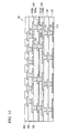
- FIGS. 13A to 13F are schematic sectional views showing wiring boards according to Examples 2 and 3 and Comparative Examples 1 to 4;
- FIGS. 15A to 15C are schematic sectional views showing a method of manufacturing the wiring board according to the second embodiment
- FIGS. 16A to 16C are schematic sectional views showing the method of manufacturing the wiring board according to the second embodiment.
- FIG. 17 is a schematic sectional view showing a wiring board according to a modification of the second embodiment.
- the wiring board 1 has the form of a “coreless board” not containing any support base material differently from a wiring board (a laminate obtained in such a manner that a required number of build-up layers are formed successively on both surfaces or one surface of a core board as a support base material) produced by a general build-up method.
- metal such as copper, copper alloy, etc. can be used as the material of each of the second to sixth wiring layers 21 , 31 , 42 , 51 and 61 .
- Parts of the first wiring layer 11 that is, a first principal surface 12 A (a lower surface in the drawing) of the first conductive layer 12 are exposed out of the first insulating layer 20 and serve as electrode pads 11 P electrically connected to a semiconductor chip 70 (see FIG. 2 ). That is, in this embodiment, a surface where the electrode pads 11 P are formed is provided as a chip mount surface.
- the planer shape of the first wiring layer 11 exposed out of the first insulating layer 20 is circular.
- the diameter of each circle can be set to be in a range of about 40 ⁇ m to about 120 ⁇ m.
- the pitch of the first wiring layer 11 exposed out of the first insulating layer 20 can be set to be in a range of about 100 ⁇ m to about 200 ⁇ m.
- the thickness of the first wiring layer 11 can be set to be in a range of about 10 ⁇ m to about 20 ⁇ m.
- the first insulating layer 20 is formed so that a second principal surface (an upper surface in the drawing) and side surfaces of the first wiring layer 11 are covered but the first principal surface 12 A of the first wiring layer 11 is exposed.
- An epoxy-based insulating resin having thermosetting characteristic can be used as the material of the first insulating layer 20 .
- the insulating resin is not limited to a resin having thermosetting characteristic but an insulating resin having photosensitivity may be used.
- the thickness of the first insulating layer 20 can be set to be in a range of about 15 ⁇ m to about 35 ⁇ m.
- the second wiring layer 21 is formed on the first insulating layer 20 .
- the second wiring layer 21 has via-wirings 21 a packed in via-holes VH 1 which are formed through the first insulating layer 20 to expose the upper surface of the first wiring layer 11 , and wiring patterns 21 b formed on the first insulating layer 20 .
- the via-wirings 21 a are electrically connected to the first wiring layer 11 (exposed in the bottoms of the via-holes VH 1 ).
- each of the via-holes VH 1 and the via-wirings 21 a formed in the via-holes VH 1 is tapered to have a shape having its diameter increasing as the position goes from the lower side (electrode pad 11 P (chip mount surface) side) to the upper side (sixth wiring layer 61 side) in FIG. 1 .
- the thickness of the wiring patterns 21 b of the second wiring layer 21 can be set to be in a range of about 20 ⁇ m to about 35 ⁇ m.
- the second insulating layer 30 is formed on the first insulating layer 20 so that the second wiring layer 21 is covered with the second insulating layer 30 .
- an insulating resin having the same composition as that of the first insulating layer 20 can be used as the material of the second insulating layer 30 .
- the thickness of the second insulating layer 30 can be set to be in a range of about 15 ⁇ m to about 35 ⁇ m.
- the third wiring layer 31 is formed on the second insulating layer 30 .
- the third wiring layer 31 has via-wirings 31 a packed in via-holes VH 2 which are formed through the second insulating layer 30 to expose the upper surface of the second wiring layer 21 , and wiring patterns 31 b formed on the second insulating layer 30 .
- the via-wirings 31 a are electrically connected to the second wiring layer 21 exposed in the bottoms of the via-holes VH 2 .
- each of the via-holes VH 2 and the via-wirings 31 a is tapered to have a shape having its diameter increasing as the position goes from the lower side to the upper side in FIG. 1 .
- the thickness of the wiring patterns 31 b of the third wiring layer 31 can be set to be in a range of about 20 ⁇ m to about 35 ⁇ m.
- the third insulating layer 40 has an insulating layer 40 A, and a contact layer 41 A.
- the insulating layer 40 A is formed on the second insulating layer 30 so that the upper surface and side surfaces of the third wiring layer 31 (specifically, the wiring patterns 31 b ) are covered with the insulating layer 40 A.
- the insulating layer 40 A is a reinforcing material-containing insulating layer, i.e. an insulating layer higher in mechanical strength (rigidity, hardness, etc.) than the other insulating layers 20 , 30 , 50 and 60 .
- an insulating resin obtained by adding a reinforcing material into a thermosetting resin can be used as the material of the insulating layer 40 A.
- a reinforcing material-containing insulating resin obtained by impregnating woven or unwoven fabric of glass, aramid or LCP (Liquid Crystal Polymer) fiber with an epoxy-based or polyimide-based thermosetting resin can be used as the material of the insulating layer 40 A.
- an insulating resin adjusted so that the glass transition temperature Tg of the insulating layer 40 A is higher (e.g. about 200° C. to 250° C.) than the glass transition temperature Tg (e.g. about 150° C.) of the other insulating layers 20 , 30 , 50 and 60 is used as the material of the insulating layer 40 A.
- the thickness of the insulating layer 40 A can be set to be in a range of about 30 ⁇ m to about 60 ⁇ m. It is preferable from the viewpoint of improving mechanical strength that the insulating layer 40 A is formed to be thicker than the other insulating layers 20 , 30 , 50 and 60 containing no reinforcing material.
- the contact layer 41 A is formed on the insulating layer 40 A so that the upper surface of the insulating layer 40 A is covered with the contact layer 41 A.
- the contact layer 41 A is an insulating layer which is higher in the degree of adhesion to a metal film (e.g. electroless plating) than the insulating layer 40 A and which is thinner than the insulating layer 40 A.
- the contact layer 41 A can be formed so as to be thinner than the wiring patterns 42 b of the fourth wiring layer 42 formed on the contact layer 41 A.
- the contact layer 41 A is formed on the insulating layer 40 A which covers the third wiring layer 31 as a lower layer, and the contact layer 41 A does not have to cover the wiring layer to keep insulation between formed wiring layers, unlike the insulating layer 40 A and the other insulating layers 20 , etc., the contact layer 41 A can be formed so as to be thinner than the wiring patterns 42 b . For this reason, it is preferable from the viewpoint of reduction in thickness of the wiring board 1 that the contact layer 41 A is set to be thinner than the wiring patterns 42 b . Speaking more, it is preferable from the viewpoint of reduction in warp of the wiring board 1 that the contact layer 41 A is set to be sufficiently thinner than the insulating layer 40 A.
- the thickness of the contact layer 41 A is not larger than 17% of the thickness of the insulating layer 40 A, and it is more preferable that the thickness of the contact layer 41 A is not larger than 10% of the thickness of the insulating layer 40 A.
- the thickness of the contact layer 41 A can be set to be in a range of about 0.5 ⁇ m to about 5 ⁇ m.
- an insulating resin containing a thermosetting resin containing an epoxy-based resin as its main component, and an inorganic filler can be used as the material of the contact layer 41 A.
- an insulating resin having a composition (e.g. epoxy resin and inorganic filler contents) adjusted so that the peel strength when the contact layer 41 A is electrolessly plated is at least higher than the peel strength (e.g. 100 to 200 N/m) when the insulating layer 40 A is electrolessly plated is preferred as the material of the contact layer 41 A.
- peel strength mentioned herein means a value (strength of peeling) indicating adhesion force between a conductor pattern (electroless plating) and an insulating layer.
- the peel strength is expressed in force (N/m) required for peeling a 1 m-wide conductor pattern from an insulating layer when the conductor pattern is pulled perpendicularly to be peeled from the insulating layer.
- the peel strength indicates that the adhesion strength between the conductor pattern and the insulating layer increases as the value of the force increases.
- An insulating resin adjusted so that the peel strength when the contact layer 41 A is electrolessly plated is not lower than 850 N/m which is higher than the peel strength (e.g. 600 N/m to 700 N/m) when the first insulating layer 20 is electrolessly plated is further preferred as the material of the contact layer 41 A. It is preferable that an insulating resin more excellent in chemical resistance (e.g.
- an insulating resin hardly etched by a desmear processing liquid is used as the material of the contact layer 41 A.
- an insulating resin adjusted so that the glass transition temperature Tg of the contact layer 41 A is not lower than 150° C. is used as the material of the contact layer 41 A.
- an insulating resin for example, containing 30 vol % or more of an epoxy resin, and a relatively small amount (e.g. 1 vol % to 50 vol %, both inclusively) of an inorganic filler is used as a specific material of the contact layer 41 A for achieving the aforementioned characteristic.
- an insulating resin containing 30 vol % to 65 vol % (both inclusively) of an epoxy resin, and 1 vol % to 30 vol % (both inclusively) of an inorganic filler is used as a specific material of the contact layer 41 A.
- the thermal expansion coefficient of the contact layer 41 A takes a relatively high value of about 40 ppm/° C. to about 100 ppm/° C. because the inorganic filler content is relatively small as described above.
- the contact layer 41 A is an insulating layer higher in surface smoothness than the insulating layer 40 A. That is, the upper surface of the contact layer 41 A (a surface opposite to a surface being in contact with the insulating layer 40 A) is an even smooth surface (low roughness surface). Specifically, the upper surface of the contact layer 41 A is a low roughness surface where shallow fine irregularities are formed. More specifically, the roughness of the upper surface of the contact layer 41 A is set to be in a range of 50 nm to 350 nm in terms of surface roughness Ra value.
- the surface roughness Ra value mentioned herein is a kind of numerical value expressing surface roughness and is called arithmetic average roughness. Specifically, the surface roughness Ra value is calculated in such a manner that the absolute value of a height varying in a measurement region is measured from a surface as an average line and subjected to arithmetic averaging.
- the fourth wiring layer 42 is formed on the contact layer 41 A.
- the fourth wiring layer 42 has via-wirings 42 a packed in via-holes VH 3 which are formed through the third insulating layer 40 (the insulating layer 40 A and the contact layer 41 A) to expose the upper surface of the third wiring layer 31 , and wiring patterns 42 b formed on the contact layer 41 A.
- the via-wirings 42 a are electrically connected to the third wiring layer 31 exposed in the bottoms of the via-holes VH 3 .
- each of the via-holes VH 3 and the via-wirings 42 a is tapered to have a shape having its diameter increasing as the position goes from the lower side to the upper side in FIG. 1 .
- the thickness of the wiring patterns 42 b of the fourth wiring layer 42 can be set to be in a range of about 20 ⁇ m to 35 ⁇ m.
- the fourth insulating layer 50 is formed on the contact layer 41 A so that the fourth wiring layer 42 is covered with the fourth insulating layer 50 .
- an insulating resin having the same composition as that of the first insulating layer 20 can be used as the material of the fourth insulating layer 50 .
- the thickness of the fourth insulating layer 50 can be set to be in a range of about 15 ⁇ m to about 35 ⁇ m.
- the fifth wiring layer 51 is formed on the fourth insulating layer 50 .
- the fifth wiring layer 51 has via-wirings 51 a packed in via-holes VH 4 which are formed through the fourth insulating layer 50 to expose the upper surface of the fourth wiring layer 42 , and wiring patterns 51 b formed on the fourth insulating layer 50 .
- the via-wirings 51 a are electrically connected to the fourth wiring layer 42 exposed in the bottoms of the via-holes VH 4 .
- each of the via-holes VH 4 and the via-wirings 51 a is tapered to have a shape having its diameter increasing as the position goes from the lower side to the upper side in FIG. 1 .
- the thickness of the wiring patterns 51 b of the fifth wiring layer 51 can be set to be in a range of about 20 ⁇ m to about 35 ⁇ m.
- the fifth insulating layer 60 is formed on the fourth insulating layer 50 so that the fifth wiring layer 51 is covered with the fifth insulating layer 60 .
- an insulating resin having the same composition as that of the first insulating layer 20 can be used as the material of the fifth insulating layer 60 .
- the thickness of the fifth insulating layer 60 can be set to be in a range of about 15 ⁇ m to about 35 ⁇ m.
- the sixth wiring layer 61 is an uppermost (outermost) wiring layer formed on the fifth insulating layer 60 .
- the sixth wiring layer 61 has via-wirings 61 a packed in via-holes VH 5 which are formed through the fifth insulating layer 60 to expose the upper surface of the fifth wiring layer 51 , and wiring patterns 61 b formed on the fifth insulating layer 60 .
- the via-wirings 61 a are electrically connected to the fifth wiring layer 51 exposed in the bottoms of the via-holes VH 5 .
- each of the via-holes VH 5 and the via-wirings 61 a is tapered to have a shape having its diameter increasing as the position goes from the lower side to the upper side in FIG. 1 .
- the thickness of the wiring patterns 61 b of the sixth wiring layer 61 can be set to be in a range of about 20 ⁇ m to about 35 ⁇ m.
- a solder resist layer 62 is formed on the outermost fifth insulating layer 60 on a side (upper side in FIG. 1 ) opposite to the surface where the electrode pads 11 P are formed.
- an epoxy-based insulating resin can be used as the material of the solder resist layer 62 .
- the thickness of the solder resist layer 62 can be set to be in a range of about 15 ⁇ m to about 35 ⁇ m.
- Opening portions 62 X for exposing parts of the wiring patterns 61 b of the sixth wiring layer 61 as external connection pads 61 P are formed in the solder resist layer 62 .
- the external connection pads 61 P are configured so that external connection terminals such as solder balls, lead pins, etc. which are used when the wiring board 1 is mounted in a mother board or the like can be connected to the external connection pads 61 P. That is, in this embodiment, the surface where the external connection pads 61 P are formed serves as an external connection terminal surface.
- a metal layer may be formed on each of the wiring patterns 61 b exposed out of the opening portions 62 X so that each of the external connection terminals can be connected to the metal layer.
- an Au layer, an Ni/Au layer (a metal layer formed in such a manner that an Ni layer and an Au layer are formed in this order), an Ni/Pd/Au layer (a metal layer formed in such a manner that an Ni layer, a Pd layer and an Au layer are formed in this order), etc. can be listed as examples of the metal layer.
- the wiring patterns 61 b exposed out of the opening portions 62 X (or a metal layer when the metal layer is formed on the wiring patterns 61 b ) may be directly used as external connection terminals.
- each of the opening portions 62 X (external connection pads 61 P) of the solder resist layer 62 is, for example, circular.
- the diameter of each circle can be set to be in a range of about 200 ⁇ m to about 1000 ⁇ m.
- the pitch of the external connection pads 61 P can be set to be in a range of about 500 ⁇ m to about 1200 ⁇ m.
- FIG. 2 The structure of a semiconductor package 2 using the wiring board 1 will be described below in accordance with FIG. 2 .
- the wiring board 1 in FIG. 2 is drawn to be upside down, compared with that in FIG. 1 .
- the semiconductor package 2 has a wiring board 1 , a semiconductor chip 70 connected to the wiring board 1 by flip chip bonding, and an underfill resin 72 .
- Solder 14 is formed on the electrode pads 11 P of the wiring board 1 .
- eutectic solder or lead (Pb)-free solder Sn—Ag-based, Sn—Cu-based, Sn—Ag—Cu-based, etc. can be used as the solder 14 .
- the semiconductor chip 70 has a circuit-forming surface (lower surface in FIG. 2 ) where bumps 71 are formed.
- the semiconductor chip 70 is electrically connected to the electrode pads 11 P of the wiring board 1 through the bumps 71 and the solder 14 .
- the underfill resin 72 is provided so that a gap between the wiring board 1 and the semiconductor chip 70 is filled with the underfill resin 72 .
- the underfill resin 72 is a resin for improving connection strength of connection portions between the bumps 71 and the electrode pads 11 P and for suppressing occurrence of corrosion or electromigration of the electrode pads 11 P to prevent reliability of the electrode pads 11 P from being lowered.
- an epoxy-based insulating resin can be used as the material of the underfill resin 72 .
- the insulating layer 40 A improved in mechanical strength by addition of a reinforcing material compared with the insulating layers 20 , 30 , 50 and 60 is provided so as to be located near the center in the direction of lamination of the wiring board 1 formed by lamination.
- the insulating layers 20 and 30 and the wiring layers 11 , 21 and 31 provided under the reinforcing material-containing insulating layer 40 A as the center are disposed so as to be substantially symmetrical with the insulating layers 50 and 60 and the wiring layers 42 , 51 and 61 provided above the reinforcing material-containing insulating layer 40 A as the center. Accordingly, vertical balance of the wiring board 1 with respect to the insulating layer 40 A as the center becomes so good that occurrence of warping in the wiring board 1 can be suppressed.
- the contact layer 41 A is formed on the reinforcing material-containing insulating layer 40 A, and the wiring patterns 42 b are formed on the contact layer 41 A.
- the contact layer 41 A is an insulating layer which has a low roughness surface as its upper surface (a surface where the wiring patterns 42 b are formed) and which is higher in adhesion to a metal film (electroless plating) than the insulating layer 40 A. For this reason, the wiring patterns 42 b formed on the low roughness surface of the contact layer 41 A can be provided as fine patterns.
- a method of manufacturing the wiring board 1 will be described below.
- a support board 80 is prepared as shown in FIG. 3A .
- a metal plate or metal foil can be used as the support board 80 .
- copper foil is used as the support board 80 .
- the thickness of the support board 80 is in a range of 35 ⁇ m to 100 ⁇ m.
- a resist layer 81 having opening portions 81 X is formed on one surface (upper surface in the drawing) of the support board 80 .
- the opening portions 81 X are formed so that portions of the upper surface of the support board 80 corresponding to regions where the first wiring layer 11 (see FIG. 1 ) will be formed are exposed.
- a photosensitive dry film or a liquid photo-resist e.g. a liquid resist made of a novolac-based resin, an epoxy-based resin, or the like
- a photo-resist e.g. a liquid resist made of a novolac-based resin, an epoxy-based resin, or the like
- the dry film is formed on the upper surface of the support board 80 by thermo-compression bonding and patterned by exposure and development to thereby form the resist layer 81 having opening portions 81 X of predetermined patterns corresponding to the regions where the first wiring layer 11 will be formed.
- the resist layer 81 can be also formed through the same step.
- electrolytic plating using the support board 80 as a plating power feeding layer is applied to the upper surface of the support board 80 while the resist layer 81 is used as a plating mask.
- electrolytic plating method by applying an electrolytic plating method to the upper surface of the support board 80 exposed out of the opening portions 81 X of the resist layer 81 , the first conductive layer 12 and the second conductive layer 13 are formed successively in the opening portions 81 X to form the first wiring layer 11 .
- the first conductive layer 12 has a structure in which an Au film, a Pd film and an Ni film are formed successively in this order, and the second conductive layer 13 is a Cu layer
- the first conductive layer 12 is first formed in such a manner that the Au film, the Pd film and the Ni film are formed successively by an electrolytic plating method using the support board 80 as a plating power feeding layer.
- the second conductive layer 13 is then formed in such a manner that the Cu layer is formed on the first conductive layer 12 by an electrolytic plating method using the support board 80 as a plating power feeding layer.
- the resist layer 81 shown in FIG. 3C is removed and the first insulating layer 20 is formed on the upper surface of the support board 80 so that the first wiring layer 11 is covered with the first insulating layer 20 .
- the first insulating layer 20 can be formed in such a manner that a resin film is formed on the support board 80 and then the resin film is heated at a temperature of about 130 to 150° C. while pressed so as to be hardened.
- the via-holes VH 1 are formed in predetermined places of the first insulating layer 20 so that the upper surface of the first wiring layer 11 is exposed.
- the via-holes VH 1 can be formed by a laser machining method using a carbon dioxide laser, a UV-YAG laser or the like.
- the required via-holes VH 1 may be formed by photolithography.
- the via-holes VH 1 of the first insulating layer 20 are filled with a via-conductor so that via-wirings 21 a are formed and wiring patterns 21 b electrically connected to the first wiring layer 11 through the via-wirings 21 a are formed on the first insulating layer 20 .
- These via-wirings 21 a and wiring patterns 21 b can be formed by one of various wiring forming methods such as a semi-additive method, a subtractive method, etc.
- the steps shown in FIGS. 3D to 4A are repeated to laminate the second insulating layer 30 and the third wiring layer 31 . That is, as shown in FIG. 4B , the second insulating layer 30 is formed on the first insulating layer 20 and the second wiring layer 21 , and the via-holes VH 2 reaching the upper surfaces of the wiring patterns 21 b are formed in the second insulating layer 30 . Then, via-wirings 31 a are formed in the via-holes VH 2 , and wiring patterns 31 b electrically connected to the via-wirings 31 a are formed.
- an insulating layer 40 B serving as an insulating layer 40 A (see FIG. 1 ) is prepared, that is, a reinforcing material-containing insulating layer 40 B made of woven or unwoven fabric of glass, aramid or LCP (Liquid Crystal Polymer) fiber impregnated with an unhardened thermosetting resin is prepared.
- a B-stage (semi-hardened state) layer is used as the insulating layer 40 B.
- the thickness of the insulating layer 40 B can be set to be in a range of 30 ⁇ m to 80 ⁇ m.
- a structure 82 A in which an insulating layer 41 B serving as a contact layer 41 A (see FIG. 1 ) is bonded to a carrier 82 is prepared.
- An insulating resin containing 30 vol % or more of an unhardened epoxy resin, and 1 to 50 vol % of an inorganic filler can be used as the material of the insulating layer 41 B.
- a semi-hardened state layer is used as the insulating layer 41 B.
- the thickness of the insulating layer 41 B can be set to be in a range of about 1 ⁇ m to about 4 ⁇ m.
- copper foil can be used as the carrier 82 for carrying the insulating layer 41 B.
- the thickness of the carrier 82 can be set to be in a range of about 2 ⁇ m to about 18 ⁇ m.
- the insulating layer 40 B and the structure 82 A are disposed sequentially from bottom on the upper surface side of the structure shown in FIG. 4B .
- the structure 82 A is disposed in a state where the insulating layer 41 B faces downward so that the insulating layer 41 B faces the insulating layer 40 B.
- the structure shown in FIG. 4B the insulating layer 40 B and the structure 82 A are pressed while heated at a temperature of about 190° C. to about 250° C. in a vacuum atmosphere from both sides. Consequently, as shown in FIG.
- the insulating layers 40 B and 41 B are hardened so that the insulating layer 40 A and the contact layer 41 A are formed on the second insulating layer 30 and the third wiring layer 31 .
- the second insulating layer 30 and the third wiring layer 31 are bonded to the insulating layer 40 A while the insulating layer 40 A is bonded to the contact layer 41 A. Consequently, the third insulating layer 40 in which the insulating layer 40 A and the contact layer 41 A are formed in this order is formed on the second insulating layer 30 and the third wiring layer 31 .
- the thickness of the insulating layer 40 A after lamination is about 40 ⁇ m.
- the carrier 82 (copper foil) shown in FIG. 5A is selectively removed from the contact layer 41 A.
- wet etching using an aqueous solution of ferric chloride, an aqueous solution of cupric chloride, an aqueous solution of ammonium persulfate or the like can be used for selectively removing the carrier 82 (copper foil) from the contact layer 41 A.
- the via-holes VH 3 are formed in predetermined places of the insulating layer 40 A and the contact layer 41 A so that the upper surfaces of the wiring patterns 31 b of the third wiring layer 31 are exposed.
- the via-holes VH 3 can be formed by a laser machining method using a carbon dioxide laser, a UV-YAG laser or the like.
- the via-holes VH 3 formed by a laser machining method are provided as concave portions each shaped like a frustum of a circular cone which has an opening portion on a side where the fourth insulating layer 50 (see FIG. 1 ) will be formed, and a bottom formed by the upper surface of the third wiring layer 31 so that the area of the opening portion is larger than the area of the bottom.
- desmear processing is then performed to remove a resin residue of the insulating layer 40 A and the contact layer 41 A deposited on the upper surface of the third wiring layer 31 exposed in the bottoms of the via-holes VH 3 .
- this desmear processing can be performed by a permanganate method or the like.
- a desmear liquid (etchant) is also fed to the surface of the contact layer 41 A, so that the surface of the contact layer 41 A is etched with the desmear liquid, and the surface of the contact layer 41 A is roughened.
- the contact layer 41 A is less subject to the desmear processing, that is, the contact layer 41 A is excellent in desmear resistance because the thermosetting resin (epoxy-based resin in the contact layer 41 A) content is high to be not lower than 30 vol % and the inorganic filler content is relatively low to be in the range of 1-50 vol %, compared with the insulating layer 40 A.
- the contact layer 41 A is hardly etched with the desmear liquid so that the surface of the contact layer 41 A is kept as low roughness after the desmear processing.
- the roughness of the surface of the contact layer 41 A after the desmear processing is kept at a low value of about 50-350 nm in terms of surface roughness Ra value.
- the composition (e.g. epoxy-based resin content and inorganic filler content) of the contact layer 41 A is adjusted to obtain such desmear resistance that the roughness of the surface of the contact layer 41 A after the desmear processing can be kept at a low value of about 50-350 nm in terms of surface roughness Ra value even when the desmear processing is performed.
- a seed layer 83 of copper or the like is formed on the upper surfaces of the wiring patterns 31 b exposed in the bottoms of the via-holes VH 3 , the inner wall surfaces of the via holes VH 3 and the upper surface of the contact layer 41 A.
- the seed layer 83 is formed by an electroless copper plating method or a sputtering method.
- the inorganic filler content of the contact layer 41 A causing lowering of adhesion to the seed layer 83 is so relatively low that the seed layer 83 adheres to the contact layer 41 A well.
- the inorganic filler content of the contact layer 41 A is equal to or lower than the inorganic filler content of an interlayer insulating layer (the first insulating layer 20 or the like) containing no reinforcing material. For this reason, the adhesion strength between the contact layer 41 A and the seed layer 83 is equal to or higher than the adhesion strength between the first insulating layer 20 and the seed layer. Moreover, because the roughness of the upper surface of the contact layer 41 A is low as described above, the fourth wiring layer 42 formed on the contact layer 41 A can be provided as a fine line structure.
- a dry film resist (DFR) or the like having opening portions 84 X corresponding to the patterns of the fourth wiring layer 42 is used for forming a resist layer 84 on the seed layer 83 .
- this resist layer 84 is formed by photolithography.
- the opening portions 84 X of the resist layer 84 containing the via-holes VH 3 are filled with a metal plating layer 42 C of copper or the like by an electrolytic plating method using the seed layer 83 as a power feeding layer.
- plating is performed on the inside from the seed layer 83 , so that the via-holes VH 3 are filled with a via-conductor 42 D. Consequently, via-wirings 42 a constituted by the seed layer 83 and the via-conductor 42 D are formed, and wiring patterns 42 b constituted by the seed layer 83 and the metal plating layer 42 C are formed.
- the wiring patterns 42 b are formed on the contact layer 41 A of the low roughness surface as described above, so that the wiring patterns 42 b can be provided as a fine line structure.
- the resist layer 84 shown in FIG. 6C is removed and then the unnecessary seed layer 83 is removed by etching while the metal plating layer 42 C and the via-conductor 42 D are used as a mask.
- the fourth wiring layer 42 having the via-wirings 42 a and the wiring patterns 42 b is formed on the insulating layer 40 A and the contact layer 41 A. That is, the fourth wiring layer 42 is formed by a semi-additive method.
- the steps shown in FIGS. 3D to 4A are repeated again to laminate insulating layers and wiring layers alternately. That is, as shown in FIG. 7B , a fourth insulating layer 50 is formed on the contact layer 41 A and the fourth wiring layer 42 , and via-holes VH 4 reaching the upper surface of the fourth wiring layer 42 are formed in the fourth insulating layer 50 . Then, via-wirings 51 a are formed in the via-holes VH 4 , and wiring patterns 51 b electrically connected to the via-wirings 51 a are formed to thereby provide a fifth wiring layer 51 .
- a fifth insulating layer 60 is formed on the fourth insulating layer 50 and the fifth wiring layer 51 , and via-holes VH 5 reaching the upper surfaces of the wiring patterns 51 b are formed in the fifth insulating layer 60 .
- via-wirings 61 a are formed in the via-holes VH 5 , and wiring patterns 61 b electrically connected to the via-wirings 61 a are formed to thereby provide a sixth wiring layer 61 .
- a solder resist layer 62 having opening portions 62 X for exposing external connection pads 61 P set in required places of the sixth wiring layer 61 is formed on the fifth insulating layer 60 and the sixth wiring layer 61 .
- this solder resist layer 62 can be formed in such a manner that a photosensitive solder resist film is formed or a liquid solder resist is applied so that the resist is patterned into a required shape. Consequently, parts of the sixth wiring layer 61 are exposed as external connection pads 61 P out of the opening portions 62 X of the solder resist layer 62 .
- a metal layer for example, obtained by laminating an Ni layer and an Au layer in this order may be formed on the external connection pads 61 P.
- this metal layer can be formed by an electroless plating method.
- the support board 80 (see FIG. 7B ) used as a temporary board is removed.
- the support board 80 can be removed by wet etching using an aqueous solution of ferric chloride, an aqueous solution of cupric chloride, an aqueous solution of ammonium persulfate or the like.
- the outermost layer of the first wiring layer 11 exposed out of the first insulating layer 20 is an Au film or the like, so that only the support board 80 provided as copper foil can be etched selectively.
- the sixth wiring layer 61 is a copper layer, it is necessary to perform the aforementioned wet etching while using the sixth wiring layer 61 as a mask in order to prevent the sixth wiring layer 61 exposed in the bottoms of the opening portions 62 X from being etched together with the support board 80 .
- the wiring board 1 according to this embodiment can be produced.
- solder 14 is formed on the electrode pads 11 P of the wiring board 1 .
- the solder 14 can be formed by applying solder paste or mounting solder balls.
- a semiconductor chip 70 having terminals on which bumps 71 are formed is positioned on the electrode pads 11 P, and the solder 14 and the bumps 71 are melted so that the semiconductor chip 70 is electrically connected to the electrode pads 11 P (flip chip bonding).
- a gap between the semiconductor chip 70 and the first insulating layer 20 of the wiring board 1 is filled with a liquid underfill resin 72 , and the liquid underfill resin 72 is hardened.
- the contact layer 41 A is formed on the reinforcing material-containing insulating layer 40 A and the wiring patterns 42 b are formed on the contact layer 41 A.
- the contact layer 41 A is an insulating layer which has an upper surface (a surface where the wiring patterns 42 b are formed) provided as a low roughness surface and which is higher in adhesion to a metal film (electroless plating) than the insulating layer 40 A.
- the wiring patterns 42 b formed on the low roughness surface of the contact layer 41 A can be provided as fine patterns.
- the wiring patterns 42 b are formed on the contact layer 41 A which is more excellent in desmear resistance than the reinforcing material-containing insulating layer 40 A.
- the surface roughness of the upper surface of the contact layer 41 A after desmear processing is kept at a low value of 50 to 350 nm in terms of surface roughness Ra value. For this reason, when the wiring patterns 42 b are formed on such an upper surface (low roughness surface) of the contact layer 41 A, a semi-additive method can be used for forming fine wiring.
- the wiring layers 11 , 21 and 31 and the insulating layers 20 and 30 are supported by the support board 80 when the wiring layers 11 , 21 and 31 and the insulating layers 20 and 30 are formed. Accordingly, occurrence of warping can be suppressed favorably. Moreover, because the wiring layers 11 , 21 and 31 and the insulating layers 20 and 30 are formed while supported by the support board 80 having high rigidity, the problem of thin board conveyance which may occur at the time of production of the wiring board can be prevented from occurring.
- the third insulating layer 40 containing the insulating layer 40 A high in mechanical strength is formed by lamination.
- the wiring layers 42 , 51 and 61 and the insulating layers 50 and 60 are formed on the third insulating layer 40 containing the insulating layer 40 A high in mechanical strength. For this reason, the wiring layers 42 , 51 and 61 and the insulating layers 50 and 60 are supported by the third insulating layer 40 and the support board 80 , so that occurrence of warping can be suppressed favorably even when the wiring layers 42 , 51 and 61 and the insulating layers 50 and 60 are formed.
- the wiring board 1 can be produced without largely altering the multilayer wiring board producing process heretofore performed, reduction in equipment cost can be attained. Thus, reduction in production cost of the wiring board 1 can be attained.
- the insulating layer 40 A more improved in mechanical strength than the insulating layers 20 , 30 , 50 and 60 by addition of a reinforcing material is provided so as to be located near the center in the direction of lamination of the wiring board 1 formed by lamination. Consequently, the insulating layers 20 and 30 and the wiring layers 11 , 21 and 31 provided in the lower portion with respect to the reinforcing material-containing insulating layer 40 A provided as the center are disposed so as to be substantially symmetrical with the insulating layers 50 and 60 and the wiring layers 42 , 51 and 61 provided in the upper portion with respect to the reinforcing material-containing insulating layer 40 A provided as the center.
- the first embodiment can be carried out in the following forms which have been changed properly.
- the insulating layer 40 having the reinforcing material-containing insulating layer 40 A and the contact layer 41 A having low roughness and improved in adhesion to electroless plating is provided near the center in the direction of lamination.
- the invention is not limited thereto as long as at least one of interlayer insulating layers formed in the wiring board is the insulating layer 40 having the insulating layer 40 A and the contact layer 41 A. Accordingly, the position where the insulating layer 40 is formed and the number of such insulating layers 40 are not particularly limited.
- a plurality of insulating layers 40 each having a reinforcing material-containing insulating layer 40 A and a contact layer 41 A may be provided near the center in the direction of lamination. That is, a wiring board 1 A having the two insulating layers 40 is configured so that an insulating layer 40 (upper insulating layer 40 ) and a wiring layer 43 formed on the insulating layer 40 are added to the wiring board 1 shown in FIG. 1 .
- the wiring layer 43 has via-wirings 43 a packed in via-holes VH 6 which are formed through the reinforcing material-containing insulating layer 40 A and the contact layer 41 A to expose the upper surface of the wiring layer 42 , and wiring patterns 43 b formed on the contact layer 41 A.
- the rigidity of the wiring board 1 A can be more improved in the vicinity of the center in the direction of lamination. Consequently, the reinforcing effect based on the insulating layers 40 can be improved so that warping of the wiring board 1 A can be reduced effectively.
- the plurality of insulating layers 40 exhibit the same effect as in a core board (support member) having high rigidity.
- the wiring layers 42 and 43 formed on the plurality of insulating layers 40 are interlayer-connected through via-wirings 42 a and 43 a packed in the via-holes VH 3 and VH 6 formed in the insulating layers 40 respectively. It is easy to form such via-wirings 42 a and 43 a finely and voidlessly. For this reason, increase in total density of the wiring board can be achieved so that reliability of interlayer connection of the wiring layers can be improved.
- the interlayer insulating layer which is the outermost layer on the external connection terminal surface side may be replaced by an insulating layer 40 having a reinforcing material-containing insulating layer 40 A and a contact layer 41 A. That is, in a wiring board 1 B, the fifth insulating layer 60 in the wiring board 1 in FIG. 1 is replaced by an insulating layer 40 , and the insulating layer 40 in the wiring board 1 is replaced by an insulating layer 44 containing no reinforcing material.
- a wiring layer 63 formed on the insulating layer 40 has via-wirings 63 a packed in via-holes VH 7 which are formed through the reinforcing material-containing insulating layer 40 A and the contact layer 41 A to expose the upper surface of the wiring layer 51 , and wiring patterns 63 b formed on the contact layer 41 A.
- the wiring layer 63 exposed out of the opening portions 62 X of the solder resist layer 62 serves as external connection pads 63 P.
- the insulating layer 40 having the reinforcing material-containing insulating layer 40 A and the contact layer 41 A may be provided so as to be biased toward the external connection terminal surface side.
- the insulating layer 40 having the reinforcing material-containing insulating layer 40 A and the contact layer 41 A may be provided so as to be biased toward the chip mounting surface side.
- all interlayer insulating layers may be replaced by insulating layers 40 each having a reinforcing material-containing insulating layer 40 A and a contact layer 41 A. That is, in a wiring board 1 C, all the insulating layers 20 , 30 , 50 and 60 in the wiring board 1 shown in FIG. 1 are replaced by the insulating layers 40 . In this case, warping of the wiring board 1 C can be reduced effectively. For example, when there is the possibility that warping of the wiring board 1 C will become intensive in consideration of stress of materials, etc.
- the interlayer insulating layers are replaced by the insulating layers 40 each having the reinforcing material-containing insulating layer 40 A and the contact layer 41 A as described in this modification.
- any one of the interlayer insulating layers to be formed may be replaced by the insulating layer 40 having the insulating layer 40 A and the contact layer 41 A.
- any insulating layer can be replaced by the insulating layer 40 . That is, any insulating layer can be replaced by the insulating layer 40 suitably in accordance with characteristic (the number of built-up layers, the thickness of each layer, the area occupied by each wiring layer, etc.) of the wiring board.
- the inorganic filler content of the contact layer 41 A is so relatively small that the thermal expansion coefficient of the contact layer 41 A becomes higher (e.g. about 40-100 ppm/° C.) than those of the other insulating layers 20 , 30 , 40 A, etc.
- the thermal expansion coefficient of the contact layer 41 A is largely different from the thermal expansion coefficient (e.g. about 17 ppm/° C.) of a wiring layer (copper). For this reason, there is the possibility that warping may occur in the wiring board 1 because of the difference between the thermal expansion coefficients.
- warping of the wiring board is improved by addition of the reinforcing material-containing insulating layer 40 A and the fine structure of wiring patterns is achieved by formation of the contact layer 41 A but there is the possibility that addition of the contact layer 41 A will exert a bad influence on improvement in warping due to the insulating layer 40 A. Therefore, as shown in FIGS.
- simulation of warping is applied on each of wiring boards (Examples 1 to 3) in which at least one insulating layer 40 having an insulating layer 40 A and a contact layer 41 A is provided, wiring boards (Comparative Examples 1 to 3) in which only an insulating layer 40 A is provided in place of each insulating layer 40 and a wiring board (Comparative Example 4) in which the insulating layer 40 A and the contact layer 41 A are not provided.
- the wiring board according to Example 1 is formed in such a manner that seven wiring layers C 1 to C 7 and six insulating layers A 1 to A 6 are formed alternately and a solder resist layer SR is formed on the lowermost insulating layer A 6 .
- the wiring board is formed by successively laminating the chip mounting surface side wiring layers C 1 to C 7 and insulating layers A 1 to A 6 on the support board in the same manner as in the method of manufacturing the wiring board 1 according to the first embodiment.
- the insulating layer A 4 is an insulating layer 40 which is a laminate of a reinforcing material-containing insulating layer 40 A and a contact layer 41 A, and the other insulating layers A 1 to A 3 , A 5 and A 6 are insulating layers containing no reinforcing material.
- the thermal expansion coefficient and Young's modulus of the insulating layer 40 A are adjusted to 16.5 ppm/° C. and about 30000 MPa respectively and the thermal expansion coefficient and Young's modulus of the contact layer 41 A are adjusted to 70-90 ppm/° C. and about 2000 MPa respectively to thereby adjust the thermal expansion coefficient and Young's modulus of the insulating layer 40 to 17.0 ppm/° C. and about 29000 MPa respectively.
- the thermal expansion coefficient and Young's modulus of the insulating layer containing no reinforcing material are adjusted to 39 ppm/° C. and about 5000 MPa respectively, and the thermal expansion coefficient and Young's modulus of the solder resist layer SR are adjusted to 40 ppm/° C. and about 3800 MPa respectively.
- the planer shape of the wiring board is provided as a rectangular shape of 45 mm ⁇ 45 mm.
- the layer thicknesses of the wiring layers C 1 to C 7 are set to be 15 ⁇ m
- the layer thickness of the insulating layer A 1 is set to be 15 ⁇ m
- the layer thicknesses of the insulating layers A 2 , A 3 , A 5 and A 6 containing no reinforcing material are set to be 30 ⁇ m
- the layer thickness of the reinforcing material-containing wiring layer A 4 is set to be 40 ⁇ m
- the layer thickness of the solder resist layer SR is set to be 15 ⁇ m.
- the layer thickness (40 ⁇ m) of the insulating layer A 4 which is the insulating layer 40 is the sum of the thickness (38 ⁇ m) of the insulating layer 40 A and the thickness (2 ⁇ m) of the contact layer 41 A.
- the Cu areas of the wiring layers C 1 to C 7 are adjusted so that the remaining copper ratios of the wiring layers C 1 to C 7 are 1.5%, 66.8%, 88.6%, 62.3%, 82.5%, 76.1% and 82.2% respectively.
- the remaining copper ratio is a ratio of the area of a copper layer for forming a wiring layer to the area on an insulating layer.
- the wiring board according to Example 2 is formed so that the insulating layers A 3 and A 5 are provided as the insulating layers 40 in addition to the insulating layer A 4 provided as the insulating layer 40 .
- the wiring board according to Example 3 is formed so that all the insulating layers A 1 to A 6 are provided as the insulating layers 40 .
- the wiring board according to Comparative Example 1 is formed so that the contact layer 41 A is removed from the insulating layer A 4 of the wiring board according to Example 1 and the insulating layer 40 of the wiring board according to Example 1 is replaced by the reinforcing material-containing insulating layer 40 A singly.
- the wiring board according to Comparative Example 2 is formed so that the contact layers 41 A are removed from the insulating layers A 3 to A 5 of the wiring board according to Example 2 and the insulating layers 40 of the wiring board according to Example 2 are replaced by the reinforcing material-containing insulating layers 40 A singly and respectively.
- the wiring board according to Comparative Example 3 is formed so that the contact layers 41 A are removed from the insulating layers A 1 to A 6 of the wiring board according to Example 3 and the insulating layers 40 of the wiring board according to Example 3 are replaced by the reinforcing material-containing insulating layers 40 A singly and respectively.
- the wiring board according to Comparative Example 4 is formed so that all the insulating layers A 1 to A 6 are provided as insulating layers containing no reinforcing material.
- the thickness of the insulating layer A 1 is set to be 15 ⁇ m
- the thicknesses of the other insulating layers A 2 to A 6 are set to be 30 ⁇ m.
- Warping is measured when the temperature is reduced to 25 degrees after stress is released in the condition that the wiring board according to each example is put under an environment of 190 degrees. As shown in FIG. 12C , warping is measured as a difference in height between respective end portions in a half diagonal length of the wiring board, that is, between a board center portion B 1 and a corner portion B 2 . Incidentally, simulation results are shown in Table 1 while the amount of warping in the case where the chip mounting surface is convexly warped is regarded as plus and the amount of warping in the case where the chip mounting surface is concavely warped is regarded as minus.
- the amount of warping is ⁇ 671 ⁇ m.
- the amounts of warping are ⁇ 643 ⁇ m, ⁇ 561 ⁇ m and ⁇ 89 ⁇ m, respectively. It is found that the amount of warping in each of Examples 1 to 3 is smaller than the amount of warping in Comparative Example 4.
- the thickness of the contact layer 41 A is adjusted to about 5.3% of the thickness of the insulating layer 40 A, and the Young's modulus of the contact layer 41 A is adjusted to about 6.7% of the Young's modulus of the insulating layer 40 A.
- the contact layer 41 A is sufficiently thinner than the insulating layer 40 A and the Young's modulus of the contact layer 41 A is smaller than that of the insulating layer 40 A. Accordingly, it is thought of that a function of weakening the warping improvement effect due to the reinforcing material-containing insulating layer 40 A is so small that the contact layer 41 A does not exert a bad influence on the warping improvement.
- Example 3 in which all the insulating layers A 1 to A 6 are provided as the insulating layers 40 (each composed of a reinforcing material-containing insulating layer 40 A and a contact layer 41 A), it is found that a high warping improvement effect is obtained because the amount of warping is ⁇ 89 ⁇ m.
- the absolute value of the amount of warping in Example 3 is 50 ⁇ m or more larger than that in Comparative Example 3. It is thought of that this is because the influence of the thermal expansion coefficient (or Young's modulus) of the contact layer 41 on the amount of warping increases as the absolute value of the amount of warping decreases.
- the difference in the amount of warping increases in accordance with the presence/absence of the contact layer 41 A.
- the difference in the amount of warping is a difference generated when the absolute value of the amount of warping becomes sufficiently small. Accordingly, as is obvious from the simulation results, it can be said that the warping improvement effect due to the insulating layer 40 having the contact layer 41 A is obtained sufficiently even when the difference in the amount of warping between Example 3 and Comparative Example 3 increases.
- FIGS. 14 , 15 A- 15 C and 16 A- 16 C A second embodiment will be described below with reference to FIGS. 14 , 15 A- 15 C and 16 A- 16 C.
- the first embodiment has been described about a wiring board formed by alternately laminating wiring layers and insulating layers from the chip mounting surface side. On the contrary, this embodiment will be described about a wiring board formed by alternately laminating wiring layers and insulating layers from the external connection terminal surface side.
- the first embodiment is configured so that an insulating layer having a reinforcing material-containing insulating layer and a contact layer is provided near the center in the direction of lamination
- this embodiment is configured so that an insulating layer having a reinforcing material-containing insulating layer and a contact layer is provided as the outermost layer on the external connection terminal surface side.
- a wiring board 3 has a structure in which a first wiring layer 111 , a first insulating layer 120 , a second wiring layer 122 , a second insulating layer 130 , a third wiring layer 131 , a third insulating layer 140 , a fourth wiring layer 141 , a fourth insulating layer 150 , a fifth wiring layer 151 , a fifth insulating layer 160 and a sixth wiring layer 161 are formed successively.
- the wiring board 3 according to this embodiment has the form of a “coreless board” containing no support based material, similarly to the wiring board 1 according to the first embodiment.
- metal such as copper or copper alloy can be used as each of the materials of the first to sixth wiring layers 122 , 131 , 141 , 151 and 161 .
- the first wiring layer 111 is formed as the lowermost layer in FIG. 14 .
- the first wiring layer 111 has a first conductive layer 112 , and a second conductive layer 113 .
- a conductive layer in which an Au film, a Pd film and an Ni film are formed successively in this order so that the Au film is exposed out of the wiring board 3 can be used as the first conductive layer 112 .
- a conductive layer containing a Cu layer or the like can be used as the second conductive layer 113 .
- Parts of the first wiring layer 111 that is, a first principal surface 112 A (a lower surface in the drawing) of the first conductive layer 112 are exposed out of the first insulating layer 20 and serve as external connection pads 111 P to which external connection terminals such as solder balls, lead pins, etc. used when the wiring board 3 is mounted in a mother board or the like are connected. That is, in this embodiment, a surface where the external connection pads 111 P are formed is provided as an external connection terminal surface.
- the first principal surface 112 A of the first conductive layer 112 is on the same plane with the first principal surface (lower surface in the drawing) of the first insulating layer 120 .
- the first wiring layer 111 per se exposed out of the first insulating layer 120 may be used as external connection terminals.
- the planer shape of the first wiring layer 111 exposed out of the first insulating layer 120 is circular.
- the diameter of each circle can be set to be in a range of about 200 ⁇ m to about 1000 ⁇ m.
- the pitch of the first wiring layer 111 exposed out of the first insulating layer 120 can be set to be in a range of about 500 ⁇ m to about 1200 ⁇ m.
- the thickness of the first wiring layer 111 can be set to be in a range of about 10 ⁇ m to about 20 ⁇ m.
- the first insulating layer 120 has an insulating layer 120 A, and a contact layer 121 A.
- the insulating layer 120 A is formed so that the second principal surface (upper surface in the drawing) and side surfaces of the first wiring layer 111 are covered with the insulating layer 120 A but the first principal surface 112 A of the first wiring layer 111 is exposed.
- the insulating layer 120 A is an insulating layer which has the same composition as the insulating layer 40 A in the first embodiment, i.e. a reinforcing material-containing insulating layer.
- An epoxy-based insulating resin having thermosetting characteristic can be used as the material of the insulating layer 120 A.
- the insulating resin is not limited to the resin having thermosetting characteristic but an insulating resin having photosensitivity can be used.
- the thickness of the insulating layer 120 A can be set to be in a range of about 30 ⁇ m to about 60 ⁇ m.
- the contact layer 121 A is formed on the insulating layer 120 A so that the upper surface of the insulating layer 120 A is covered with the contact layer 121 A.
- the contact layer 121 A is an insulating layer which has the same composition as the contact layer 41 A in the first embodiment, i.e. an insulating layer which has a surface smoother (lower roughness) than the insulating layer 120 A and which is higher in adhesion to a metal film (e.g. electroless plating) than the insulating layer 120 A.
- an insulating resin containing 30 vol % or more of an epoxy resin, and 1 to 50 vol % of an inorganic filler can be used as the material of the contact layer 121 A.
- the surface roughness of the contact layer 121 A is set to be in a range of 50 to 350 nm in terms of surface roughness Ra value.
- the thickness of the contact layer 121 can be set to be in a range of about 0.5 ⁇ m to about 5 ⁇ m.
- the second wiring layer 122 is formed on the first insulating layer 120 .
- the second wiring layer 122 has via-wirings 122 a packed in via-holes VH 11 which are formed through the insulating layer 120 A and the contact layer 121 A to expose the upper surface of the first wiring layer 111 , and wiring patterns 122 b formed on the contact layer 121 A.
- the via-wirings 122 a are electrically connected to the first wiring layer 111 exposed in the bottoms of the via-holes VH 11 .
- each of the via-holes VH 11 and the via-wirings 122 a is tapered to have a shape having its diameter increasing as the position goes from the lower side (external connection terminal surface side) to the upper side (sixth wiring layer 161 side) in FIG. 14 .
- the thickness of the wiring patterns 122 b of the second wiring layer 122 can be set to be in a range of about 20 ⁇ m to about 35 ⁇ m.
- the third to sixth wiring layers 131 , 141 , 151 and 161 are formed with interposition of the second to fifth insulating layers 130 , 140 , 150 and 160 and interlayer-connected through via-wirings 131 a , 141 a , 151 a and 161 a packed in via-holes VH 12 , VH 13 , VH 14 and VH 15 formed in the insulating layers 130 , 140 , 150 and 160 respectively.
- an epoxy-based insulating resin having thermosetting characteristic can be used as each of the materials of the second to fifth insulating layers 130 , 140 , 150 and 160 .
- the insulating resin is not limited to the resin having thermosetting characteristic but an insulating resin having photosensitivity can be used.
- the thicknesses of the second to fifth insulating layers 130 , 140 , 150 and 160 can be set to be in a range of about 15 ⁇ m to about 35 ⁇ m.
- the third wiring layer 131 has via-wirings 131 a electrically connected to the wiring patterns 122 b of the second wiring layer 122 , and wiring patterns 131 b electrically connected to the via-wirings 131 a .
- the fourth wiring layer 141 has via-wirings 141 a electrically connected to the wiring patterns 131 b , and wiring patterns 141 b electrically connected to the via-wirings 141 a .
- the fifth wiring layer 151 has via-wirings 151 a electrically connected to the wiring patterns 141 b , and wiring patterns 151 b electrically connected to the via-wirings 151 a .
- the sixth wiring layer 161 has via-wirings 161 a electrically connected to the wiring patterns 151 b , and wiring patterns 161 b electrically connected to the via-wirings 161 a .
- Each of the via wirings 131 a , 141 a , 151 a and 161 a of the third to sixth wiring layers 131 , 141 , 151 and 161 is tapered to have a shape having its diameter increasing as the position goes from the lower side (external connection pad 111 P side) to the upper side (wiring pattern 161 b side) in FIG. 14 .
- each of the via-wirings 131 a , 141 a , 151 a and 161 a is shaped like a frustum of a circular cone so that the diameter of an end surface on the external connection pad 111 P side is smaller than the diameter of an end surface on the wiring pattern 161 b side.
- a solder resist layer 162 is formed on the fifth insulating layer 160 .
- an epoxy-based insulating resin can be used as the material of the solder resist layer 162 .
- the thickness of the solder resist layer 162 can be set to be in a range of about 15 ⁇ m to about 35 ⁇ m.
- Opening portions 162 X for exposing parts of the wiring patterns 161 b as electrode pads 161 P are formed in the solder resist layer 162 .
- the electrode pads 161 P are configured so that, for example, a semiconductor chip or the like can be electrically connected to the electrode pads 161 P. That is, in this embodiment, a surface where the electrode pads 161 P are formed is provided as a chip mounting surface.
- a metal layer may be formed on each of the wiring patterns 161 b of the sixth wiring layer 161 exposed out of the opening portions 162 X so that a semiconductor chip can be connected to the metal layer.
- An Au layer, an Ni/Au layer (a metal layer formed in such a manner that an Ni layer and an Au layer are formed in this order), an Ni/Pd/Au layer (a metal layer formed in such a manner that an Ni layer, a Pd layer and an Au layer are formed in this order), etc. can be listed as examples of the metal layer.
- each of the opening portions 162 X (electrode pads 161 P) of the solder resist layer 162 is, for example, circular.
- the diameter of each circle can be set to be in a range of about 40 ⁇ m to about 120 ⁇ m.
- the pitch of the electrode pads 161 P can be set to be in a range of about 100 ⁇ m to about 200 ⁇ m.
- a support board 180 is prepared as shown in FIG. 15A .
- a metal plate or metal foil can be used as the support board 180 .
- copper foil is used as the support board 180 .
- the thickness of the support board 180 is in a range of 35 ⁇ m to 100 ⁇ m.
- a resist layer 181 having opening portions 181 X corresponding to the shape of the first wiring layer 111 is formed on one surface (upper surface in the drawing) of the support board 180 .
- electrolytic plating using the support board 180 as a plating power feeding layer is applied to the upper surface of the support board 180 .
- an electrolytic plating method is applied to the upper surface of the support board 180 exposed out of the opening portions 181 X of the resist layer 181 to thereby laminate the first conductive layer 112 and the second conductive layer 113 successively in the opening portions 181 X to form the first wiring layer 111 .
- the first conductive layer 112 has a structure in which an Au film, a Pd film and an Ni film are formed successively in this order
- the second conductive layer 113 is a Cu layer
- an Au film, a Pd film and an Ni film are first formed in this order by an electrolytic plating method using the support board 180 as a plating power feeding layer to thereby form the first conductive layer 112 .
- a Cu layer is then formed on the first conductive layer 112 by an electrolytic plating method using the support board 180 as a plating power feeding layer to thereby form the second conductive layer 113 .
- an insulating layer 120 B serving as an insulating layer 120 A (see FIG. 14 ) is prepared, that is, a reinforcing material-containing insulating layer 120 B made of woven or unwoven fabric of glass, aramid or LCP (Liquid Crystal Polymer) fiber impregnated with an unhardened thermosetting resin (such as an epoxy-based resin or a polyimide-based resin) is prepared.
- a B-stage layer is used as the insulating layer 120 B.
- the thickness of the insulating layer 120 B can be set to be in a range of 30 ⁇ m to 80 ⁇ m.
- a structure 182 A in which an insulating layer 121 B serving as a contact layer 121 A (see FIG. 14 ) is bonded to a carrier 182 is prepared.
- an insulating resin containing 30 vol % or more of an unhardened epoxy resin, and 1 to 50 vol % of an inorganic filler can be used as the material of the insulating layer 121 B.
- a semi-hardened state layer is used as the insulating layer 121 B.
- the thickness of the insulating layer 121 B can be set to be in a range of about 1 ⁇ m to about 6 ⁇ m.
- copper foil can be used as the carrier 182 for carrying the insulating layer 121 B.
- the thickness of the carrier 182 can be set to be in a range of about 2 ⁇ m to about 18 ⁇ m.
- the insulating layer 120 B and the structure 182 A are disposed sequentially from bottom on the upper surface side of the structure in which the first wiring layer 111 is formed on the upper surface of the support board 180 .
- the structure 182 A is disposed in a state where the insulating layer 121 B faces downward so that the insulating layer 121 B becomes opposite to the insulating layer 120 B.
- the structure in which the first wiring layer 111 is formed on the upper surface of the support board 180 , the insulating layer 120 B and the structure 182 A are pressed while heated at a temperature of about 190° C. to about 250° C. in a vacuum atmosphere from both sides. Consequently, as shown in FIG.
- the insulating layers 120 B and 121 B are hardened so that the insulating layer 120 A and the contact layer 121 A are formed on the support board 180 and the first wiring layer 111 . Moreover, as the insulating layers 120 B and 121 B are hardened, the support board 180 and the first wiring layer 111 are bonded to the insulating layer 120 A while the insulating layer 120 A is bonded to the contact layer 121 A.
- the carrier 182 (copper foil) shown in FIG. 15B is selectively removed from the contact layer 121 A by etching.
- via-holes VH 11 are formed in predetermined places of the insulating layer 120 A and the contact layer 121 A so that the upper surface of the first wiring layer 111 is exposed.
- the via-holes VH 11 can be formed by a laser machining method using a carbon dioxide laser, a UV-YAG laser or the like.
- desmear processing is then performed to remove a resin residue of the insulating layer 120 A and the contact layer 121 A deposited on the upper surface of the first wiring layer 111 exposed in the bottoms of the via-holes VH 11 .
- this desmear processing can be performed by a permanganate method or the like.
- the roughness of the upper surface of the contact layer 121 A after the desmear processing is kept at a low value of about 50-350 nm in terms of surface roughness Ra value.
- a second wiring layer 122 is formed on the first insulating layer 120 .
- the second wiring layer 122 can be formed by a semi-additive method in the same manner as in the steps described with reference to FIGS. 6A to 7A .
- a seed layer (not shown) of copper or the like is formed on the upper surface of the first wiring layer 111 exposed in the bottoms of the via-holes VH 11 , the inner wall surfaces of the via-holes VH 11 and the upper surface of the contact layer 121 A by an electroless plating method or a sputtering method.
- the seed layer is formed on the upper surface (low roughness surface) of the contact layer 121 A so that the seed layer adheres to the contact layer 121 A with a high adhesion strength.
- a resist layer (not shown) having opening portions corresponding to the shape of the second wiring layer 122 is formed on the seed layer.
- a wiring layer (not shown) of copper or the like is formed in the opening portions of the resist layer by an electrolytic plating method using the seed layer as a power feeding layer. Then, after the resist layer is removed, parts of the seed layer not covered with the wiring layer are removed by etching using the wiring layer as a mask. Consequently, the second wiring layer 122 having via-wirings 122 a packed in the via-holes VH 11 , and wiring patterns 122 b formed on the contact layer 121 A is formed on the first insulating layer 120 .
- the steps shown in FIGS. 3D to 4A are repeated again so that insulating layers and wiring layers are formed alternately. That is, as shown in FIG. 16C , the second insulating layer 130 is formed on the contact layer 121 A and the second wiring layer 122 , and the third wiring layer 131 is formed on the second insulating layer 130 . Similarly, the third insulating layer 140 , the fourth wiring layer 141 , the fourth insulating layer 150 , the fifth wiring layer 151 , the fifth insulating layer 160 and the sixth wiring layer 161 are formed in this order by lamination.
- a solder resist layer 162 having opening portions 162 X for exposing electrode pads 161 P determined in required places of the sixth wiring layer 161 is formed on the fifth insulating layer 160 and the sixth wiring layer 161 . Consequently, parts of the sixth wiring layer 161 are exposed as electrode pads 161 P out of the opening portions 162 X of the solder resist layer 162 . Then, the support board 180 is removed so that the wiring board 3 shown in FIG. 14 can be produced.
- the wiring layer (the first wiring layer 111 in this case) used as external connection pads 111 P has a high remaining copper ratio whereas the wiring layer (the sixth wiring layer 161 in this case) used as electrode pads 161 P has a low remaining copper ratio.
- the ratio is referred to as the remaining copper ratio in this embodiment on the assumption that the metal layer is made of copper, the metal layer may be made of another metal than copper.
- Warping occurs in the wiring board 3 easily in accordance with the difference in remaining copper ratio as described above. Specifically, under an environment of normal temperature lower than the glass transition temperature Tg of an interlayer insulating layer, a layer having a low remaining copper ratio, that is, a layer containing a large amount of an insulating resin is so shrinkable that the electrode pad 161 P side (chip mounting surface side) has a tendency toward warping concavely.
- this embodiment is configured so that a reinforcing material-containing insulating layer 120 A is provided in the interlayer insulating layer (the first insulating layer 120 in this case) which is the outermost layer on the external connection pad 111 P side, that is, the first insulating layer 120 easily warped.
- the rigidity of the first insulating layer 120 can be improved so that warping of the wiring board 3 can be reduced effectively. That is, for example, when the wiring board 3 is warped under a high temperature environment, improvement in the rigidity of the insulating layer 120 as an external connection terminal surface-side outermost layer concavely warped can work effectively against stress warping the wiring board 3 to provide a large effect of reducing warping of the wiring board 3 .
- the rigidity of the reinforcing material contained in the insulating layer 120 A can suppress occurrence of warping to stabilize the behavior under a high temperature environment because the glass transition temperature Tg of the insulating layer 120 A is higher than the glass transition temperature Tg of the other insulating layers 130 , 140 , 150 and 160 .
- the reinforcing material-containing insulating layer 120 A becomes thicker than the other insulating layers (e.g. the second insulating layer 130 ) containing no reinforcing material. Accordingly, the via-holes VH 11 formed in the first insulating layer 120 become deeper than the via-holes VH 15 formed in the fifth insulating layer 160 , and the diameter at an opening end (the diameter on the solder resist layer 162 side) becomes large. That is, the via-holes VH 11 become larger in volume than the via-holes VH 15 .
- the large volumes of the via-holes VH 11 do not bring any trouble because the via-holes VH 11 are provided on the external connection terminal surface side and a design rule on the external connection terminal surface side is looser than that on the chip mounting surface side so that the pitch of the external connection pads 111 P can be made wider than that of the electrode pads 161 P. That is, even when the reinforcing material-containing insulating layer 120 A is provided in the insulating layer 120 which serves as an outermost layer on the external connection pad 111 P side as described above, required via-holes VH 11 and wiring layers 111 , 122 , etc. can be formed without loosening the design rule.
- the second embodiment is configured so that an insulating layer 120 having a reinforcing material-containing insulating layer 120 A and a contact layer 121 A low in roughness and improved in adhesion to electroless plating is provided as the outermost interlayer insulating layer on the external connection terminal surface side.
- the invention is not limited thereto as long as at least one of built-up interlayer insulating layers in the wiring board is the insulating layer 120 having the insulating layer 120 A and the contact layer 121 A. Accordingly, the position where each insulating layer 120 is formed and the number of such insulating layers 120 are not particularly limited.
- the interlayer insulating layer near the center in the direction of lamination may be replaced by the insulating layer 120 having the reinforcing material-containing insulating layer 120 A and the contact layer 121 A. That is, in a wiring board 3 A, the third insulating layer 140 in the wiring board 3 shown in FIG. 14 is replaced by the insulating layer 120 , and the insulating layer 120 in the wiring board 3 is replaced by an insulating layer 123 containing no reinforcing material.
- a wiring layer 142 formed on the insulating layer 120 has via-wirings 142 a packed in via-holes VH 16 formed through the reinforcing material-containing insulating layer 120 A and the contact layer 121 A to expose the upper surface of the wiring layer 131 , and wiring patterns 142 b formed on the contact layer 121 A.
- a reinforcing material-containing insulating resin is used as the material of the insulating layer 40 A or 120 A.
- the invention is not limited thereto.
- an epoxy-based insulating resin containing about 20% to about 70% of a filler such as silica (SiO 2 ) may be used as the material of the insulating layer 40 A or 120 A.
- the filler content can be adjusted so that the thermal expansion coefficient of the insulating layer 40 A or 120 A is adjusted to be close to the thermal expansion coefficient (e.g. about 17 ppm/° C.) of the wiring layer (for example, the thermal expansion coefficient decreases as the filler content increases).
- the insulating layer 41 B or 121 B to be formed as the contact layer 41 A or 121 A is bonded to the carrier 82 or 182 when the insulating layer 40 A or 120 A and the contact layer 41 A or 121 A are formed collectively.
- the invention is not limited thereto.
- a structure in which an insulating layer 41 B and an insulating layer 40 B are provided on a carrier 82 may be prepared and the carrier 82 may be removed after the structure is formed on a wiring layer and an insulating layer as lower layers.
- a structure in which an insulating layer 41 B is provided on an insulating layer 40 B may be prepared and the structure may be formed on a wiring layer and an insulating layer as lower layers.
- wiring layers and insulating layers are mainly formed on one side (one surface) of a support board by a build-up method and the support board is finally removed to produce a coreless wiring board.
- the invention is not limited thereto.
- wiring layers and insulating layers may be mainly formed on both sides (one surface and the other surface) of a support board by a build-up method and the support board may be finally removed to produce a plurality of coreless wiring boards.
- wiring layers and insulating layers are formed successively on each of one surface and the other surface of the support board from the chip mounting surface side in the same manner as in the process shown in FIGS.
- the body to be mounted is not limited to the semiconductor chip 70 .
- the invention can be also applied to a package (package on package) having a structure in which another wiring board is piled up on the wiring board 1 .
- the number of layers in the wiring board 1 or 3 , the layout of wirings or the form of mounting the semiconductor chip 70 can be modified or changed variously.
Landscapes
- Engineering & Computer Science (AREA)
- Microelectronics & Electronic Packaging (AREA)
- Manufacturing & Machinery (AREA)
- Physics & Mathematics (AREA)
- Condensed Matter Physics & Semiconductors (AREA)
- General Physics & Mathematics (AREA)
- Computer Hardware Design (AREA)
- Power Engineering (AREA)
- Ceramic Engineering (AREA)
- Chemical & Material Sciences (AREA)
- Inorganic Chemistry (AREA)
- Production Of Multi-Layered Print Wiring Board (AREA)
Applications Claiming Priority (2)
| Application Number | Priority Date | Filing Date | Title |
|---|---|---|---|
| JP2011-198564 | 2011-09-12 | ||
| JP2011198564A JP6081693B2 (ja) | 2011-09-12 | 2011-09-12 | 配線基板及び配線基板の製造方法 |
Publications (2)
| Publication Number | Publication Date |
|---|---|
| US20130062108A1 US20130062108A1 (en) | 2013-03-14 |
| US9060455B2 true US9060455B2 (en) | 2015-06-16 |
Family
ID=47828810
Family Applications (1)
| Application Number | Title | Priority Date | Filing Date |
|---|---|---|---|
| US13/604,833 Active 2033-05-07 US9060455B2 (en) | 2011-09-12 | 2012-09-06 | Wiring board and method of manufacturing the same |
Country Status (4)
| Country | Link |
|---|---|
| US (1) | US9060455B2 (fr) |
| JP (1) | JP6081693B2 (fr) |
| KR (1) | KR101906883B1 (fr) |
| TW (1) | TWI625990B (fr) |
Cited By (3)
| Publication number | Priority date | Publication date | Assignee | Title |
|---|---|---|---|---|
| US20160338195A1 (en) * | 2015-05-15 | 2016-11-17 | Ibiden Co. Ltd. | Wiring substrate and method for manufacturing the same |
| US20180054891A1 (en) * | 2016-08-22 | 2018-02-22 | Ibiden Co., Ltd. | Printed wiring board and method for manufacturing printed wiring board |
| US10801137B2 (en) | 2016-07-21 | 2020-10-13 | International Business Machines Corporation | Glass cloth including attached fibers |
Families Citing this family (19)
| Publication number | Priority date | Publication date | Assignee | Title |
|---|---|---|---|---|
| US11127664B2 (en) * | 2011-10-31 | 2021-09-21 | Unimicron Technology Corp. | Circuit board and manufacturing method thereof |
| JP6322885B2 (ja) * | 2012-11-01 | 2018-05-16 | 味の素株式会社 | プリント配線板の製造方法 |
| JP2015008261A (ja) * | 2013-05-28 | 2015-01-15 | 京セラサーキットソリューションズ株式会社 | 配線基板およびその製造方法 |
| US20140353019A1 (en) | 2013-05-30 | 2014-12-04 | Deepak ARORA | Formation of dielectric with smooth surface |
| JP6158676B2 (ja) * | 2013-10-15 | 2017-07-05 | 新光電気工業株式会社 | 配線基板、半導体装置及び配線基板の製造方法 |
| JP6375121B2 (ja) * | 2014-02-27 | 2018-08-15 | 新光電気工業株式会社 | 配線基板、半導体装置及び配線基板の製造方法 |
| JP6341714B2 (ja) * | 2014-03-25 | 2018-06-13 | 新光電気工業株式会社 | 配線基板及びその製造方法 |
| JP6133227B2 (ja) * | 2014-03-27 | 2017-05-24 | 新光電気工業株式会社 | 配線基板及びその製造方法 |
| US9736939B2 (en) | 2014-09-19 | 2017-08-15 | Samsung Electro-Mechanics Co., Ltd. | Printed circuit board and method of manufacturing printed circuit board |
| US9899248B2 (en) * | 2014-12-03 | 2018-02-20 | Taiwan Semiconductor Manufacturing Company, Ltd. | Method of forming semiconductor packages having through package vias |
| US10325853B2 (en) | 2014-12-03 | 2019-06-18 | Taiwan Semiconductor Manufacturing Company, Ltd. | Method of forming semiconductor packages having through package vias |
| JP6447075B2 (ja) * | 2014-12-10 | 2019-01-09 | 凸版印刷株式会社 | 配線基板、半導体装置及び半導体装置の製造方法 |
| JP2017152536A (ja) * | 2016-02-24 | 2017-08-31 | イビデン株式会社 | プリント配線板及びその製造方法 |
| US10037961B2 (en) * | 2016-05-17 | 2018-07-31 | Taiwan Semiconductor Manufacturing Co., Ltd. | Integrated fan-out package and method of fabricating the same |
| JP2019121771A (ja) * | 2018-01-11 | 2019-07-22 | イビデン株式会社 | プリント配線板 |
| TWI713842B (zh) * | 2018-05-10 | 2020-12-21 | 恆勁科技股份有限公司 | 覆晶封裝基板之製法及其結構 |
| JP7359531B2 (ja) * | 2018-06-07 | 2023-10-11 | 新光電気工業株式会社 | 配線基板、配線基板の製造方法及び半導体パッケージの製造方法 |
| GB202018676D0 (en) * | 2020-11-27 | 2021-01-13 | Graphcore Ltd | Controlling warpage of a substrate for mounting a semiconductor die |
| TWI812977B (zh) * | 2021-07-16 | 2023-08-21 | 欣興電子股份有限公司 | 電路板強化結構及其製作方法 |
Citations (18)
| Publication number | Priority date | Publication date | Assignee | Title |
|---|---|---|---|---|
| US20010040794A1 (en) * | 2000-03-06 | 2001-11-15 | Kazuhiro Shimizu | Printed wiring board and method for producing the same |
| US6326556B1 (en) * | 1996-12-13 | 2001-12-04 | Ibiden Co., Ltd. | Multilayered printed wiring board |
| US20020045394A1 (en) * | 1997-07-16 | 2002-04-18 | Osamu Noda | Wiring board and a process of producing a wiring board |
| US6440542B1 (en) * | 1999-12-08 | 2002-08-27 | Ibiden Co., Ltd. | Copper-clad laminated board, and circuit board for printed wiring board and method for producing the same |
| US20020189856A1 (en) * | 2000-08-17 | 2002-12-19 | Toshiaki Takenaka | Circuit board and method of manufacturing same |
| US6566422B1 (en) * | 1999-09-17 | 2003-05-20 | Sony Chemicals Corporation | Connecting material |
| JP2003332734A (ja) | 2002-05-14 | 2003-11-21 | Mitsubishi Gas Chem Co Inc | アディティブ法プリント配線板の製造方法。 |
| US6831235B1 (en) * | 2000-02-14 | 2004-12-14 | Ibiden Co., Ltd. | Printed-circuit board, multilayer printed-circuit board and method of manufacture thereof |
| US20050281995A1 (en) * | 2002-12-27 | 2005-12-22 | Hideya Murai | Sheet material and wiring board |
| US20070013067A1 (en) * | 1999-01-29 | 2007-01-18 | Kazuto Nishida | Electronic component mounting method and apparatus |
| JP2007096260A (ja) | 2005-08-29 | 2007-04-12 | Shinko Electric Ind Co Ltd | 多層配線基板及びその製造方法 |
| US20070246254A1 (en) * | 2006-04-19 | 2007-10-25 | Raj Kumar | Printed circuit boards with stacked micro vias |
| JP2009088429A (ja) | 2007-10-03 | 2009-04-23 | Nec Toppan Circuit Solutions Inc | 印刷配線板及びその製造方法ならびに半導体装置 |
| JP2009224739A (ja) | 2008-03-19 | 2009-10-01 | Shinko Electric Ind Co Ltd | 多層配線基板およびその製造方法 |
| JP2010129942A (ja) | 2008-12-01 | 2010-06-10 | Fujitsu Ltd | 回路基板及びその製造方法並びに半導体装置及びその製造方法 |
| US20100276187A1 (en) * | 2008-01-18 | 2010-11-04 | Tadashi Nakamura | Multilayer printed wiring board and mounting body using the same |
| JP2011051247A (ja) | 2009-09-02 | 2011-03-17 | Hitachi Chem Co Ltd | 熱硬化性樹脂組成物層付き金属箔、金属張積層板及びプリント配線板 |
| JP2011086729A (ja) | 2009-10-14 | 2011-04-28 | Hitachi Chem Co Ltd | 配線板用積層板及びその製造方法、プライマー層用樹脂フィルム、多層配線板及びその製造方法 |
-
2011
- 2011-09-12 JP JP2011198564A patent/JP6081693B2/ja active Active
-
2012
- 2012-09-05 KR KR1020120098078A patent/KR101906883B1/ko active IP Right Grant
- 2012-09-06 US US13/604,833 patent/US9060455B2/en active Active
- 2012-09-12 TW TW101133257A patent/TWI625990B/zh active
Patent Citations (20)
| Publication number | Priority date | Publication date | Assignee | Title |
|---|---|---|---|---|
| US6326556B1 (en) * | 1996-12-13 | 2001-12-04 | Ibiden Co., Ltd. | Multilayered printed wiring board |
| US20020045394A1 (en) * | 1997-07-16 | 2002-04-18 | Osamu Noda | Wiring board and a process of producing a wiring board |
| US20070013067A1 (en) * | 1999-01-29 | 2007-01-18 | Kazuto Nishida | Electronic component mounting method and apparatus |
| US6566422B1 (en) * | 1999-09-17 | 2003-05-20 | Sony Chemicals Corporation | Connecting material |
| US6440542B1 (en) * | 1999-12-08 | 2002-08-27 | Ibiden Co., Ltd. | Copper-clad laminated board, and circuit board for printed wiring board and method for producing the same |
| US6831235B1 (en) * | 2000-02-14 | 2004-12-14 | Ibiden Co., Ltd. | Printed-circuit board, multilayer printed-circuit board and method of manufacture thereof |
| US20010040794A1 (en) * | 2000-03-06 | 2001-11-15 | Kazuhiro Shimizu | Printed wiring board and method for producing the same |
| US20020189856A1 (en) * | 2000-08-17 | 2002-12-19 | Toshiaki Takenaka | Circuit board and method of manufacturing same |
| JP2003332734A (ja) | 2002-05-14 | 2003-11-21 | Mitsubishi Gas Chem Co Inc | アディティブ法プリント配線板の製造方法。 |
| US20050281995A1 (en) * | 2002-12-27 | 2005-12-22 | Hideya Murai | Sheet material and wiring board |
| JP2007096260A (ja) | 2005-08-29 | 2007-04-12 | Shinko Electric Ind Co Ltd | 多層配線基板及びその製造方法 |
| US20070119619A1 (en) | 2005-08-29 | 2007-05-31 | Shinko Electric Industries Co., Ltd. | Multilayered wiring board and method for fabricating the same |
| US20070246254A1 (en) * | 2006-04-19 | 2007-10-25 | Raj Kumar | Printed circuit boards with stacked micro vias |
| JP2009088429A (ja) | 2007-10-03 | 2009-04-23 | Nec Toppan Circuit Solutions Inc | 印刷配線板及びその製造方法ならびに半導体装置 |
| US20100276187A1 (en) * | 2008-01-18 | 2010-11-04 | Tadashi Nakamura | Multilayer printed wiring board and mounting body using the same |
| JP2009224739A (ja) | 2008-03-19 | 2009-10-01 | Shinko Electric Ind Co Ltd | 多層配線基板およびその製造方法 |
| US8129626B2 (en) | 2008-03-19 | 2012-03-06 | Shinko Electric Industries Co., Ltd. | Multilayer wiring substrate with a reinforcing layer for preventing a warp |
| JP2010129942A (ja) | 2008-12-01 | 2010-06-10 | Fujitsu Ltd | 回路基板及びその製造方法並びに半導体装置及びその製造方法 |
| JP2011051247A (ja) | 2009-09-02 | 2011-03-17 | Hitachi Chem Co Ltd | 熱硬化性樹脂組成物層付き金属箔、金属張積層板及びプリント配線板 |
| JP2011086729A (ja) | 2009-10-14 | 2011-04-28 | Hitachi Chem Co Ltd | 配線板用積層板及びその製造方法、プライマー層用樹脂フィルム、多層配線板及びその製造方法 |
Non-Patent Citations (1)
| Title |
|---|
| A Japanese Office Action (with English-language translation) dated Mar. 17, 2015 that issued in Japanese patent application No. 2011-198564. |
Cited By (4)
| Publication number | Priority date | Publication date | Assignee | Title |
|---|---|---|---|---|
| US20160338195A1 (en) * | 2015-05-15 | 2016-11-17 | Ibiden Co. Ltd. | Wiring substrate and method for manufacturing the same |
| US9775237B2 (en) * | 2015-05-15 | 2017-09-26 | Ibiden Co., Ltd. | Wiring substrate and method for manufacturing the same |
| US10801137B2 (en) | 2016-07-21 | 2020-10-13 | International Business Machines Corporation | Glass cloth including attached fibers |
| US20180054891A1 (en) * | 2016-08-22 | 2018-02-22 | Ibiden Co., Ltd. | Printed wiring board and method for manufacturing printed wiring board |
Also Published As
| Publication number | Publication date |
|---|---|
| KR20130028861A (ko) | 2013-03-20 |
| KR101906883B1 (ko) | 2018-12-05 |
| JP6081693B2 (ja) | 2017-02-15 |
| US20130062108A1 (en) | 2013-03-14 |
| TW201325339A (zh) | 2013-06-16 |
| JP2013062314A (ja) | 2013-04-04 |
| TWI625990B (zh) | 2018-06-01 |
Similar Documents
| Publication | Publication Date | Title |
|---|---|---|
| US9060455B2 (en) | Wiring board and method of manufacturing the same | |
| US9313904B2 (en) | Wiring board and method of manufacturing wiring board | |
| JP5662551B1 (ja) | 配線基板、半導体装置及び配線基板の製造方法 | |
| JP6170832B2 (ja) | 配線基板、半導体装置及び配線基板の製造方法 | |
| JP6324876B2 (ja) | 配線基板、半導体装置及び配線基板の製造方法 | |
| US9431347B2 (en) | Wiring board and method for manufacturing the same | |
| JP6298722B2 (ja) | 配線基板、半導体装置及び配線基板の製造方法 | |
| JP5931547B2 (ja) | 配線板及びその製造方法 | |
| JP6375121B2 (ja) | 配線基板、半導体装置及び配線基板の製造方法 | |
| US9425159B2 (en) | Wiring board and method for manufacturing the same | |
| JP6158676B2 (ja) | 配線基板、半導体装置及び配線基板の製造方法 | |
| US9000302B2 (en) | Wiring board | |
| US8445790B2 (en) | Coreless substrate having filled via pad and method of manufacturing the same | |
| JP2013214578A (ja) | 配線板及びその製造方法 | |
| JP2010135721A (ja) | 金属バンプを持つプリント基板及びその製造方法 | |
| US20110155442A1 (en) | Multilayer wiring board | |
| JP2013243227A (ja) | 配線板及びその製造方法 | |
| JP2018037461A (ja) | 配線基板、半導体装置及び配線基板の製造方法 | |
| JP2013219204A (ja) | 配線基板製造用コア基板、配線基板 | |
| JP2007115809A (ja) | 配線基板 | |
| KR100803960B1 (ko) | 패키지 온 패키지 기판 및 그 제조방법 | |
| JP6082233B2 (ja) | 配線板及びその製造方法 | |
| KR20100048685A (ko) | 인쇄회로기판 및 그 제조방법 | |
| KR20100028209A (ko) | 인쇄회로기판 | |
| KR100749141B1 (ko) | 패키지 온 패키지 기판 및 그 제조방법 |
Legal Events
| Date | Code | Title | Description |
|---|---|---|---|
| AS | Assignment |
Owner name: SHINKO ELECTRIC INDUSTRIES CO., LTD., JAPAN Free format text: ASSIGNMENT OF ASSIGNORS INTEREST;ASSIGNOR:KONDO, HITOSHI;REEL/FRAME:028906/0169 Effective date: 20120904 |
|
| STCF | Information on status: patent grant |
Free format text: PATENTED CASE |
|
| MAFP | Maintenance fee payment |
Free format text: PAYMENT OF MAINTENANCE FEE, 4TH YEAR, LARGE ENTITY (ORIGINAL EVENT CODE: M1551); ENTITY STATUS OF PATENT OWNER: LARGE ENTITY Year of fee payment: 4 |
|
| MAFP | Maintenance fee payment |
Free format text: PAYMENT OF MAINTENANCE FEE, 8TH YEAR, LARGE ENTITY (ORIGINAL EVENT CODE: M1552); ENTITY STATUS OF PATENT OWNER: LARGE ENTITY Year of fee payment: 8 |