US8994216B2 - Power conversion apparatus - Google Patents
Power conversion apparatus Download PDFInfo
- Publication number
- US8994216B2 US8994216B2 US13/055,373 US200813055373A US8994216B2 US 8994216 B2 US8994216 B2 US 8994216B2 US 200813055373 A US200813055373 A US 200813055373A US 8994216 B2 US8994216 B2 US 8994216B2
- Authority
- US
- United States
- Prior art keywords
- power
- voltage
- inverter
- reactor
- conversion device
- Prior art date
- Legal status (The legal status is an assumption and is not a legal conclusion. Google has not performed a legal analysis and makes no representation as to the accuracy of the status listed.)
- Active, expires
Links
- 238000006243 chemical reaction Methods 0.000 title claims abstract description 64
- 239000003990 capacitor Substances 0.000 claims abstract description 27
- 239000004065 semiconductor Substances 0.000 claims description 22
- 230000007935 neutral effect Effects 0.000 claims description 18
- 238000010586 diagram Methods 0.000 description 33
- 238000004088 simulation Methods 0.000 description 16
- 229910001219 R-phase Inorganic materials 0.000 description 8
- 230000018199 S phase Effects 0.000 description 8
- 230000003247 decreasing effect Effects 0.000 description 8
- 238000001514 detection method Methods 0.000 description 7
- 238000001228 spectrum Methods 0.000 description 5
- 230000007423 decrease Effects 0.000 description 4
- 230000000694 effects Effects 0.000 description 4
- 238000010248 power generation Methods 0.000 description 4
- 230000015556 catabolic process Effects 0.000 description 2
- 238000004146 energy storage Methods 0.000 description 2
- 239000000446 fuel Substances 0.000 description 2
- 238000000034 method Methods 0.000 description 1
- 238000012986 modification Methods 0.000 description 1
- 230000004048 modification Effects 0.000 description 1
- 230000001629 suppression Effects 0.000 description 1
Images


Classifications
-
- H—ELECTRICITY
- H02—GENERATION; CONVERSION OR DISTRIBUTION OF ELECTRIC POWER
- H02J—CIRCUIT ARRANGEMENTS OR SYSTEMS FOR SUPPLYING OR DISTRIBUTING ELECTRIC POWER; SYSTEMS FOR STORING ELECTRIC ENERGY
- H02J9/00—Circuit arrangements for emergency or stand-by power supply, e.g. for emergency lighting
- H02J9/04—Circuit arrangements for emergency or stand-by power supply, e.g. for emergency lighting in which the distribution system is disconnected from the normal source and connected to a standby source
- H02J9/06—Circuit arrangements for emergency or stand-by power supply, e.g. for emergency lighting in which the distribution system is disconnected from the normal source and connected to a standby source with automatic change-over, e.g. UPS systems
- H02J9/062—Circuit arrangements for emergency or stand-by power supply, e.g. for emergency lighting in which the distribution system is disconnected from the normal source and connected to a standby source with automatic change-over, e.g. UPS systems for AC powered loads
-
- H—ELECTRICITY
- H02—GENERATION; CONVERSION OR DISTRIBUTION OF ELECTRIC POWER
- H02M—APPARATUS FOR CONVERSION BETWEEN AC AND AC, BETWEEN AC AND DC, OR BETWEEN DC AND DC, AND FOR USE WITH MAINS OR SIMILAR POWER SUPPLY SYSTEMS; CONVERSION OF DC OR AC INPUT POWER INTO SURGE OUTPUT POWER; CONTROL OR REGULATION THEREOF
- H02M5/00—Conversion of ac power input into ac power output, e.g. for change of voltage, for change of frequency, for change of number of phases
- H02M5/40—Conversion of ac power input into ac power output, e.g. for change of voltage, for change of frequency, for change of number of phases with intermediate conversion into dc
- H02M5/42—Conversion of ac power input into ac power output, e.g. for change of voltage, for change of frequency, for change of number of phases with intermediate conversion into dc by static converters
- H02M5/44—Conversion of ac power input into ac power output, e.g. for change of voltage, for change of frequency, for change of number of phases with intermediate conversion into dc by static converters using discharge tubes or semiconductor devices to convert the intermediate dc into ac
- H02M5/453—Conversion of ac power input into ac power output, e.g. for change of voltage, for change of frequency, for change of number of phases with intermediate conversion into dc by static converters using discharge tubes or semiconductor devices to convert the intermediate dc into ac using devices of a triode or transistor type requiring continuous application of a control signal
- H02M5/458—Conversion of ac power input into ac power output, e.g. for change of voltage, for change of frequency, for change of number of phases with intermediate conversion into dc by static converters using discharge tubes or semiconductor devices to convert the intermediate dc into ac using devices of a triode or transistor type requiring continuous application of a control signal using semiconductor devices only
- H02M5/4585—Conversion of ac power input into ac power output, e.g. for change of voltage, for change of frequency, for change of number of phases with intermediate conversion into dc by static converters using discharge tubes or semiconductor devices to convert the intermediate dc into ac using devices of a triode or transistor type requiring continuous application of a control signal using semiconductor devices only having a rectifier with controlled elements
Definitions
- the present invention relates to a power conversion apparatus for outputting AC power based on DC power, such as an uninterruptible power supply system, a solar power generation system, a fuel cell power generation system, or a secondary battery energy storage system.
- an uninterruptible power supply system has widely been used as a power supply device for supplying AC power to an important load such as a computer system in a stable manner.
- an uninterruptible power supply system generally includes a converter for converting AC power to DC power, an inverter for converting DC power to AC power, and a filter for removing harmonics generated by an operation of the inverter.
- the converter converts AC power from a commercial AC power supply to DC power, and supplies the DC power to the inverter while charging a power storage device such as a storage battery.
- the inverter converts DC power to AC power and supplies the AC power to the load.
- the commercial AC power supply fails, power from the power storage device such as a storage battery is supplied to the inverter, which continues to supply AC power to the load.
- the filter above includes a reactor and a capacitor.
- a reactor having great inductance should be used.
- the number of turns of a coil may be increased in order to increase inductance of the reactor, however, volume and weight of reactance increase. Therefore, increase in inductance of the reactor leads to a problem of increase in volume and weight of the uninterruptible power supply system.
- Japanese Patent Laying-Open No. 2006-109603 does not show a specific solution to the problem of increase in size of the uninterruptible power supply system described above.
- An object of the present invention is to provide a power conversion apparatus having a configuration suitable for achieving reduction in size and lighter weight.
- the present invention is directed to a power conversion apparatus including a first conversion device, a DC power supply source, and a filter.
- the first conversion device includes a first multi-level circuit configured to be able to perform conversion between a DC voltage and an AC voltage varying among at least three voltage values, and converts DC power to AC power for supply to a load.
- the DC power supply source supplies DC power to the first conversion device.
- the filter includes a reactor and a capacitor and removes a harmonic generated by the first conversion device.
- a power conversion apparatus includes first and second conversion devices, a DC power supply source, and a filter.
- the first conversion device includes a first multi-level circuit configured to be able to perform conversion between a DC voltage and an AC voltage varying among at least three voltage values, and converts DC power to AC power for supply to a load.
- the second conversion device converts AC power from an AC power supply to DC power for supply to the first conversion device.
- the DC power supply source supplies DC power to the first conversion device.
- the filter includes a reactor and a capacitor and removes a harmonic generated by the first conversion device.
- a power conversion apparatus includes first, second and third conversion devices and a filter.
- the first conversion device includes a first multi-level circuit configured to be able to perform conversion between a DC voltage and an AC voltage varying among at least three voltage values, and converts DC power to AC power for supply to a load.
- the second conversion device converts AC power from an AC power supply to DC power for supply to the first conversion device.
- the third conversion device converts a voltage value of power stored in a power storage device and supplies DC power from the power storage device to the first conversion device when power supply by the AC power supply is faulty.
- the filter includes a reactor and a capacitor and removes a harmonic generated by the first conversion device.
- FIG. 1 is a schematic block diagram showing a main circuit configuration of an uninterruptible power supply system 100 according to an embodiment of the present invention.
- FIG. 2 is a circuit diagram illustrating in detail a configuration of a converter 3 and an inverter 4 shown in FIG. 1 .
- FIG. 3 is a diagram illustrating in detail a configuration of a DC voltage converter 7 shown in FIG. 1 .
- FIG. 4 is a diagram showing a single-phase inverter implemented by a two-level circuit.
- FIG. 5 is an equivalent circuit of an inverter 41 shown in FIG. 4 .
- FIG. 6 is a diagram showing a line voltage of inverter 41 .
- FIG. 7 is an equivalent circuit diagram of a U-phase arm 4 U and a V-phase arm 4 V of inverter 4 shown in FIG. 2 .
- FIG. 8 is a diagram showing a line voltage of a single-phase, three-level inverter shown in FIG. 7 .
- FIG. 9 is a diagram showing a result of simulation of a reactor current in an example where a filter reactor provided on an output side of a two-level inverter is set to 5% and the inverter is switched at a frequency of 10 kHz.
- FIG. 10 is a diagram showing a result of simulation of a reactor current in an example where a filter reactor provided on an output side of a two-level inverter is set to 10% and the inverter is switched at a frequency of 10 kHz.
- FIG. 11 is a diagram showing a result of simulation of a reactor current in an example where a filter reactor provided on an output side of a three-level inverter is set to 5% and the inverter is switched at a frequency of 10 kHz.
- FIG. 12 is a diagram showing a frequency spectrum of a harmonic current ( FIG. 9 ) generated by the two-level inverter.
- FIG. 13 is a diagram showing a frequency spectrum of a harmonic current ( FIG. 11 ) generated by the three-level inverter.
- FIG. 14 is a diagram showing a result of simulation of fluctuation of a potential to ground of the two-level inverter and fluctuation of a potential to ground of the three-level inverter.
- FIG. 15 is a diagram showing a result of simulation of loss in the two-level inverter and the three-level inverter.
- FIG. 16 is a diagram illustrating a breakdown of the loss in the two-level inverter and the three-level inverter.
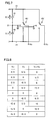
- FIG. 17 is a diagram showing a configuration of a semiconductor switch included in a conventional DC voltage converter.
- FIG. 18 is a diagram showing a switching pattern of IGBT elements Q 1 D to Q 4 D in FIG. 3 and a voltage applied to a reactor 22 .
- FIG. 19 is a diagram showing a state that a power conversion apparatus according to the present invention is applied to a three-phase, four-wire system.
- FIG. 1 is a schematic block diagram showing a main circuit configuration of an uninterruptible power supply system 100 according to an embodiment of the present invention.
- uninterruptible power supply system 100 includes an input filter 2 , a converter 3 , an inverter 4 , an output filter 5 , a DC voltage converter (denoted as “DC/DC” in the drawing) 7 , a control device 10 , a DC positive bus 13 , a DC negative bus 14 , capacitors 15 and 16 , a DC neutral point bus 17 , voltage sensors 31 and 36 , current sensors 32 and 37 , a power failure detection circuit 33 , an R-phase line RL, an S-phase line SL, and a T-phase line TL.
- DC/DC DC voltage converter
- Input filter 2 prevents leakage of harmonics to commercial AC power supply 1 .
- Commercial AC power supply 1 is a three-phase AC power supply.
- Input filter 2 is a three-phase LC filter circuit constituted of a capacitor 11 (capacitors 11 R, 115 and 11 T) and a reactor 12 (reactors 12 R, 12 S and 12 T).
- Converter 3 converts three-phase AC power supplied from commercial AC power supply 1 through input filter 2 into DC power and supplies the DC power to inverter 4 through DC positive bus 13 and DC negative bus 14 .
- Inverter 4 converts the DC power from converter 3 into three-phase AC power.
- converter 3 and inverter 4 are each implemented by a three-level circuit. Converter 3 and inverter 4 are connected to each other through DC positive bus 13 , DC negative bus 14 and DC neutral point bus 17 .
- Capacitors 15 and 16 are connected in series between DC positive bus 13 and DC negative bus 14 and they smoothen a voltage across DC positive bus 13 and DC negative bus 14 .
- DC neutral point bus 17 is connected to a neutral point 21 which is a point of connection between capacitors 15 and 16 .
- Output filter 5 removes harmonics generated by an operation of inverter 4 .
- Output filter 5 is a three-phase LC filter circuit constituted of a reactor 18 (reactors 18 U, 18 V and 18 W) and a capacitor 19 (capacitors 19 U, 19 V and 19 W).
- DC voltage converter 7 carries out conversion between a DC voltage across DC positive bus 13 and DC negative bus 14 and a voltage of a storage battery 8 . It is noted that a power storage device that can be charged and can discharge should only be connected to DC voltage converter 7 , and for example, an electric double layer capacitor may be connected to DC voltage converter 7 . In addition, though storage battery 8 is installed outside uninterruptible power supply system 100 in the present embodiment, storage battery 8 may be contained in uninterruptible power supply system 100 .
- Voltage sensor 31 detects a voltage VR of the R-phase line, a voltage VS of the S-phase line, and a voltage VT of the T-phase line, and outputs three-phase voltage signals indicating respective voltages VR, VS and VT to control device 10 and power failure detection circuit 33 .
- Current sensor 32 detects a current IR of the R-phase line, a current IS of the S-phase line, and a current IT of the T-phase line and outputs three-phase current signals indicating respective voltages IR, IS and IT to control device 10 .
- Power failure detection circuit 33 detects power failure of commercial AC power supply 1 based on the three-phase voltage signal from voltage sensor 31 . Power failure detection circuit 33 outputs a power failure signal indicating power failure of commercial AC power supply 1 to control device 10 .
- Voltage sensor 36 detects a voltage VB across positive and negative electrodes of storage battery 8 and outputs a signal indicating voltage VB to control device 10 .
- Current sensor 37 detects a current IB input and output to/from storage battery 8 and outputs a signal indicating current IB to control device 10 .
- Control device 10 controls operations of converter 3 , inverter 4 and DC voltage converter 7 .
- each of converter 3 , inverter 4 and DC voltage converter 7 is implemented by a semiconductor switch including a semiconductor switching element.
- an IGBT Insulated Gate Bipolar Transistor
- PWM Pulse Width Modulation
- Control device 10 carries out PWM control, upon receiving the three-phase voltage signal from voltage sensor 31 , the three-phase current signal from current sensor 32 , the power failure signal from power failure detection circuit 33 , the signal indicating voltage VB detected by voltage sensor 36 , the signal indicating current IB detected by current sensor 37 , and the like.
- uninterruptible power supply system 100 While commercial AC power supply 1 can normally supply AC power, converter 3 converts AC power from commercial AC power supply 1 to DC power and inverter 4 converts the DC power into AC power and supplies the AC power to load 6 .
- DC voltage converter 7 converts the DC voltage from converter 3 into a voltage suitable for charging storage battery 8 , so that storage battery 8 is charged.
- control device 10 stops converter 3 based on the power failure signal from power failure detection circuit 33 .
- control device 10 operates DC voltage converter 7 such that DC power is supplied from storage battery 8 to inverter 4 , thus causing inverter 4 to continue supply of AC power.
- DC voltage converter 7 converts the voltage of storage battery 8 into a voltage suitable as an input voltage for inverter 4 .
- AC power can be supplied to an AC load in a stable manner.
- FIG. 2 is a circuit diagram illustrating in detail a configuration of converter 3 and inverter 4 shown in FIG. 1 .
- converter 3 includes an R-phase arm 3 R, an S-phase arm 3 S and a T-phase arm 3 T.
- Inverter 4 includes a U-phase arm 4 U, a V-phase arm 4 V and a W-phase arm 4 W.
- each phase ( 3 R, 3 S, 3 T) of converter 3 and the arm of each phase ( 4 U, 4 V, 4 W) of inverter 4 are each implemented by a three-level circuit, and each of them includes four IGBT elements and six diodes.
- R-phase arm 3 R includes IGBT elements Q 1 R to Q 4 R and diodes D 1 R to D 6 R.
- S-phase arm 3 S includes IGBT elements Q 1 S to Q 4 S and diodes D 1 S to D 6 S.
- T-phase arm 3 T includes IGBT elements Q 1 T to Q 4 T and diodes D 1 T to D 6 T.
- U-phase arm 4 U includes IGBT elements Q 1 U to Q 4 U and diodes D 1 U to D 6 U.
- V-phase arm 4 V includes IGBT elements Q 1 V to Q 4 V and diodes D 1 V to D 6 V.
- W-phase arm 4 W includes IGBT elements Q 1 W to Q 4 W and diodes D 1 W to D 6 W
- reference characters R, S, T, U, V, and W are collectively denoted as a reference character “x”.
- IGBT elements Q 1 x to Q 4 x are connected in series between DC positive bus 13 and DC negative bus 14 .
- Diodes D 1 x to D 4 x are connected in anti-parallel to IGBT elements Q 1 x to Q 4 x respectively.
- Diode D 5 x is connected to a point of connection between IGBT elements Q 1 x and Q 2 x and neutral point 21 .
- Diode D 6 x is connected to a point of connection between IGBT elements Q 3 x and Q 4 x and neutral point 21 . It is noted that diode D 5 x has a cathode connected to the point of connection between IGBT elements Q 1 x and Q 2 x and has an anode connected to neutral point 21 . Diode D 6 x has an anode connected to the point of connection between IGBT elements Q 3 x and Q 4 x and has a cathode connected to neutral point 21 . Diodes D 1 x to D 4 x function as free-wheeling diodes, and diodes D 5 x and D 6 x function as clamp diodes.
- a point of connection between IGBT elements Q 2 x and Q 3 x corresponds to an AC input terminal
- a point of connection between diodes D 5 x and D 6 x corresponds to a DC output terminal.
- the point of connection between diodes D 5 x and D 6 x corresponds to a DC input terminal
- the point of connection between IGBT elements Q 2 x and Q 3 x corresponds to an AC output terminal.
- the AC input terminal of the arm of each phase ( 3 R, 3 S, 3 T) of converter 3 is connected to a corresponding line (R-phase line RL, S-phase line SL, T-phase line TL), and the AC output terminal of the arm of each phase ( 4 U, 4 V, 4 S) of inverter 4 is connected to a corresponding line (U-phase line UL, V-phase line VL, W-phase line WL).
- the DC output terminal of the arm of each phase of converter 3 and the DC input terminal of the arm of each phase of inverter 4 are connected to neutral point 21 .
- FIG. 3 is a diagram illustrating in detail a configuration of DC voltage converter 7 shown in FIG. 1 .
- DC voltage converter 7 includes a reactor 22 and a semiconductor switch 23 .
- Semiconductor switch 23 includes IGBT elements Q 1 D to Q 4 D connected in series between DC positive bus 13 and DC negative bus 14 and diodes D 1 D to D 4 D connected in anti-parallel to IGBT elements Q 1 D to Q 4 D respectively.
- one end of a reactor 22 P is connected to a point of connection between IGBT elements Q 1 D and Q 2 D and one end of a reactor 22 N is connected to a point of connection between IGBT elements Q 3 D and Q 4 D.
- the other end of reactor 22 P is connected to the positive electrode of storage battery 8 and the other end of reactor 22 N is connected to the negative electrode of storage battery 8 .
- converter 3 and inverter 4 are each implemented by a three-level circuit.
- an inverter is generally implemented by a two-level circuit. By implementing the inverter with a three-level circuit, harmonics can be suppressed more than in the conventional power conversion apparatus.
- FIG. 4 is a diagram showing a single-phase inverter implemented by a two-level circuit.
- an inverter 41 includes a U-phase arm 41 U and a V-phase arm 41 V.
- U-phase arm 41 U and V-phase arm 41 V are connected in parallel between a DC positive bus 42 and a DC negative bus 43 and they are identical in configuration.
- U-phase arm 41 U includes IGBT elements QA and QB connected in series between DC positive bus 42 and DC negative bus 43 and diodes DA and DB connected in anti-parallel to IGBT elements QA and QB respectively.
- U-phase line UL is connected to a point of connection between IGBT elements QA and QB.
- V-phase arm 41 V has such a configuration that U-phase line UL in the configuration of U-phase arm 41 U above is replaced with V-phase line VL.
- Capacitors CA and CB are connected in series between DC positive bus 42 and DC negative bus 43 .
- a neutral point O is a point of connection between capacitors CA and CB.
- a voltage across opposing ends of capacitor CA and a voltage across opposing ends of capacitor CB are both E/2 (E being a prescribed value).
- FIG. 5 is an equivalent circuit of inverter 41 shown in FIG. 4 .
- U-phase arm 41 U is equivalent to a switch that switches connection of U-phase line UL between DC positive bus 42 and DC negative bus 43 .
- a voltage Vu of U-phase line UL switches between E/2 and ⁇ E/2.
- a voltage Vv of V-phase line VL varies similarly to voltage Vu.
- the two-level circuit converts a DC voltage E to an AC voltage having two values (E/2, ⁇ E/2).
- FIG. 6 is a diagram showing a line voltage of inverter 41 .
- a line voltage (a difference between voltage Vu and voltage Vv) switches between E, 0, and ⁇ E.
- a minimum variation of the line voltage is equal to voltage E.
- FIG. 7 is an equivalent circuit diagram of U-phase arm 4 U and V-phase arm 4 V of inverter 4 shown in FIG. 2 .
- U-phase arm 4 U is equivalent to a switch that switches connection of U-phase line UL between DC positive bus 13 , neutral point 21 , and DC negative bus 14 .
- voltage Vu of U-phase line UL switches between E/2, 0 and ⁇ E/2.
- Voltage Vv of V-phase line VL also varies similarly to voltage Vu.
- the three-level circuit is a circuit capable of performing conversion between a DC voltage and an AC voltage having three values.
- FIG. 8 is a diagram showing a line voltage of a single-phase, three-level inverter shown in FIG. 7 .
- the line voltage (a difference between voltage Vu and voltage Vv) switches in a range of E, E/2, 0, ⁇ E/2, and ⁇ E.
- a minimum variation of the line voltage is equal to E/2.
- the three-level inverter is smaller in variation of the line voltage than the two-level inverter. Since a waveform of an output voltage of the inverter finely varies as the variation of the line voltage is smaller, the waveform can be closer to a sinusoidal wave. As the voltage waveform is closer to the sinusoidal wave, harmonics generated by the operation of the inverter can be made smaller. Therefore, harmonics can be made smaller by the three-level inverter than the two-level inverter.
- FIG. 9 is a diagram showing a result of simulation of a reactor current in an example where a filter reactor provided on an output side of a two-level inverter is set to 5% and the inverter is switched at a frequency of 10 kHz.
- FIG. 10 is a diagram showing a result of simulation of a reactor current in an example where a filter reactor provided on an output side of a two-level inverter is set to 10% and the inverter is switched at a frequency of 10 kHz. Comparing total harmonic distortion (THD) based on simulation in FIGS. 9 and 10 , THD is 6.4% when reactor inductance is set to 5%, whereas THD decreases to 3.2% by increasing reactor inductance to 10%.
- THD total harmonic distortion
- THD represents a ratio between the sum of effective values of harmonic components and effective values of fundamental waves. Smaller THD means smaller harmonic components.
- FIGS. 9 and 10 show that THD decreases by increasing reactor inductance. If reactor inductance is increased in order to make the harmonic components smaller, it is necessary, for example, to increase the number of turns of a coil, and a problem of increase in volume and weight of the reactor arises.
- FIG. 11 is a diagram showing a result of simulation of a reactor current in an example where a filter reactor provided on an output side of a three-level inverter is set to 5% and the inverter is switched at a frequency of 10 kHz.
- the three-level inverter can suppress harmonic components more than the two-level inverter provided that filter reactors are identical in inductance.
- THD was 3.2%.
- FIG. 12 is a diagram showing a frequency spectrum of a harmonic current ( FIG. 9 ) generated by the two-level inverter.
- FIG. 13 is a diagram showing a frequency spectrum of a harmonic current ( FIG. 11 ) generated by the three-level inverter.
- the three-level inverter can suppress harmonics more than the two-level inverter, regardless of a frequency. It is noted that frequency spectra in FIGS. 12 and 13 could be obtained by simulation. In simulation, a DC voltage input to the inverter was set to 500 V, a three-phase resistance load of 10 kW was adopted as a load, and an output voltage (line voltage) was set to 208 Vrms.
- harmonics generated by the inverter can be made smaller.
- the reactor can have smaller volume and weight. Therefore, according to the present embodiment, reduction in size and lighter weight of the power conversion apparatus can be achieved.
- the following effects can also be obtained by implementing an inverter with a three-level circuit.
- a storage battery or the like having large capacity is connected, as a DC power supply, to a DC capacitor on the input side of the inverter.
- fluctuation of a potential to ground becomes greater during operation of the inverter, an amount of generated noise increases due to a large stray capacitance of a DC circuit. Since variation of the output voltage becomes greater by implementing inverter 4 with a two-level inverter, fluctuation of a potential to ground also becomes greater.
- inverter 4 by implementing inverter 4 with a three-level inverter, variation of the output voltage thereof can be made smaller than in a case of a two-level inverter. As fluctuation of a potential to ground can thus be made smaller, an amount of generated noise can be decreased.
- FIG. 14 is a diagram showing a result of simulation of fluctuation of a potential to ground of the two-level inverter and fluctuation of a potential to ground of the three-level inverter.
- a DC voltage input to the inverter was set to 360 V.
- fluctuation of a potential to ground in the two-level inverter as 1 [p.u]
- fluctuation of a potential to ground in the three-level inverter is 0.5 [p.u].
- the three-level inverter can achieve smaller fluctuation of a potential to ground.
- loss in inverter 4 can be decreased.
- Loss in inverter 4 specifically refers to conduction loss (loss in each of the IGBT element and the diode when they are fed with power) and switching loss in the IGBT element.
- FIG. 15 is a diagram showing a result of simulation of loss in the two-level inverter and the three-level inverter.
- FIG. 16 is a diagram illustrating a breakdown of the loss in the two-level inverter and the three-level inverter.
- a DC input voltage was set to 600 V
- a switching frequency was set to 10 kHz
- an AC output voltage was set to 380 Vrms
- magnitude of a load was set to 275 kW.
- the IGBT element included in the two-level inverter is a 1200V-600 A product and the IGBT element included in the three-level inverter is a 600V-600 A product.
- the entire loss in the three-level inverter is equal to 83% of the entire loss in the two-level inverter, because switching loss is decreased.
- the three-level inverter is smaller in switching loss than the two-level inverter (33%), because a voltage applied to a single semiconductor switching element can be lowered in the three-level inverter as compared with the two-level inverter.
- switching loss occupies most (63%) of the entire loss.
- the three-level inverter can achieve significant decrease in the switching loss. Therefore, in the three-level inverter, though conduction loss increases as compared with the two-level inverter, the entire loss can be smaller than in the two-level inverter. By decreasing loss in the inverter, operation efficiency of the power conversion apparatus can be enhanced.
- converter 3 is also implemented by a three-level circuit, an effect the same as in inverter 4 can also be achieved by converter 3 .
- a reactor included in an input filter can be reduced in size.
- reduction in size and lighter weight of the power conversion apparatus can further be achieved.
- fluctuation of a potential to ground can be suppressed, an amount of noise generated by converter 3 can also be lowered.
- loss in converter 3 can be decreased, operation efficiency of the power conversion apparatus can be enhanced.
- common components can be used in converter 3 and inverter 4 , cost for the power conversion apparatus can be reduced.
- DC voltage converter 7 has conventionally had such a configuration that two IGBT elements QC and QD are connected in series as shown in a semiconductor switch 44 in FIG. 17 .
- ripple components in a current that flows through reactor 22 are decreased by implementing a semiconductor switch by connecting four IGBT elements in series.
- a voltage of (E ⁇ VB) is applied to a reactor 45
- IGBT element QC is ON and IGBT element QD is OFF
- a voltage of ( ⁇ VB) is applied to reactor 45
- a reactor voltage difference produced by switching is E.
- FIG. 18 shows a switching pattern of IGBT elements Q 1 D to Q 4 D and a voltage applied to reactor 22 . It can be seen from FIG. 18 that a voltage that can be applied to reactor 22 by DC voltage converter 7 also has three levels. According to the configuration in FIG. 3 , the reactor voltage difference produced by switching can be set to E/2 and ripple components in a current that flows through reactor 22 can be decreased. Thus, inductance of reactor 22 can be decreased and reactor 22 can be reduced in size, and therefore reduction in size and lighter weight of the power conversion apparatus can further be achieved.
- a three-level circuit has been shown, however, a circuit implementing an inverter, a converter or a DC voltage converter should only be a circuit (a multi-level circuit) that performs conversion between a DC voltage and an AC voltage or a DC voltage having at least three voltage values. Therefore, a five-level circuit for performing conversion between a DC voltage and an AC voltage having at least five voltage values is applicable to an inverter or the like.
- an uninterruptible power supply system applicable to a three-phase, three-wire system AC power supply and load has been shown, however, the present invention is also applicable to a three-phase, four-wire system AC power supply and load.
- the present invention is also applicable to a three-phase, four-wire system AC power supply and load.
- the AC power supply and the AC load are not limited to those of three phases, and a single-phase power supply or load may be adopted. In that case, two multi-level circuits should only be included in each of a converter and an inverter.
- a DC voltage converter is applied between the storage battery and the DC bus, however, the DC voltage converter can naturally be eliminated so long as the storage battery within a rated operation range of the DC bus can be selected.
- a filter achieving smaller size and lighter weight that includes a multi-level circuit as well as achieving suppression of fluctuation of a potential to ground is applicable to a power conversion apparatus outputting AC power based on DC power, such as a solar power generation system, a fuel cell power generation system, or a secondary battery energy storage system.
Landscapes
- Engineering & Computer Science (AREA)
- Power Engineering (AREA)
- Business, Economics & Management (AREA)
- Emergency Management (AREA)
- Inverter Devices (AREA)
- Stand-By Power Supply Arrangements (AREA)
Applications Claiming Priority (1)
| Application Number | Priority Date | Filing Date | Title |
|---|---|---|---|
| PCT/JP2008/063664 WO2010013322A1 (fr) | 2008-07-30 | 2008-07-30 | Dispositif de conversion d’énergie |
Publications (2)
| Publication Number | Publication Date |
|---|---|
| US20110127837A1 US20110127837A1 (en) | 2011-06-02 |
| US8994216B2 true US8994216B2 (en) | 2015-03-31 |
Family
ID=41610046
Family Applications (1)
| Application Number | Title | Priority Date | Filing Date |
|---|---|---|---|
| US13/055,373 Active 2030-07-02 US8994216B2 (en) | 2008-07-30 | 2008-07-30 | Power conversion apparatus |
Country Status (7)
| Country | Link |
|---|---|
| US (1) | US8994216B2 (fr) |
| JP (1) | JP5248611B2 (fr) |
| KR (1) | KR101189428B1 (fr) |
| CN (1) | CN102124625B (fr) |
| CA (1) | CA2732316C (fr) |
| MX (1) | MX2011000429A (fr) |
| WO (1) | WO2010013322A1 (fr) |
Cited By (4)
| Publication number | Priority date | Publication date | Assignee | Title |
|---|---|---|---|---|
| US20150042169A1 (en) * | 2013-08-07 | 2015-02-12 | Samsung Electronics Co., Ltd. | Wireless power transmission method and apparatus for stably transmitting power to plurality of wireless power reception apparatuses |
| RU2668416C1 (ru) * | 2017-04-06 | 2018-10-01 | Федеральное государственное унитарное предприятие "Крыловский государственный научный центр" | Трехуровневый преобразователь частоты |
| RU2682164C1 (ru) * | 2018-04-02 | 2019-03-15 | Федеральное государственное бюджетное образовательное учреждение высшего образования "Магнитогорский государственный технический университет им. Г.И. Носова" | Устройство управления высоковольтным преобразователем частоты |
| US11228258B2 (en) * | 2018-11-20 | 2022-01-18 | Toshiba Mitsubishi-Electric Industrial Systems Corporation | Uninterruptible power supply apparatus |
Families Citing this family (29)
| Publication number | Priority date | Publication date | Assignee | Title |
|---|---|---|---|---|
| CN102549879B (zh) | 2009-09-25 | 2014-09-03 | 东芝三菱电机产业系统株式会社 | 不间断供电电源装置 |
| KR101314886B1 (ko) | 2009-09-30 | 2013-10-04 | 도시바 미쓰비시덴키 산교시스템 가부시키가이샤 | 전력 변환 시스템 |
| WO2012025978A1 (fr) | 2010-08-23 | 2012-03-01 | 東芝三菱電機産業システム株式会社 | Dispositif de conversion d'électricité |
| JP5653458B2 (ja) | 2011-01-07 | 2015-01-14 | 東芝三菱電機産業システム株式会社 | 電力変換装置 |
| EP2512000B1 (fr) | 2011-04-15 | 2022-03-02 | ABB Schweiz AG | Systèmes et convertisseurs de puissance reconfigurables |
| CN102832796A (zh) * | 2011-06-15 | 2012-12-19 | 力博特公司 | 缓冲电路和具有该缓冲电路的逆变器 |
| AU2012340729B2 (en) | 2011-11-21 | 2017-04-06 | Zinniatek Limited | Single phase inverters cooperatively controlled to provide one, two, or three phase unipolar electricity |
| CN103138595B (zh) * | 2011-11-22 | 2016-05-25 | 通用电气公司 | 中点箝位式变流器的控制系统及控制方法 |
| DE112012005842T5 (de) * | 2012-02-08 | 2014-11-06 | Mitsubishi Electric Corporation | Energie-Umwandlungsvorrichtung |
| KR102085816B1 (ko) * | 2013-07-02 | 2020-03-06 | 엘지이노텍 주식회사 | 전력변환장치 및 에너지 저장 시스템 |
| KR102068177B1 (ko) * | 2013-09-11 | 2020-01-20 | 엘지전자 주식회사 | 에너지 저장장치, 및 이를 구비하는 전력 공급 시스템 |
| US10008917B2 (en) * | 2013-12-18 | 2018-06-26 | Otis Elevator Company | Bus capacitor bank configuration for a multi-level regenerative drive |
| US9590521B2 (en) * | 2014-07-28 | 2017-03-07 | Hamilton Sundstrand Corporation | Power converters for aircraft starter/generators |
| KR102270104B1 (ko) * | 2014-08-14 | 2021-06-25 | 엘지전자 주식회사 | 에너지 저장장치 및 이를 구비하는 에너지 저장 시스템 |
| WO2017134293A1 (fr) * | 2016-02-05 | 2017-08-10 | Abb Schweiz Ag | Modules ups et conditionnement de puissance |
| US10574086B2 (en) * | 2016-04-08 | 2020-02-25 | Rhombus Energy Solutions, Inc. | Nonlinear control algorithm and system for a single-phase AC-AC converter with bidirectional isolated DC-DC converter |
| US10951126B2 (en) * | 2016-09-22 | 2021-03-16 | Sew-Eurodrive Gmbh & Co. Kg | System and method for operating a system |
| JP6718019B2 (ja) * | 2017-04-25 | 2020-07-08 | 東芝三菱電機産業システム株式会社 | 電源装置 |
| CN107863893A (zh) * | 2017-12-14 | 2018-03-30 | 中机国际工程设计研究院有限责任公司 | 中点自平衡三电平整流系统 |
| JP6932251B2 (ja) * | 2018-04-27 | 2021-09-08 | 東芝三菱電機産業システム株式会社 | 3レベル電力変換装置、3レベル電力変換装置の制御方法、及び記憶媒体 |
| CN108696149A (zh) * | 2018-05-25 | 2018-10-23 | 中车青岛四方车辆研究所有限公司 | 牵引变流器及其控制、故障处理和载波移相方法 |
| US11601575B2 (en) | 2018-09-14 | 2023-03-07 | Gopro, Inc. | Electrical connectivity between detachable components |
| US10439512B1 (en) * | 2018-09-27 | 2019-10-08 | Schneider Electric It Corporation | Clamp circuit to reduce overshoot in power converters |
| EP3883115A4 (fr) * | 2018-11-14 | 2022-06-22 | Toshiba Mitsubishi-Electric Industrial Systems Corporation | Dispositif de conversion de courant |
| WO2020245916A1 (fr) * | 2019-06-04 | 2020-12-10 | 東芝三菱電機産業システム株式会社 | Dispositif de conversion de puissance et dispositif de commande de conversion de puissance |
| US11909305B2 (en) * | 2019-08-30 | 2024-02-20 | Mitsubishi Electric Corporation | AC-to-DC power converter which removed a common mode component form the output current |
| US11303149B2 (en) * | 2020-02-03 | 2022-04-12 | Schneider Electric It Corporation | Short-circuit current capacity enhancement |
| CN114069819A (zh) * | 2020-08-07 | 2022-02-18 | 台达电子工业股份有限公司 | 具有三阶层切换电路的转换装置及三阶层切换电路的操作方法 |
| CN112152497B (zh) * | 2020-10-09 | 2021-07-02 | 上海海事大学 | 一种级联型五电平逆变器的容错控制方法 |
Citations (29)
| Publication number | Priority date | Publication date | Assignee | Title |
|---|---|---|---|---|
| JPS56121374A (en) | 1980-02-26 | 1981-09-24 | Toshiba Corp | Inverter device |
| JPH0833233A (ja) | 1994-07-15 | 1996-02-02 | Sanyo Denki Co Ltd | 交直流無停電電源装置 |
| US5638266A (en) * | 1994-03-10 | 1997-06-10 | Hitachi, Ltd. | Free wheel diode arrangement for neutral point clamped electric power conversion apparatus |
| US5892674A (en) * | 1996-02-16 | 1999-04-06 | Hitachi, Ltd. | Method and apparatus for power converting AC into DC or DC into AC by converter having common phase connection |
| WO1999060690A1 (fr) | 1998-05-21 | 1999-11-25 | Powerware Corporation | Systemes et procedes permettant d'assurer une alimentation de secours sans interruption pour des charges en courant alternatif au moyen d'un courant alternatif redresse et d'une pile |
| CA2314782A1 (fr) | 1999-08-13 | 2001-02-13 | Powerware Corporation | Convertisseurs d'alimentation multimode comportant des circuits d'equilibrage et methode de fonctionnement desdits appareils |
| JP2002247862A (ja) | 2001-02-20 | 2002-08-30 | Hitachi Ltd | 電力変換装置 |
| JP2002369542A (ja) | 2001-06-12 | 2002-12-20 | Mitsubishi Electric Corp | 半導体パワーモジュールおよび電力変換装置 |
| JP2003299365A (ja) | 2002-04-01 | 2003-10-17 | Fuji Electric Co Ltd | インバータ回路 |
| JP2004248479A (ja) | 2003-02-17 | 2004-09-02 | Toshiba Corp | 3レベルコンバータ |
| JP2004350471A (ja) | 2003-05-26 | 2004-12-09 | Hitachi Medical Corp | 電圧分圧回路 |
| CN1635695A (zh) | 2003-12-26 | 2005-07-06 | 台达电子工业股份有限公司 | 具有电压钳位电路的直流/直流变换器 |
| JP2005333775A (ja) | 2004-05-21 | 2005-12-02 | Sanken Electric Co Ltd | 交流電源装置 |
| JP2006109603A (ja) | 2004-10-05 | 2006-04-20 | Densei Lambda Kk | 無停電電源装置、無停電電源装置の制御方法、無停電電源システム、および、無停電電源用プログラム |
| JP2006141165A (ja) | 2004-11-15 | 2006-06-01 | Fuji Electric Systems Co Ltd | 無停電電源装置 |
| JP2006238514A (ja) | 2005-02-22 | 2006-09-07 | Hitachi Ltd | 無停電電源装置 |
| JP2006345647A (ja) | 2005-06-09 | 2006-12-21 | Fuji Electric Systems Co Ltd | 無停電電源装置 |
| JP2007028860A (ja) | 2005-07-21 | 2007-02-01 | Hitachi Ltd | 電力変換装置及びこれを備えた鉄道車輌 |
| JP2007089301A (ja) | 2005-09-21 | 2007-04-05 | Nec Fielding Ltd | 無停電電源装置及び無停電電源装置の出力制御方法 |
| CN2901688Y (zh) | 2006-05-25 | 2007-05-16 | 山东新风光电子科技发展有限公司 | 一种电流源的逆变电路 |
| JP2007151231A (ja) | 2005-11-24 | 2007-06-14 | Toshiba Mitsubishi-Electric Industrial System Corp | 無停電電源装置 |
| JP2007215344A (ja) | 2006-02-10 | 2007-08-23 | Meidensha Corp | 無停電電源システム |
| JP2007215378A (ja) | 2006-02-13 | 2007-08-23 | Fuji Electric Systems Co Ltd | 無停電電源装置 |
| JP2007300712A (ja) | 2006-04-28 | 2007-11-15 | Sanken Electric Co Ltd | 交流電力供給装置 |
| JP2008022625A (ja) | 2006-07-12 | 2008-01-31 | Fuji Electric Systems Co Ltd | 交流−直流変換装置 |
| JP2008141850A (ja) | 2006-11-30 | 2008-06-19 | Hitachi Ltd | 無停電電源システム、インバータ回路、及びリアクトル盤 |
| JP2008193779A (ja) | 2007-02-02 | 2008-08-21 | Fuji Electric Systems Co Ltd | 半導体モジュール |
| US20080238383A1 (en) * | 2007-03-19 | 2008-10-02 | Honda Motor Co., Ltd. | Power converter and multiport power converter |
| US20090284200A1 (en) | 2008-05-13 | 2009-11-19 | Fuji Electric Device Technology Co., Ltd. | AC motor driving circuit and electric vehicle driving circuit |
-
2008
- 2008-07-30 WO PCT/JP2008/063664 patent/WO2010013322A1/fr active Application Filing
- 2008-07-30 US US13/055,373 patent/US8994216B2/en active Active
- 2008-07-30 JP JP2010522555A patent/JP5248611B2/ja active Active
- 2008-07-30 KR KR1020107029347A patent/KR101189428B1/ko active IP Right Grant
- 2008-07-30 CN CN200880130518.XA patent/CN102124625B/zh active Active
- 2008-07-30 MX MX2011000429A patent/MX2011000429A/es active IP Right Grant
- 2008-07-30 CA CA 2732316 patent/CA2732316C/fr active Active
Patent Citations (32)
| Publication number | Priority date | Publication date | Assignee | Title |
|---|---|---|---|---|
| JPS56121374A (en) | 1980-02-26 | 1981-09-24 | Toshiba Corp | Inverter device |
| US5638266A (en) * | 1994-03-10 | 1997-06-10 | Hitachi, Ltd. | Free wheel diode arrangement for neutral point clamped electric power conversion apparatus |
| JPH0833233A (ja) | 1994-07-15 | 1996-02-02 | Sanyo Denki Co Ltd | 交直流無停電電源装置 |
| US5892674A (en) * | 1996-02-16 | 1999-04-06 | Hitachi, Ltd. | Method and apparatus for power converting AC into DC or DC into AC by converter having common phase connection |
| WO1999060690A1 (fr) | 1998-05-21 | 1999-11-25 | Powerware Corporation | Systemes et procedes permettant d'assurer une alimentation de secours sans interruption pour des charges en courant alternatif au moyen d'un courant alternatif redresse et d'une pile |
| JP2002516558A (ja) | 1998-05-21 | 2002-06-04 | パワーウェア・コーポレーション | 整流されたac及び蓄電池を用いてac負荷用スタンドバイ無停電電力を生成するシステム及び方法 |
| CA2314782A1 (fr) | 1999-08-13 | 2001-02-13 | Powerware Corporation | Convertisseurs d'alimentation multimode comportant des circuits d'equilibrage et methode de fonctionnement desdits appareils |
| JP2002247862A (ja) | 2001-02-20 | 2002-08-30 | Hitachi Ltd | 電力変換装置 |
| JP2002369542A (ja) | 2001-06-12 | 2002-12-20 | Mitsubishi Electric Corp | 半導体パワーモジュールおよび電力変換装置 |
| JP2003299365A (ja) | 2002-04-01 | 2003-10-17 | Fuji Electric Co Ltd | インバータ回路 |
| JP2004248479A (ja) | 2003-02-17 | 2004-09-02 | Toshiba Corp | 3レベルコンバータ |
| JP2004350471A (ja) | 2003-05-26 | 2004-12-09 | Hitachi Medical Corp | 電圧分圧回路 |
| CN1635695A (zh) | 2003-12-26 | 2005-07-06 | 台达电子工业股份有限公司 | 具有电压钳位电路的直流/直流变换器 |
| JP2005333775A (ja) | 2004-05-21 | 2005-12-02 | Sanken Electric Co Ltd | 交流電源装置 |
| JP2006109603A (ja) | 2004-10-05 | 2006-04-20 | Densei Lambda Kk | 無停電電源装置、無停電電源装置の制御方法、無停電電源システム、および、無停電電源用プログラム |
| JP2006141165A (ja) | 2004-11-15 | 2006-06-01 | Fuji Electric Systems Co Ltd | 無停電電源装置 |
| JP2006238514A (ja) | 2005-02-22 | 2006-09-07 | Hitachi Ltd | 無停電電源装置 |
| JP2006345647A (ja) | 2005-06-09 | 2006-12-21 | Fuji Electric Systems Co Ltd | 無停電電源装置 |
| JP2007028860A (ja) | 2005-07-21 | 2007-02-01 | Hitachi Ltd | 電力変換装置及びこれを備えた鉄道車輌 |
| JP2007089301A (ja) | 2005-09-21 | 2007-04-05 | Nec Fielding Ltd | 無停電電源装置及び無停電電源装置の出力制御方法 |
| JP2007151231A (ja) | 2005-11-24 | 2007-06-14 | Toshiba Mitsubishi-Electric Industrial System Corp | 無停電電源装置 |
| JP2007215344A (ja) | 2006-02-10 | 2007-08-23 | Meidensha Corp | 無停電電源システム |
| JP2007215378A (ja) | 2006-02-13 | 2007-08-23 | Fuji Electric Systems Co Ltd | 無停電電源装置 |
| JP2007300712A (ja) | 2006-04-28 | 2007-11-15 | Sanken Electric Co Ltd | 交流電力供給装置 |
| CN2901688Y (zh) | 2006-05-25 | 2007-05-16 | 山东新风光电子科技发展有限公司 | 一种电流源的逆变电路 |
| JP2008022625A (ja) | 2006-07-12 | 2008-01-31 | Fuji Electric Systems Co Ltd | 交流−直流変換装置 |
| JP2008141850A (ja) | 2006-11-30 | 2008-06-19 | Hitachi Ltd | 無停電電源システム、インバータ回路、及びリアクトル盤 |
| JP2008193779A (ja) | 2007-02-02 | 2008-08-21 | Fuji Electric Systems Co Ltd | 半導体モジュール |
| US20100039843A1 (en) | 2007-02-02 | 2010-02-18 | Fuji Electric Systems Co., Ltd | Semiconductor module for use in power supply |
| US20080238383A1 (en) * | 2007-03-19 | 2008-10-02 | Honda Motor Co., Ltd. | Power converter and multiport power converter |
| US20090284200A1 (en) | 2008-05-13 | 2009-11-19 | Fuji Electric Device Technology Co., Ltd. | AC motor driving circuit and electric vehicle driving circuit |
| JP2009278732A (ja) | 2008-05-13 | 2009-11-26 | Fuji Electric Device Technology Co Ltd | 交流電動機駆動回路及び電気車駆動回路 |
Non-Patent Citations (8)
| Title |
|---|
| Combined Office Action and Search Report issued Jul. 23, 2014 in Chinese Patent Application No. 200880130518.X (with English translation and English translation of Category of Cited Documents). |
| Combined Office Action and Search Report issued Nov. 14, 2012 in Chinese Application No. 200880130518.X (With English Translation). |
| International Search Report issued Sep. 2, 2008 in PCT/JP08/63664 filed Jul. 30, 2008. |
| Office Action issued Jan. 11, 2012 in Korea Application No. 10-2010-7029347 (With English Translation). |
| U.S. Appl. No. 13/057,102, filed Feb. 1, 2011, Sato, et al. |
| U.S. Appl. No. 13/498,009, filed Mar. 23, 2012, Sato, et al. |
| U.S. Appl. No. 13/498,515, filed Mar. 27, 2012, Sato, et al. |
| U.S. Appl. No. 13/879,937, filed Apr. 17, 2013, Kinoshita. |
Cited By (5)
| Publication number | Priority date | Publication date | Assignee | Title |
|---|---|---|---|---|
| US20150042169A1 (en) * | 2013-08-07 | 2015-02-12 | Samsung Electronics Co., Ltd. | Wireless power transmission method and apparatus for stably transmitting power to plurality of wireless power reception apparatuses |
| US9796281B2 (en) * | 2013-08-07 | 2017-10-24 | Samsung Electronics Co., Ltd. | Wireless power transmission method and apparatus for stably transmitting power to plurality of wireless power reception apparatuses |
| RU2668416C1 (ru) * | 2017-04-06 | 2018-10-01 | Федеральное государственное унитарное предприятие "Крыловский государственный научный центр" | Трехуровневый преобразователь частоты |
| RU2682164C1 (ru) * | 2018-04-02 | 2019-03-15 | Федеральное государственное бюджетное образовательное учреждение высшего образования "Магнитогорский государственный технический университет им. Г.И. Носова" | Устройство управления высоковольтным преобразователем частоты |
| US11228258B2 (en) * | 2018-11-20 | 2022-01-18 | Toshiba Mitsubishi-Electric Industrial Systems Corporation | Uninterruptible power supply apparatus |
Also Published As
| Publication number | Publication date |
|---|---|
| CA2732316A1 (fr) | 2010-02-04 |
| JPWO2010013322A1 (ja) | 2012-01-05 |
| KR101189428B1 (ko) | 2012-10-10 |
| KR20110028304A (ko) | 2011-03-17 |
| JP5248611B2 (ja) | 2013-07-31 |
| CA2732316C (fr) | 2015-01-06 |
| MX2011000429A (es) | 2011-02-23 |
| US20110127837A1 (en) | 2011-06-02 |
| WO2010013322A1 (fr) | 2010-02-04 |
| CN102124625B (zh) | 2015-11-25 |
| WO2010013322A9 (fr) | 2010-12-02 |
| CN102124625A (zh) | 2011-07-13 |
Similar Documents
| Publication | Publication Date | Title |
|---|---|---|
| US8994216B2 (en) | Power conversion apparatus | |
| US8508957B2 (en) | Power conversion device for converting DC power to AC power | |
| US8400792B2 (en) | Power conversion apparatus | |
| US10892682B2 (en) | Power converter with controllable DC offset | |
| JP6227041B2 (ja) | マルチレベルインバータ | |
| US9450502B2 (en) | Direct power conversion device and method for controlling direct power conversion device | |
| US20090244936A1 (en) | Three-phase inverter | |
| JP4783294B2 (ja) | 系統連系用電力変換装置 | |
| US8207712B2 (en) | Arrangement for exchanging power | |
| US11228258B2 (en) | Uninterruptible power supply apparatus | |
| WO2010095241A1 (fr) | Convertisseur de puissance | |
| US8493760B2 (en) | Electric circuit for converting direct current into alternating current |
Legal Events
| Date | Code | Title | Description |
|---|---|---|---|
| AS | Assignment |
Owner name: TOSHIBA MITSUBISHI-ELECTRIC INDUSTRIAL SYSTEMS COR Free format text: ASSIGNMENT OF ASSIGNORS INTEREST;ASSIGNORS:SATO, EDUARDO KAZUHIDE;KINOSHITA, MASAHIRO;YAMAMOTO, YUSHIN;AND OTHERS;SIGNING DATES FROM 20101102 TO 20101119;REEL/FRAME:025721/0240 |
|
| STCF | Information on status: patent grant |
Free format text: PATENTED CASE |
|
| MAFP | Maintenance fee payment |
Free format text: PAYMENT OF MAINTENANCE FEE, 4TH YEAR, LARGE ENTITY (ORIGINAL EVENT CODE: M1551); ENTITY STATUS OF PATENT OWNER: LARGE ENTITY Year of fee payment: 4 |
|
| MAFP | Maintenance fee payment |
Free format text: PAYMENT OF MAINTENANCE FEE, 8TH YEAR, LARGE ENTITY (ORIGINAL EVENT CODE: M1552); ENTITY STATUS OF PATENT OWNER: LARGE ENTITY Year of fee payment: 8 |
|
| AS | Assignment |
Owner name: TMEIC CORPORATION, JAPAN Free format text: CHANGE OF NAME;ASSIGNOR:TOSHIBA MITSUBISHI-ELECTRIC INDUSTRIAL SYSTEMS CORPORATION;REEL/FRAME:067244/0359 Effective date: 20240401 |