US8828247B2 - Method of manufacturing printed circuit board having vias and fine circuit and printed circuit board manufactured using the same - Google Patents
Method of manufacturing printed circuit board having vias and fine circuit and printed circuit board manufactured using the same Download PDFInfo
- Publication number
- US8828247B2 US8828247B2 US13/589,635 US201213589635A US8828247B2 US 8828247 B2 US8828247 B2 US 8828247B2 US 201213589635 A US201213589635 A US 201213589635A US 8828247 B2 US8828247 B2 US 8828247B2
- Authority
- US
- United States
- Prior art keywords
- substrate
- circuit pattern
- layer
- photosensitive resist
- etching
- Prior art date
- Legal status (The legal status is an assumption and is not a legal conclusion. Google has not performed a legal analysis and makes no representation as to the accuracy of the status listed.)
- Active
Links
Images


Classifications
-
- H—ELECTRICITY
- H05—ELECTRIC TECHNIQUES NOT OTHERWISE PROVIDED FOR
- H05K—PRINTED CIRCUITS; CASINGS OR CONSTRUCTIONAL DETAILS OF ELECTRIC APPARATUS; MANUFACTURE OF ASSEMBLAGES OF ELECTRICAL COMPONENTS
- H05K3/00—Apparatus or processes for manufacturing printed circuits
- H05K3/46—Manufacturing multilayer circuits
-
- H—ELECTRICITY
- H05—ELECTRIC TECHNIQUES NOT OTHERWISE PROVIDED FOR
- H05K—PRINTED CIRCUITS; CASINGS OR CONSTRUCTIONAL DETAILS OF ELECTRIC APPARATUS; MANUFACTURE OF ASSEMBLAGES OF ELECTRICAL COMPONENTS
- H05K3/00—Apparatus or processes for manufacturing printed circuits
- H05K3/02—Apparatus or processes for manufacturing printed circuits in which the conductive material is applied to the surface of the insulating support and is thereafter removed from such areas of the surface which are not intended for current conducting or shielding
- H05K3/04—Apparatus or processes for manufacturing printed circuits in which the conductive material is applied to the surface of the insulating support and is thereafter removed from such areas of the surface which are not intended for current conducting or shielding the conductive material being removed mechanically, e.g. by punching
- H05K3/045—Apparatus or processes for manufacturing printed circuits in which the conductive material is applied to the surface of the insulating support and is thereafter removed from such areas of the surface which are not intended for current conducting or shielding the conductive material being removed mechanically, e.g. by punching by making a conductive layer having a relief pattern, followed by abrading of the raised portions
-
- H—ELECTRICITY
- H05—ELECTRIC TECHNIQUES NOT OTHERWISE PROVIDED FOR
- H05K—PRINTED CIRCUITS; CASINGS OR CONSTRUCTIONAL DETAILS OF ELECTRIC APPARATUS; MANUFACTURE OF ASSEMBLAGES OF ELECTRICAL COMPONENTS
- H05K3/00—Apparatus or processes for manufacturing printed circuits
- H05K3/10—Apparatus or processes for manufacturing printed circuits in which conductive material is applied to the insulating support in such a manner as to form the desired conductive pattern
-
- H—ELECTRICITY
- H05—ELECTRIC TECHNIQUES NOT OTHERWISE PROVIDED FOR
- H05K—PRINTED CIRCUITS; CASINGS OR CONSTRUCTIONAL DETAILS OF ELECTRIC APPARATUS; MANUFACTURE OF ASSEMBLAGES OF ELECTRICAL COMPONENTS
- H05K3/00—Apparatus or processes for manufacturing printed circuits
- H05K3/40—Forming printed elements for providing electric connections to or between printed circuits
-
- H—ELECTRICITY
- H05—ELECTRIC TECHNIQUES NOT OTHERWISE PROVIDED FOR
- H05K—PRINTED CIRCUITS; CASINGS OR CONSTRUCTIONAL DETAILS OF ELECTRIC APPARATUS; MANUFACTURE OF ASSEMBLAGES OF ELECTRICAL COMPONENTS
- H05K2203/00—Indexing scheme relating to apparatus or processes for manufacturing printed circuits covered by H05K3/00
- H05K2203/02—Details related to mechanical or acoustic processing, e.g. drilling, punching, cutting, using ultrasound
- H05K2203/025—Abrading, e.g. grinding or sand blasting
-
- H—ELECTRICITY
- H05—ELECTRIC TECHNIQUES NOT OTHERWISE PROVIDED FOR
- H05K—PRINTED CIRCUITS; CASINGS OR CONSTRUCTIONAL DETAILS OF ELECTRIC APPARATUS; MANUFACTURE OF ASSEMBLAGES OF ELECTRICAL COMPONENTS
- H05K2203/00—Indexing scheme relating to apparatus or processes for manufacturing printed circuits covered by H05K3/00
- H05K2203/03—Metal processing
- H05K2203/0323—Working metal substrate or core, e.g. by etching, deforming
-
- H—ELECTRICITY
- H05—ELECTRIC TECHNIQUES NOT OTHERWISE PROVIDED FOR
- H05K—PRINTED CIRCUITS; CASINGS OR CONSTRUCTIONAL DETAILS OF ELECTRIC APPARATUS; MANUFACTURE OF ASSEMBLAGES OF ELECTRICAL COMPONENTS
- H05K2203/00—Indexing scheme relating to apparatus or processes for manufacturing printed circuits covered by H05K3/00
- H05K2203/03—Metal processing
- H05K2203/0369—Etching selective parts of a metal substrate through part of its thickness, e.g. using etch resist
-
- H—ELECTRICITY
- H05—ELECTRIC TECHNIQUES NOT OTHERWISE PROVIDED FOR
- H05K—PRINTED CIRCUITS; CASINGS OR CONSTRUCTIONAL DETAILS OF ELECTRIC APPARATUS; MANUFACTURE OF ASSEMBLAGES OF ELECTRICAL COMPONENTS
- H05K2203/00—Indexing scheme relating to apparatus or processes for manufacturing printed circuits covered by H05K3/00
- H05K2203/14—Related to the order of processing steps
- H05K2203/1476—Same or similar kind of process performed in phases, e.g. coarse patterning followed by fine patterning
-
- H—ELECTRICITY
- H05—ELECTRIC TECHNIQUES NOT OTHERWISE PROVIDED FOR
- H05K—PRINTED CIRCUITS; CASINGS OR CONSTRUCTIONAL DETAILS OF ELECTRIC APPARATUS; MANUFACTURE OF ASSEMBLAGES OF ELECTRICAL COMPONENTS
- H05K3/00—Apparatus or processes for manufacturing printed circuits
- H05K3/40—Forming printed elements for providing electric connections to or between printed circuits
- H05K3/4038—Through-connections; Vertical interconnect access [VIA] connections
Definitions
- PCB printed circuit board
- interlayer conduction vias and a fine circuit are integrally formed using a laser trench process method or an imprint method, which are disclosed in Korean Patent Registration No. 10-1109323.
- a pattern is formed (S 10 ), non-electrolytic copper plating (S 20 ) and electrolytic copper plating (S 30 ) are carried out, and a planarization process (S 40 ) is carried out to form vias and a fine circuit at a PCB.
- FIGS. 2A-2D show a related art LTP method of manufacturing a PCB having vias and a fine circuit, which are integrally formed
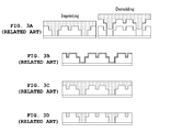
- FIGS. 3A-3D show a related art imprint method of manufacturing a PCB having vias and a fine circuit, which are integrally formed.
- a surface of a dielectric layer at which a circuit pattern is to be formed is removed using a fine circuit forming device, such as an excimer laser, to form a pattern ( FIG. 2A ), copper plating ( FIGS. 2B and 2C ) are carried out to form a metal layer, and a planarization process ( FIG. 2D ) is carried out to complete a circuit.
- a fine circuit forming device such as an excimer laser
- a circuit pattern to be formed at a substrate is formed at a mold in an embossed state, and the embossed mold is pressed against a dielectric layer of the substrate to transfer the circuit ( FIG. 3A ).
- copper plating FIGS. 3B and 3C
- a planarization process FIG. 3D
- Exemplary embodiments are provided to address the above problems and provide a method of manufacturing a PCB having vias and a fine circuit, which are integrally formed, without a Cu plating process to form an additional metal layer.
- a method of manufacturing a circuit board including: (a) providing a substrate made of a conductive material; (b) etching a first surface of the substrate excluding a region in which at least one via is to be formed; (c) etching a region of the etched first surface of the substrate in which an insulated portion of a first circuit pattern is to be formed; (d) stacking a first insulation layer in spaces formed by the etching performed in operations (b) and (c); and (e) grinding a second surface of the substrate to expose the first insulation layer outward along with the first circuit pattern, thereby forming a circuit board.
- Operation (b) may include (b1) applying a first photosensitive resist layer to the first surface of the substrate; (b2) exposing and developing the first photosensitive resist layer in which the at least one via is to be formed; and (b3) etching the first surface using the first photosensitive resist layer.
- Operation (b) may further include (b4) removing the first photosensitive resist layer.
- Operation (c) may include (c1) applying a second photosensitive resist layer to the etched first surface of the substrate; (c2) exposing and developing the second photosensitive resist layer in which the first circuit pattern is to be formed; and (c3) etching the etched first surface using the second photosensitive resist layer.
- the second photosensitive resist layer may be formed of a dry film resist (DFR) or an electric deposit photo resist (EDPR).
- DFR dry film resist
- EDPR electric deposit photo resist
- the second photosensitive resist layer may be exposed using a laser direct image (LDI).
- LDLI laser direct image
- Operation (c) may further include (c4) removing the second photosensitive resist layer.
- the first dielectric layer may be formed of a prepreg.
- the method of manufacturing the circuit board may further include (f) forming a second circuit pattern on the first surface of the substrate where the first insulation layer is stacked in the spaces formed by the etching performed in operations (b) and (c).
- the second circuit pattern may be formed using any one selected from a group consisting of a tenting process, a panel/pattern process, a semi additive process, a modified semi additive process, an advanced modified semi additive process, and a full additive process.
- Operation (f) may include fully forming a fifth photosensitive resist over the side of the substrate at which the first circuit pattern is formed when the second circuit pattern is formed.
- the circuit board and at least one another circuit board having the same structure may be bonded to form a multi layer circuit board.
- the method of manufacturing the circuit board may further include performing surface protection treatment with respect to at least one of the first surface where the first insulation layer is stacked in the spaces formed by the etching performed in operations (b) and (c), and the second surface.
- the step of performing surface protection treatment may include forming a patterned photo solder resist (PSR) protection layer to perform the surface protection treatment.
- PSR photo solder resist
- a method of manufacturing a circuit board including: (a) providing a substrate made of a conductive material; (b) etching a first surface of the substrate excluding a region in which at least one via is to be formed; (c) etching a region of the etched first surface of the substrate in which an insulated portion of a first circuit pattern is to be formed; (d) stacking a first insulation layer in spaces formed by the etching performed in operations (b) and (c); (e) stacking a first conductive layer on the first surface of the substrate after operation (d); (f) etching the first and second surfaces of the substrate after operation (e) so that the first insulation layer is exposed outward along with the first circuit pattern; and (g) forming a second circuit pattern at the first conductive layer.
- the second circuit pattern may be formed using any one selected from a group consisting of a tenting process, a panel/pattern process, a semi additive process, a modified semi additive process, an advanced modified semi additive process, and a full additive process.
- Operation (g) may include fully forming a fifth photosensitive resist on the first surface of the substrate at which the first circuit pattern is formed before the second circuit pattern is formed.
- FIG. 1 is a flow chart showing a related art method of manufacturing a PCB having vias and a fine circuit, which are integrally formed;
- FIGS. 2A-2D illustrate a related art method of manufacturing a PCB having vias and a fine circuit, which are integrally formed, based on a laser trench process (LTP);
- LTP laser trench process
- FIGS. 3A-3D illustrate a related art method of manufacturing a PCB having vias and a fine circuit, which are integrally formed, based on an imprint method
- FIGS. 4A-4I illustrate a method of manufacturing a PCB having vias and a fine circuit according to an exemplary embodiment
- FIG. 5 is a flow chart showing the method of FIG. 4 ;
- FIGS. 6A-6D illustrate a method of forming a second fine circuit of a two layer PCB having vias and a fine circuit according to another exemplary embodiment based on a subtractive method
- FIGS. 7A-7D illustrate a method of forming the second fine circuit of the PCB having the vias and the fine circuit according to another exemplary embodiment based on an additive method
- FIG. 8 is a flow chart showing the methods of FIGS. 6A-6D and 7 A- 7 D;
- FIGS. 9A-9E illustrate another embodiment of the method of FIGS. 6A-6D ;
- FIG. 10 is a flow chart showing the method of FIGS. 9A-9E ;
- FIGS. 11A-11C and 12 A- 12 C illustrate a method of manufacturing a four layer PCB having vias and a fine circuit according to a further exemplary embodiment
- FIG. 13 is a flow chart showing the methods of FIGS. 11A-11C and 12 A- 12 C.
- FIGS. 4A-4I and FIG. 5 illustrate a method of manufacturing a PCB having vias and a fine circuit according to a first exemplary embodiment.
- the method of manufacturing the PCB having the vias and the fine circuit according to the first exemplary embodiment includes operations as follows.
- a substrate made of a conductive material is provided (S 100 ).
- a first surface of the substrate excluding a region in which vias are to be formed is etched (S 200 ).
- another etching is performed on a region which is to form an insulated portion of a first fine circuit pattern (S 300 ).
- a dielectric layer is stacked in spaces formed by the selective etching in operations S 200 and S 300 (S 400 ).
- a second surface of the substrate which is opposite to the first surface, is grinded to expose the dielectric layer, stacked in spaces formed by the selective etching in operations S 200 and S 300 , outward (S 500 ).
- Surface protection treatment is performed with respect to at least one of the first surface of the substrate on which the dielectric layer is stacked and the grinded second surface of the substrate (S 600 ).
- the method of manufacturing the PCB having the vias and the fine circuit according to the first exemplary embodiment begins with providing a substrate made of a conductive material (S 100 ).
- vias and a fine circuit are formed using a substrate made of an insulative material.
- a substrate 100 made of a conductive material is used to form vias and a fine circuit. Consequently, the manufacturing method according to the first exemplary embodiment may omit a copper plating process, which is indispensable in the related art.
- the substrate 100 may be made of a conductive material, such as gold (Au), silver (Ag) or copper (Cu).
- the substrate 100 is made of Cu in terms of conductivity and productivity.
- a surface of the substrate 100 is primarily etched except a region in the surface in which vias 101 are to be formed so that the vias 101 protrude in a bulging shape and the other region in the surface is removed by etching (S 200 ).
- the primary etching operation includes applying a first photosensitive resist layer 110 to a first surface of the substrate 100 (S 210 ), exposing and developing the first photosensitive resist layer 110 corresponding to a pattern in which vias 101 are to be formed (S 220 ), primarily etching the first surface exposed outward using the first photosensitive resist layer 110 (S 230 ), and removing the remainder of the first photosensitive resist layer 110 after the primary etching (S 240 ).
- the first photosensitive resist layer 110 may be formed of a photosensitive resist, such as a dry film resist (DFR) or a liquid photo resist (LPR).
- the first photosensitive resist layer 110 is patterned by exposing the first photosensitive resist layer 110 using a mask pattern (not shown) corresponding to the pattern in which the vias 101 are to be formed or a laser direct image (LDI).
- LDLI laser direct image
- the partially exposed first photosensitive resist layer 110 is developed using a developing solution to remove a positive portion of the first photosensitive resist layer 110 , i.e.
- the first photosensitive resist layer 110 is patterned ( FIG. 4B ).
- the first photosensitive resist layer 110 is patterned, the first surface of the substrate 100 except the region in which the vias 101 are to be formed is exposed outward as one surface of the conductive substrate 100 , and the outwardly exposed portion of the conductive substrate 100 is removed by etching. As a result, the substrate 100 is structure such that only the vias 101 protrude in a bulging shape ( FIG. 4C ). Subsequently, the first photosensitive resist layer 110 is removed by peeling.
- the next operation of the manufacturing method according to the first exemplary embodiment is secondarily etching a portion of the first surface of the substrate, i.e. the primarily etched surface of the substrate 100 , corresponding to an insulated region of a first fine circuit pattern (S 300 ).
- the secondary etching operation (S 300 ) includes forming a second photosensitive resist layer 120 on the primarily etched surface of the substrate (S 310 ), exposing and developing the second photosensitive resist layer 120 corresponding to the pattern in which the first fine circuit is to be formed (S 320 ), secondary etching the first surface exposed outward through the second photosensitive resist layer 120 (S 330 ), and removing the remainder of the second photosensitive resist layer 120 after the second etching (S 340 ).
- the second photosensitive resist layer 120 is applied to the first surface of the substrate at which the vias 101 protrude by electrodeposition ( FIG. 4D ).
- the second photosensitive resist layer 120 may be formed of a photosensitive resist, such as a DFR or an LPR.
- the second photosensitive resist layer 120 may be formed of an electric deposit photo resist (EDPR).
- EDPR electric deposit photo resist
- exposure and developing processes (S 320 ) of exposing and developing the second photosensitive resist layer 120 will be individually described as follows.
- the exposure process may be carried out using a mask pattern (not shown) or using the LDI process without an additional mask.
- the LDI process is a process for irradiating a laser to a desired portion based on data stored in a computer so that the desired portion can be exposed.
- the laser may be irradiated to the portion corresponding to the first fine circuit pattern so that the portion can be exposed.
- the second photosensitive resist layer 120 is exposed using the LDI process, it is not necessary to provide an additional mask, to realize a fine circuit having high resolution at a high speed, and to prevent the occurrence of defects due to foreign matter on the mask after exposure. Consequently, it is preferable, but not necessary, to carry out exposure using the LDI process.
- a subsequent process i.e. the developing process, is carried out as follows.
- the second photosensitive resist layer 120 is developed, in the same manner as the method of forming the vias 101 using the first photosensitive resist layer 110 , to remove a positive portion of the second photosensitive resist layer 120 , i.e. a portion of the second photosensitive resist layer 120 exposed by light, or a negative portion of the second photosensitive resist layer 120 , i.e. a portion of the second photosensitive resist layer 120 not exposed by light.
- the second photosensitive resist layer 120 is patterned ( FIG. 4E ).
- a region corresponding to the insulated portion of the fine circuit pattern is exposed outward, and the exposed insulated portion of the fine circuit pattern is removed by the thickness of the fine circuit pattern at the minimum through etching. As a result, a portion corresponding to the first fine circuit pattern is formed at the substrate ( FIG. 4F ).
- the remainder of the second photosensitive resist layer 120 is also removed by peeling after the patterning of the second photosensitive resist layer 120 .
- a next operation of the manufacturing method according to the first exemplary embodiment is stacking a first dielectric layer 160 in spaces formed by the primary etching and the secondary etching (S 400 ).
- the first dielectric layer 160 is stacked in the space formed by the primary etching, which is not occupied by the vias 101 , and the space corresponding to the insulated portion of the first fine circuit pattern, which is formed by the second etching.
- the first dielectric layer 160 is stacked to the height of each of the vias at the minimum to form a coreless board (see FIG. 4G ).
- a prepreg which is formed in a half-hardened state by infiltrating a thermally curable resin into a glass fiber, as the first dielectric layer 160 in terms of heat resistance, copper film adhesion and high dielectric constant.
- a next operation of the manufacturing method according to the first exemplary embodiment is grinding the second surface of the substrate 100 to expose the insulated portion of the first fine circuit pattern formed by the first dielectric layer 160 outward (S 500 ).
- the second surface of the substrate 100 which is opposite to the first surface at which the first dielectric layer 160 is stacked, is fully etched.
- a planarization process may be carried out through chemical mechanical polishing or various mechanical grindings (jet scrub, buff grinding, ceramic grinding, etc.)
- the first dielectric layer 160 filling the insulated portion of the first fine circuit pattern is exposed outward, and therefore, the first fine circuit pattern is formed at the second surface of the substrate in a state in which the first fine circuit pattern has a predetermined pattern ( FIG. 4H ).
- a next step of the manufacturing method according to the first exemplary embodiment is performing surface protection treatment with respect to at least one of the first surface of the substrate on which the first dielectric layer 160 is stacked and the grinded second surface of the substrate 100 (S 600 ).
- the surface protection treatment is achieved by applying a photo solder resist (PSR) 200 to at least one of the first and second surfaces of the substrate 100 , and exposing and developing the PSR to form a PSR protection layer in which the at least one of the first and second surfaces except a region to be soldered is patterned.
- PSR photo solder resist
- the PSR pattern may be used as a plating resist so that plating is performed with respect to only a portion to be connected to another substrate or chip (see FIG. 4I ).
- the surface of a circuit layer may be black oxide processed to increase interlayer contact force with the first dielectric layer 160 , such as a prepreg.
- a method of manufacturing a two layer PCB in which circuit patterns are formed at both surfaces of the PCB is provided.
- FIGS. 6A-6D illustrate a method of forming another fine circuit pattern on a PCB having vias and a fine circuit formed in the first exemplary embodiment, according to the second exemplary embodiment based on a subtractive method
- FIG. 7A-7D illustrate a method of forming another fine circuit pattern on the PCB having the vias and the fine circuit formed in the first exemplary embodiment, according to the second exemplary embodiment based on an additive method
- FIG. 8 is a flow chart showing the methods of FIGS. 6A-6D and 7 A- 7 D.
- the second fine circuit pattern may be formed using a subtractive method or an additive method.
- the subtractive method is a method of etching a Cu film stacked plate except a portion at which a circuit pattern is to be formed to form the circuit pattern on a PCB.
- Examples of the subtractive method include a tenting process and a panel/pattern process.
- the tenting process will be briefly described as follows.
- non-electrolytic plating and electrolytic plating are sequentially carried out, a photosensitive resist is applied, and the photosensitive resist is exposed and developed to form a pattern.
- the patterned photosensitive resist is etched using a mask, and the photosensitive resist is removed by peeling. As a result, a circuit pattern is formed.
- the panel/pattern process will be briefly described as follows.
- non-electrolytic plating and electrolytic plating are sequentially carried out, a photosensitive resist is applied, and the photosensitive resist is exposed and developed to form a pattern.
- electrolytic plating is carried out to obtain a plated portion having a pattern, and the photosensitive resist is removed by peeling and etching. As a result, a circuit pattern is formed.
- the additive method is a method of forming a circuit pattern on a dielectric layer by plating.
- Examples of the additive method include a semi additive process (hereinafter, referred to as an “SAP”), a modified semi additive process (hereinafter, referred to as an “MSAP”), an advanced modified semi additive process (hereinafter, referred to as an “AMSAP”), and a full additive process (hereinafter, referred to as an “FAP”).
- SAP semi additive process
- MSAP modified semi additive process
- AMSAP advanced modified semi additive process
- FAP full additive process
- the SAP, MASP and AMSAP are similar methods.
- the SAP, MASP and AMSAP will be briefly described as follows.
- non-electrolytic plating is carried out, a photosensitive resist is applied, and the photosensitive resist is exposed and developed to form a pattern.
- electrolytic plating is carried out to obtain a plated portion having a pattern, and the photosensitive resist is removed by peeling and etching. As a result, a circuit pattern is formed.
- the FAP will be briefly described as follows.
- a photosensitive resist is applied, and the photosensitive resist is exposed and developed to form a pattern.
- non-electrolytic plating is carried out with respect to the patterned photosensitive resist to form a circuit pattern.
- the method of manufacturing the two layer PCB by forming the second fine circuit pattern according to the second exemplary embodiment is identical to the manufacturing method according to the first exemplary embodiment up to operation S 500 of grinding the second surface of the substrate 100 to expose the insulated portion of the first fine circuit pattern formed by the first dielectric layer 160 outward.
- forming a second fine circuit pattern at the first surface of the substrate 100 on which the first dielectric layer 160 is stacked is carried out to form a two layer PCB (S 550 ).
- the second fine circuit pattern may be formed using a subtractive method or an additive method.
- a first conductive layer 180 is stacked on first surface of a single layer PCB where the first dielectric layer 16 is stacked according to the first exemplary embodiment at which the first fine circuit pattern is not formed ( FIG. 6A ), and the first conductive layer 180 is etched using a third photosensitive resist layer 130 patterned on a top surface of the first conductive layer 180 to form a second fine circuit pattern ( FIGS. 6B and 6C ).
- a tenting process or a panel/pattern process may be used as the subtractive method.
- plating is carried out using a fourth photosensitive resist layer 140 patterned on the first surface of the single layer PCB formed according to the first embodiment at which the first fine circuit pattern is not formed as a mask to form a second fine circuit pattern ( FIGS. 7A and 7B ), and the patterned fourth photosensitive resist layer 140 is removed to form a two layer PCB ( FIG. 7C ).
- a fourth photosensitive resist layer 140 patterned on the first surface of the single layer PCB formed according to the first embodiment at which the first fine circuit pattern is not formed as a mask to form a second fine circuit pattern ( FIGS. 7A and 7B ), and the patterned fourth photosensitive resist layer 140 is removed to form a two layer PCB ( FIG. 7C ).
- an SAP, MSAP, AMSAP or FAP may be used as the additive method.
- surface protection treatment is performed with respect to at least one of the first surface of the substrate on which the first dielectric layer 160 is stacked and the grinded second surface of the PCB (S 600 ) according to FIG. 8 .
- the surface protection treatment is achieved by forming a patterned PSR 200 to at least one of the first and second surfaces of the PCB.
- the PSR pattern may be used as a plating resist so that plating is performed with respect to only a portion to be connected to another substrate or chip.
- the surface of a circuit layer may be black oxide processed to increase interlayer contact force with the dielectric layer 160 , such as a prepreg.
- the two layer PCB formed using the method according to the second exemplary embodiment is a coreless board having a thin thickness.
- a third exemplary embodiment there is provided another method of manufacturing a two layer PCB in which circuit patterns are formed at both surfaces of the PCB.
- FIG. 9A-9E illustrate another method of manufacturing the two layer PCB having vias and fine circuits according to the third exemplary embodiment based on the subtractive method
- FIG. 10 is a flow chart showing the method of FIGS. 9A-9E .
- the manufacturing method according to the third embodiment is identical to the manufacturing method according to the first embodiment up to operation S 400 of stacking the first dielectric layer 160 .
- a first conductive layer 180 is stacked on the first surface of the substrate 100 on which the first dielectric layer 160 is stacked to form a second fine circuit layer on the same surface of the substrate 100 on which the first dielectric layer 160 is stacked (S 410 ).
- the first surface of the substrate 100 on which the first conductive layer 180 is stacked and the opposite surface thereof, i.e. both surfaces of the substrate, are fully etched (S 510 ), and a second fine circuit pattern at the first conductive layer 180 are carried out to form a two layer PCB (S 520 ).
- a first conductive layer 180 is stacked on the first surface of the substrate 100 on which the first dielectric layer 160 is stacked to form a second fine circuit layer at the first surface opposite to the second surface of the substrate at which the first fine circuit layer is formed (S 410 ).
- the first conductive layer 180 is further stacked before grinding the second surface of the substrate 100 to expose the insulated portion of the first fine circuit pattern in the first and second exemplary embodiments ( FIG. 9A ).
- the first conductive layer 180 stacked on the substrate may be made of a conductive material, such as Au, Ag or Cu.
- the first conductive layer 180 is made of Cu in terms of conductivity and productivity.
- the first conductive layer 180 is formed by coating using a Cu film or direct plating.
- the surface of the first conductive layer 180 is preferably, but not necessarily, roughened (for example, black oxide processed) to increase interlayer contact force with the dielectric layer 160 , such as a prepreg.
- both surfaces of the substrate 100 are fully etched without performing operation 500 of grinding the substrate 100 to form the first fine circuit pattern.
- both surfaces of the substrate 100 are fully etched to achieve the same effect as forming the first fine circuit pattern and stacking a thin first conductive layer 180 .
- a second fine circuit pattern is formed at the first conductive layer 180 to form the two layer PCB (S 520 ).
- the second fine circuit pattern may be formed using a subtractive method, such as a tenting process or a panel/pattern process, or an additive method, such as an SAP, MSAP or AMSAP.
- a subtractive method such as a tenting process or a panel/pattern process
- an additive method such as an SAP, MSAP or AMSAP.
- the second fine circuit pattern is formed after a conductive layer is formed, and thus, a circuit formation method such as a FAP is not proper.
- the second fine circuit pattern when the second fine circuit pattern is formed, it is preferable, but not necessary, to fully apply a fifth photosensitive resist 150 to the first surface of the substrate 100 at which the first fine circuit pattern is formed to protect the first fine circuit pattern from an etching liquid used during formation of the second fine circuit pattern as described above, in the same manner as in the second exemplary embodiment.
- the two layer PCB formed using the method according to the third exemplary embodiment is a coreless board having a thin thickness.
- surface protection treatment is performed with respect to at least one of the first surface of the substrate on which the first dielectric layer 160 is stacked and the grinded second surface of the substrate (S 600 ).
- the surface protection treatment is achieved by forming a patterned PSR 200 .
- the PSR pattern may be used as a plating resist so that plating is performed with respect to only a portion to be connected to another substrate or chip.
- the surface of a circuit layer may be black oxide processed to increase interlayer contact force with the first dielectric layer 160 , such as a prepreg.
- a method of manufacturing a PCB having four circuit layers there is provided a method of manufacturing a PCB having four circuit layers.
- FIGS. 11A-11C and 12 A- 12 C illustrate a method of manufacturing a four layer PCB having vias and fine circuits according to the fourth exemplary embodiment
- FIG. 13 is a flow chart showing the methods of FIGS. 11A-11C and 12 A- 12 C.
- the method of manufacturing the four layer PCB having the vias and the fine circuits according to the fourth exemplary embodiment includes an operation of providing a two layer PCB, formed using the manufacturing method according to the second or third exemplary embodiment, with respect to which surface protection treatment is not carried out (S 1000 ).
- a second dielectric layer 170 made of a dielectric material, such as a prepreg is stacked on each surface of the two layer PCB (S 1100 ), and a hole is formed in the second dielectric layer 170 using a mechanical drill or a laser drill and the interior of the hole is plated (S 1200 ).
- a third or fourth fine circuit pattern is formed at one surface or both surfaces of the PCB.
- the method of manufacturing the four layer PCB having the vias and the fine circuits according to the fourth exemplary embodiment may further include performing surface protection treatment.
- a two layer PCB, with respect to which surface protection treatment is not carried out, is provided (S 1000 ), and the second dielectric layers 170 are stacked on both surfaces of the PCB (S 1100 ) ( FIGS. 11B and 12B ).
- one or more holes are formed in the second dielectric layer 170 using a mechanical drill or a laser drill, and the interior of the holes is plated to form one or more vias for a third or fourth fine circuit pattern.
- the third or fourth fine circuit pattern is carried out using a subtractive method, such as a tenting process or a panel/pattern process ( FIG. 11C ) or an additive method, such as an SAP, MSAP, AMSAP or FAP ( FIG. 12C ), as described above.
- a subtractive method such as a tenting process or a panel/pattern process ( FIG. 11C ) or an additive method, such as an SAP, MSAP, AMSAP or FAP ( FIG. 12C ), as described above.
- the second dielectric layer 170 and a second conductive layer 190 are sequentially stacked as shown in FIG. 11B .
- the second conductive layer 190 may be formed by coating using a Cu film or direct plating, as described above.
- the surface of the second conductive layer 190 is preferably, but not necessarily, roughened (for example, black oxide processed) to increase interlayer contact force with the second dielectric layer 170 , such as a prepreg.
- the thick second conductive layer 190 is stacked, and then, both surfaces of the PCB are fully etched to achieve a thin second conductive layer 190 .
- the surface protection treatment is achieved by forming a patterned PSR 200 .
- the PSR pattern 200 may be used as a plating resist so that plating is performed with respect to only a portion to be connected to another substrate or chip.
- the surface of the circuit layer may be black oxide processed to increase interlayer contact force with the first dielectric layer 160 or the second dielectric layer 170 , such as a prepreg.
- a Cu plating process is omitted during formation of the vias and the fine circuit according to the related art manufacturing method, and thus, it may be possible to prevent the occurrence of defects caused during filling of Cu in a lump at the Cu plating process.
- a dielectric layer is made of a prepreg, and thus, it is possible to manufacture a coreless board having a thin thickness.
- a circuit pattern formed at the dielectric layer is a buried pattern, and a coreless board is manufactured. Consequently, it may be possible to manufacture a PCB having a thin thickness even when a multi layer PCB, for example a two or more layer PCB, is realized.
- a process for forming a via hole is omitted, and thus, it is possible to prevent the occurrence of a problem caused during filling the via hole with a conductive material.
- a double substrate in which two substrates are bonded in a state in which an additional separable film is disposed between the substrates, is used before a dielectric layer is stacked, i.e. before a planarization process is carried out. Consequently, it may be possible to improve productivity and to reduce manufacturing costs.
Landscapes
- Engineering & Computer Science (AREA)
- Manufacturing & Machinery (AREA)
- Microelectronics & Electronic Packaging (AREA)
- Production Of Multi-Layered Print Wiring Board (AREA)
- Manufacturing Of Printed Circuit Boards (AREA)
Applications Claiming Priority (2)
| Application Number | Priority Date | Filing Date | Title |
|---|---|---|---|
| KR10-2011-0095269 | 2011-09-21 | ||
| KR1020110095269A KR101862243B1 (ko) | 2011-09-21 | 2011-09-21 | 비아 및 미세 회로를 가진 인쇄회로기판을 제조하는 방법 및 그 방법에 의한 인쇄회로기판 |
Publications (2)
| Publication Number | Publication Date |
|---|---|
| US20130068510A1 US20130068510A1 (en) | 2013-03-21 |
| US8828247B2 true US8828247B2 (en) | 2014-09-09 |
Family
ID=47879557
Family Applications (1)
| Application Number | Title | Priority Date | Filing Date |
|---|---|---|---|
| US13/589,635 Active US8828247B2 (en) | 2011-09-21 | 2012-08-20 | Method of manufacturing printed circuit board having vias and fine circuit and printed circuit board manufactured using the same |
Country Status (3)
| Country | Link |
|---|---|
| US (1) | US8828247B2 (ko) |
| KR (1) | KR101862243B1 (ko) |
| CN (1) | CN103025068A (ko) |
Cited By (1)
| Publication number | Priority date | Publication date | Assignee | Title |
|---|---|---|---|---|
| US11876012B2 (en) | 2017-08-31 | 2024-01-16 | Haesung Ds Co., Ltd. | Method of manufacturing semiconductor package substrate and semiconductor package substrate manufactured using the same |
Families Citing this family (3)
| Publication number | Priority date | Publication date | Assignee | Title |
|---|---|---|---|---|
| JP2012182437A (ja) * | 2011-02-09 | 2012-09-20 | Ngk Spark Plug Co Ltd | 配線基板及びその製造方法 |
| US11950371B2 (en) * | 2019-08-22 | 2024-04-02 | Hongqisheng Precision Electronics (Qinhuangdao) Co., Ltd. | Method for manufacturing transparent circuit board |
| CN113630992B (zh) * | 2020-05-06 | 2023-11-07 | Oppo广东移动通信有限公司 | 镀膜件的制备方法、壳体及电子设备 |
Citations (9)
| Publication number | Priority date | Publication date | Assignee | Title |
|---|---|---|---|---|
| US5959256A (en) * | 1995-01-23 | 1999-09-28 | Mitsui Mining & Smelting Co., Ltd. | Multilayer printed wiring board |
| KR100402454B1 (en) | 2002-04-01 | 2003-10-22 | Gi Yeol Seol | Method for manufacturing ceramic semiconductor plate using mold |
| KR20060006125A (ko) | 2004-07-15 | 2006-01-19 | 엘지마이크론 주식회사 | 양면 배선기판의 제조방법 |
| KR20070037859A (ko) | 2005-10-04 | 2007-04-09 | 삼성전기주식회사 | 구리 필 도금을 이용한 인쇄회로기판의 제조 방법 |
| US20090020315A1 (en) * | 2007-05-21 | 2009-01-22 | Steven Lee Dutton | Automated direct emulsion process for making printed circuits and multilayer printed circuits |
| US20090200265A1 (en) * | 2006-08-04 | 2009-08-13 | Yi-Ling Chang | Lead Frame Fabrication Method |
| KR20100138209A (ko) | 2009-06-24 | 2010-12-31 | 삼성전기주식회사 | 메탈 코어 기판 및 이를 포함하는 다층 인쇄회로 기판과 이들의 제조방법 |
| KR20110030160A (ko) | 2009-09-17 | 2011-03-23 | 삼성전기주식회사 | 인쇄회로기판의 제조방법 |
| KR20110042977A (ko) | 2009-10-20 | 2011-04-27 | 삼성전기주식회사 | 인쇄회로기판의 제조방법 |
Family Cites Families (8)
| Publication number | Priority date | Publication date | Assignee | Title |
|---|---|---|---|---|
| JP4206669B2 (ja) * | 2002-01-23 | 2009-01-14 | セイコーエプソン株式会社 | エッチングパターン形成方法 |
| JP2006278837A (ja) * | 2005-03-30 | 2006-10-12 | Mitsui Mining & Smelting Co Ltd | フレキシブルプリント配線板の製造方法及びフレキシブルプリント配線板 |
| CN101080146A (zh) * | 2006-05-24 | 2007-11-28 | 富葵精密组件(深圳)有限公司 | 一种制作高密度互连电路板的二阶盲孔的方法 |
| CN100505230C (zh) * | 2006-06-26 | 2009-06-24 | 张仪玲 | 导线架及其制造方法 |
| JP2010530646A (ja) * | 2007-06-18 | 2010-09-09 | スティーブン リー ダットン, | プリント回路および多層プリント回路を作る自動化ダイレクト乳剤プロセス |
| KR101164598B1 (ko) * | 2007-10-16 | 2012-07-10 | 삼성테크윈 주식회사 | 다층 회로기판의 제조 방법 |
| KR101022914B1 (ko) * | 2008-11-04 | 2011-03-16 | 삼성전기주식회사 | 인쇄회로기판의 제조방법 |
| KR101081153B1 (ko) * | 2010-02-09 | 2011-11-07 | 주식회사 심텍 | 임베디드 미세회로 기판 제조 방법 |
-
2011
- 2011-09-21 KR KR1020110095269A patent/KR101862243B1/ko active IP Right Grant
-
2012
- 2012-08-20 US US13/589,635 patent/US8828247B2/en active Active
- 2012-09-21 CN CN2012103557361A patent/CN103025068A/zh active Pending
Patent Citations (9)
| Publication number | Priority date | Publication date | Assignee | Title |
|---|---|---|---|---|
| US5959256A (en) * | 1995-01-23 | 1999-09-28 | Mitsui Mining & Smelting Co., Ltd. | Multilayer printed wiring board |
| KR100402454B1 (en) | 2002-04-01 | 2003-10-22 | Gi Yeol Seol | Method for manufacturing ceramic semiconductor plate using mold |
| KR20060006125A (ko) | 2004-07-15 | 2006-01-19 | 엘지마이크론 주식회사 | 양면 배선기판의 제조방법 |
| KR20070037859A (ko) | 2005-10-04 | 2007-04-09 | 삼성전기주식회사 | 구리 필 도금을 이용한 인쇄회로기판의 제조 방법 |
| US20090200265A1 (en) * | 2006-08-04 | 2009-08-13 | Yi-Ling Chang | Lead Frame Fabrication Method |
| US20090020315A1 (en) * | 2007-05-21 | 2009-01-22 | Steven Lee Dutton | Automated direct emulsion process for making printed circuits and multilayer printed circuits |
| KR20100138209A (ko) | 2009-06-24 | 2010-12-31 | 삼성전기주식회사 | 메탈 코어 기판 및 이를 포함하는 다층 인쇄회로 기판과 이들의 제조방법 |
| KR20110030160A (ko) | 2009-09-17 | 2011-03-23 | 삼성전기주식회사 | 인쇄회로기판의 제조방법 |
| KR20110042977A (ko) | 2009-10-20 | 2011-04-27 | 삼성전기주식회사 | 인쇄회로기판의 제조방법 |
Cited By (1)
| Publication number | Priority date | Publication date | Assignee | Title |
|---|---|---|---|---|
| US11876012B2 (en) | 2017-08-31 | 2024-01-16 | Haesung Ds Co., Ltd. | Method of manufacturing semiconductor package substrate and semiconductor package substrate manufactured using the same |
Also Published As
| Publication number | Publication date |
|---|---|
| KR20130031592A (ko) | 2013-03-29 |
| US20130068510A1 (en) | 2013-03-21 |
| CN103025068A (zh) | 2013-04-03 |
| KR101862243B1 (ko) | 2018-07-05 |
Similar Documents
| Publication | Publication Date | Title |
|---|---|---|
| US7727802B2 (en) | Method for fabricating an electronic component embedded substrate | |
| KR100688826B1 (ko) | 리지드-플렉시블 인쇄회로기판 제조방법 | |
| EP2647267B1 (en) | Method for manufacturing printed circuit board | |
| US8356405B2 (en) | Method of manufacturing printed circuit board | |
| US10966324B2 (en) | Wiring board, multilayer wiring board, and method of manufacturing wiring board | |
| US11600430B2 (en) | Inductor including high-rigidity insulating layers | |
| KR20080037307A (ko) | 회로기판 및 그 제조방법 | |
| JP2007081409A (ja) | 微細パターンを有する印刷回路基板及びその製造方法 | |
| TW201446103A (zh) | 電路板及其製作方法 | |
| US8828247B2 (en) | Method of manufacturing printed circuit board having vias and fine circuit and printed circuit board manufactured using the same | |
| TW201446084A (zh) | 電路板及其製作方法 | |
| US8161638B2 (en) | Manufacturing method of circuit structure | |
| KR101596098B1 (ko) | 인쇄회로기판의 제조방법 | |
| KR101039774B1 (ko) | 인쇄회로기판 제조를 위한 범프 형성 방법 | |
| TWI519221B (zh) | 電路板及其製造方法 | |
| KR20120120789A (ko) | 인쇄회로기판의 제조방법 | |
| CN110876239B (zh) | 电路板及其制作方法 | |
| KR20100110459A (ko) | 초박형 메탈 인쇄회로기판 제조 방법 | |
| JP2005045163A (ja) | 多層回路板の製造方法 | |
| TWI635790B (zh) | 佈線基板之製造方法 | |
| TW201446099A (zh) | 電路板製作方法 | |
| KR20140039921A (ko) | 인쇄회로기판의 제조 방법 | |
| KR20110043898A (ko) | 극미세 회로를 갖는 인쇄회로기판 제조 방법 | |
| JP2009094330A (ja) | 配線基板用基材及び配線基板用基材の製造方法 | |
| US10049935B2 (en) | Integrated circuit package having pin up interconnect |
Legal Events
| Date | Code | Title | Description |
|---|---|---|---|
| AS | Assignment |
Owner name: SAMSUNG TECHWIN CO., LTD., KOREA, REPUBLIC OF Free format text: ASSIGNMENT OF ASSIGNORS INTEREST;ASSIGNORS:KWON, SOON CHUL;LEE, SANG MIN;REEL/FRAME:028814/0465 Effective date: 20120810 |
|
| AS | Assignment |
Owner name: MDS CO. LTD., KOREA, REPUBLIC OF Free format text: ASSIGNMENT OF ASSIGNORS INTEREST;ASSIGNOR:SAMSUNG TECHWIN CO., LTD.;REEL/FRAME:033234/0285 Effective date: 20140430 |
|
| STCF | Information on status: patent grant |
Free format text: PATENTED CASE |
|
| FEPP | Fee payment procedure |
Free format text: PAYOR NUMBER ASSIGNED (ORIGINAL EVENT CODE: ASPN); ENTITY STATUS OF PATENT OWNER: LARGE ENTITY |
|
| MAFP | Maintenance fee payment |
Free format text: PAYMENT OF MAINTENANCE FEE, 4TH YEAR, LARGE ENTITY (ORIGINAL EVENT CODE: M1551) Year of fee payment: 4 |
|
| MAFP | Maintenance fee payment |
Free format text: PAYMENT OF MAINTENANCE FEE, 8TH YEAR, LARGE ENTITY (ORIGINAL EVENT CODE: M1552); ENTITY STATUS OF PATENT OWNER: LARGE ENTITY Year of fee payment: 8 |