US8803326B2 - Chip package - Google Patents
Chip package Download PDFInfo
- Publication number
- US8803326B2 US8803326B2 US13/678,507 US201213678507A US8803326B2 US 8803326 B2 US8803326 B2 US 8803326B2 US 201213678507 A US201213678507 A US 201213678507A US 8803326 B2 US8803326 B2 US 8803326B2
- Authority
- US
- United States
- Prior art keywords
- substrate
- opening
- chip package
- conducting
- layer
- Prior art date
- Legal status (The legal status is an assumption and is not a legal conclusion. Google has not performed a legal analysis and makes no representation as to the accuracy of the status listed.)
- Active
Links
- 239000000758 substrate Substances 0.000 claims abstract description 210
- 230000007423 decrease Effects 0.000 claims description 4
- 230000000149 penetrating effect Effects 0.000 claims description 2
- 238000000034 method Methods 0.000 description 121
- 238000005530 etching Methods 0.000 description 24
- 238000000206 photolithography Methods 0.000 description 17
- 235000012431 wafers Nutrition 0.000 description 16
- 239000000463 material Substances 0.000 description 14
- 125000006850 spacer group Chemical group 0.000 description 14
- 238000000059 patterning Methods 0.000 description 9
- 238000005520 cutting process Methods 0.000 description 7
- 238000000151 deposition Methods 0.000 description 7
- 230000008021 deposition Effects 0.000 description 7
- 229910000679 solder Inorganic materials 0.000 description 7
- 238000011161 development Methods 0.000 description 4
- 238000004519 manufacturing process Methods 0.000 description 4
- 230000005693 optoelectronics Effects 0.000 description 4
- 238000004806 packaging method and process Methods 0.000 description 4
- 239000004065 semiconductor Substances 0.000 description 4
- 230000015572 biosynthetic process Effects 0.000 description 3
- 238000000576 coating method Methods 0.000 description 3
- 239000004020 conductor Substances 0.000 description 3
- 238000012986 modification Methods 0.000 description 3
- 230000004048 modification Effects 0.000 description 3
- 238000012858 packaging process Methods 0.000 description 3
- XUIMIQQOPSSXEZ-UHFFFAOYSA-N Silicon Chemical compound [Si] XUIMIQQOPSSXEZ-UHFFFAOYSA-N 0.000 description 2
- 238000005229 chemical vapour deposition Methods 0.000 description 2
- 238000009713 electroplating Methods 0.000 description 2
- 239000011521 glass Substances 0.000 description 2
- 239000011810 insulating material Substances 0.000 description 2
- 230000003287 optical effect Effects 0.000 description 2
- 229920002120 photoresistant polymer Polymers 0.000 description 2
- 238000005240 physical vapour deposition Methods 0.000 description 2
- BASFCYQUMIYNBI-UHFFFAOYSA-N platinum Chemical compound [Pt] BASFCYQUMIYNBI-UHFFFAOYSA-N 0.000 description 2
- 239000002861 polymer material Substances 0.000 description 2
- 229920000307 polymer substrate Polymers 0.000 description 2
- 229910052710 silicon Inorganic materials 0.000 description 2
- 239000010703 silicon Substances 0.000 description 2
- RYGMFSIKBFXOCR-UHFFFAOYSA-N Copper Chemical compound [Cu] RYGMFSIKBFXOCR-UHFFFAOYSA-N 0.000 description 1
- 239000004642 Polyimide Substances 0.000 description 1
- 239000000853 adhesive Substances 0.000 description 1
- 230000001070 adhesive effect Effects 0.000 description 1
- 229910052782 aluminium Inorganic materials 0.000 description 1
- XAGFODPZIPBFFR-UHFFFAOYSA-N aluminium Chemical compound [Al] XAGFODPZIPBFFR-UHFFFAOYSA-N 0.000 description 1
- 239000000919 ceramic Substances 0.000 description 1
- 239000000356 contaminant Substances 0.000 description 1
- 229910052802 copper Inorganic materials 0.000 description 1
- 239000010949 copper Substances 0.000 description 1
- 238000013461 design Methods 0.000 description 1
- 238000001312 dry etching Methods 0.000 description 1
- 238000007772 electroless plating Methods 0.000 description 1
- 230000007613 environmental effect Effects 0.000 description 1
- PCHJSUWPFVWCPO-UHFFFAOYSA-N gold Chemical compound [Au] PCHJSUWPFVWCPO-UHFFFAOYSA-N 0.000 description 1
- 229910052737 gold Inorganic materials 0.000 description 1
- 239000010931 gold Substances 0.000 description 1
- 238000000227 grinding Methods 0.000 description 1
- 229910052751 metal Inorganic materials 0.000 description 1
- 239000002184 metal Substances 0.000 description 1
- 239000007769 metal material Substances 0.000 description 1
- 238000005272 metallurgy Methods 0.000 description 1
- 150000004767 nitrides Chemical class 0.000 description 1
- 230000003647 oxidation Effects 0.000 description 1
- 238000007254 oxidation reaction Methods 0.000 description 1
- 239000003973 paint Substances 0.000 description 1
- 229910052697 platinum Inorganic materials 0.000 description 1
- 238000007517 polishing process Methods 0.000 description 1
- 229920001721 polyimide Polymers 0.000 description 1
- 239000010453 quartz Substances 0.000 description 1
- VYPSYNLAJGMNEJ-UHFFFAOYSA-N silicon dioxide Inorganic materials O=[Si]=O VYPSYNLAJGMNEJ-UHFFFAOYSA-N 0.000 description 1
- 238000005507 spraying Methods 0.000 description 1
- 239000000126 substance Substances 0.000 description 1
- 238000010897 surface acoustic wave method Methods 0.000 description 1
- 238000012360 testing method Methods 0.000 description 1
Images


Classifications
-
- H—ELECTRICITY
- H01—ELECTRIC ELEMENTS
- H01L—SEMICONDUCTOR DEVICES NOT COVERED BY CLASS H10
- H01L23/00—Details of semiconductor or other solid state devices
- H01L23/48—Arrangements for conducting electric current to or from the solid state body in operation, e.g. leads, terminal arrangements ; Selection of materials therefor
- H01L23/481—Internal lead connections, e.g. via connections, feedthrough structures
-
- H—ELECTRICITY
- H01—ELECTRIC ELEMENTS
- H01L—SEMICONDUCTOR DEVICES NOT COVERED BY CLASS H10
- H01L21/00—Processes or apparatus adapted for the manufacture or treatment of semiconductor or solid state devices or of parts thereof
- H01L21/70—Manufacture or treatment of devices consisting of a plurality of solid state components formed in or on a common substrate or of parts thereof; Manufacture of integrated circuit devices or of parts thereof
- H01L21/71—Manufacture of specific parts of devices defined in group H01L21/70
- H01L21/768—Applying interconnections to be used for carrying current between separate components within a device comprising conductors and dielectrics
- H01L21/76898—Applying interconnections to be used for carrying current between separate components within a device comprising conductors and dielectrics formed through a semiconductor substrate
-
- H—ELECTRICITY
- H01—ELECTRIC ELEMENTS
- H01L—SEMICONDUCTOR DEVICES NOT COVERED BY CLASS H10
- H01L23/00—Details of semiconductor or other solid state devices
- H01L23/58—Structural electrical arrangements for semiconductor devices not otherwise provided for, e.g. in combination with batteries
- H01L23/585—Structural electrical arrangements for semiconductor devices not otherwise provided for, e.g. in combination with batteries comprising conductive layers or plates or strips or rods or rings
-
- H—ELECTRICITY
- H01—ELECTRIC ELEMENTS
- H01L—SEMICONDUCTOR DEVICES NOT COVERED BY CLASS H10
- H01L2224/00—Indexing scheme for arrangements for connecting or disconnecting semiconductor or solid-state bodies and methods related thereto as covered by H01L24/00
- H01L2224/01—Means for bonding being attached to, or being formed on, the surface to be connected, e.g. chip-to-package, die-attach, "first-level" interconnects; Manufacturing methods related thereto
- H01L2224/02—Bonding areas; Manufacturing methods related thereto
- H01L2224/023—Redistribution layers [RDL] for bonding areas
- H01L2224/0231—Manufacturing methods of the redistribution layers
- H01L2224/02311—Additive methods
-
- H—ELECTRICITY
- H01—ELECTRIC ELEMENTS
- H01L—SEMICONDUCTOR DEVICES NOT COVERED BY CLASS H10
- H01L2224/00—Indexing scheme for arrangements for connecting or disconnecting semiconductor or solid-state bodies and methods related thereto as covered by H01L24/00
- H01L2224/01—Means for bonding being attached to, or being formed on, the surface to be connected, e.g. chip-to-package, die-attach, "first-level" interconnects; Manufacturing methods related thereto
- H01L2224/02—Bonding areas; Manufacturing methods related thereto
- H01L2224/023—Redistribution layers [RDL] for bonding areas
- H01L2224/0237—Disposition of the redistribution layers
- H01L2224/02371—Disposition of the redistribution layers connecting the bonding area on a surface of the semiconductor or solid-state body with another surface of the semiconductor or solid-state body
-
- H—ELECTRICITY
- H01—ELECTRIC ELEMENTS
- H01L—SEMICONDUCTOR DEVICES NOT COVERED BY CLASS H10
- H01L2224/00—Indexing scheme for arrangements for connecting or disconnecting semiconductor or solid-state bodies and methods related thereto as covered by H01L24/00
- H01L2224/01—Means for bonding being attached to, or being formed on, the surface to be connected, e.g. chip-to-package, die-attach, "first-level" interconnects; Manufacturing methods related thereto
- H01L2224/02—Bonding areas; Manufacturing methods related thereto
- H01L2224/023—Redistribution layers [RDL] for bonding areas
- H01L2224/0237—Disposition of the redistribution layers
- H01L2224/02381—Side view
-
- H—ELECTRICITY
- H01—ELECTRIC ELEMENTS
- H01L—SEMICONDUCTOR DEVICES NOT COVERED BY CLASS H10
- H01L2224/00—Indexing scheme for arrangements for connecting or disconnecting semiconductor or solid-state bodies and methods related thereto as covered by H01L24/00
- H01L2224/01—Means for bonding being attached to, or being formed on, the surface to be connected, e.g. chip-to-package, die-attach, "first-level" interconnects; Manufacturing methods related thereto
- H01L2224/02—Bonding areas; Manufacturing methods related thereto
- H01L2224/023—Redistribution layers [RDL] for bonding areas
- H01L2224/0239—Material of the redistribution layers
-
- H—ELECTRICITY
- H01—ELECTRIC ELEMENTS
- H01L—SEMICONDUCTOR DEVICES NOT COVERED BY CLASS H10
- H01L2224/00—Indexing scheme for arrangements for connecting or disconnecting semiconductor or solid-state bodies and methods related thereto as covered by H01L24/00
- H01L2224/01—Means for bonding being attached to, or being formed on, the surface to be connected, e.g. chip-to-package, die-attach, "first-level" interconnects; Manufacturing methods related thereto
- H01L2224/02—Bonding areas; Manufacturing methods related thereto
- H01L2224/04—Structure, shape, material or disposition of the bonding areas prior to the connecting process
- H01L2224/0401—Bonding areas specifically adapted for bump connectors, e.g. under bump metallisation [UBM]
-
- H—ELECTRICITY
- H01—ELECTRIC ELEMENTS
- H01L—SEMICONDUCTOR DEVICES NOT COVERED BY CLASS H10
- H01L2224/00—Indexing scheme for arrangements for connecting or disconnecting semiconductor or solid-state bodies and methods related thereto as covered by H01L24/00
- H01L2224/01—Means for bonding being attached to, or being formed on, the surface to be connected, e.g. chip-to-package, die-attach, "first-level" interconnects; Manufacturing methods related thereto
- H01L2224/10—Bump connectors; Manufacturing methods related thereto
- H01L2224/11—Manufacturing methods
- H01L2224/11001—Involving a temporary auxiliary member not forming part of the manufacturing apparatus, e.g. removable or sacrificial coating, film or substrate
- H01L2224/11002—Involving a temporary auxiliary member not forming part of the manufacturing apparatus, e.g. removable or sacrificial coating, film or substrate for supporting the semiconductor or solid-state body
-
- H—ELECTRICITY
- H01—ELECTRIC ELEMENTS
- H01L—SEMICONDUCTOR DEVICES NOT COVERED BY CLASS H10
- H01L2224/00—Indexing scheme for arrangements for connecting or disconnecting semiconductor or solid-state bodies and methods related thereto as covered by H01L24/00
- H01L2224/01—Means for bonding being attached to, or being formed on, the surface to be connected, e.g. chip-to-package, die-attach, "first-level" interconnects; Manufacturing methods related thereto
- H01L2224/10—Bump connectors; Manufacturing methods related thereto
- H01L2224/12—Structure, shape, material or disposition of the bump connectors prior to the connecting process
- H01L2224/13—Structure, shape, material or disposition of the bump connectors prior to the connecting process of an individual bump connector
- H01L2224/13001—Core members of the bump connector
- H01L2224/1302—Disposition
- H01L2224/13022—Disposition the bump connector being at least partially embedded in the surface
-
- H—ELECTRICITY
- H01—ELECTRIC ELEMENTS
- H01L—SEMICONDUCTOR DEVICES NOT COVERED BY CLASS H10
- H01L2224/00—Indexing scheme for arrangements for connecting or disconnecting semiconductor or solid-state bodies and methods related thereto as covered by H01L24/00
- H01L2224/01—Means for bonding being attached to, or being formed on, the surface to be connected, e.g. chip-to-package, die-attach, "first-level" interconnects; Manufacturing methods related thereto
- H01L2224/10—Bump connectors; Manufacturing methods related thereto
- H01L2224/12—Structure, shape, material or disposition of the bump connectors prior to the connecting process
- H01L2224/13—Structure, shape, material or disposition of the bump connectors prior to the connecting process of an individual bump connector
- H01L2224/13001—Core members of the bump connector
- H01L2224/1302—Disposition
- H01L2224/13024—Disposition the bump connector being disposed on a redistribution layer on the semiconductor or solid-state body
-
- H—ELECTRICITY
- H01—ELECTRIC ELEMENTS
- H01L—SEMICONDUCTOR DEVICES NOT COVERED BY CLASS H10
- H01L2224/00—Indexing scheme for arrangements for connecting or disconnecting semiconductor or solid-state bodies and methods related thereto as covered by H01L24/00
- H01L2224/01—Means for bonding being attached to, or being formed on, the surface to be connected, e.g. chip-to-package, die-attach, "first-level" interconnects; Manufacturing methods related thereto
- H01L2224/10—Bump connectors; Manufacturing methods related thereto
- H01L2224/12—Structure, shape, material or disposition of the bump connectors prior to the connecting process
- H01L2224/13—Structure, shape, material or disposition of the bump connectors prior to the connecting process of an individual bump connector
- H01L2224/13001—Core members of the bump connector
- H01L2224/13099—Material
- H01L2224/131—Material with a principal constituent of the material being a metal or a metalloid, e.g. boron [B], silicon [Si], germanium [Ge], arsenic [As], antimony [Sb], tellurium [Te] and polonium [Po], and alloys thereof
-
- H—ELECTRICITY
- H01—ELECTRIC ELEMENTS
- H01L—SEMICONDUCTOR DEVICES NOT COVERED BY CLASS H10
- H01L2224/00—Indexing scheme for arrangements for connecting or disconnecting semiconductor or solid-state bodies and methods related thereto as covered by H01L24/00
- H01L2224/93—Batch processes
-
- H—ELECTRICITY
- H01—ELECTRIC ELEMENTS
- H01L—SEMICONDUCTOR DEVICES NOT COVERED BY CLASS H10
- H01L23/00—Details of semiconductor or other solid state devices
- H01L23/28—Encapsulations, e.g. encapsulating layers, coatings, e.g. for protection
- H01L23/31—Encapsulations, e.g. encapsulating layers, coatings, e.g. for protection characterised by the arrangement or shape
- H01L23/3107—Encapsulations, e.g. encapsulating layers, coatings, e.g. for protection characterised by the arrangement or shape the device being completely enclosed
- H01L23/3114—Encapsulations, e.g. encapsulating layers, coatings, e.g. for protection characterised by the arrangement or shape the device being completely enclosed the device being a chip scale package, e.g. CSP
-
- H—ELECTRICITY
- H01—ELECTRIC ELEMENTS
- H01L—SEMICONDUCTOR DEVICES NOT COVERED BY CLASS H10
- H01L24/00—Arrangements for connecting or disconnecting semiconductor or solid-state bodies; Methods or apparatus related thereto
- H01L24/01—Means for bonding being attached to, or being formed on, the surface to be connected, e.g. chip-to-package, die-attach, "first-level" interconnects; Manufacturing methods related thereto
- H01L24/10—Bump connectors ; Manufacturing methods related thereto
- H01L24/11—Manufacturing methods
-
- H—ELECTRICITY
- H01—ELECTRIC ELEMENTS
- H01L—SEMICONDUCTOR DEVICES NOT COVERED BY CLASS H10
- H01L24/00—Arrangements for connecting or disconnecting semiconductor or solid-state bodies; Methods or apparatus related thereto
- H01L24/01—Means for bonding being attached to, or being formed on, the surface to be connected, e.g. chip-to-package, die-attach, "first-level" interconnects; Manufacturing methods related thereto
- H01L24/10—Bump connectors ; Manufacturing methods related thereto
- H01L24/12—Structure, shape, material or disposition of the bump connectors prior to the connecting process
- H01L24/13—Structure, shape, material or disposition of the bump connectors prior to the connecting process of an individual bump connector
-
- H—ELECTRICITY
- H01—ELECTRIC ELEMENTS
- H01L—SEMICONDUCTOR DEVICES NOT COVERED BY CLASS H10
- H01L27/00—Devices consisting of a plurality of semiconductor or other solid-state components formed in or on a common substrate
- H01L27/14—Devices consisting of a plurality of semiconductor or other solid-state components formed in or on a common substrate including semiconductor components sensitive to infrared radiation, light, electromagnetic radiation of shorter wavelength or corpuscular radiation and specially adapted either for the conversion of the energy of such radiation into electrical energy or for the control of electrical energy by such radiation
- H01L27/144—Devices controlled by radiation
- H01L27/146—Imager structures
- H01L27/14601—Structural or functional details thereof
- H01L27/14618—Containers
-
- H—ELECTRICITY
- H01—ELECTRIC ELEMENTS
- H01L—SEMICONDUCTOR DEVICES NOT COVERED BY CLASS H10
- H01L2924/00—Indexing scheme for arrangements or methods for connecting or disconnecting semiconductor or solid-state bodies as covered by H01L24/00
- H01L2924/10—Details of semiconductor or other solid state devices to be connected
- H01L2924/1015—Shape
- H01L2924/10155—Shape being other than a cuboid
- H01L2924/10158—Shape being other than a cuboid at the passive surface
-
- H—ELECTRICITY
- H01—ELECTRIC ELEMENTS
- H01L—SEMICONDUCTOR DEVICES NOT COVERED BY CLASS H10
- H01L2924/00—Indexing scheme for arrangements or methods for connecting or disconnecting semiconductor or solid-state bodies as covered by H01L24/00
- H01L2924/10—Details of semiconductor or other solid state devices to be connected
- H01L2924/11—Device type
- H01L2924/13—Discrete devices, e.g. 3 terminal devices
- H01L2924/1304—Transistor
- H01L2924/1306—Field-effect transistor [FET]
- H01L2924/13091—Metal-Oxide-Semiconductor Field-Effect Transistor [MOSFET]
-
- H—ELECTRICITY
- H01—ELECTRIC ELEMENTS
- H01L—SEMICONDUCTOR DEVICES NOT COVERED BY CLASS H10
- H01L2924/00—Indexing scheme for arrangements or methods for connecting or disconnecting semiconductor or solid-state bodies as covered by H01L24/00
- H01L2924/10—Details of semiconductor or other solid state devices to be connected
- H01L2924/11—Device type
- H01L2924/14—Integrated circuits
-
- H—ELECTRICITY
- H01—ELECTRIC ELEMENTS
- H01L—SEMICONDUCTOR DEVICES NOT COVERED BY CLASS H10
- H01L2924/00—Indexing scheme for arrangements or methods for connecting or disconnecting semiconductor or solid-state bodies as covered by H01L24/00
- H01L2924/10—Details of semiconductor or other solid state devices to be connected
- H01L2924/146—Mixed devices
- H01L2924/1461—MEMS
-
- H—ELECTRICITY
- H01—ELECTRIC ELEMENTS
- H01L—SEMICONDUCTOR DEVICES NOT COVERED BY CLASS H10
- H01L2924/00—Indexing scheme for arrangements or methods for connecting or disconnecting semiconductor or solid-state bodies as covered by H01L24/00
- H01L2924/15—Details of package parts other than the semiconductor or other solid state devices to be connected
- H01L2924/161—Cap
- H01L2924/162—Disposition
- H01L2924/16235—Connecting to a semiconductor or solid-state bodies, i.e. cap-to-chip
Definitions
- the invention relates to a chip package, and in particular relates to a chip package formed by a wafer level packaging process.
- a fabrication process of chip packages is one important step of forming electronic products.
- a chip package not only provides protection for the chips from environmental contaminants, but also provides a connection interface for chips packaged therein.
- An embodiment of the invention provides a chip package which includes: a substrate having a first surface and an opposite second surface and a side surface connecting the first surface and the second surface; a dielectric layer located on the first surface of the substrate; a plurality of conducting pads at least comprising a first conducting pad and a second conducting pad located in the dielectric layer; a plurality of openings extending from the second surface towards the first surface of the substrate and correspondingly exposing the conducting pads, wherein a first opening of the openings and a second opening of the openings next to the first opening respectively expose the first conducting pad and the second conducting pad and extend along a direction intersecting the side surface of the substrate to respectively extend beyond the first conducting pad and the second conducting pad; and a first wire layer and a second wire layer located on the second surface of the substrate and extending into the first opening and the second opening to electrically contact with the first conducting pad and the second conducting pad, respectively.
- An embodiment of the invention provides a chip package which includes: a substrate have a first surface, an opposite second surface, and a side surface extending between the first surface and the second surface; a plurality of conducting pads disposed above the first surface; a plurality of open channels defined on the side surface, extending from the second surface to the first surface and exposing the conducting pads at the first surface; and a wire layer disposed above the second surface and extending into the open channels to electrically contact the conducting pads.
- FIG. 1A is a cross-sectional view showing a chip package known by the inventor of the application.
- FIG. 1B is a plane view showing a chip known by the inventor of the application.
- FIGS. 2A-2F are cross-sectional views showing the steps of forming a chip package according to an embodiment of the present invention.
- FIGS. 3A and 3C are plane views respectively showing the structure in FIG. 2B , which are respectively observed from opposite two surfaces of the substrate.
- FIG. 3B is a plane view corresponding to the structure shown in FIG. 2F .
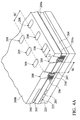
- FIGS. 4A-4C are three-dimensional views showing the steps of forming a chip package according to an embodiment of the present invention.
- FIGS. 5A-5B are plane views showing the steps of forming a chip package according to an embodiment of the present invention.
- FIGS. 6A-6B are plane views showing the steps of forming a chip package according to an embodiment of the present invention.
- FIGS. 7A-7F are cross-sectional views showing the steps of forming a chip package according to an embodiment of the present invention.
- FIGS. 8A-8C are three-dimensional views showing the steps of forming a chip package according to an embodiment of the present invention.
- FIGS. 9A-9B are plane views showing the steps of forming a chip package according to an embodiment of the present invention.
- FIGS. 10A-10B are plane views showing the steps of forming a chip package according to an embodiment of the present invention.
- FIGS. 11A-11F are cross-sectional views showing the steps of forming a chip package according to an embodiment of the present invention.
- FIGS. 12A-12C are three-dimensional views showing the steps of forming a chip package according to an embodiment of the present invention.
- FIGS. 13A-13B are plane views showing the steps of forming a chip package according to an embodiment of the present invention.
- FIGS. 14A-14G are cross-sectional views showing the steps of forming a chip package according to an embodiment of the present invention.
- FIGS. 15A-15C are three-dimensional views showing the steps of forming a chip package according to an embodiment of the present invention.
- FIGS. 16A-16F are cross-sectional views showing the steps of forming a chip package according to an embodiment of the present invention.
- FIGS. 17A-17C are three-dimensional views showing the steps of forming a chip package according to an embodiment of the present invention.
- FIGS. 18A-18B are plane views showing the steps of forming a chip package according to an embodiment of the present invention.
- FIGS. 19A-19F are cross-sectional views showing the steps of forming a chip package according to an embodiment of the present invention.
- FIGS. 20A-20C are three-dimensional views showing the steps of forming a chip package according to an embodiment of the present invention.
- first layer “on,” “overlying,” (and like descriptions) a second layer include embodiments where the first and second layers are in direct contact and those where one or more layers are interposing the first and second layers.
- a chip package according to an embodiment of the present invention may be used to package a MOSFET chip such as a power module chip.
- a MOSFET chip such as a power module chip.
- embodiments of the invention are not limited thereto.
- the chip package of the embodiments of the invention may be applied to package active or passive devices, or electronic components with digital or analog circuits, such as opto electronic devices, micro electro mechanical systems (MEMS), micro fluidic systems, and physical sensors for detecting heat, light, or pressure.
- MEMS micro electro mechanical systems
- a wafer scale package (WSP) process may be applied to package semiconductor chips, such as image sensor devices, light-emitting diodes (LEDs), solar cells, RF circuits, accelerators, gyroscopes, micro actuators, surface acoustic wave devices, pressure sensors, ink printer heads, or power ICs.
- package semiconductor chips such as image sensor devices, light-emitting diodes (LEDs), solar cells, RF circuits, accelerators, gyroscopes, micro actuators, surface acoustic wave devices, pressure sensors, ink printer heads, or power ICs.
- the wafer scale package process mentioned above mainly means that after the package process is accomplished during the wafer stage, the wafer with chips is cut to obtain separate independent packages.
- separate independent chips may be redistributed overlying a supporting wafer and then be packaged, which may also be referred to as a wafer scale package process.
- the above mentioned wafer scale package process may also be adapted to form chip packages of multi-layer integrated circuit devices by stacking a plurality of wafers having integrated circuits.
- the diced package is a chip scale package (CSP).
- the size of the chip scale package (CSP) may only be slightly larger than the size of the packaged chip. For example, the size of the chip package is not larger than 120% of the size of the packaged chip.
- FIG. 1A is a cross-sectional view showing a chip package known by the inventor of the application
- FIG. 1B is a plane view showing a chip 10 known by the inventor of the application, which are used to illustrate problems discovered by the inventor.
- FIG. 1A is a cross-sectional view taken along the line I-I′ of FIG. 1B .
- the packaged chip 10 includes a substrate 100 .
- a device region 102 is formed in the substrate 100 .
- a plurality of conducting pads 106 are disposed on a surface 100 a of the substrate 100 , which are electrically connected to elements in the device region 102 , respectively.
- the conducting pads 106 may be disposed on a periphery region of the substrate 100 .
- the conducting pads 106 may be formed in a dielectric layer 104 formed on the surface 100 a of the substrate 100 .
- a plurality of holes 108 extending from a surface 100 b towards the surface 100 a of the substrate 100 may be formed in the substrate 100 .
- the holes 108 may expose the corresponding conducting pads 106 thereunder, respectively.
- an insulating layer 110 may be formed on the surface 100 b of the substrate 100 , which may extend onto a sidewall of the hole 108 .
- a plurality of wire layers 112 may be formed on the insulating layer 110 and extend into the holes 108 to electrically contact with the conducting pads 106 , respectively and correspondingly.
- the wire layers 112 may further be electrically connected to conducting bumps 116 penetrating a protection layer 114 .
- FIGS. 2A-2F are cross-sectional views showing the steps of forming a chip package according to an embodiment of the present invention.
- FIG. 3A is a plane view corresponding to the structure in FIG. 2B (observed from the surface 200 b ).
- FIG. 3B is a plane view corresponding to the structure shown in FIG. 2F
- FIG. 3C is a plane view corresponding to the structure in FIG. 2B (observed from the surface 200 a ).
- FIGS. 4A-4C are three-dimensional views showing the steps of forming a chip package according to an embodiment of the present invention, which may correspond to the embodiment shown in FIGS. 2A-2F .
- same or similar reference numbers are used to designate same or similar elements.
- the process steps of a chip package includes a front-end chip (wafer) process step and a back-end package process step.
- a front-end chip (wafer) process step Through front-end semiconductor processes such as deposition, etching, and development, a variety of integrated circuits may be formed on a wafer.
- a back-end wafer-level packaging process may be performed to the wafer having integrated circuits formed thereon, followed by a dicing process step to form a plurality of separate chip scale packages.
- a substrate 200 is first provided, which has a surface 200 a and a surface 200 b .
- the substrate 200 is, for example, a semiconductor substrate.
- the substrate 200 is a semiconductor wafer (such as a silicon wafer).
- the substrate 200 may be defined into a plurality of die regions by a plurality of predetermined scribe lines SC.
- a plurality of device regions 202 may be formed or disposed in the substrate 200 .
- each of the die regions of the substrate 200 defined by the predetermined scribe lines SC has at least one device region 202 , and there are a plurality of periphery regions respectively and correspondingly surround the device regions 202 .
- the device region 202 may include active or passive devices, or electronic components with digital or analog circuits, such as opto electronic devices, micro electro mechanical systems (MEMS), micro fluidic systems, and physical sensors for detecting heat, light, or pressure, or power MOSFET modules.
- the device region 202 may include an optoelectronic device such as an image sensor device or a light emitting device.
- At least a dielectric layer may be formed on the surface of the substrate for the use of insulating and covering, which may includes, for example, a dielectric layer 204 a and a dielectric layer 204 .
- a plurality of conducting pads 206 may be formed between the dielectric layer 204 and the substrate 200 .
- the conducting pads 206 may be disposed on, for example, periphery regions of the substrate 200 and be arranged along positions near the predetermined scribe lines SC.
- the conducting pad 206 may be electrically connected to elements in the device region 202 through an interconnection structure (not shown).
- each of the conducting pads 206 may include a stacked structure of a plurality of conducting layers formed in the dielectric layer 204 .
- the stacked conducting layers may be electrically connected to each other through, for example, a metal interconnection structure (not shown).
- the conducting pad 206 is an original conducting pad formed in the dielectric layer 204 in the front-end chip process step and is separated from an edge of the scribe line SC by a predetermined distance. That is, in this embodiment, no extension conducting pad extending to the edge of the scribe line SC or on the scribe line SC needs to be additionally formed. Because all of the conducting pads 206 do not extend into the predetermined scribe lines SC, contact with test structures disposed on the predetermined scribe lines SC may be prevented.
- a plurality of continuous seal ring structures 207 or a plurality of discontinuous seal ring structures 207 may be formed in the dielectric layer 204 , which may be respectively disposed on the periphery regions of the die regions of the substrate 200 (or outside regions of the periphery regions) and surround a portion of the periphery region and the device region 202 therein.
- the seal ring structures 207 and the conducting pads 206 may be simultaneously defined and formed.
- the seal ring structures 207 and the conducting pads 206 may be substantially the same conducting structures.
- the seal ring structure 207 may be disposed on a region outside of the conducting pad 206 or on a region surrounded by two adjacent conducting pads 206 and the edge of the scribe line SC.
- the seal ring structure 207 may protect surrounded devices or circuits structures of the die from being damaged due to stress generated by the dicing process.
- auxiliary optical elements may first be disposed.
- microlenses 205 may be disposed on the device regions 202 , respectively.
- the microlens 205 may include a microlens array.
- the microlens 205 may be used to help light to enter the device region 202 or lead out light emitted from the device region 202 .
- a color filter plate (not shown) may be optionally disposed on the microlens 205 .
- the color filter plate may be disposed, for example, between the microlens 205 and the device region 202 .
- a cover layer 220 may be optionally disposed on the surface 200 a of the substrate 200 .
- the cover layer 220 may be a substrate such as a glass substrate, quartz substrate, transparent polymer substrate, or combinations thereof.
- a spacer layer 218 may be disposed between the cover layer 220 and the substrate 200 .
- the spacer layer 218 may be optionally disposed to partially or completely cover the conducting pad 206 and may further extend across over the predetermined scribe line SC.
- the material of the spacer layer 218 may be, for example, a photosensitive polymer material and may be defined and formed through an exposure process and a development process.
- the spacer layer 218 , the cover layer 220 and the substrate 200 may define a substantially closed cavity 222 on the device region 202 .
- the cavity 222 may contain the microlens 205 .
- the spacer layer 218 may be first formed on the cover layer 220 , followed by being bonded onto the dielectric layer 204 on the substrate 200 . In one embodiment, the spacer layer 218 still has stickiness and may be directly bonded on the substrate 200 . In one embodiment, after the spacer layer 218 is bonded to the substrate 200 , a curing process may be performed to the spacer layer 218 . For example, the spacer layer 218 may be heated. Alternatively, the spacer layer 218 may be bonded onto the substrate 200 through an adhesive (not shown). In another embodiment, the spacer layer 218 may also be first formed on the substrate 200 , and the spacer layer 218 and the cover layer 220 are then bonded.
- the substrate 200 may be optionally thinned.
- the cover layer 220 may be used as a support substrate, and a thinning process (such as a mechanical grinding process or a chemical mechanical polishing process) may be performed to the surface 200 b of the substrate 200 to thin down the substrate 200 to an appropriate thickness.
- a portion of the substrate 200 may be removed from the surface 200 b of the substrate 200 to form a plurality of openings 208 extending towards the surface 200 a .
- a portion of the dielectric layer 204 a may be further removed to expose the conducting pads 206 .
- the openings 208 may expose the corresponding conducting pads 206 and the seal ring structures 207 , respectively.
- a sidewall of the opening 208 may incline to the surface 200 a of the substrate 200 or be substantially perpendicular to the surface 200 a of the substrate 200 .
- a width of the opening 208 gradually increases along a direction extending from a lower opening end 208 b of the opening 208 near the surface 200 b towards an upper opening end 208 a of the opening 208 near the conducting pad 206 or the surface 200 a.
- FIGS. 3A and 4A are a plane view and a three-dimensional view showing the structure corresponding to that shown in FIG. 2B , respectively.
- at least a portion or all of the opening 208 such as a long portion having a length L 1 of the lower opening end 208 b laterally extends into the predetermined scribe line SC.
- the length L 1 of the long portion of the lower opening end 208 b may be set to be larger than a length L 2 of the conducting pad 206 .
- the width of the lower opening end 208 b of the opening 208 may be enlarged to effectively reduce the aspect ratio of the opening 208 such that a material layer subsequently formed in the opening 208 may be smoothly deposited.
- at least a portion or all of the opening 208 such as a wide portion of the upper opening end 208 a is located within an area occupied by the conducting pad 206 .
- At least the width W 1 of the wide portion of the upper opening end 208 a is set to be less or equal to a width W 2 of the conducting pad 206 .
- another substrate region such as a region between two adjacent conducting pads 206 may be disposed with some functional circuit structures to increase available area for forming circuit of the substrate.
- a projection of at least a portion or all of the opening 208 such as the wide portion of the upper opening end 208 a on the upper surface 200 a of the substrate 200 is within a projection area of the conducting pad 206 on the upper surface 200 a of the substrate 200 .
- an insulating layer 210 may be formed on the surface 200 b of the substrate 200 , which may extend into the openings 208 .
- the insulating layer 210 may include, for example, an oxide, nitride, oxynitride, polymer material, or combinations thereof.
- the insulating layer 210 may be formed by using a chemical vapor deposition process, physical vapor deposition process, thermal oxidation process, or coating process. Then, by using a photolithography process and an etching process, a portion of the insulating layer 210 located at the upper opening end 208 a of the opening 208 may be removed to expose the conducting pad 206 .
- a photoresist material is adopted to form the insulating layer 210 .
- an exposure process and a development process may be performed to the insulating layer 210 to pattern the insulating layer 210 such that the conducting pads 206 are exposed.
- a plurality of wire layers 212 are then formed on the insulating layer 210 on the surface 200 b of the substrate 200 .
- Each of the wire layers 212 may extend from the surface 200 b of the substrate 200 into the corresponding opening 208 to electrically contact with the corresponding conducting pad 206 .
- the material of the wire layer 212 may be a conducting material such as a metal material or another suitable conducting material.
- the material of the wire layer 212 may be, for example, copper, aluminum, gold, platinum, or combinations thereof.
- the fabrication method for the wire layer 212 may include a physical vapor deposition process, chemical vapor deposition process, coating process, electroplating process, electroless plating process, or combinations thereof.
- a conducting layer may be first formed on the insulating layer 210 on the surface 200 b of the substrate 200 . Then, through a photolithography process and an etching process, the conducting layer is patterned to be the plurality of wire layers 212 .
- a seed layer (not shown) may be first formed on the insulating layer 210 on the surface 200 b of the substrate 200 . Then, a patterned mask layer (not shown) may be formed on the seed layer. The patterned mask layer may have a plurality of openings exposing a portion of the seed layer. Then, through an electroplating process, a conducting material may be electroplated onto the seed layer exposed by the openings of the patterned mask layer. Then, the patterned mask layer may be removed, and the seed layer originally covered by the patterned mask layer may be removed by using an etching process such that the formation of the wire layers 212 is accomplished.
- FIG. 4B is a three-dimensional view showing the structure corresponding to the structure shown in FIG. 2D .
- the plurality of wire layers 212 extend from positions on the insulating layer 210 on the surface 200 b of the substrate 200 into the openings 208 , respectively and correspondingly, to electrically contact with the corresponding conducting pads 206 below the corresponding openings 208 .
- each of the wire layers 212 does not extend into the predetermined scribe lines SC or is separated from the predetermined scribe line SC by a distance.
- a cutting blade is not in contact with the wire layers 212 to cause damage or peeling of the wire layers 212 .
- the wire layers 212 are separated from the seal ring structures 217 by the insulating layer 210 such that no short circuiting forms between the wire layers 212 .
- a protection layer 214 is formed on the surface 200 b of the substrate 200 .
- the protection layer 214 may cover the substrate 200 , the wire layers 212 , and the openings 208 .
- the protection layer 214 may include a solder mask material, green paint, polyimide, or another suitable insulating material.
- the protection layer 214 may be formed by using, for example, a coating process or a spray coating process. Then, the protection layer 214 may be patterned to have openings exposing a portion of the wire layers 212 .
- the protection layer 214 includes a positive type photoresist layer.
- the protection layer 214 is set to be not extended into the predetermined scribe lines SC.
- a cutting blade does not cut the protection layer 214 such that the protection layer 214 is prevented from being damaged, and high stress of the protection layer 214 is prevented from affecting other material layers.
- conducting bumps 216 may be formed on the exposed wire layers 212 , which may be, for example, solder balls.
- under bump metallurgy layers (not shown) may be first formed on the exposed wire layers 212 to facilitate the formation of the conducting bumps 216 .
- FIG. 2F is a cross-sectional view showing one of the chip packages
- FIGS. 3B and 4C respectively show a plane view and a three-dimensional view of the structure corresponding to the structure shown in FIG. 2F .
- an edge of the protection layer 214 of the chip package is not coplanar with edges of the chip and/or the dielectric layer 204 , and the edges are separated from each other by a distance d.
- a portion of the opening 208 becomes an opening 208 c located at a side surface 200 c of the substrate of the chip package, as shown in FIG. 3B or FIG. 4C .
- the opening 208 c may further have a lateral portion located on an edge of the chip.
- the openings 208 c may be set to extend along a direction intersecting the edge of the chip (such as the side surface 200 c of the substrate 200 which connect the surfaces 200 a and 200 b ) to extend beyond the region occupied by the conducing pads.
- the opening 208 c may extend towards the edge of the chip.
- the two openings 208 c may also be separated from each other by the substrate 200 therebetween. In other words, the two adjacent openings 208 c do not connect with each other and are separated from each other by the substrate 200 .
- the extending portion (wide portion) of the openings 208 c extending along a direction substantially parallel to the edge of the chip (such as the side surface 200 c ) are still located within the occupation regions of the conducting pads without extending beyond the conducting pads. That is, the width W 1 of the wide portion of the opening 208 c may be smaller than or equal to the width W 2 of the conducting pad 206 .
- the conducting pad 206 is separated from the edge of the side surface 200 c of the substrate 200 by a distance.
- a plurality of openings 208 c may be arranged a same side surface or different side surfaces of the substrate 200 .
- the wire layer 212 in the opening 208 c does not extend to the edge of the chip or is not coplanar with the side surface 200 c of the substrate 200 and a distance is therebetween.
- a long axis direction of the opening 208 c may be substantially perpendicular to or incline to the side surface 200 c of the substrate 200 , wherein the long axis direction may be substantially parallel to a connection line between two farthest terminal points of the opening 208 c .
- a portion (long portion) of the opening 208 c extending along the long axis direction may intersect the side surface 200 c of the substrate 200 , and the long axis direction of the opening 208 c may be substantially parallel to a normal vector of the intersected side surface 200 c .
- a contact interface between the wire layer 212 and the corresponding conducting pad 206 is separated from the side surface 200 c of the substrate 200 by a distance.
- the conducting pad 206 is located within an edge surface of the chip, wherein the edge of the chip may be formed by the substrate 200 and the dielectric layers 204 and 204 a.
- FIGS. 5A-5B are plane views showing the steps of forming a chip package according to another embodiment of the present invention, wherein same or similar reference numbers are used to designate same or similar elements.
- the conducting pads 206 in adjacent die regions along both sides of the predetermined scribe line SC are asymmetrically disposed.
- the openings 208 along both sides of the predetermined scribe line SC are also asymmetrically disposed.
- the sidewall of the opening 208 may incline to the predetermined scribe line SC.
- FIG. 5B is a plane view showing the chip package obtained from performing process steps similar to those illustrated in FIGS. 2-4 to the structure shown in FIG. 5A .
- a plurality of conducting pads 206 are disposed on a first periphery region of the substrate 200 (such as the periphery region of the substrate 200 on the left side), and the other plurality of conducting pads 206 are disposed on a second periphery region of the substrate 200 (such as the periphery region of the substrate 200 on the right side).
- the conducting pads 206 disposed on the first periphery region are not asymmetrical to the conducting pads 206 disposed on the second periphery region.
- the openings 208 c exposing the conducting pads 206 on the first periphery region are also not symmetrical to the openings 208 c exposing the conducting pads 206 on the second periphery region.
- a sidewall of the opening 208 c intersects the side surface 200 c of the substrate 200 , and the angle therebetween is less than 90 degree.
- a sidewall of the opening 208 c intersects the side surface 200 c of the substrate 200 , and the angle therebetween is substantially equal to 90 degree.
- FIGS. 6A-6B are plane views showing the steps of forming a chip package according to an embodiment of the present invention.
- FIGS. 7A-7F are cross-sectional views showing the steps of forming a chip package corresponding to the embodiment shown in FIG. 6 .
- FIGS. 8A-8C are three-dimensional views showing the steps of forming a chip package corresponding to the embodiment shown in FIG. 6 .
- same or similar reference numbers are used to designate same or similar elements.
- FIG. 7A in one embodiment, a structure similar to that shown in FIG. 2A is provided.
- FIG. 7B through, for example, a photolithography process and an etching process, a portion of the substrate 200 is removed to form a plurality of openings 208 extending from the surface 200 b towards the surface 200 a of the substrate 200 .
- a portion of the dielectric layer 204 a may be further removed to expose the conducting pads 206 .
- the openings 208 may expose the conducting pads 206 and the seal ring structures 207 , respectively and correspondingly.
- FIGS. 6A and 8A are a plane view and a three-dimensional view showing the structure corresponding to that shown in FIG. 7B , respectively.
- the openings 208 respectively extend from the corresponding conducting pads 206 into the corresponding predetermined scribe lines SC and further extend towards the conducting pads along another side of the predetermined scribe line SC to expose the conducting pads on the other side. That is, the opening 208 may extend across over the predetermined scribe line SC to expose the conducting pads in two adjacent die regions.
- a width of the opening 208 is smaller than or equal to a width of the conducting pad 206 .
- the opening 208 extends from the conducting pad 206 into the predetermined scribe line SC and extends to the conducting pad 206 on the other side, the aspect ratio of the opening 208 is thus reduced, which facilitates subsequent depositions of a variety of material layers in the opening 208 .
- an insulating layer 210 may be formed on the surface 200 b of the substrate 200 , which may extend into the openings 208 . Then, by using a photolithography process and an etching process, a portion of the insulating layer 210 located on the bottom of the opening 208 may be removed to expose the conducting pad 206 . In one embodiment, it is preferable that the insulating layer 210 still completely covers the seal ring structures 207 to prevent subsequently formed wire layers from contacting with the seal ring structures 207 and causing a short circuiting.
- a plurality of wire layers 212 are then formed on the insulating layer 210 on the surface 200 b of the substrate 200 .
- Each of the wire layers 212 may extend from the surface 200 b of the substrate 200 into the corresponding opening 208 to electrically contact with the corresponding conducting pad 206 .
- FIG. 8B is a three-dimensional view showing the structure corresponding to the structure shown in FIG. 7D .
- the plurality of wire layers 212 extend from positions on the insulating layer 210 on the surface 200 b of the substrate 200 into the openings 208 , respectively and correspondingly, to electrically contact with the corresponding conducting pads 206 below the corresponding openings 208 .
- each of the wire layers 212 does not extend into the predetermined scribe lines SC or is separated from the predetermined scribe line SC by a distance.
- the wire layers 212 are separated from the seal ring structures 217 by the insulating layer 210 such that no short circuiting forms between the wire layers 212 .
- the opening 208 extends across over the predetermined scribe line SC and has a wider width, it is easier to form an insulating layer or a conducting layer in the opening 208 .
- a protection layer 214 is formed on the surface 200 b of the substrate 200 .
- the protection layer 214 may cover the substrate 200 , the wire layers 212 , and the openings 208 .
- the protection layer 214 may be patterned to have openings exposing a portion of the wire layers 212 .
- the protection layer 214 is set to be not extended into the predetermined scribe lines SC.
- conducting bumps 216 may be formed on the exposed wire layers 212 , which may be, for example, solder balls.
- FIG. 7F is a cross-sectional view showing one of the chip packages
- FIGS. 6B and 8C respectively show a plane view and a three-dimensional view of the structure corresponding to the structure shown in FIG. 7F .
- an edge of the protection layer 214 of the chip package is not coplanar with edges of the chip and/or the dielectric layer 204 , and the edges are separated from each other by a distance d.
- a portion of the opening 208 becomes an opening 208 c located at a side surface 200 c of the substrate of the chip package, as shown in FIG. 6B or FIG. 8C .
- the chip package of the embodiment may be substantially similar to the chip package of the embodiment shown in FIGS. 2F , 3 B, and 4 C.
- the openings 208 c exposes the corresponding conducting pad 206 and extends towards the side surface 200 c of the substrate 200 along a direction intersecting the side surface 200 c of the substrate 200 to extend beyond the conducing pads 206 .
- the opening 208 c extends to the side surface 200 c of the substrate 200 , as shown in FIG. 8C .
- FIGS. 9A-9B are plane views showing the steps of forming a chip package according to an embodiment of the present invention, wherein same or similar reference numbers are used to designate same or similar elements.
- the conducting pads 206 in the adjacent die regions along both sides of the predetermined scribe lines SC are asymmetrically disposed.
- the openings 208 may have many variations.
- the opening 208 may extend across over the predetermined scribe line SC to expose the conducting pads 206 in two adjacent die regions, and a sidewall of the opening 208 may incline to the conducting pad 206 .
- the opening 208 may have a variety of shapes such as (but is not limited to) a sector, rectangle, or ellipse.
- the opening 208 may have a turning portion.
- the opening 208 may extend over the conducting pad 206 . Any arrangement, shape, combination, or inclining way of the sidewall of the opening of the opening, which can help a subsequent deposition of material layers, is within the scope of the embodiments of the invention.
- FIG. 9B is a plane view showing the chip package obtained from performing process steps similar to those illustrated in FIGS. 2-4 to the structure shown in FIG. 9A .
- a plurality of conducting pads 206 are disposed on a first periphery region of the substrate 200 (such as the periphery region of the substrate 200 on the left side), and the other plurality of conducting pads 206 are disposed on a second periphery region of the substrate 200 (such as the periphery region of the substrate 200 on the right side).
- the conducting pads 206 disposed on the first periphery region are not asymmetrical to the conducting pads 206 disposed on the second periphery region.
- the openings 208 c exposing the conducting pads 206 on the first periphery region are also not symmetrical to the openings 208 c exposing the conducting pads 206 on the second periphery region.
- angles between the sidewalls of the different openings 208 c and the side surface of the substrate 200 are not completely the same. Angles between the sidewalls of the different openings 208 and the edges of the conducting pads 206 are also not completely the same.
- FIGS. 10A-10B are plane views showing the steps of forming a chip package according to an embodiment of the present invention.
- FIGS. 11A-11F are cross-sectional views showing the steps of forming a chip package corresponding to the embodiment shown in FIG. 10 .
- FIGS. 12A-12C are three-dimensional views showing the steps of forming a chip package corresponding to the embodiment shown in FIG. 10 .
- same or similar reference numbers are used to designate same or similar elements.
- FIG. 11A in one embodiment, a structure similar to that shown in FIG. 2A is provided.
- FIG. 11B through, for example, a photolithography process and an etching process, a portion of the substrate 200 is removed to form a plurality of openings 208 extending from the surface 200 b towards the surface 200 a of the substrate 200 .
- a portion of the dielectric layer 204 a may be further removed to expose the conducting pads 206 .
- the openings 208 may expose the conducting pads 206 and the seal ring structures 207 , respectively and correspondingly.
- a portion of the substrate 200 may be optionally removed to form a plurality of recesses 208 ′ (which is, for example, trenches) extending from the surface 200 b towards the surface 200 a of the substrate 200 .
- the recesses 208 ′ may connect with the openings 208 mentioned above.
- the openings 208 and the recesses 208 ′ may be formed in a same patterning process.
- FIGS. 10A and 12A are a plane view and a three-dimensional view showing the structure corresponding to that shown in FIG. 11B , respectively.
- the openings 208 respectively extend from the corresponding conducting pads 206 into the corresponding predetermined scribe lines SC to connect with the formed recesses 208 ′ and further extend towards the conducting pads along another side of the predetermined scribe line SC to expose the conducting pads on the other side. That is, the opening 208 may extend across over the predetermined scribe line SC to connect with the recess 208 ′ and extend to the conducting pad 206 in another die region to expose the conducting pads 206 in two adjacent die regions.
- a width of the opening 208 is smaller than or equal to a width of the conducting pad 206 . Because the opening 208 extends from the conducting pad 206 into the predetermined scribe line SC to connect with the recess 208 ′ and extends to the conducting pad 206 on the other side, the aspect ratio of the opening (including the opening 208 and the recess 208 ′) is thus reduced, which facilitates subsequent depositions of a variety of material layers in the opening.
- an insulating layer 210 may be formed on the surface 200 b of the substrate 200 , which may extend into the openings 208 . Then, by using a photolithography process and an etching process, a portion of the insulating layer 210 located on the bottom of the opening 208 may be removed to expose the conducting pad 206 . In one embodiment, it is preferable that the insulating layer 210 still completely covers the seal ring structures 207 to prevent subsequently formed wire layers from contacting with the seal ring structures 207 and causing a short circuiting.
- a plurality of wire layers 212 are then formed on the insulating layer 210 on the surface 200 b of the substrate 200 .
- Each of the wire layers 212 may extend from the surface 200 b of the substrate 200 into the corresponding opening 208 to electrically contact with the corresponding conducting pad 206 .
- FIG. 12B is a three-dimensional view showing the structure corresponding to the structure shown in FIG. 11D .
- the plurality of wire layers 212 extend from positions on the insulating layer 210 on the surface 200 b of the substrate 200 into the openings 208 , respectively and correspondingly, to electrically contact with the corresponding conducting pads 206 below the corresponding openings 208 .
- each of the wire layers 212 does not extend into the predetermined scribe lines SC or is separated from the predetermined scribe line SC by a distance.
- the wire layers 212 are separated from the seal ring structures 217 by the insulating layer 210 such that no short circuiting forms between the wire layers 212 .
- the opening 208 extends across over the predetermined scribe line SC and connects with the recess 208 ′ to have a wider width, it is easier to form an insulating layer or a conducting layer in the opening 208 .
- a protection layer 214 is formed on the surface 200 b of the substrate 200 .
- the protection layer 214 may cover the substrate 200 , the wire layers 212 , the openings 208 , and the recesses 208 ′.
- the protection layer 214 may be patterned to have openings exposing a portion of the wire layers 212 .
- the protection layer 214 is set to be not extended into the predetermined scribe lines SC (not shown).
- conducting bumps 216 may be formed on the exposed wire layers 212 , which may be, for example, solder balls.
- FIG. 11F is a cross-sectional view showing one of the chip packages
- FIGS. 10B and 12C respectively show a plane view and a three-dimensional view of the structure corresponding to the structure shown in FIG. 11F .
- a portion of the opening 208 becomes an opening 208 c located at a side surface 200 c of the substrate of the chip package, as shown in FIG. 10B or FIG. 12C .
- the chip package of the embodiment may be substantially similar to the chip package of the embodiment shown in FIGS. 2F , 3 B, and 4 C.
- the openings 208 c exposes the corresponding conducting pad 206 and extends towards the side surface 200 c of the substrate 200 along a direction intersecting the side surface 200 c of the substrate 200 to extend beyond the conducing pads 206 .
- the opening 208 c extends to the side surface 200 c of the substrate 200 , as shown in FIG. 12C .
- FIGS. 13A-13B are plane views showing the steps of forming a chip package according to an embodiment of the present invention.
- FIGS. 14A-14G are cross-sectional views showing the steps of forming a chip package corresponding to the embodiment shown in FIG. 13 .
- FIGS. 15A-15C are three-dimensional views showing the steps of forming a chip package corresponding to the embodiment shown in FIG. 13 .
- same or similar reference numbers are used to designate same or similar elements.
- FIG. 14A in one embodiment, a structure similar to that shown in FIG. 2A is provided.
- FIG. 14B through, for example, a photolithography process and an etching process, a portion of the substrate 200 is removed to form a plurality of openings 208 extending from the surface 200 b towards the surface 200 a of the substrate 200 .
- a width of the opening 208 gradually increases along a direction extending from the surface 200 b of the substrate 200 towards the conducting pad 206 .
- the openings 208 as shown in FIG. 14B may be formed.
- a portion of the dielectric layer 204 a may be further removed to expose the conducting pads 206 .
- the seal ring structure 207 disposed in the dielectric layer 204 includes a plurality of seal rings which are disposed along edges of the predetermined scribe lines SC, respectively, and do not overlap the openings 208 . That is, the openings 208 do not expose the seal ring structures 207 .
- the seal ring structure 207 is located outside of the projection region of the opening 208 on the dielectric layer 204 . In one embodiment, the seal ring structure is discontinuous.
- a portion of the substrate 200 may be optionally removed to form a plurality of recesses 208 ′ (which is, for example, trenches) extending from the surface 200 b towards the surface 200 a of the substrate 200 .
- the recesses 208 ′ may connect with the openings 208 mentioned above.
- the openings 208 and the recesses 208 ′ may be formed in a same patterning process.
- a width of the recess 208 ′ gradually increases along a direction extending from the surface 200 b of the substrate 200 towards the conducting pad 206 .
- FIGS. 13A and 15A are a plane view and a three-dimensional view showing the structure corresponding to that shown in FIG. 14B , respectively.
- the openings 208 respectively extend from the corresponding conducting pads 206 into the corresponding predetermined scribe lines SC to connect with the formed recesses 208 ′ and further extend towards the conducting pads along another side of the predetermined scribe line SC to expose the conducting pads on the other side. That is, the opening 208 may extend across over the predetermined scribe line SC to connect with the recess 208 ′ and extend to the conducting pad 206 in another die region to expose the conducting pads 206 in two adjacent die regions.
- a width of the opening 208 is smaller than or equal to a width of the conducting pad 206 . Because the opening 208 extends from the conducting pad 206 into the predetermined scribe line SC to connect with the recess 208 ′ and extends to the conducting pad 206 on the other side, the aspect ratio of the opening 208 is thus reduced, which facilitates subsequent depositions of a variety of material layers in the opening 208 .
- an insulating layer 210 may be formed on the surface 200 b of the substrate 200 , which may extend into the openings 208 .
- the width of the opening 208 gradually increases along a direction extending from the surface 200 b towards the conducting pad 206
- a thickness of the formed insulating layer 210 on the sidewall of the opening 208 may gradually decrease along a direction extending from the surface 200 b towards the conducting pad 206 . It is possible that because the portion of the opening 208 near the surface 200 b has a smaller width, the insulating material used for forming the insulating layer 210 is blocked by the substrate 200 and can not easily enter the opening 208 . Thus, the thickness of the insulating layer 210 on the sidewall of the opening 208 gradually decreases along a direction towards an inner portion of the opening.
- a portion of the insulating layer 210 located on the bottom of the opening 208 may be removed to form a patterned insulating layer 210 ′ such that the conducting pads 206 are exposed.
- the insulating layer on the surface 200 b of the substrate 200 may be directly used as a mask, and an etching process is performed to the insulating layer 210 on the bottom of the opening 208 to form the patterned insulating layer 210 ′, wherein the etching process is, for example, (but is not limited to) a dry etching process.
- the thinner insulating layer 210 on the bottom of the opening 208 when the thinner insulating layer 210 on the bottom of the opening 208 is etched and removed, the insulating layer 210 on the sidewall of the opening 208 only becomes thinner and still partially remains on the sidewall of the opening 208 to be a portion of the patterned insulating layer 210 ′.
- the thickness of the insulating layer 210 on the surface 200 b is thicker, the insulating layer on the surface 200 b of the substrate 200 only becomes thinner and still remains on the surface 200 b of the substrate 200 to be a portion of the patterned insulating layer 210 ′ when the insulating layer 210 on the bottom of the opening 208 is removed.
- a thickness of a portion of the patterned insulating layer 210 ′ extending on the sidewall of the opening 208 gradually decreases along a direction extending from the surface 200 b towards the conducting pad 206 .
- the insulating layer on the bottom of the opening 208 is substantially removed.
- the seal ring structure 207 as shown in FIG. 13A may be adopted.
- the opening 208 may expose the seal ring structure. In this case, the wire layers may be prevented from contacting with the exposed seal ring structure through the control of the patterning process of the wire layers.
- a plurality of wire layers 212 are formed on the insulating layer 210 on the surface 200 b of the substrate 200 .
- Each of the wire layers 212 may extend from the surface 200 b of the substrate 200 into the corresponding opening 208 to electrically contact with the corresponding conducting pad 206 .
- FIG. 15B is a three-dimensional view showing the structure corresponding to the structure shown in FIG. 14E .
- the plurality of wire layers 212 extend from positions on the insulating layer 210 ′ on the surface 200 b of the substrate 200 into the openings 208 , respectively and correspondingly, to electrically contact with the corresponding conducting pads 206 below the corresponding openings 208 .
- each of the wire layers 212 does not extend into the predetermined scribe lines SC or is separated from the predetermined scribe line SC by a distance. Thus, when a dicing process is subsequently performed along the predetermined scribe lines SC, a cutting blade is not in contact with the wire layers 212 to cause damage or peeling of the wire layers 212 .
- the opening 208 does not expose the seal ring structure 207 .
- the wire layers 212 formed in the openings 208 are not in contact with the seal ring structures 207 . Thus, no short circuiting is formed between the wire layers 212 .
- the opening 208 extends across over the predetermined scribe line SC and connects with the recess 208 ′ to have a wider width, it is easier to form an insulating layer or a conducting layer in the opening 208 .
- the patterned insulating layer 210 ′ may be formed directly by using an etching process, processes such as an exposure process, development process, removing process of a patterned mask layer may not be needed. Fabrication time and cost may be reduced.
- a protection layer 214 is formed on the surface 200 b of the substrate 200 .
- the protection layer 214 may cover the substrate 200 , the wire layers 212 , and the openings 208 .
- the protection layer 214 may be patterned to have openings exposing a portion of the wire layers 212 .
- conducting bumps 216 may be formed on the exposed wire layers 212 , which may be, for example, solder balls.
- FIG. 14G is a cross-sectional view showing one of the chip packages
- FIGS. 13B and 15C respectively show a plane view and a three-dimensional view of the structure corresponding to the structure shown in FIG. 14G .
- a portion of the opening 208 becomes an opening 208 c located at a side surface 200 c of the substrate of the chip package, as shown in FIG. 13B or FIG. 15 C.
- the chip package of the embodiment may be substantially similar to the chip package of the embodiment shown in FIGS. 2F , 3 B, and 4 C, wherein one of the main differences is that the wide of the opening 208 c gradually increases along a direction extending from the surface 200 b towards the conducting pad 206 .
- the openings 208 c exposes the corresponding conducting pad 206 and extends towards the side surface 200 c of the substrate 200 along a direction intersecting the side surface 200 c of the substrate 200 to extend beyond the conducing pads 206 .
- the opening 208 c extends to the side surface 200 c of the substrate 200 , as shown in FIG. 15C .
- FIGS. 16A-16F are cross-sectional views showing the steps of forming a chip package according to an embodiment of the present invention.
- FIGS. 17A-17C are three-dimensional views showing the steps of forming a chip package corresponding to the embodiment shown in FIG. 16 .
- same or similar reference numbers are used to designate same or similar elements.
- a substrate 200 similar to that shown in FIG. 2A is provided.
- device regions 202 may be formed in the substrate 200 .
- the device region 202 may include opto electronic devices, micro electro mechanical systems (MEMS), micro fluidic systems, and physical sensors for detecting heat, light, or pressure, or power MOSFET modules.
- a dielectric layers 204 a and 204 , conducting pads 206 , and seal ring structures 207 may be disposed on the surface 200 a of the substrate 200 .
- a plurality of predetermined scribe lines SC define the substrate 200 into a plurality of die regions. After a subsequent dicing process is performed along the predetermined scribe lines SC, each die region becomes the chip in the formed chip package.
- a carrier substrate 300 may be optionally disposed on the dielectric layer 204 on the surface 200 a of the substrate 200 .
- the carrier substrate 300 is a substrate which can be easily removed in a subsequent process.
- the carrier substrate 300 may include, for example, a silicon substrate, glass substrate, ceramic substrate, polymer substrate, or combinations thereof.
- the carrier substrate 300 may be bonded onto the dielectric layer 204 through an adhesion layer (not shown). In one embodiment, the adhesion layer is capable of being easily removed such that the carrier substrate 300 may also be together removed from the surface 200 a of the substrate 200 .
- the used adhesion layer may lose stickiness when being irradiated with specific light, dipped in specific solution, or kept in specific temperature, such that the carrier substrate 300 may be easily removed.
- the carrier substrate 300 may not be disposed, and subsequent processes are directly performed.
- a UV tape may be attached onto the substrate 200 or the dielectric layer 204 to fix the substrate 200 to facilitate proceeding of the subsequent processes.
- a portion of the substrate 200 is removed to form a plurality of openings 208 extending from the surface 200 b towards the surface 200 a of the substrate 200 .
- a portion of the dielectric layer 204 a may be further removed to expose the conducting pads 206 .
- the openings 208 may expose the conducting pads 206 and the seal ring structures 207 , respectively and correspondingly.
- a portion of the substrate 200 may be optionally removed to form a plurality of recesses 208 ′ (which is, for example, trenches) extending from the surface 200 b towards the surface 200 a of the substrate 200 .
- the recesses 208 ′ may connect with the openings 208 mentioned above.
- the openings 208 and the recesses 208 ′ may be formed in a same patterning process.
- FIG. 17A is a three-dimensional view showing the structure corresponding to that shown in FIG. 16B .
- the openings 208 respectively extend from the corresponding conducting pads 206 into the corresponding predetermined scribe lines SC to connect with the formed recesses 208 ′ and further extend towards the conducting pads along another side of the predetermined scribe line SC to expose the conducting pads on the other side. That is, the opening 208 may extend across over the predetermined scribe line SC to connect with the recess 208 ′ and extend to the conducting pad 206 in another die region to expose the conducting pads 206 in two adjacent die regions.
- an insulating layer 210 may be formed on the surface 200 b of the substrate 200 , which may extend into the openings 208 . Then, by using a photolithography process and an etching process, a portion of the insulating layer 210 located on the bottom of the opening 208 may be removed to expose the conducting pad 206 . In one embodiment, it is preferable that the insulating layer 210 still completely covers the seal ring structures 207 to prevent subsequently formed wire layers from contacting with the seal ring structures 207 and causing a short circuiting.
- a plurality of wire layers 212 are then formed on the insulating layer 210 on the surface 200 b of the substrate 200 .
- Each of the wire layers 212 may extend from the surface 200 b of the substrate 200 into the corresponding opening 208 to electrically contact with the corresponding conducting pad 206 .
- FIG. 17B is a three-dimensional view showing the structure corresponding to the structure shown in FIG. 16D .
- the plurality of wire layers 212 extend from positions on the insulating layer 210 on the surface 200 b of the substrate 200 into the openings 208 , respectively and correspondingly, to electrically contact with the corresponding conducting pads 206 below the corresponding openings 208 .
- each of the wire layers 212 does not extend into the predetermined scribe lines SC or is separated from the predetermined scribe line SC by a distance.
- the wire layers 212 are separated from the seal ring structures 217 by the insulating layer 210 such that no short circuiting forms between the wire layers 212 .
- the opening 208 extends across over the predetermined scribe line SC and connects with the recess 208 ′ to have a wider width, it is easier to form an insulating layer or a conducting layer in the opening 208 .
- a protection layer 214 is formed on the surface 200 b of the substrate 200 .
- the protection layer 214 may cover the substrate 200 , the wire layers 212 , and the openings 208 .
- the protection layer 214 may be patterned to have openings exposing a portion of the wire layers 212 .
- conducting bumps 216 may be formed on the exposed wire layers 212 , which may be, for example, solder balls.
- FIG. 16F is a cross-sectional view showing one of the chip packages
- FIG. 17C shows a three-dimensional view of the structure corresponding to the structure shown in FIG. 16F
- an edge of the protection layer 214 of the chip package may also not be coplanar with edges of the chip and/or the dielectric layer 204 , and a distance d (not shown) is therebetween.
- the chip package of the embodiment may be substantially similar to the chip package of the embodiment shown in FIGS. 2F , 3 B, and 4 C, wherein the main difference is that this embodiment has no spacer layer, cover layer, and microlens.
- the openings 208 c exposes the corresponding conducting pad 206 and extends towards the side surface 200 c of the substrate 200 along a direction intersecting the side surface 200 c of the substrate 200 to extend beyond the conducing pads 206 .
- the opening 208 c extends to the side surface 200 c of the substrate 200 , as shown in FIG. 17C .
- the chip package may have the carrier substrate 300 or may have no carrier substrate 300 .
- the carrier substrate 300 may be removed before the dicing process is performed.
- no carrier substrate has been disposed on the dielectric layer 204 .
- FIGS. 18A-18B are plane views showing the steps of forming a chip package according to an embodiment of the present invention.
- FIGS. 19A-19F are cross-sectional views showing the steps of forming a chip package corresponding to the embodiment shown in FIG. 18 .
- FIGS. 20A-20C are three-dimensional views showing the steps of forming a chip package corresponding to the embodiment shown in FIG. 18 .
- same or similar reference numbers are used to designate same or similar elements.
- FIG. 19A in one embodiment, a structure similar to that shown in FIG. 2A is provided.
- FIG. 19B through, for example, a photolithography process and an etching process, a portion of the substrate 200 is removed to form a plurality of recesses 209 extending from the surface 200 b towards the surface 200 a of the substrate 200 .
- the recesses 209 may be, for example, trenches which may overlap the predetermined scribe lines SC.
- a bottom of the recess 209 is the substantially planar substrate 200 .
- a portion of the substrate 200 may then be removed by using, for example, a photolithography process and an etching process to form a plurality of opening 208 extending from the bottoms of the recesses 209 towards the surface 200 a . Because the opening 208 is formed from a surface of the substrate 200 at the bottom of the recess 209 , the formed opening 208 has a smaller depth contributing to a smaller aspect ratio, which facilitates the proceeding of subsequent processes.
- a portion of the dielectric layer 204 a may be further removed to expose the conducting pads 206 .
- the openings 208 may expose the conducting pads 206 and the seal ring structures 207 , respectively and correspondingly.
- a portion of the substrate 200 may be optionally removed to form a plurality of recesses 208 ′ (which is, for example, trenches) extending from the surface 200 b towards the surface 200 a of the substrate 200 .
- the recesses 208 ′ may connect with the openings 208 mentioned above.
- the openings 208 and the recesses 208 ′ may be formed in a same patterning process.
- FIGS. 18A and 20A are a plane view and a three-dimensional view showing the structure corresponding to that shown in FIG. 19B , respectively.
- the openings 208 respectively extend from the corresponding conducting pads 206 into the corresponding predetermined scribe lines SC to connect with the formed recesses 208 ′ and further extend towards the conducting pads along another side of the predetermined scribe line SC to expose the conducting pads on the other side. That is, the opening 208 may extend across over the predetermined scribe line SC to connect with the recess 208 ′ and extend to the conducting pad 206 in another die region to expose the conducting pads 206 in two adjacent die regions.
- the openings 208 further connect with the recesses 209 such that subsequent deposition of material layers (such as an insulating layer and wire layers) is easier.
- an insulating layer 210 may be formed on the surface 200 b of the substrate 200 , which may extend onto sidewalls of the recesses 209 and the openings 208 . Then, by using a photolithography process and an etching process, a portion of the insulating layer 210 located on the bottom of the opening 208 may be removed to expose the conducting pad 206 . In one embodiment, it is preferable that the insulating layer 210 still completely covers the seal ring structures 207 to prevent subsequently formed wire layers from contacting with the seal ring structures 207 and causing a short circuiting.
- a plurality of wire layers 212 are then formed on the insulating layer 210 on the surface 200 b of the substrate 200 .
- Each of the wire layers 212 may extend from the surface 200 b of the substrate 200 into the corresponding opening 208 to electrically contact with the corresponding conducting pad 206 .
- FIG. 20B is a three-dimensional view showing the structure corresponding to the structure shown in FIG. 19D .
- the plurality of wire layers 212 extend from positions on the insulating layer 210 on the surface 200 b of the substrate 200 into the recesses 209 and further extend into the openings 208 , respectively and correspondingly, to electrically contact with the corresponding conducting pads 206 below the corresponding openings 208 .
- each of the wire layers 212 does not extend into the predetermined scribe lines SC or is separated from the predetermined scribe line SC by a distance.
- the wire layers 212 are separated from the seal ring structures 217 by the insulating layer 210 such that no short circuiting forms between the wire layers 212 .
- the opening 208 connects with the recess 209 and extends across over the predetermined scribe line SC to connect with the recess 208 ′ to have a wider width, it is easier to form an insulating layer or a conducting layer in the opening 208 .
- a protection layer 214 is formed on the surface 200 b of the substrate 200 .
- the protection layer 214 may cover the substrate 200 , the wire layers 212 , and the openings 208 .
- the protection layer 214 may be patterned to have openings exposing a portion of the wire layers 212 .
- conducting bumps 216 may be formed on the exposed wire layers 212 , which may be, for example, solder balls.
- FIG. 19F is a cross-sectional view showing one of the chip packages
- FIGS. 18B and 20C respectively show a plane view and a three-dimensional view of the structure corresponding to the structure shown in FIG. 19F .
- an edge of the protection layer 214 may be set to be not coplanar with edges of the chip and/or the dielectric layer 204 and a distance is therebetween (not shown).
- a portion of the opening 208 becomes an opening 208 c located at a side surface 200 c of the substrate of the chip package, and a portion of the recess 209 become a recess 209 a or 209 b located at an edge of the substrate of the chip package, as shown in FIG. 18B or FIG. 20C .
- the chip package of the embodiment may be substantially similar to the chip package of the embodiment shown in FIGS. 2F , 3 B, and 4 C, wherein the main difference is that the chip package of this embodiment further include the recess 209 a and/or the recess 209 b .
- the openings 208 c exposes the corresponding conducting pad 206 and extends towards the side surface 200 c of the substrate 200 along a direction intersecting the side surface 200 c of the substrate 200 to extend beyond the conducing pads 206 .
- the opening 208 c extends to the side surface 200 c of the substrate 200 , as shown in FIG. 20C .
- the packaging technique of the embodiments of the invention may effectively reduce the process difficulty of forming the wire layer electrically connected to the conducting pad in the chip package.
Landscapes
- Engineering & Computer Science (AREA)
- Physics & Mathematics (AREA)
- Condensed Matter Physics & Semiconductors (AREA)
- General Physics & Mathematics (AREA)
- Computer Hardware Design (AREA)
- Microelectronics & Electronic Packaging (AREA)
- Power Engineering (AREA)
- Manufacturing & Machinery (AREA)
- Internal Circuitry In Semiconductor Integrated Circuit Devices (AREA)
Priority Applications (2)
| Application Number | Priority Date | Filing Date | Title |
|---|---|---|---|
| US13/678,507 US8803326B2 (en) | 2011-11-15 | 2012-11-15 | Chip package |
| US14/337,011 US9018770B2 (en) | 2011-11-15 | 2014-07-21 | Chip package |
Applications Claiming Priority (2)
| Application Number | Priority Date | Filing Date | Title |
|---|---|---|---|
| US201161559868P | 2011-11-15 | 2011-11-15 | |
| US13/678,507 US8803326B2 (en) | 2011-11-15 | 2012-11-15 | Chip package |
Related Child Applications (1)
| Application Number | Title | Priority Date | Filing Date |
|---|---|---|---|
| US14/337,011 Division US9018770B2 (en) | 2011-11-15 | 2014-07-21 | Chip package |
Publications (2)
| Publication Number | Publication Date |
|---|---|
| US20130119556A1 US20130119556A1 (en) | 2013-05-16 |
| US8803326B2 true US8803326B2 (en) | 2014-08-12 |
Family
ID=48279824
Family Applications (2)
| Application Number | Title | Priority Date | Filing Date |
|---|---|---|---|
| US13/678,507 Active US8803326B2 (en) | 2011-11-15 | 2012-11-15 | Chip package |
| US14/337,011 Active US9018770B2 (en) | 2011-11-15 | 2014-07-21 | Chip package |
Family Applications After (1)
| Application Number | Title | Priority Date | Filing Date |
|---|---|---|---|
| US14/337,011 Active US9018770B2 (en) | 2011-11-15 | 2014-07-21 | Chip package |
Country Status (3)
| Country | Link |
|---|---|
| US (2) | US8803326B2 (zh) |
| CN (1) | CN103107153B (zh) |
| TW (1) | TWI479622B (zh) |
Cited By (4)
| Publication number | Priority date | Publication date | Assignee | Title |
|---|---|---|---|---|
| US20140145348A1 (en) * | 2012-11-26 | 2014-05-29 | Samsung Electro-Mechanics Co., Ltd. | Rf (radio frequency) module and method of maufacturing the same |
| US20150108667A1 (en) * | 2013-10-23 | 2015-04-23 | Taiwan Semiconductor Manufacturing Company, Ltd. | Apparatus and method for chip placement and molding |
| US9368375B2 (en) | 2013-10-11 | 2016-06-14 | Taiwan Semiconductor Manufacturing Company, Ltd. | Apparatus and method for self-aligning chip placement and leveling |
| US10827623B2 (en) * | 2018-09-27 | 2020-11-03 | Hongqisheng Precision Electronics (Qinhuangdao) Co., Ltd. | Method of making a circuit board |
Families Citing this family (26)
| Publication number | Priority date | Publication date | Assignee | Title |
|---|---|---|---|---|
| US9437478B2 (en) | 2010-05-11 | 2016-09-06 | Xintec Inc. | Chip package and method for forming the same |
| US9209124B2 (en) | 2010-05-11 | 2015-12-08 | Xintec Inc. | Chip package |
| US9425134B2 (en) | 2010-05-11 | 2016-08-23 | Xintec Inc. | Chip package |
| US8507321B2 (en) | 2010-05-11 | 2013-08-13 | Chao-Yen Lin | Chip package and method for forming the same |
| US9355975B2 (en) | 2010-05-11 | 2016-05-31 | Xintec Inc. | Chip package and method for forming the same |
| TWI485818B (zh) * | 2011-06-16 | 2015-05-21 | Xintec Inc | 晶片封裝體及其形成方法 |
| US9153528B2 (en) * | 2012-05-21 | 2015-10-06 | Xintec Inc. | Chip package and method for forming the same |
| US8846452B2 (en) * | 2012-08-21 | 2014-09-30 | Infineon Technologies Ag | Semiconductor device package and methods of packaging thereof |
| DE102012217154A1 (de) * | 2012-09-24 | 2014-03-27 | Robert Bosch Gmbh | Halbleitervorrichtung und Herstellungsverfahren für eine Halbleitervorrichtung |
| US8884390B2 (en) | 2013-01-30 | 2014-11-11 | Taiwan Semiconductor Manufacturing Company, Ltd. | Backside illumination image sensor chips and methods for forming the same |
| TWI553841B (zh) * | 2013-01-31 | 2016-10-11 | 原相科技股份有限公司 | 晶片封裝及其製造方法 |
| CN104037135B (zh) * | 2013-03-07 | 2017-09-22 | 精材科技股份有限公司 | 晶片封装体及其形成方法 |
| EP2838114A3 (en) * | 2013-08-12 | 2015-04-08 | Xintec Inc. | Chip package |
| TWI566353B (zh) * | 2013-08-21 | 2017-01-11 | 精材科技股份有限公司 | 半導體結構及其製造方法 |
| TWI504052B (zh) * | 2013-10-24 | 2015-10-11 | Univ Yuan Ze | A sensing device for a fuel cell with a class protective layer |
| TWI550704B (zh) * | 2014-07-14 | 2016-09-21 | 國立屏東科技大學 | 半導體製程及其晶片結構與晶片組合結構 |
| TWI550793B (zh) * | 2014-08-05 | 2016-09-21 | 國立屏東科技大學 | 晶片製程及其結構 |
| FR3029013A1 (fr) * | 2014-11-21 | 2016-05-27 | Stmicroelectronics (Grenoble 2) Sas | Dispositif electronique comprenant des puces empilees |
| TWI590431B (zh) | 2015-01-21 | 2017-07-01 | 精材科技股份有限公司 | 晶片封裝體及其製作方法 |
| TWI600125B (zh) * | 2015-05-01 | 2017-09-21 | 精材科技股份有限公司 | 晶片封裝體及其製造方法 |
| TWI585870B (zh) * | 2015-05-20 | 2017-06-01 | 精材科技股份有限公司 | 晶片封裝體及其製造方法 |
| TWI649856B (zh) * | 2016-05-13 | 2019-02-01 | 精材科技股份有限公司 | 晶片封裝體與其製造方法 |
| CN205752132U (zh) * | 2016-05-19 | 2016-11-30 | 深圳市汇顶科技股份有限公司 | 硅通孔芯片、指纹识别传感器和终端设备 |
| CN109087897A (zh) * | 2017-06-13 | 2018-12-25 | 精材科技股份有限公司 | 晶片封装体及其制作方法 |
| US10734344B2 (en) * | 2017-12-27 | 2020-08-04 | Novatek Microelectronics Corp. | Chip structure |
| JP2022129240A (ja) * | 2021-02-24 | 2022-09-05 | ソニーセミコンダクタソリューションズ株式会社 | 固体撮像装置及びその製造方法 |
Citations (3)
| Publication number | Priority date | Publication date | Assignee | Title |
|---|---|---|---|---|
| US20060141750A1 (en) * | 2002-11-12 | 2006-06-29 | Nobuhiro Suzuki | Semiconductor integrated device and method for manufacturing same |
| US20100314727A1 (en) * | 2009-06-16 | 2010-12-16 | Nec Electronics Corporation | Semiconductor device |
| US20120068292A1 (en) * | 2010-09-22 | 2012-03-22 | Fujifilm Corporation | Polymerizable composition, and photosensitive layer, permanent pattern, wafer-level lens, solid-state imaging device and pattern forming method each using the composition |
Family Cites Families (18)
| Publication number | Priority date | Publication date | Assignee | Title |
|---|---|---|---|---|
| TW362222B (en) * | 1995-11-27 | 1999-06-21 | Matsushita Electric Ind Co Ltd | Coiled component and its production method |
| EP1472730A4 (en) * | 2002-01-16 | 2010-04-14 | Mann Alfred E Found Scient Res | HOUSING FOR ELECTRONIC CIRCUITS WITH REDUCED SIZE |
| JP2003264260A (ja) * | 2002-03-08 | 2003-09-19 | Toshiba Corp | 半導体チップ搭載基板、半導体装置、半導体モジュール及び半導体装置実装基板 |
| TWI229435B (en) * | 2002-06-18 | 2005-03-11 | Sanyo Electric Co | Manufacture of semiconductor device |
| KR100629496B1 (ko) * | 2005-08-08 | 2006-09-28 | 삼성전자주식회사 | Led 패키지 및 그 제조방법 |
| DE102006032925B8 (de) * | 2006-07-15 | 2008-11-06 | Schott Ag | Elektronische Baugruppe und Verfahren zur Verkapselung elektronischer Bauelemente und integrierter Schaltungen |
| US9034729B2 (en) * | 2006-08-25 | 2015-05-19 | Semiconductor Components Industries, Llc | Semiconductor device and method of manufacturing the same |
| CN101528991B (zh) * | 2006-10-20 | 2012-10-03 | 松下电器产业株式会社 | 蓝宝石衬底、使用该蓝宝石衬底的氮化物半导体发光元件及氮化物半导体发光元件的制造方法 |
| KR100871382B1 (ko) * | 2007-06-26 | 2008-12-02 | 주식회사 하이닉스반도체 | 관통 실리콘 비아 스택 패키지 및 그의 제조 방법 |
| JP4809308B2 (ja) * | 2007-09-21 | 2011-11-09 | 新光電気工業株式会社 | 基板の製造方法 |
| JP2009277883A (ja) * | 2008-05-14 | 2009-11-26 | Sharp Corp | 電子素子ウェハモジュールおよびその製造方法、電子素子モジュール、電子情報機器 |
| US8431950B2 (en) * | 2008-05-23 | 2013-04-30 | Chia-Lun Tsai | Light emitting device package structure and fabricating method thereof |
| CN101587903B (zh) * | 2008-05-23 | 2011-07-27 | 精材科技股份有限公司 | 电子元件封装体及其制作方法 |
| DE102009008738A1 (de) * | 2009-02-12 | 2010-08-19 | Osram Opto Semiconductors Gmbh | Halbleiteranordnung und Verfahren zum Herstellen einer Halbleiteranordnung |
| KR101047603B1 (ko) * | 2009-03-10 | 2011-07-07 | 엘지이노텍 주식회사 | 발광 소자 패키지 및 그 제조방법 |
| JP2011009645A (ja) * | 2009-06-29 | 2011-01-13 | Toshiba Corp | 半導体装置及びその製造方法 |
| US8564123B2 (en) * | 2010-01-21 | 2013-10-22 | Ching-Yu Ni | Chip package and fabrication method thereof |
| CN102544666B (zh) * | 2010-10-21 | 2016-06-15 | 朗美通运营有限责任公司 | 宽带非共面馈通 |
-
2012
- 2012-11-15 CN CN201210461277.5A patent/CN103107153B/zh active Active
- 2012-11-15 TW TW101142569A patent/TWI479622B/zh active
- 2012-11-15 US US13/678,507 patent/US8803326B2/en active Active
-
2014
- 2014-07-21 US US14/337,011 patent/US9018770B2/en active Active
Patent Citations (3)
| Publication number | Priority date | Publication date | Assignee | Title |
|---|---|---|---|---|
| US20060141750A1 (en) * | 2002-11-12 | 2006-06-29 | Nobuhiro Suzuki | Semiconductor integrated device and method for manufacturing same |
| US20100314727A1 (en) * | 2009-06-16 | 2010-12-16 | Nec Electronics Corporation | Semiconductor device |
| US20120068292A1 (en) * | 2010-09-22 | 2012-03-22 | Fujifilm Corporation | Polymerizable composition, and photosensitive layer, permanent pattern, wafer-level lens, solid-state imaging device and pattern forming method each using the composition |
Cited By (7)
| Publication number | Priority date | Publication date | Assignee | Title |
|---|---|---|---|---|
| US20140145348A1 (en) * | 2012-11-26 | 2014-05-29 | Samsung Electro-Mechanics Co., Ltd. | Rf (radio frequency) module and method of maufacturing the same |
| US9368375B2 (en) | 2013-10-11 | 2016-06-14 | Taiwan Semiconductor Manufacturing Company, Ltd. | Apparatus and method for self-aligning chip placement and leveling |
| US9530673B2 (en) | 2013-10-11 | 2016-12-27 | Taiwan Semiconductor Manufacturing Company, Ltd. | Apparatus and method for self-aligning chip placement and leveling |
| US20150108667A1 (en) * | 2013-10-23 | 2015-04-23 | Taiwan Semiconductor Manufacturing Company, Ltd. | Apparatus and method for chip placement and molding |
| US9093449B2 (en) * | 2013-10-23 | 2015-07-28 | Taiwan Semiconductor Manufacturing Company, Ltd. | Apparatus and method for chip placement and molding |
| US10269694B2 (en) | 2013-10-23 | 2019-04-23 | Taiwan Semiconductor Manufacturing Company, Ltd. | Apparatus and method for chip placement and molding |
| US10827623B2 (en) * | 2018-09-27 | 2020-11-03 | Hongqisheng Precision Electronics (Qinhuangdao) Co., Ltd. | Method of making a circuit board |
Also Published As
| Publication number | Publication date |
|---|---|
| US20130119556A1 (en) | 2013-05-16 |
| TW201320268A (zh) | 2013-05-16 |
| CN103107153B (zh) | 2016-04-06 |
| CN103107153A (zh) | 2013-05-15 |
| TWI479622B (zh) | 2015-04-01 |
| US20140327152A1 (en) | 2014-11-06 |
| US9018770B2 (en) | 2015-04-28 |
Similar Documents
| Publication | Publication Date | Title |
|---|---|---|
| US9018770B2 (en) | Chip package | |
| US8741683B2 (en) | Chip package and fabrication method thereof | |
| US9337097B2 (en) | Chip package and method for forming the same | |
| US9165890B2 (en) | Chip package comprising alignment mark and method for forming the same | |
| TWI464842B (zh) | 電子元件封裝體及其製造方法 | |
| US8951836B2 (en) | Chip package and method for forming the same | |
| TWI512930B (zh) | 晶片封裝體及其形成方法 | |
| US8502393B2 (en) | Chip package and method for forming the same | |
| US8766408B2 (en) | Semiconductor device and manufacturing method thereof | |
| US8810012B2 (en) | Chip package, method for forming the same, and package wafer | |
| US10109663B2 (en) | Chip package and method for forming the same | |
| TWI529887B (zh) | 晶片封裝體及其形成方法 | |
| US9761510B2 (en) | Chip package and method for forming the same | |
| TWI529821B (zh) | 晶片封裝體及其形成方法 | |
| US20120184070A1 (en) | Method for forming chip package | |
| US9633935B2 (en) | Stacked chip package including substrate with recess adjoining side edge of substrate and method for forming the same | |
| US8178977B2 (en) | Semiconductor device and method of manufacturing the same | |
| US9024437B2 (en) | Chip package and method for forming the same | |
| US20120104445A1 (en) | Chip package and method for forming the same | |
| US9601460B2 (en) | Chip package including recess in side edge | |
| US10937760B2 (en) | Method for manufacturing a chip package |
Legal Events
| Date | Code | Title | Description |
|---|---|---|---|
| AS | Assignment |
Owner name: XINTEC INC., TAIWAN Free format text: ASSIGNMENT OF ASSIGNORS INTEREST;ASSIGNORS:LIU, TSANG-YU;CHENG, CHIA-MING;REEL/FRAME:029613/0915 Effective date: 20121218 |
|
| STCF | Information on status: patent grant |
Free format text: PATENTED CASE |
|
| MAFP | Maintenance fee payment |
Free format text: PAYMENT OF MAINTENANCE FEE, 4TH YEAR, LARGE ENTITY (ORIGINAL EVENT CODE: M1551) Year of fee payment: 4 |
|
| MAFP | Maintenance fee payment |
Free format text: PAYMENT OF MAINTENANCE FEE, 8TH YEAR, LARGE ENTITY (ORIGINAL EVENT CODE: M1552); ENTITY STATUS OF PATENT OWNER: LARGE ENTITY Year of fee payment: 8 |