US8709874B2 - Manufacturing method for semiconductor device carrier and semiconductor package using the same - Google Patents
Manufacturing method for semiconductor device carrier and semiconductor package using the same Download PDFInfo
- Publication number
- US8709874B2 US8709874B2 US13/222,792 US201113222792A US8709874B2 US 8709874 B2 US8709874 B2 US 8709874B2 US 201113222792 A US201113222792 A US 201113222792A US 8709874 B2 US8709874 B2 US 8709874B2
- Authority
- US
- United States
- Prior art keywords
- layer
- conductive
- manufacturing
- forming
- plating
- Prior art date
- Legal status (The legal status is an assumption and is not a legal conclusion. Google has not performed a legal analysis and makes no representation as to the accuracy of the status listed.)
- Active, expires
Links
Images


Classifications
-
- H—ELECTRICITY
- H01—ELECTRIC ELEMENTS
- H01L—SEMICONDUCTOR DEVICES NOT COVERED BY CLASS H10
- H01L23/00—Details of semiconductor or other solid state devices
- H01L23/562—Protection against mechanical damage
-
- H—ELECTRICITY
- H01—ELECTRIC ELEMENTS
- H01L—SEMICONDUCTOR DEVICES NOT COVERED BY CLASS H10
- H01L23/00—Details of semiconductor or other solid state devices
- H01L23/28—Encapsulations, e.g. encapsulating layers, coatings, e.g. for protection
- H01L23/29—Encapsulations, e.g. encapsulating layers, coatings, e.g. for protection characterised by the material, e.g. carbon
- H01L23/293—Organic, e.g. plastic
-
- H—ELECTRICITY
- H01—ELECTRIC ELEMENTS
- H01L—SEMICONDUCTOR DEVICES NOT COVERED BY CLASS H10
- H01L23/00—Details of semiconductor or other solid state devices
- H01L23/28—Encapsulations, e.g. encapsulating layers, coatings, e.g. for protection
- H01L23/31—Encapsulations, e.g. encapsulating layers, coatings, e.g. for protection characterised by the arrangement or shape
- H01L23/3107—Encapsulations, e.g. encapsulating layers, coatings, e.g. for protection characterised by the arrangement or shape the device being completely enclosed
- H01L23/3114—Encapsulations, e.g. encapsulating layers, coatings, e.g. for protection characterised by the arrangement or shape the device being completely enclosed the device being a chip scale package, e.g. CSP
-
- H—ELECTRICITY
- H01—ELECTRIC ELEMENTS
- H01L—SEMICONDUCTOR DEVICES NOT COVERED BY CLASS H10
- H01L23/00—Details of semiconductor or other solid state devices
- H01L23/48—Arrangements for conducting electric current to or from the solid state body in operation, e.g. leads, terminal arrangements ; Selection of materials therefor
- H01L23/488—Arrangements for conducting electric current to or from the solid state body in operation, e.g. leads, terminal arrangements ; Selection of materials therefor consisting of soldered or bonded constructions
- H01L23/495—Lead-frames or other flat leads
- H01L23/49503—Lead-frames or other flat leads characterised by the die pad
- H01L23/49513—Lead-frames or other flat leads characterised by the die pad having bonding material between chip and die pad
-
- H—ELECTRICITY
- H01—ELECTRIC ELEMENTS
- H01L—SEMICONDUCTOR DEVICES NOT COVERED BY CLASS H10
- H01L23/00—Details of semiconductor or other solid state devices
- H01L23/48—Arrangements for conducting electric current to or from the solid state body in operation, e.g. leads, terminal arrangements ; Selection of materials therefor
- H01L23/488—Arrangements for conducting electric current to or from the solid state body in operation, e.g. leads, terminal arrangements ; Selection of materials therefor consisting of soldered or bonded constructions
- H01L23/495—Lead-frames or other flat leads
- H01L23/49517—Additional leads
- H01L23/4952—Additional leads the additional leads being a bump or a wire
-
- H—ELECTRICITY
- H01—ELECTRIC ELEMENTS
- H01L—SEMICONDUCTOR DEVICES NOT COVERED BY CLASS H10
- H01L23/00—Details of semiconductor or other solid state devices
- H01L23/48—Arrangements for conducting electric current to or from the solid state body in operation, e.g. leads, terminal arrangements ; Selection of materials therefor
- H01L23/488—Arrangements for conducting electric current to or from the solid state body in operation, e.g. leads, terminal arrangements ; Selection of materials therefor consisting of soldered or bonded constructions
- H01L23/495—Lead-frames or other flat leads
- H01L23/49517—Additional leads
- H01L23/49524—Additional leads the additional leads being a tape carrier or flat leads
-
- H—ELECTRICITY
- H01—ELECTRIC ELEMENTS
- H01L—SEMICONDUCTOR DEVICES NOT COVERED BY CLASS H10
- H01L23/00—Details of semiconductor or other solid state devices
- H01L23/48—Arrangements for conducting electric current to or from the solid state body in operation, e.g. leads, terminal arrangements ; Selection of materials therefor
- H01L23/488—Arrangements for conducting electric current to or from the solid state body in operation, e.g. leads, terminal arrangements ; Selection of materials therefor consisting of soldered or bonded constructions
- H01L23/495—Lead-frames or other flat leads
- H01L23/49541—Geometry of the lead-frame
-
- H—ELECTRICITY
- H01—ELECTRIC ELEMENTS
- H01L—SEMICONDUCTOR DEVICES NOT COVERED BY CLASS H10
- H01L23/00—Details of semiconductor or other solid state devices
- H01L23/48—Arrangements for conducting electric current to or from the solid state body in operation, e.g. leads, terminal arrangements ; Selection of materials therefor
- H01L23/488—Arrangements for conducting electric current to or from the solid state body in operation, e.g. leads, terminal arrangements ; Selection of materials therefor consisting of soldered or bonded constructions
- H01L23/495—Lead-frames or other flat leads
- H01L23/49579—Lead-frames or other flat leads characterised by the materials of the lead frames or layers thereon
- H01L23/49582—Metallic layers on lead frames
-
- H—ELECTRICITY
- H01—ELECTRIC ELEMENTS
- H01L—SEMICONDUCTOR DEVICES NOT COVERED BY CLASS H10
- H01L23/00—Details of semiconductor or other solid state devices
- H01L23/48—Arrangements for conducting electric current to or from the solid state body in operation, e.g. leads, terminal arrangements ; Selection of materials therefor
- H01L23/488—Arrangements for conducting electric current to or from the solid state body in operation, e.g. leads, terminal arrangements ; Selection of materials therefor consisting of soldered or bonded constructions
- H01L23/498—Leads, i.e. metallisations or lead-frames on insulating substrates, e.g. chip carriers
- H01L23/49861—Lead-frames fixed on or encapsulated in insulating substrates
-
- H—ELECTRICITY
- H01—ELECTRIC ELEMENTS
- H01L—SEMICONDUCTOR DEVICES NOT COVERED BY CLASS H10
- H01L24/00—Arrangements for connecting or disconnecting semiconductor or solid-state bodies; Methods or apparatus related thereto
- H01L24/93—Batch processes
- H01L24/95—Batch processes at chip-level, i.e. with connecting carried out on a plurality of singulated devices, i.e. on diced chips
- H01L24/97—Batch processes at chip-level, i.e. with connecting carried out on a plurality of singulated devices, i.e. on diced chips the devices being connected to a common substrate, e.g. interposer, said common substrate being separable into individual assemblies after connecting
-
- H—ELECTRICITY
- H01—ELECTRIC ELEMENTS
- H01L—SEMICONDUCTOR DEVICES NOT COVERED BY CLASS H10
- H01L2224/00—Indexing scheme for arrangements for connecting or disconnecting semiconductor or solid-state bodies and methods related thereto as covered by H01L24/00
- H01L2224/01—Means for bonding being attached to, or being formed on, the surface to be connected, e.g. chip-to-package, die-attach, "first-level" interconnects; Manufacturing methods related thereto
- H01L2224/10—Bump connectors; Manufacturing methods related thereto
- H01L2224/15—Structure, shape, material or disposition of the bump connectors after the connecting process
- H01L2224/16—Structure, shape, material or disposition of the bump connectors after the connecting process of an individual bump connector
- H01L2224/161—Disposition
- H01L2224/16151—Disposition the bump connector connecting between a semiconductor or solid-state body and an item not being a semiconductor or solid-state body, e.g. chip-to-substrate, chip-to-passive
- H01L2224/16221—Disposition the bump connector connecting between a semiconductor or solid-state body and an item not being a semiconductor or solid-state body, e.g. chip-to-substrate, chip-to-passive the body and the item being stacked
- H01L2224/16225—Disposition the bump connector connecting between a semiconductor or solid-state body and an item not being a semiconductor or solid-state body, e.g. chip-to-substrate, chip-to-passive the body and the item being stacked the item being non-metallic, e.g. insulating substrate with or without metallisation
- H01L2224/16227—Disposition the bump connector connecting between a semiconductor or solid-state body and an item not being a semiconductor or solid-state body, e.g. chip-to-substrate, chip-to-passive the body and the item being stacked the item being non-metallic, e.g. insulating substrate with or without metallisation the bump connector connecting to a bond pad of the item
-
- H—ELECTRICITY
- H01—ELECTRIC ELEMENTS
- H01L—SEMICONDUCTOR DEVICES NOT COVERED BY CLASS H10
- H01L2224/00—Indexing scheme for arrangements for connecting or disconnecting semiconductor or solid-state bodies and methods related thereto as covered by H01L24/00
- H01L2224/01—Means for bonding being attached to, or being formed on, the surface to be connected, e.g. chip-to-package, die-attach, "first-level" interconnects; Manufacturing methods related thereto
- H01L2224/10—Bump connectors; Manufacturing methods related thereto
- H01L2224/15—Structure, shape, material or disposition of the bump connectors after the connecting process
- H01L2224/16—Structure, shape, material or disposition of the bump connectors after the connecting process of an individual bump connector
- H01L2224/161—Disposition
- H01L2224/16151—Disposition the bump connector connecting between a semiconductor or solid-state body and an item not being a semiconductor or solid-state body, e.g. chip-to-substrate, chip-to-passive
- H01L2224/16221—Disposition the bump connector connecting between a semiconductor or solid-state body and an item not being a semiconductor or solid-state body, e.g. chip-to-substrate, chip-to-passive the body and the item being stacked
- H01L2224/16245—Disposition the bump connector connecting between a semiconductor or solid-state body and an item not being a semiconductor or solid-state body, e.g. chip-to-substrate, chip-to-passive the body and the item being stacked the item being metallic
-
- H—ELECTRICITY
- H01—ELECTRIC ELEMENTS
- H01L—SEMICONDUCTOR DEVICES NOT COVERED BY CLASS H10
- H01L2224/00—Indexing scheme for arrangements for connecting or disconnecting semiconductor or solid-state bodies and methods related thereto as covered by H01L24/00
- H01L2224/01—Means for bonding being attached to, or being formed on, the surface to be connected, e.g. chip-to-package, die-attach, "first-level" interconnects; Manufacturing methods related thereto
- H01L2224/26—Layer connectors, e.g. plate connectors, solder or adhesive layers; Manufacturing methods related thereto
- H01L2224/31—Structure, shape, material or disposition of the layer connectors after the connecting process
- H01L2224/32—Structure, shape, material or disposition of the layer connectors after the connecting process of an individual layer connector
- H01L2224/321—Disposition
- H01L2224/32151—Disposition the layer connector connecting between a semiconductor or solid-state body and an item not being a semiconductor or solid-state body, e.g. chip-to-substrate, chip-to-passive
- H01L2224/32221—Disposition the layer connector connecting between a semiconductor or solid-state body and an item not being a semiconductor or solid-state body, e.g. chip-to-substrate, chip-to-passive the body and the item being stacked
- H01L2224/32225—Disposition the layer connector connecting between a semiconductor or solid-state body and an item not being a semiconductor or solid-state body, e.g. chip-to-substrate, chip-to-passive the body and the item being stacked the item being non-metallic, e.g. insulating substrate with or without metallisation
- H01L2224/32227—Disposition the layer connector connecting between a semiconductor or solid-state body and an item not being a semiconductor or solid-state body, e.g. chip-to-substrate, chip-to-passive the body and the item being stacked the item being non-metallic, e.g. insulating substrate with or without metallisation the layer connector connecting to a bond pad of the item
-
- H—ELECTRICITY
- H01—ELECTRIC ELEMENTS
- H01L—SEMICONDUCTOR DEVICES NOT COVERED BY CLASS H10
- H01L2224/00—Indexing scheme for arrangements for connecting or disconnecting semiconductor or solid-state bodies and methods related thereto as covered by H01L24/00
- H01L2224/01—Means for bonding being attached to, or being formed on, the surface to be connected, e.g. chip-to-package, die-attach, "first-level" interconnects; Manufacturing methods related thereto
- H01L2224/26—Layer connectors, e.g. plate connectors, solder or adhesive layers; Manufacturing methods related thereto
- H01L2224/31—Structure, shape, material or disposition of the layer connectors after the connecting process
- H01L2224/32—Structure, shape, material or disposition of the layer connectors after the connecting process of an individual layer connector
- H01L2224/321—Disposition
- H01L2224/32151—Disposition the layer connector connecting between a semiconductor or solid-state body and an item not being a semiconductor or solid-state body, e.g. chip-to-substrate, chip-to-passive
- H01L2224/32221—Disposition the layer connector connecting between a semiconductor or solid-state body and an item not being a semiconductor or solid-state body, e.g. chip-to-substrate, chip-to-passive the body and the item being stacked
- H01L2224/32245—Disposition the layer connector connecting between a semiconductor or solid-state body and an item not being a semiconductor or solid-state body, e.g. chip-to-substrate, chip-to-passive the body and the item being stacked the item being metallic
-
- H—ELECTRICITY
- H01—ELECTRIC ELEMENTS
- H01L—SEMICONDUCTOR DEVICES NOT COVERED BY CLASS H10
- H01L2224/00—Indexing scheme for arrangements for connecting or disconnecting semiconductor or solid-state bodies and methods related thereto as covered by H01L24/00
- H01L2224/01—Means for bonding being attached to, or being formed on, the surface to be connected, e.g. chip-to-package, die-attach, "first-level" interconnects; Manufacturing methods related thereto
- H01L2224/42—Wire connectors; Manufacturing methods related thereto
- H01L2224/47—Structure, shape, material or disposition of the wire connectors after the connecting process
- H01L2224/48—Structure, shape, material or disposition of the wire connectors after the connecting process of an individual wire connector
- H01L2224/4805—Shape
- H01L2224/4809—Loop shape
- H01L2224/48091—Arched
-
- H—ELECTRICITY
- H01—ELECTRIC ELEMENTS
- H01L—SEMICONDUCTOR DEVICES NOT COVERED BY CLASS H10
- H01L2224/00—Indexing scheme for arrangements for connecting or disconnecting semiconductor or solid-state bodies and methods related thereto as covered by H01L24/00
- H01L2224/01—Means for bonding being attached to, or being formed on, the surface to be connected, e.g. chip-to-package, die-attach, "first-level" interconnects; Manufacturing methods related thereto
- H01L2224/42—Wire connectors; Manufacturing methods related thereto
- H01L2224/47—Structure, shape, material or disposition of the wire connectors after the connecting process
- H01L2224/48—Structure, shape, material or disposition of the wire connectors after the connecting process of an individual wire connector
- H01L2224/481—Disposition
- H01L2224/48151—Connecting between a semiconductor or solid-state body and an item not being a semiconductor or solid-state body, e.g. chip-to-substrate, chip-to-passive
- H01L2224/48221—Connecting between a semiconductor or solid-state body and an item not being a semiconductor or solid-state body, e.g. chip-to-substrate, chip-to-passive the body and the item being stacked
- H01L2224/48225—Connecting between a semiconductor or solid-state body and an item not being a semiconductor or solid-state body, e.g. chip-to-substrate, chip-to-passive the body and the item being stacked the item being non-metallic, e.g. insulating substrate with or without metallisation
- H01L2224/48227—Connecting between a semiconductor or solid-state body and an item not being a semiconductor or solid-state body, e.g. chip-to-substrate, chip-to-passive the body and the item being stacked the item being non-metallic, e.g. insulating substrate with or without metallisation connecting the wire to a bond pad of the item
-
- H—ELECTRICITY
- H01—ELECTRIC ELEMENTS
- H01L—SEMICONDUCTOR DEVICES NOT COVERED BY CLASS H10
- H01L2224/00—Indexing scheme for arrangements for connecting or disconnecting semiconductor or solid-state bodies and methods related thereto as covered by H01L24/00
- H01L2224/01—Means for bonding being attached to, or being formed on, the surface to be connected, e.g. chip-to-package, die-attach, "first-level" interconnects; Manufacturing methods related thereto
- H01L2224/42—Wire connectors; Manufacturing methods related thereto
- H01L2224/47—Structure, shape, material or disposition of the wire connectors after the connecting process
- H01L2224/48—Structure, shape, material or disposition of the wire connectors after the connecting process of an individual wire connector
- H01L2224/481—Disposition
- H01L2224/48151—Connecting between a semiconductor or solid-state body and an item not being a semiconductor or solid-state body, e.g. chip-to-substrate, chip-to-passive
- H01L2224/48221—Connecting between a semiconductor or solid-state body and an item not being a semiconductor or solid-state body, e.g. chip-to-substrate, chip-to-passive the body and the item being stacked
- H01L2224/48245—Connecting between a semiconductor or solid-state body and an item not being a semiconductor or solid-state body, e.g. chip-to-substrate, chip-to-passive the body and the item being stacked the item being metallic
- H01L2224/48247—Connecting between a semiconductor or solid-state body and an item not being a semiconductor or solid-state body, e.g. chip-to-substrate, chip-to-passive the body and the item being stacked the item being metallic connecting the wire to a bond pad of the item
-
- H—ELECTRICITY
- H01—ELECTRIC ELEMENTS
- H01L—SEMICONDUCTOR DEVICES NOT COVERED BY CLASS H10
- H01L2224/00—Indexing scheme for arrangements for connecting or disconnecting semiconductor or solid-state bodies and methods related thereto as covered by H01L24/00
- H01L2224/73—Means for bonding being of different types provided for in two or more of groups H01L2224/10, H01L2224/18, H01L2224/26, H01L2224/34, H01L2224/42, H01L2224/50, H01L2224/63, H01L2224/71
- H01L2224/732—Location after the connecting process
- H01L2224/73251—Location after the connecting process on different surfaces
- H01L2224/73265—Layer and wire connectors
-
- H—ELECTRICITY
- H01—ELECTRIC ELEMENTS
- H01L—SEMICONDUCTOR DEVICES NOT COVERED BY CLASS H10
- H01L2224/00—Indexing scheme for arrangements for connecting or disconnecting semiconductor or solid-state bodies and methods related thereto as covered by H01L24/00
- H01L2224/93—Batch processes
- H01L2224/95—Batch processes at chip-level, i.e. with connecting carried out on a plurality of singulated devices, i.e. on diced chips
- H01L2224/97—Batch processes at chip-level, i.e. with connecting carried out on a plurality of singulated devices, i.e. on diced chips the devices being connected to a common substrate, e.g. interposer, said common substrate being separable into individual assemblies after connecting
-
- H—ELECTRICITY
- H01—ELECTRIC ELEMENTS
- H01L—SEMICONDUCTOR DEVICES NOT COVERED BY CLASS H10
- H01L23/00—Details of semiconductor or other solid state devices
- H01L23/28—Encapsulations, e.g. encapsulating layers, coatings, e.g. for protection
- H01L23/31—Encapsulations, e.g. encapsulating layers, coatings, e.g. for protection characterised by the arrangement or shape
- H01L23/3107—Encapsulations, e.g. encapsulating layers, coatings, e.g. for protection characterised by the arrangement or shape the device being completely enclosed
- H01L23/3121—Encapsulations, e.g. encapsulating layers, coatings, e.g. for protection characterised by the arrangement or shape the device being completely enclosed a substrate forming part of the encapsulation
-
- H—ELECTRICITY
- H01—ELECTRIC ELEMENTS
- H01L—SEMICONDUCTOR DEVICES NOT COVERED BY CLASS H10
- H01L24/00—Arrangements for connecting or disconnecting semiconductor or solid-state bodies; Methods or apparatus related thereto
- H01L24/01—Means for bonding being attached to, or being formed on, the surface to be connected, e.g. chip-to-package, die-attach, "first-level" interconnects; Manufacturing methods related thereto
- H01L24/10—Bump connectors ; Manufacturing methods related thereto
- H01L24/15—Structure, shape, material or disposition of the bump connectors after the connecting process
- H01L24/16—Structure, shape, material or disposition of the bump connectors after the connecting process of an individual bump connector
-
- H—ELECTRICITY
- H01—ELECTRIC ELEMENTS
- H01L—SEMICONDUCTOR DEVICES NOT COVERED BY CLASS H10
- H01L24/00—Arrangements for connecting or disconnecting semiconductor or solid-state bodies; Methods or apparatus related thereto
- H01L24/01—Means for bonding being attached to, or being formed on, the surface to be connected, e.g. chip-to-package, die-attach, "first-level" interconnects; Manufacturing methods related thereto
- H01L24/26—Layer connectors, e.g. plate connectors, solder or adhesive layers; Manufacturing methods related thereto
- H01L24/31—Structure, shape, material or disposition of the layer connectors after the connecting process
- H01L24/32—Structure, shape, material or disposition of the layer connectors after the connecting process of an individual layer connector
-
- H—ELECTRICITY
- H01—ELECTRIC ELEMENTS
- H01L—SEMICONDUCTOR DEVICES NOT COVERED BY CLASS H10
- H01L24/00—Arrangements for connecting or disconnecting semiconductor or solid-state bodies; Methods or apparatus related thereto
- H01L24/01—Means for bonding being attached to, or being formed on, the surface to be connected, e.g. chip-to-package, die-attach, "first-level" interconnects; Manufacturing methods related thereto
- H01L24/42—Wire connectors; Manufacturing methods related thereto
- H01L24/47—Structure, shape, material or disposition of the wire connectors after the connecting process
- H01L24/48—Structure, shape, material or disposition of the wire connectors after the connecting process of an individual wire connector
-
- H—ELECTRICITY
- H01—ELECTRIC ELEMENTS
- H01L—SEMICONDUCTOR DEVICES NOT COVERED BY CLASS H10
- H01L24/00—Arrangements for connecting or disconnecting semiconductor or solid-state bodies; Methods or apparatus related thereto
- H01L24/73—Means for bonding being of different types provided for in two or more of groups H01L24/10, H01L24/18, H01L24/26, H01L24/34, H01L24/42, H01L24/50, H01L24/63, H01L24/71
-
- H—ELECTRICITY
- H01—ELECTRIC ELEMENTS
- H01L—SEMICONDUCTOR DEVICES NOT COVERED BY CLASS H10
- H01L2924/00—Indexing scheme for arrangements or methods for connecting or disconnecting semiconductor or solid-state bodies as covered by H01L24/00
- H01L2924/0001—Technical content checked by a classifier
- H01L2924/00014—Technical content checked by a classifier the subject-matter covered by the group, the symbol of which is combined with the symbol of this group, being disclosed without further technical details
-
- H—ELECTRICITY
- H01—ELECTRIC ELEMENTS
- H01L—SEMICONDUCTOR DEVICES NOT COVERED BY CLASS H10
- H01L2924/00—Indexing scheme for arrangements or methods for connecting or disconnecting semiconductor or solid-state bodies as covered by H01L24/00
- H01L2924/01—Chemical elements
- H01L2924/01029—Copper [Cu]
-
- H—ELECTRICITY
- H01—ELECTRIC ELEMENTS
- H01L—SEMICONDUCTOR DEVICES NOT COVERED BY CLASS H10
- H01L2924/00—Indexing scheme for arrangements or methods for connecting or disconnecting semiconductor or solid-state bodies as covered by H01L24/00
- H01L2924/01—Chemical elements
- H01L2924/01033—Arsenic [As]
-
- H—ELECTRICITY
- H01—ELECTRIC ELEMENTS
- H01L—SEMICONDUCTOR DEVICES NOT COVERED BY CLASS H10
- H01L2924/00—Indexing scheme for arrangements or methods for connecting or disconnecting semiconductor or solid-state bodies as covered by H01L24/00
- H01L2924/01—Chemical elements
- H01L2924/01075—Rhenium [Re]
-
- H—ELECTRICITY
- H01—ELECTRIC ELEMENTS
- H01L—SEMICONDUCTOR DEVICES NOT COVERED BY CLASS H10
- H01L2924/00—Indexing scheme for arrangements or methods for connecting or disconnecting semiconductor or solid-state bodies as covered by H01L24/00
- H01L2924/01—Chemical elements
- H01L2924/01079—Gold [Au]
-
- H—ELECTRICITY
- H01—ELECTRIC ELEMENTS
- H01L—SEMICONDUCTOR DEVICES NOT COVERED BY CLASS H10
- H01L2924/00—Indexing scheme for arrangements or methods for connecting or disconnecting semiconductor or solid-state bodies as covered by H01L24/00
- H01L2924/10—Details of semiconductor or other solid state devices to be connected
- H01L2924/11—Device type
- H01L2924/12—Passive devices, e.g. 2 terminal devices
- H01L2924/1204—Optical Diode
- H01L2924/12042—LASER
-
- H—ELECTRICITY
- H01—ELECTRIC ELEMENTS
- H01L—SEMICONDUCTOR DEVICES NOT COVERED BY CLASS H10
- H01L2924/00—Indexing scheme for arrangements or methods for connecting or disconnecting semiconductor or solid-state bodies as covered by H01L24/00
- H01L2924/15—Details of package parts other than the semiconductor or other solid state devices to be connected
- H01L2924/151—Die mounting substrate
- H01L2924/156—Material
- H01L2924/15786—Material with a principal constituent of the material being a non metallic, non metalloid inorganic material
- H01L2924/15787—Ceramics, e.g. crystalline carbides, nitrides or oxides
-
- H—ELECTRICITY
- H01—ELECTRIC ELEMENTS
- H01L—SEMICONDUCTOR DEVICES NOT COVERED BY CLASS H10
- H01L2924/00—Indexing scheme for arrangements or methods for connecting or disconnecting semiconductor or solid-state bodies as covered by H01L24/00
- H01L2924/15—Details of package parts other than the semiconductor or other solid state devices to be connected
- H01L2924/181—Encapsulation
-
- Y—GENERAL TAGGING OF NEW TECHNOLOGICAL DEVELOPMENTS; GENERAL TAGGING OF CROSS-SECTIONAL TECHNOLOGIES SPANNING OVER SEVERAL SECTIONS OF THE IPC; TECHNICAL SUBJECTS COVERED BY FORMER USPC CROSS-REFERENCE ART COLLECTIONS [XRACs] AND DIGESTS
- Y10—TECHNICAL SUBJECTS COVERED BY FORMER USPC
- Y10T—TECHNICAL SUBJECTS COVERED BY FORMER US CLASSIFICATION
- Y10T29/00—Metal working
- Y10T29/49—Method of mechanical manufacture
- Y10T29/49002—Electrical device making
- Y10T29/49117—Conductor or circuit manufacturing
- Y10T29/49124—On flat or curved insulated base, e.g., printed circuit, etc.
- Y10T29/49155—Manufacturing circuit on or in base
Definitions
- the invention relates in general to a manufacturing method for a semiconductor device carrier and a manufacturing method for a semiconductor package using the same, and more particularly to a manufacturing method for a semiconductor device carrier having a cavity and a manufacturing method for a semiconductor package using the same.
- a conventional semiconductor package typically includes substrate, semiconductor device and interconnection.
- the substrate such as plastic or ceramic substrate, is used for carrying a chip.
- the substrate having a first surface and a second surface opposite to the first surface, includes at least a pad and a through-hole.
- the chip is disposed on the first surface of the substrate.
- the interconnection connects the semiconductor device to the pad located on the first surface of the substrate.
- the pad of the substrate is electrically connected to the second surface of the substrate via a through-hole.
- the through-hole penetrates the substrate, the structural strength of the substrate will be weakened. Hence, the through-hole is separated from one another as well as the edges of the substrate by a large distance so that the structural strength of the substrate is still within an acceptable range.
- such practice will make it difficult to reduce the size of the semiconductor package.
- the thickness of the substrate is relatively large and hence makes it difficult to reduce the thickness of the semiconductor package.
- the invention is related to a manufacturing method for a semiconductor device carrier and a manufacturing method for a semiconductor package using the same.
- the dielectric layer of the semiconductor device carrier encapsulates a conductive trace layer and a conductive stud layer, which electrically connects the two opposite sides of the semiconductor device carrier. Since no through-hole is required and the dielectric layer has a smaller thickness, the size of the semiconductor package is effectively reduced.
- a manufacturing method for a semiconductor device carrier comprises of the following steps.
- a conductive carrier having a first surface and a second surface is provided.
- the conductive trace layer is formed on the second surface of the conductive carrier.
- a conductive stud layer is formed on the conductive trace layer.
- a first dielectric layer is formed on the conductive carrier to encapsulate the conductive trace layer and the conductive stud layer.
- the conductive stud layer is exposed.
- a plating conductive layer is formed to envelop the conductive carrier, the first dielectric layer and the exposed base surface of the conductive stud layer.
- a cavity is formed on the conductive carrier to expose the conductive trace layer and the first dielectric layer.
- a first surface finishing is formed on at least an exposed portion of the conductive trace layer in the cavity. The plating conductive layer is removed.
- a manufacturing method for a semiconductor device carrier comprises of the following steps.
- a dielectric layer having a first dielectric surface and a second dielectric surface is provided.
- the dielectric layer encapsulates a plurality of conductive trace layers, wherein the conductive trace layers extend from the first dielectric surface to the second dielectric surface and comprise a plurality of traces which are mutually isolated from one another.
- a plating conductive layer is formed on the second dielectric surface and the traces exposed on the second dielectric surface, wherein the plating conductive layer electrically interconnects every trace.
- a surface finishing is formed on at least a portion of each trace exposed on the first dielectric surface by electrolytic plating. The plating conductive layer is removed to re-expose the second dielectric surface.
- a manufacturing method for a semiconductor package comprises of the following steps.
- a conductive carrier having a first surface and a second surface opposite to the first surface is provided.
- a conductive trace layer is formed on the second surface of the conductive carrier.
- a conductive stud layer is formed on the conductive trace layer.
- a first dielectric layer is formed on the conductive carrier to encapsulate the conductive trace layer and the conductive stud layer.
- the conductive stud layer is exposed.
- a plating conductive layer is formed to envelop the conductive carrier, the first dielectric layer and the exposed conductive stud layer.
- a cavity is formed on the conductive carrier to expose the conductive trace layer and the first dielectric layer in the cavity.
- a first surface finishing is formed on at least a portion of the conductive trace layer in the cavity.
- the plating conductive layer is removed.
- a semiconductor device is disposed adjacent to the conductive trace layer.
- a second dielectric layer is formed to encapsulate the semiconductor device.
- FIGS. 1A ⁇ 1J shows the processes of manufacturing a semiconductor device carrier according to an embodiment of the invention
- FIG. 1K ⁇ 1M shows the processes of manufacturing a semiconductor package using the semiconductor device carrier
- FIGS. 2A ⁇ 2B shows the processes of manufacturing a semiconductor device carrier according to another embodiment of the invention.
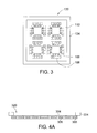
- FIG. 3 shows a top view of the semiconductor device carrier of FIG. 1J ;
- FIG. 4A shows a cross-sectional view of a semiconductor device carrier according to another embodiment of the invention.
- FIG. 4B shows a top view of the semiconductor device carrier of FIG. 4A .
- FIGS. 1A ⁇ 1J illustrates the processes of manufacturing a semiconductor device carrier according to an embodiment of the invention.
- a conductive carrier 102 having a first surface 102 a and a second surface 102 b opposite to the first surface 102 a is provided, wherein the conductive carrier 102 is preferably formed by a metal plate comprising of copper, iron or steel.
- a conductive trace layer 104 is formed on the second surface 102 b of the conductive carrier 102 preferably by means of photolithography and electrolytic plating.
- the conductive trace layer 104 is patterned to comprise of at least a trace 106 and at least a die pad 108 , and preferably formed by metal layers comprising of copper.
- a conductive stud layer is formed on the conductive trace layer 104 preferably by means of photolithography and electrolytic plating.
- the conductive stud layer comprises of at least a conductive stud 110 connected to the corresponding trace 106 and die pad 108 , and preferably formed by a metal such as copper.
- a first dielectric layer 112 is preferably formed by transfer molding to encapsulate the conductive trace layer 104 , the conductive stud layer and the second surface 102 b .
- the first dielectric layer 112 completely encapsulates the conductive trace layer 104 and the conductive stud layer.
- the first dielectric layer 112 is preferably formed by a material comprising of novolac-based resin, epoxy-based resin, silicone-based resin or other suitable encapsulant. The material is first heated to a molten state to encapsulate the conductive trace layer 104 and the conductive stud layer under a high-temperature and high-pressure environment and thereafter solidifies to form the first dielectric layer 112 .
- the first dielectric layer 112 also comprises of a suitable filler material such as powdered silicon dioxide.
- Exemplary steps for forming a first dielectric layer 112 are as follows. Firstly, an encapsulant comprising of resin and powdered silicon dioxide is provided and heated to a molten state. Next, the molten encapsulant is infused onto the second surface 102 b of the conductive carrier 102 and simultaneously envelops the conductive trace layer 104 and the conductive stud layer (including at least a conductive stud 110 ) under a high-temperature and high-pressure environment. Thereafter the encapsulant is solidified to form the first dielectric layer 112 .
- the first dielectric layer 112 can also be formed by injection molding or compression molding.
- an adhesion layer (not illustrated) is formed on the surface of the conductive trace layer 104 and the surface of the conductive stud layer to enhance the adhesion between these surfaces and the first dielectric layer 112 and increase the reliability of the product accordingly.
- a partial layer of the first dielectric layer 112 is removed preferably by grinding to expose a base surface 110 b of an end 110 a of the conductive stud 110 .
- a first dielectric surface 112 a is formed on the first dielectric layer 112
- the base surface 110 b is formed on the conductive stud 110 .
- the base surface 110 b of the conductive stud 110 is substantially aligned with (such as coplanar with) the first dielectric surface 112 a .
- the base surface 110 b of the end 110 a of the conductive stud 110 is exposed simultaneously when the first dielectric layer 112 is formed, such that subsequent removal of any partial layer of the first dielectric layer 112 is not required.
- a plating conductive layer 114 is formed to completely envelop the conductive carrier 102 , the first dielectric layer 112 and the exposed end 110 a of the conductive stud 110 .
- the plating conductive layer 114 is formed by electroless plating and enveloped the first surface 102 a , the lateral side 102 c and any exposed second surface 102 b of the conductive carrier 102 , the first dielectric surface 112 a and the lateral side 112 b of the first dielectric layer 112 , as well as the exposed end 110 a of the conductive stud 110 .
- the thickness of the plating conductive layer 114 ranges between 6 ⁇ 10 ⁇ m.
- the plating conductive layer 114 is preferably formed by a single-layered metal comprising of copper or nickel.
- the plating conductive layer 114 can also be formed by multi-layered metals.
- the formation of the conductive layer 114 comprises of the following steps. Firstly, a seed layer (not illustrated) is formed by electroless plating to envelop the conductive carrier 102 , the first dielectric layer 112 and the exposed end 110 a of the conductive stud 110 . The area encapsulated by the seed layer is similar to that encapsulated by the plating conductive layer 114 as described above.
- both the seed layer and sub-conductive layer comprises of copper or nickel respectively.
- the thickness of the seed layer ranges between 1 ⁇ 2 ⁇ m, and the thickness of the sub-conductive layer ranges between 5 ⁇ 8 ⁇ m.
- At least one cavity 116 is formed in the conductive carrier 102 wherein the conductive trace layer 104 and the first dielectric layer 112 are exposed in the cavity 116 .
- a portion of the conductive carrier 102 is removed by photolithography and etching to form the cavity 116 .
- the trace surface 104 a of the conductive trace layer 104 and the second dielectric surface 112 c of the first dielectric layer 112 are exposed from the cavity 116 , wherein the trace surface 104 a and the second dielectric surface 112 c are opposite to the first dielectric surface 112 a .
- the die pad 108 has a die pad surface 108 a and the trace 106 has a trace surface 106 a , wherein the die pad surface 108 a and the trace surface 106 a define the trace surface 104 a .
- the conductive trace layer 104 further comprises of an etching barrier layer (not illustrated) interposed between the conductive carrier 102 and the conductive trace layer 104 .
- the etching barrier layer comprises of nickel (Ni) or gold (Au).
- the remaining portion of the conductive carrier 102 forms a plating ring 134 around the peripheral of the first dielectric layer 112 .
- the plating ring 134 is electrically connected to the conductive stud 110 and the conductive trace layer 104 via the plating conductive layer 114 on the first dielectric surface 112 a.
- a first surface finishing 118 a is formed on the exposed conductive trace layer 104 .
- the first surface finishing 118 a is formed by electroplating on the entire trace surface 104 a of the conductive trace layer 104 exposed in the cavity 116 .
- the first surface finishing 118 a is formed on part of the trace surface 104 a of the conductive trace layer 104 exposed in the cavity 116 after photolithography.
- the first surface finishing 118 a is only formed on the trace surface 106 a of the trace 106 , but not on the die pad surface 108 a of the die pad 108 .
- the first surface finishing 118 a can further be formed on part of the trace surface 106 a of the trace 106 only.
- the first surface finishing 118 a is formed by electrolytic plating and comprises of nickel (Ni), palladium (Pa) or gold (Au).
- the plating conductive layer 114 electrically contacts the conductive stud 110 , such that the conductive trace layer 104 is electrically connected to the plating ring 134 via the conductive stud 110 and the plating conductive layer 114 .
- the plating ring 134 is subsequently connected to the electrode of the plating facility to allow electric current to flow through the plating conductive layer 114 for electroplating the first surface finishing 118 a on the conductive trace layer 104 .
- every trace 106 and every die pad 108 of the conductive layer 104 are isolated from one another by the first dielectric layer 112 (two neighboring traces are also isolated from each other).
- the plating conductive layer 114 electrically connects all the trace 106 and die pad 108 together such that the first surface finishing 118 a can be electroplated onto the conductive trace layer 104 simultaneously.
- the plating conductive layer 114 is subsequently removed preferably by etching to re-expose the base surface 110 b of the end 110 a of the conductive stud 110 and the first dielectric surface 112 a .
- every trace 106 and every die pad 108 of the conductive trace layer 104 are mutually isolated from one another and embedded in the first dielectric layer 112 respectively.
- a second surface finishing 118 b is thereafter formed on the exposed base surface 110 b of the end 110 a of the conductive stud 110 preferably by electroless plating.
- the formation of the semiconductor device carrier 120 of the present embodiment of the invention is completed.
- FIG. 3 a top view of the semiconductor device carrier of FIG. 1J is shown.
- the conductive trace layer 104 and the plating ring 134 are separated from each other by the first dielectric layer 112 , but such exemplification does not limit the invention.
- FIGS. 4A ⁇ 4B show a cross-sectional view of a semiconductor device carrier according to another embodiment of the invention.
- FIG. 4B shows a top view of the semiconductor device carrier of FIG. 4A .
- the conductive trace layer 304 of the semiconductor device carrier 320 is electrically connected to the plating ring 334 of the semiconductor device carrier 320 .
- every trace 306 and every die pad 308 of the conductive trace layer 104 are interconnected and further connected electrically to the plating ring 334 .
- the plating conductive layer 114 is completely removed, but such exemplification does not limit the invention, and the invention is further elaborated below by other examples.
- FIGS. 2A ⁇ 2B illustrates the processes of manufacturing a semiconductor device carrier according to another embodiment of the invention are shown.
- a portion of the plating conductive layer 114 is removed to form a remaining portion 114 a , wherein the remaining portion 114 a of the plating conductive layer 114 at least covers part of the conductive stud 110 .
- the remaining portion 114 a of the plating conductive layer 114 covers the entire base surface 110 b of the conductive stud 110 and also extends onto a portion of the first dielectric surface 112 a of the first dielectric layer 112 . Consequently, the area of the remaining portion 114 a of the plating conductive layer 114 is larger than that of the base surface 110 b of the conductive stud 110 .
- the remaining portion 114 a as an enlarged electrical pad (bond pad) can help to improve the electrical and assembly quality.
- the remaining portion 114 a of the plating conductive layer 114 only covers the base surface 110 b of the conductive stud 110 but not the first dielectric surface 112 a.
- a second surface finishing 118 b is subsequently formed on the remaining portion 114 a of the plating conductive layer 114 preferably by electroless plating.
- the remaining portion 114 a can also be considered as the second surface finishing 118 b and formed simultaneously when the plating conductive layer 114 is removed.
- the present embodiment of the invention does not require an additional manufacturing process for forming the second surface finishing 118 b on the base surface 110 b of the conductive stud 110 .
- the second surface finishing 118 b is also formed.
- the formation of the semiconductor device carrier 220 is completed.
- FIG. 1K to 1M illustrates the processes of manufacturing a semiconductor package using the semiconductor device carrier 220 .
- at least one semiconductor device 122 is disposed adjacent to the conductive trace layer 104 .
- the semiconductor device 122 has a rear surface 122 b and an active surface 122 a opposite to the rear surface 122 b .
- the rear surface 122 b of the semiconductor device 122 may be attached to the conductive trace layer 104 by means of an adhesive 128 .
- the face-up active surface 122 a of the semiconductor device 122 is electrically connected to the trace 106 via at least one bonding wire 124 by connecting to the first surface finishing 118 a of the trace 106 .
- the active surface of the semiconductor device 130 is in a face-down manner and several interconnections 132 are electrically connecting the semiconductor device 130 to at least one of the die pad 108 or the trace 106 via the first surface finishing 118 a .
- the semiconductor device 130 is a flip-chip.
- the interconnections 132 of the semiconductor device 130 bond directly onto at least one of the die pad 108 or the trace 106 .
- a second dielectric layer 126 is formed by molding to encapsulate the semiconductor device 122 and the bonding wire 124 .
- the second dielectric layer 126 and the first dielectric layer 112 are singulated by using a cutting tool or laser to separate the assembled semiconductor device carrier 120 .
- a cutting tool or laser to separate the assembled semiconductor device carrier 120 .
- the dielectric layer of the semiconductor device carrier encapsulates the conductive trace layer and the conductive stud layer which electrically connects the two opposite sides of the semiconductor device carrier. Since no through-hole is required and the dielectric layer has a smaller thickness, the size of the semiconductor package is thus effectively reduced. Furthermore, since the surface finishing on the mutually isolated traces and die pads of the conductive trace layer is formed by electrolytic plating, the stability and reliability of the product are further increased.
Landscapes
- Engineering & Computer Science (AREA)
- Microelectronics & Electronic Packaging (AREA)
- Computer Hardware Design (AREA)
- Power Engineering (AREA)
- Physics & Mathematics (AREA)
- Condensed Matter Physics & Semiconductors (AREA)
- General Physics & Mathematics (AREA)
- Electroplating Methods And Accessories (AREA)
- Structures Or Materials For Encapsulating Or Coating Semiconductor Devices Or Solid State Devices (AREA)
- Internal Circuitry In Semiconductor Integrated Circuit Devices (AREA)
- Led Device Packages (AREA)
Priority Applications (3)
| Application Number | Priority Date | Filing Date | Title |
|---|---|---|---|
| US13/222,792 US8709874B2 (en) | 2010-08-31 | 2011-08-31 | Manufacturing method for semiconductor device carrier and semiconductor package using the same |
| US14/185,779 US9219027B2 (en) | 2010-08-31 | 2014-02-20 | Semiconductor device carrier and semiconductor package using the same |
| US14/961,825 US9583449B2 (en) | 2010-08-31 | 2015-12-07 | Semiconductor package |
Applications Claiming Priority (2)
| Application Number | Priority Date | Filing Date | Title |
|---|---|---|---|
| US37844710P | 2010-08-31 | 2010-08-31 | |
| US13/222,792 US8709874B2 (en) | 2010-08-31 | 2011-08-31 | Manufacturing method for semiconductor device carrier and semiconductor package using the same |
Related Child Applications (1)
| Application Number | Title | Priority Date | Filing Date |
|---|---|---|---|
| US14/185,779 Division US9219027B2 (en) | 2010-08-31 | 2014-02-20 | Semiconductor device carrier and semiconductor package using the same |
Publications (2)
| Publication Number | Publication Date |
|---|---|
| US20120058604A1 US20120058604A1 (en) | 2012-03-08 |
| US8709874B2 true US8709874B2 (en) | 2014-04-29 |
Family
ID=45359400
Family Applications (3)
| Application Number | Title | Priority Date | Filing Date |
|---|---|---|---|
| US13/222,792 Active 2032-08-08 US8709874B2 (en) | 2010-08-31 | 2011-08-31 | Manufacturing method for semiconductor device carrier and semiconductor package using the same |
| US14/185,779 Active US9219027B2 (en) | 2010-08-31 | 2014-02-20 | Semiconductor device carrier and semiconductor package using the same |
| US14/961,825 Active US9583449B2 (en) | 2010-08-31 | 2015-12-07 | Semiconductor package |
Family Applications After (2)
| Application Number | Title | Priority Date | Filing Date |
|---|---|---|---|
| US14/185,779 Active US9219027B2 (en) | 2010-08-31 | 2014-02-20 | Semiconductor device carrier and semiconductor package using the same |
| US14/961,825 Active US9583449B2 (en) | 2010-08-31 | 2015-12-07 | Semiconductor package |
Country Status (3)
| Country | Link |
|---|---|
| US (3) | US8709874B2 (zh) |
| CN (2) | CN103824836B (zh) |
| TW (2) | TWI543327B (zh) |
Cited By (2)
| Publication number | Priority date | Publication date | Assignee | Title |
|---|---|---|---|---|
| US20150279777A1 (en) * | 2014-03-28 | 2015-10-01 | Phoenix Pioneer Technology Co., Ltd. | Package apparatus and manufacturing method thereof |
| US10319684B2 (en) | 2017-04-11 | 2019-06-11 | STATS ChipPAC Pte. Ltd. | Dummy conductive structures for EMI shielding |
Families Citing this family (20)
| Publication number | Priority date | Publication date | Assignee | Title |
|---|---|---|---|---|
| CN103066051B (zh) * | 2011-10-20 | 2017-03-01 | 先进封装技术私人有限公司 | 封装基板及其制作工艺、半导体元件封装结构及制作工艺 |
| TWI557855B (zh) * | 2011-12-30 | 2016-11-11 | 旭德科技股份有限公司 | 封裝載板及其製作方法 |
| JP6436396B2 (ja) * | 2012-03-26 | 2018-12-12 | アドヴァンパック ソリューションズ ピーティーイー リミテッド | 半導体パッケージング用の多層基板および多層基板を製造する方法 |
| US8587099B1 (en) * | 2012-05-02 | 2013-11-19 | Texas Instruments Incorporated | Leadframe having selective planishing |
| US10991669B2 (en) | 2012-07-31 | 2021-04-27 | Mediatek Inc. | Semiconductor package using flip-chip technology |
| TWI562295B (en) | 2012-07-31 | 2016-12-11 | Mediatek Inc | Semiconductor package and method for fabricating base for semiconductor package |
| US9177899B2 (en) | 2012-07-31 | 2015-11-03 | Mediatek Inc. | Semiconductor package and method for fabricating base for semiconductor package |
| US20160056098A9 (en) * | 2012-09-28 | 2016-02-25 | Yan Xun Xue | Semiconductor device employing aluminum alloy lead-frame with anodized aluminum |
| TWI471990B (zh) * | 2012-11-05 | 2015-02-01 | 矽品精密工業股份有限公司 | 用於固定半導體封裝件之承載件與半導體封裝件之製法 |
| WO2014112954A1 (en) * | 2013-01-21 | 2014-07-24 | Pbt Pte. Ltd. | Substrate for semiconductor packaging and method of forming same |
| SG10201708630YA (en) | 2013-02-21 | 2017-12-28 | Advanpack Solutions Pte Ltd | Semiconductor structure and method of fabricating the same |
| CN104064542B (zh) * | 2013-03-21 | 2018-04-27 | 新科金朋有限公司 | 无核心集成电路封装系统及其制造方法 |
| US9142530B2 (en) | 2013-03-21 | 2015-09-22 | Stats Chippac Ltd. | Coreless integrated circuit packaging system and method of manufacture thereof |
| US9257370B2 (en) * | 2013-08-27 | 2016-02-09 | Ubotic Company Limited | Cavity package with pre-molded cavity leadframe |
| CN104425392A (zh) | 2013-08-27 | 2015-03-18 | 优博创新科技有限公司 | 具有预模制的基板的空腔封装 |
| TWI581386B (zh) * | 2014-06-16 | 2017-05-01 | 恆勁科技股份有限公司 | 封裝裝置及其製作方法 |
| TWI474417B (zh) * | 2014-06-16 | 2015-02-21 | Phoenix Pioneer Technology Co Ltd | 封裝方法 |
| TWI591762B (zh) * | 2014-06-30 | 2017-07-11 | 恆勁科技股份有限公司 | 封裝裝置及其製作方法 |
| US20160099200A1 (en) * | 2014-10-01 | 2016-04-07 | Stmicroelectronics S.R.L. | Aluminum alloy lead frame for a semiconductor device and corresponding manufacturing process |
| TWI569368B (zh) | 2015-03-06 | 2017-02-01 | 恆勁科技股份有限公司 | 封裝基板、包含該封裝基板的封裝結構及其製作方法 |
Citations (5)
| Publication number | Priority date | Publication date | Assignee | Title |
|---|---|---|---|---|
| US20060094158A1 (en) * | 2004-10-28 | 2006-05-04 | Samsung Electronics Co., Ltd. | Fabrication method of packaging substrate and packaging method using the packaging substrate |
| US7790505B2 (en) * | 2006-10-18 | 2010-09-07 | Advanced Semiconductor Engineering, Inc. | Semiconductor chip package manufacturing method and structure thereof |
| US7915080B2 (en) * | 2008-12-19 | 2011-03-29 | Texas Instruments Incorporated | Bonding IC die to TSV wafers |
| US8159828B2 (en) * | 2007-02-23 | 2012-04-17 | Alpha & Omega Semiconductor, Inc. | Low profile flip chip power module and method of making |
| US8338232B2 (en) * | 2010-12-28 | 2012-12-25 | Alpha & Omega Semiconductor, Inc. | Power semiconductor device package method |
Family Cites Families (14)
| Publication number | Priority date | Publication date | Assignee | Title |
|---|---|---|---|---|
| US5976912A (en) * | 1994-03-18 | 1999-11-02 | Hitachi Chemical Company, Ltd. | Fabrication process of semiconductor package and semiconductor package |
| JP2581017B2 (ja) * | 1994-09-30 | 1997-02-12 | 日本電気株式会社 | 半導体装置及びその製造方法 |
| KR100218996B1 (ko) * | 1995-03-24 | 1999-09-01 | 모기 쥰이찌 | 반도체장치 |
| JP3264147B2 (ja) * | 1995-07-18 | 2002-03-11 | 日立電線株式会社 | 半導体装置、半導体装置用インターポーザ及びその製造方法 |
| JP3176542B2 (ja) * | 1995-10-25 | 2001-06-18 | シャープ株式会社 | 半導体装置及びその製造方法 |
| EP0791960A3 (en) * | 1996-02-23 | 1998-02-18 | Matsushita Electric Industrial Co., Ltd. | Semiconductor devices having protruding contacts and method for making the same |
| JP3437369B2 (ja) * | 1996-03-19 | 2003-08-18 | 松下電器産業株式会社 | チップキャリアおよびこれを用いた半導体装置 |
| US6064111A (en) * | 1996-07-31 | 2000-05-16 | Hitachi Company, Ltd. | Substrate for holding a chip of semi-conductor package, semi-conductor package, and fabrication process of semi-conductor package |
| US6060777A (en) * | 1998-07-21 | 2000-05-09 | Intel Corporation | Underside heat slug for ball grid array packages |
| TW473962B (en) * | 2001-01-20 | 2002-01-21 | Siliconware Precision Industries Co Ltd | Cavity down ball grid array package and its manufacturing process |
| US7259448B2 (en) * | 2001-05-07 | 2007-08-21 | Broadcom Corporation | Die-up ball grid array package with a heat spreader and method for making the same |
| US6537848B2 (en) * | 2001-05-30 | 2003-03-25 | St. Assembly Test Services Ltd. | Super thin/super thermal ball grid array package |
| US6879039B2 (en) * | 2001-12-18 | 2005-04-12 | Broadcom Corporation | Ball grid array package substrates and method of making the same |
| US6861750B2 (en) * | 2002-02-01 | 2005-03-01 | Broadcom Corporation | Ball grid array package with multiple interposers |
-
2011
- 2011-08-31 TW TW102144935A patent/TWI543327B/zh active
- 2011-08-31 CN CN201410059244.7A patent/CN103824836B/zh active Active
- 2011-08-31 CN CN201110255914.9A patent/CN102299082B/zh active Active
- 2011-08-31 TW TW100131282A patent/TWI429048B/zh active
- 2011-08-31 US US13/222,792 patent/US8709874B2/en active Active
-
2014
- 2014-02-20 US US14/185,779 patent/US9219027B2/en active Active
-
2015
- 2015-12-07 US US14/961,825 patent/US9583449B2/en active Active
Patent Citations (5)
| Publication number | Priority date | Publication date | Assignee | Title |
|---|---|---|---|---|
| US20060094158A1 (en) * | 2004-10-28 | 2006-05-04 | Samsung Electronics Co., Ltd. | Fabrication method of packaging substrate and packaging method using the packaging substrate |
| US7790505B2 (en) * | 2006-10-18 | 2010-09-07 | Advanced Semiconductor Engineering, Inc. | Semiconductor chip package manufacturing method and structure thereof |
| US8159828B2 (en) * | 2007-02-23 | 2012-04-17 | Alpha & Omega Semiconductor, Inc. | Low profile flip chip power module and method of making |
| US7915080B2 (en) * | 2008-12-19 | 2011-03-29 | Texas Instruments Incorporated | Bonding IC die to TSV wafers |
| US8338232B2 (en) * | 2010-12-28 | 2012-12-25 | Alpha & Omega Semiconductor, Inc. | Power semiconductor device package method |
Cited By (4)
| Publication number | Priority date | Publication date | Assignee | Title |
|---|---|---|---|---|
| US20150279777A1 (en) * | 2014-03-28 | 2015-10-01 | Phoenix Pioneer Technology Co., Ltd. | Package apparatus and manufacturing method thereof |
| US9750142B2 (en) * | 2014-03-28 | 2017-08-29 | Phoenix Pioneer Technology Co., Ltd. | Method for manufacturing an electronic package |
| US11246223B2 (en) | 2014-03-28 | 2022-02-08 | Phoenix Pioneer Technology Co., Ltd. | Package apparatus |
| US10319684B2 (en) | 2017-04-11 | 2019-06-11 | STATS ChipPAC Pte. Ltd. | Dummy conductive structures for EMI shielding |
Also Published As
| Publication number | Publication date |
|---|---|
| US9583449B2 (en) | 2017-02-28 |
| US20140167240A1 (en) | 2014-06-19 |
| CN103824836A (zh) | 2014-05-28 |
| TWI543327B (zh) | 2016-07-21 |
| CN103824836B (zh) | 2017-03-01 |
| TW201419486A (zh) | 2014-05-16 |
| CN102299082A (zh) | 2011-12-28 |
| CN102299082B (zh) | 2014-04-16 |
| TWI429048B (zh) | 2014-03-01 |
| TW201209983A (en) | 2012-03-01 |
| US20120058604A1 (en) | 2012-03-08 |
| US9219027B2 (en) | 2015-12-22 |
| US20160118349A1 (en) | 2016-04-28 |
Similar Documents
| Publication | Publication Date | Title |
|---|---|---|
| US8709874B2 (en) | Manufacturing method for semiconductor device carrier and semiconductor package using the same | |
| US11355449B2 (en) | Semiconductor device having EMI shielding structure and related methods | |
| CN107017238B (zh) | 电子装置 | |
| US10566271B2 (en) | Carrier-free semiconductor package and fabrication method | |
| TWI527175B (zh) | 半導體封裝件、基板及其製造方法 | |
| CN108063094A (zh) | 基于基板的扇出型晶圆级封装 | |
| TW200818458A (en) | Stackable packages for three-dimensional packaging of semiconductor dice | |
| US20120104607A1 (en) | Stacked semiconductor packages and related methods | |
| CN111293112B (zh) | 半导体封装和其制造方法 | |
| US9112063B2 (en) | Fabrication method of semiconductor package | |
| US20160155716A1 (en) | Package substrate, semiconductor package and method of manufacturing the same | |
| TW201705426A (zh) | 樹脂密封型半導體裝置及其製造方法 | |
| TWI596731B (zh) | 使用無電鍍之z型連接 | |
| US7868449B2 (en) | Semiconductor substrate and method of connecting semiconductor die to substrate | |
| KR20090096184A (ko) | 반도체 패키지 | |
| CN100395888C (zh) | 半导体封装件及其制法 | |
| US20240120262A1 (en) | Semiconductor devices and methods of manufacturing semiconductor devices | |
| CN107978584B (zh) | 芯片封装结构及其制造方法 | |
| US20230110079A1 (en) | Fan-out package structure and manufacturing method thereof | |
| KR20240057505A (ko) | 반도체 디바이스의 제조 방법 및 이에 따른 반도체 디바이스 | |
| US9029198B2 (en) | Methods of manufacturing semiconductor devices including terminals with internal routing interconnections | |
| TW202027243A (zh) | 封裝結構及其製造方法 | |
| JP2010187037A (ja) | 半導体装置の製造方法 | |
| TWI456718B (zh) | 封裝結構及其製法 |
Legal Events
| Date | Code | Title | Description |
|---|---|---|---|
| AS | Assignment |
Owner name: ADVANPACK SOLUTIONS PTE LTD., SINGAPORE Free format text: ASSIGNMENT OF ASSIGNORS INTEREST;ASSIGNORS:CHEW, HWEE-SENG JIMMY;LIM, KIAN-HOCK;FORTALEZA, OVISO DOMINADOR JR;AND OTHERS;REEL/FRAME:026839/0780 Effective date: 20110824 |
|
| STCF | Information on status: patent grant |
Free format text: PATENTED CASE |
|
| MAFP | Maintenance fee payment |
Free format text: PAYMENT OF MAINTENANCE FEE, 4TH YR, SMALL ENTITY (ORIGINAL EVENT CODE: M2551) Year of fee payment: 4 |
|
| MAFP | Maintenance fee payment |
Free format text: PAYMENT OF MAINTENANCE FEE, 8TH YR, SMALL ENTITY (ORIGINAL EVENT CODE: M2552); ENTITY STATUS OF PATENT OWNER: SMALL ENTITY Year of fee payment: 8 |