US8102186B2 - Semiconductor integrated circuit with first and second transmitter-receivers - Google Patents
Semiconductor integrated circuit with first and second transmitter-receivers Download PDFInfo
- Publication number
- US8102186B2 US8102186B2 US12/876,747 US87674710A US8102186B2 US 8102186 B2 US8102186 B2 US 8102186B2 US 87674710 A US87674710 A US 87674710A US 8102186 B2 US8102186 B2 US 8102186B2
- Authority
- US
- United States
- Prior art keywords
- data
- transmitter
- receiver
- switch
- circuit
- Prior art date
- Legal status (The legal status is an assumption and is not a legal conclusion. Google has not performed a legal analysis and makes no representation as to the accuracy of the status listed.)
- Active
Links
Images


Classifications
-
- G—PHYSICS
- G11—INFORMATION STORAGE
- G11C—STATIC STORES
- G11C11/00—Digital stores characterised by the use of particular electric or magnetic storage elements; Storage elements therefor
- G11C11/21—Digital stores characterised by the use of particular electric or magnetic storage elements; Storage elements therefor using electric elements
- G11C11/34—Digital stores characterised by the use of particular electric or magnetic storage elements; Storage elements therefor using electric elements using semiconductor devices
- G11C11/40—Digital stores characterised by the use of particular electric or magnetic storage elements; Storage elements therefor using electric elements using semiconductor devices using transistors
- G11C11/401—Digital stores characterised by the use of particular electric or magnetic storage elements; Storage elements therefor using electric elements using semiconductor devices using transistors forming cells needing refreshing or charge regeneration, i.e. dynamic cells
- G11C11/4063—Auxiliary circuits, e.g. for addressing, decoding, driving, writing, sensing or timing
- G11C11/407—Auxiliary circuits, e.g. for addressing, decoding, driving, writing, sensing or timing for memory cells of the field-effect type
- G11C11/4074—Power supply or voltage generation circuits, e.g. bias voltage generators, substrate voltage generators, back-up power, power control circuits
-
- G—PHYSICS
- G11—INFORMATION STORAGE
- G11C—STATIC STORES
- G11C11/00—Digital stores characterised by the use of particular electric or magnetic storage elements; Storage elements therefor
- G11C11/21—Digital stores characterised by the use of particular electric or magnetic storage elements; Storage elements therefor using electric elements
- G11C11/34—Digital stores characterised by the use of particular electric or magnetic storage elements; Storage elements therefor using electric elements using semiconductor devices
- G11C11/40—Digital stores characterised by the use of particular electric or magnetic storage elements; Storage elements therefor using electric elements using semiconductor devices using transistors
- G11C11/41—Digital stores characterised by the use of particular electric or magnetic storage elements; Storage elements therefor using electric elements using semiconductor devices using transistors forming static cells with positive feedback, i.e. cells not needing refreshing or charge regeneration, e.g. bistable multivibrator or Schmitt trigger
- G11C11/413—Auxiliary circuits, e.g. for addressing, decoding, driving, writing, sensing, timing or power reduction
- G11C11/417—Auxiliary circuits, e.g. for addressing, decoding, driving, writing, sensing, timing or power reduction for memory cells of the field-effect type
- G11C11/419—Read-write [R-W] circuits
-
- G—PHYSICS
- G11—INFORMATION STORAGE
- G11C—STATIC STORES
- G11C7/00—Arrangements for writing information into, or reading information out from, a digital store
- G11C7/02—Arrangements for writing information into, or reading information out from, a digital store with means for avoiding parasitic signals
-
- G—PHYSICS
- G11—INFORMATION STORAGE
- G11C—STATIC STORES
- G11C7/00—Arrangements for writing information into, or reading information out from, a digital store
- G11C7/22—Read-write [R-W] timing or clocking circuits; Read-write [R-W] control signal generators or management
-
- H—ELECTRICITY
- H03—ELECTRONIC CIRCUITRY
- H03K—PULSE TECHNIQUE
- H03K19/00—Logic circuits, i.e. having at least two inputs acting on one output; Inverting circuits
- H03K19/0005—Modifications of input or output impedance
-
- H—ELECTRICITY
- H03—ELECTRONIC CIRCUITRY
- H03K—PULSE TECHNIQUE
- H03K19/00—Logic circuits, i.e. having at least two inputs acting on one output; Inverting circuits
- H03K19/0175—Coupling arrangements; Interface arrangements
- H03K19/017545—Coupling arrangements; Impedance matching circuits
Definitions
- the present invention relates to a semiconductor integrated circuit, and more particularly, to a semiconductor integrated circuit suitable for power-supply noise reduction.
- a countermeasure for example, ODT (On Die Termination) technique has been provided to reduce the power-supply noise on signal lines used for data reception of transmitter-receivers (JEDEC STANDARD, DDR2 SDRAM SPECIFICATION JESD79-2L (Revision of JESD79-2D), April 2008, JEDEC SOLID STATE TECHNOLOGY ASSOCIATION).
- a bidirectional signal line for bidirectionally transmitting data between the transmitter-receivers is equipped with a termination circuit which switches on an ODT function when receiving the data and switches off the ODT function when not receiving the data in each transmitter-receiver.
- the power-supply noise occurs on the bidirectional signal line due to a sudden fluctuation of a power supply voltage when the receiver circuit, which is a data receiving side, switches off the ODT function after receiving data.
- the receiver circuit switches the ODT function from the off-state to the on-state to receive another data before the power-supply noise converges, another data is influenced by the power-supply noise.
- the present inventors have found a problem in the related art that, as described above, it is impossible to execute transmission and reception of data accurately.
- a first exemplary aspect of the present invention is a semiconductor integrated circuit including:
- the first transmitter-receiver includes:
- FIG. 1 illustrates a semiconductor integrated circuit according to a first exemplary embodiment of the present invention
- FIG. 2 illustrates the semiconductor integrated circuit according to the first exemplary embodiment of the present invention
- FIG. 3 is a timing chart depicting an operation of the semiconductor integrated circuit according to the first exemplary embodiment of the present invention.
- FIG. 4 illustrates a semiconductor integrated circuit according to a second exemplary embodiment of the present invention.
- the present invention can be applied to a circuit which includes a first transmitter-receiver, a second transmitter-receiver, and a signal line for bidirectionally transmitting data between the first transmitter-receiver and the second transmitter-receiver (hereinafter, referred to simply as “bidirectional signal line”), and has an ODT function.
- a case is explained hereinafter in which the circuit shown in FIG. 1 includes an SoC (System on Chip) circuit and an SDRAM (Synchronous Dynamic Random Access Memory) circuit, and data transmission is executed between the SoC circuit and the SDRAM circuit through the bidirectional signal line.
- SoC System on Chip
- SDRAM Synchronous Dynamic Random Access Memory
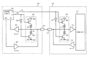
- FIG. 1 illustrates a semiconductor integrated circuit according to the first exemplary embodiment of the present invention.
- the circuit shown in FIG. 1 includes an SoC circuit (first transmitter-receiver) 100 and an SDRAM circuit (second transmitter-receiver) 101 .
- Data transmission is executed between the SoC circuit 100 and the SDRAM circuit 101 in the DDR (double data rate) mode.
- DDR double data rate
- the SoC circuit 100 outputs a 2-bit clock signal CK and a 2-bit clock signal CKB, which is a differential signal of the clock signal CK, to the SDRAM circuit 101 .
- the SoC circuit 100 further outputs a 16-bit control signal CMD, which includes commands for each address of the SDRAM circuit 101 , to the SDRAM circuit 101 .
- the SDRAM circuit 101 receives the control signal CMD in synchronization with the clock signals CK and CKB.
- a receiver circuit which is one of the SoC circuit 100 and the SDRAM circuit 101 , receives the data DC) in synchronization with the strobe signals DQS and DQSB.
- the signal names described above also represent the corresponding signal line names.
- the circuit shown in FIG. 2 shows a 1-bit bidirectional signal line, which is one of strobe signal lines DQS[3:0] and DQSB[3:0] and a data signal line DQ[31:0], and corresponding peripheral circuits of the circuit shown in FIG. 1 .
- the 1-bit bidirectional signal line is the data signal line DQ[0].
- the data signal line DQ[0] is connected between the SoC circuit 100 and the SDRAM 101 as described above.
- the SoC circuit 100 includes an external terminal 201 , a buffer 202 , a buffer 203 , a termination circuit (first termination circuit) 204 which has an ODT function, a control circuit 205 which outputs a control signal (first control signal) 200 to control the ODT function of the termination circuit 204 to be turned on and off, and an inverter 206 .
- the termination circuit 204 includes a resistor (first resistor) 207 , a resistor 208 , a switch (first switch) 209 , and a switch 210 .
- the switch 209 is a P-channel MOS transistor and the switch 210 is an N-channel MOS transistor.
- the data signal line DQ[0] is connected to an input terminal of the buffer 202 and an output terminal of the buffer 203 through the external terminal 201 .
- the termination circuit 204 is provided between the external terminal 201 and the buffer 202 .
- the switch 209 and the resistor 207 are connected in series between a high potential side power supply terminal VDD and a node N 1 which is located on the signal line connecting the external terminal 201 and the buffer 202 .
- the switch 210 and the resistor 208 are connected in series between a low potential side power supply terminal VSS and the node N 1 .
- the source terminal of the switch 209 is connected to the high potential side power supply terminal VDD.
- the drain terminal of the switch 209 is connected to one terminal of the resistor 207 .
- the other terminal of the resistor 207 is connected to one terminal of the resistor 208 .
- the other terminal of the resistor 208 is connected to the drain terminal of the switch 210 .
- the source terminal of the switch 210 is connected to the low potential side power supply terminal VSS.
- the other terminal of the resistor 207 and one terminal of the resistor 208 are commonly connected to the node N 1 .
- the switch 209 and the resistor 207 which are connected in series between the high potential side power supply terminal VDD and the node N 1 may be switched around.
- the switch 210 and the resistor 208 which are connected in series between the low potential side power supply terminal VSS and the node N 1 may be switched around.
- An output terminal of the buffer 202 is connected to an input terminal IN of the control circuit 205 .
- An input terminal of the buffer 203 is connected to an output terminal OUT of the control circuit 205 .
- An output terminal C 1 of the control circuit 205 is connected to the gate terminal of the switch 209 and the gate terminal of the switch 210 through the inverter 206 .
- Such a peripheral circuit configuration is also employed in the other bidirectional signal lines. Note that the control circuit 205 is commonly provided to these bidirectional signal lines.
- the SoC circuit 100 receives (reads) the data such as the data DQ and the strobe signals DQS and DQSB transmitted from the SDRAM circuit 101 .
- the SoC circuit 100 outputs the control signal CMD to the SDRAM circuit 101 .
- the SDRAM circuit 101 transmits the data DQ stored in a memory area of an address specified by the control signal CMD, and the strobe signals DQS and DQSB to the SoC circuit 100 .
- the data DQ transmitted from the SDRAM circuit 101 has a predetermined burst length.
- the SoC circuit 100 receives each signal output from the SDRAM circuit 101 through the corresponding signal line, external terminal 201 , and buffer 202 . Note that the SoC circuit 100 receives the data DQ in synchronization with the strobe signals DQS and DQSB. The data DQ received by the SoC circuit 100 is input to the control circuit 205 and the other peripheral circuits (not shown). A period between the time when the SoC circuit 100 starts to transmit the control signal CMD and the time when SoC circuit 100 starts to receive the corresponding data DQ is called a read latency (RL).
- RL read latency
- the SoC circuit 100 controls the ODT function of the corresponding termination circuit 204 to be turned on to reduce power-supply noise occurring on the data signal line DQ and the strobe signal lines DQS and DQSB. Specifically, the SoC circuit 100 controls the switches 209 and 210 , which are provided in the corresponding termination circuit 204 , to be turned on based on the control signal (first control signal) 200 from the control circuit 205 and sets the node on the corresponding signal line to a predetermined potential (for example, one-half of the high potential side power supply voltage VDD). This makes it possible for the SoC circuit 100 to receive the data accurately by reducing the power-supply noise included in the received data.
- a predetermined potential for example, one-half of the high potential side power supply voltage VDD
- the SoC circuit 100 transmits (writes) the data to the SDRAM circuit 101 .
- the SoC circuit 100 outputs the control signal CMD to the SDRAM circuit 101 .
- the SoC circuit 100 transmits the data DO and the strobe signals DQS and DQSB to the SDRAM circuit 101 .
- the data DQ transmitted from the SoC circuit 100 has a predetermined burst length.
- the SDRAM circuit 101 receives the data DQ in synchronization with the strobe signals DQS and DQSB.
- the data DQ is written into the memory area of the address specified by the control signal CMD.
- a period between the time when the SoC circuit 100 starts to transmit the control signal CMD and the time when the SoC circuit 100 starts to transmit the corresponding data DQ is called a write latency (WL).
- the SoC circuit 100 controls the ODT function of the corresponding termination circuit 204 to be turned off. Specifically, the SoC circuit 100 controls the switches 209 and 210 , which are provided in the corresponding termination circuit 204 , to be turned off based on the control signal 200 from the control circuit 205 , thereby preventing the potential of the data transmitted to the SDRAM circuit 101 through the buffer 203 and the external terminal 201 from being decayed. This makes it possible for the SoC circuit 100 to transmit the data accurately.
- the SoC circuit 100 switches between a read mode in which the SoC circuit 100 receives the data transmitted from the SDRAM circuit 101 and a write mode in which the SoC circuit 100 transmits the data to the SDRAM circuit 101 , based on the control signal CMD.
- the SoC circuit 100 outputs the control signal CMD which has a data length corresponding to one cycle of the clock signal CK at predetermined time intervals.
- the SoC circuit 100 receives data such as the data DQ in the read mode or transmits the data in the write mode, and after the predetermined time interval, receives or transmits another data in the same mode.
- the SoC circuit 100 receives data such as the data DQ in the read mode or transmits the data in the write mode, and after the predetermined time interval, receives or transmits another data in a different mode. The data transmission and reception as described above is repeated.
- the SoC circuit 100 exhibits characteristics when the SoC circuit 100 receives data such as the data DQ in the read mode, and after the predetermined time interval, receives another data in the read mode again.
- the operation of the SoC circuit 100 in this case will be described with reference to FIG. 3 .
- the SoC circuit 100 outputs the control signal CMD (which is indicated by “A” shown in FIG. 3 and is hereinafter referred to as “read command A”) to the SDRAM circuit 101 . Then, the SDRAM circuit 101 transmits the data DQ (“D” shown in FIG. 3 ), which has a predetermined burst length, and the corresponding strobe signals DQS and DQSB to the SoC circuit 100 after the period of the read latency RL (“C” shown in FIG. 3 ).
- the SoC circuit 100 controls the ODT function of the corresponding termination circuit 204 to be turned on.
- the SoC circuit 100 After outputting the read command A, the SoC circuit 100 outputs a read command E (“E” shown in FIG. 3 ) after the period of the predetermined time interval (“B” shown in FIG. 3 ).
- the SDRAM circuit 101 transmits the data DQ (“G” shown in FIG. 3 ), which has a predetermined burst length, and the corresponding strobe signals DQS and DQSB to the SoC circuit 100 after the period of the read latency RL (“F” shown in FIG. 3 )
- the control circuit 205 provided in the SoC circuit 100 calculates a period (H), in which the data DQ is not transmitted, based on the interval (B) of the read commands (A, E), the read latency RL (C, F), and the burst length (D, G) of the data DQ. Based on the period thus obtained, the control circuit 205 determines whether to turn off the ODT function of the termination circuit 204 during the period (H) in which the data DQ is not transmitted. Then, the control circuit 205 outputs the control signal 200 to the termination circuit 204 based on the results of the determination.
- the termination circuit 204 When the period (H) is less than or equal to a predetermined threshold, the termination circuit 204 causes the ODT function to be continuously on during the period (H) (“I” shown in FIG. 3 ). When the period (H) exceeds the predetermined threshold, the termination circuit 204 switches off the ODT function during the period (H).
- the termination circuit 204 causes the ODT function to be continuously on during the period in which the data transmission is not executed, power-supply noise, which may occur due to switching from the on-state to the off-state of the ODT function, does not occur on the bidirectional signal line corresponding to the termination circuit 204 . Therefore, it is possible for the SoC circuit 100 to receive the data accurately by reducing the power-supply noise which has been a problem in the related art.
- the termination circuit 204 switches the ODT function from the on-state to the off-state during the period in which the data transmission is not executed.
- the SoC circuit 100 can control the ODT function of the termination circuit 204 to be switched from the off-state to the on-state again after a lapse of a period sufficient for converging the power-supply noise due to switching from the on-state to the off-state of the ODT function. This makes it possible for the SoC circuit 100 to receive the data accurately by reducing the effect of the power-supply noise.
- the timing of switching from the on-state to the off-state of the ODT function may be arbitrarily determined as long as the power-supply noise is converged by the time when the next data reception starts.
- the semiconductor integrated circuit according to this exemplary embodiment of the present invention controls the ODT function of the receiver circuit to be turned on and off based on a data reception interval.
- the semiconductor integrated circuit according to this exemplary embodiment controls the ODT function of the receiver circuit to be continuously on or to be switched from the on-state to the off-state. This makes it possible for the semiconductor integrated circuit according to this exemplary embodiment to execute transmission and reception of data accurately by reducing the effect of the power-supply noise.
- the case has been explained in which the SoC circuit 100 includes the termination circuit 204 . Meanwhile, in this exemplary embodiment, a case is explained in which an SDRAM circuit also includes a termination circuit.
- an SDRAM circuit 102 which corresponds to the SDRAM circuit 101 shown in FIG. 2 further includes a termination circuit (second termination circuit) 215 .
- FIG. 4 shows the 1-bit bidirectional signal line, which is one of the strobe signal lines DQS[3:0] and DQSB[3:0] and the data signal line DQ[31:0], and the corresponding peripheral circuits.
- the circuit shown in FIG. 4 includes the SoC circuit 100 and the SDRAM circuit 102 .
- the SDRAM circuit 102 includes an SDRAM unit 211 , an external terminal 212 , a buffer 213 , a buffer 214 , a termination circuit 215 , and an inverter 216 .
- the termination circuit 215 includes a resistor (second resistor) 217 , a resistor 218 , a switch (second switch) 219 , and a switch 220 .
- the circuit structure and the operation of the SoC circuit 100 are the same as those of the first exemplary embodiment, so the description thereof is omitted. As for the connections and the operations of circuits which are associated with the ODT function and provided in the SDRAM circuit 102 , only different contents from those of the SoC circuit 100 will be described.
- the SDRAM circuit 102 controls the ODT function of the corresponding termination circuit 215 to be turned on to reduce the power-supply noise occurring on the data signal line DQ and the strobe signal lines DOS and DQSB. Specifically, the SDRAM circuit 102 controls the switches 219 and 220 , which are provided in the corresponding termination circuit 215 , to be turned on based on a control signal (second control signal) 221 from the control circuit 205 and sets the node on the corresponding signal line to the predetermined potential (for example, one-half of the high potential side power supply terminal VDD). This makes is possible for the SDRAM circuit 102 to receive the data accurately by reducing the power-supply noise included in the received data.
- a control signal second control signal
- the SDRAM circuit 102 controls the ODT function of the corresponding termination circuit 215 to be turned off. Specifically, the SDRAM circuit 102 controls the switches 219 and 220 , which are provided in the corresponding termination circuit 215 , to be turned off based on the control signal 221 from the control circuit 205 , thereby preventing the potential of the data transmitted to the SoC circuit 100 through the buffer 214 and the external terminal 212 from being decayed. This makes it possible for the SDRAM circuit 102 to transmit the data accurately.
- the connections and the operations of circuits, which are associated with the ODT function and provided in the SDRAM circuit 102 are the same as those of the first exemplary embodiment, so the description thereof is omitted.
- the semiconductor integrated circuit in the case where data transmission between the transmitter-receivers through the bidirectional signal, the semiconductor integrated circuit according to this exemplary embodiment can execute transmission and reception of data accurately by controlling the ODT function of the receiver circuit even if either one of the transmitter-receivers operates as the receiver circuit.
- the present invention is not limited to the above exemplary embodiments, but can be modified as appropriate within the scope of the present invention.
- the semiconductor integrated circuit includes a single SDRAM circuit
- the present invention is not limited thereto.
- the semiconductor integrated circuit according to the present invention is also applicable to a circuit configuration including a plurality of SDRAM circuits.
- the control circuit 205 outputs the control signal (for example, the control signal 200 ) based on the interval of the address command such as a read command, the read latency RL, and the burst length of the data DQ
- the present invention is not limited thereto.
- the present invention is also applicable to a circuit configuration for outputting the control signal (for example, the control signal 200 ) based on at least one of the above-mentioned pieces of information (for example, the interval of the address command) if it is possible to control the ODT function based on the data reception interval.
- the termination circuit is not limited to the circuits illustrated in the above-mentioned exemplary embodiments.
- the present invention is also applicable to a circuit configuration including a resistor and a switch which are connected in series between the power supply terminal (first power supply terminal) having the predetermined potential (for example, one-half of the high potential side power supply voltage VDD) and the node on the corresponding bidirectional signal line.
- the first and second exemplary embodiments can be combined as desirable by one of ordinary skill in the art.
Landscapes
- Engineering & Computer Science (AREA)
- Computer Hardware Design (AREA)
- Physics & Mathematics (AREA)
- Computing Systems (AREA)
- General Engineering & Computer Science (AREA)
- Mathematical Physics (AREA)
- Microelectronics & Electronic Packaging (AREA)
- Dram (AREA)
- Memory System (AREA)
- Logic Circuits (AREA)
Priority Applications (6)
| Application Number | Priority Date | Filing Date | Title |
|---|---|---|---|
| US13/271,819 US8558572B2 (en) | 2009-09-08 | 2011-10-12 | Memory with termination circuit |
| US14/031,462 US8952719B2 (en) | 2009-09-08 | 2013-09-19 | Memory with termination circuit |
| US14/579,364 US9286958B2 (en) | 2009-09-08 | 2014-12-22 | Memory with termination circuit |
| US15/016,594 US9767884B2 (en) | 2009-09-08 | 2016-02-05 | Memory with termination circuit |
| US15/684,461 US10134462B2 (en) | 2009-09-08 | 2017-08-23 | Memory with termination circuit |
| US16/170,209 US10490254B2 (en) | 2009-09-08 | 2018-10-25 | Semiconductor integrated circuit system with termination circuit |
Applications Claiming Priority (2)
| Application Number | Priority Date | Filing Date | Title |
|---|---|---|---|
| JP2009206881A JP5346259B2 (ja) | 2009-09-08 | 2009-09-08 | 半導体集積回路 |
| JP2009-206881 | 2009-09-08 |
Related Child Applications (1)
| Application Number | Title | Priority Date | Filing Date |
|---|---|---|---|
| US13/271,819 Continuation US8558572B2 (en) | 2009-09-08 | 2011-10-12 | Memory with termination circuit |
Publications (2)
| Publication Number | Publication Date |
|---|---|
| US20110057720A1 US20110057720A1 (en) | 2011-03-10 |
| US8102186B2 true US8102186B2 (en) | 2012-01-24 |
Family
ID=43647258
Family Applications (7)
| Application Number | Title | Priority Date | Filing Date |
|---|---|---|---|
| US12/876,747 Active US8102186B2 (en) | 2009-09-08 | 2010-09-07 | Semiconductor integrated circuit with first and second transmitter-receivers |
| US13/271,819 Active US8558572B2 (en) | 2009-09-08 | 2011-10-12 | Memory with termination circuit |
| US14/031,462 Active US8952719B2 (en) | 2009-09-08 | 2013-09-19 | Memory with termination circuit |
| US14/579,364 Active US9286958B2 (en) | 2009-09-08 | 2014-12-22 | Memory with termination circuit |
| US15/016,594 Active US9767884B2 (en) | 2009-09-08 | 2016-02-05 | Memory with termination circuit |
| US15/684,461 Active US10134462B2 (en) | 2009-09-08 | 2017-08-23 | Memory with termination circuit |
| US16/170,209 Active US10490254B2 (en) | 2009-09-08 | 2018-10-25 | Semiconductor integrated circuit system with termination circuit |
Family Applications After (6)
| Application Number | Title | Priority Date | Filing Date |
|---|---|---|---|
| US13/271,819 Active US8558572B2 (en) | 2009-09-08 | 2011-10-12 | Memory with termination circuit |
| US14/031,462 Active US8952719B2 (en) | 2009-09-08 | 2013-09-19 | Memory with termination circuit |
| US14/579,364 Active US9286958B2 (en) | 2009-09-08 | 2014-12-22 | Memory with termination circuit |
| US15/016,594 Active US9767884B2 (en) | 2009-09-08 | 2016-02-05 | Memory with termination circuit |
| US15/684,461 Active US10134462B2 (en) | 2009-09-08 | 2017-08-23 | Memory with termination circuit |
| US16/170,209 Active US10490254B2 (en) | 2009-09-08 | 2018-10-25 | Semiconductor integrated circuit system with termination circuit |
Country Status (3)
| Country | Link |
|---|---|
| US (7) | US8102186B2 (https=) |
| JP (1) | JP5346259B2 (https=) |
| CN (2) | CN104113321B (https=) |
Cited By (3)
| Publication number | Priority date | Publication date | Assignee | Title |
|---|---|---|---|---|
| US20130099823A1 (en) * | 2011-10-24 | 2013-04-25 | David Moon | Output driver, devices having the same, and ground termination |
| US8552758B2 (en) | 2009-09-08 | 2013-10-08 | Renesas Electronics Corporation | Semiconductor integrated circuit with data transmitting and receiving circuits |
| USRE47312E1 (en) * | 2011-10-24 | 2019-03-19 | Samsung Electronics Co., Ltd. | Output driver, devices having the same, and ground termination |
Families Citing this family (17)
| Publication number | Priority date | Publication date | Assignee | Title |
|---|---|---|---|---|
| US7486104B2 (en) | 2006-06-02 | 2009-02-03 | Rambus Inc. | Integrated circuit with graduated on-die termination |
| JP5346259B2 (ja) | 2009-09-08 | 2013-11-20 | ルネサスエレクトロニクス株式会社 | 半導体集積回路 |
| JP5363252B2 (ja) | 2009-09-09 | 2013-12-11 | ルネサスエレクトロニクス株式会社 | 半導体集積回路 |
| WO2011159465A2 (en) | 2010-06-17 | 2011-12-22 | Rambus Inc. | Balanced on-die termination |
| FR3001310B1 (fr) * | 2013-01-21 | 2015-02-27 | Commissariat Energie Atomique | Interface de reseau sur puce dotee d'un systeme adaptatif de declenchement d'envoi de donnees |
| CN104517625B (zh) * | 2013-09-29 | 2017-07-28 | 瑞昱半导体股份有限公司 | 电子装置与用于电子装置的控制方法 |
| JP6402579B2 (ja) * | 2014-10-17 | 2018-10-10 | 株式会社ソシオネクスト | 送受信回路及び制御方法 |
| KR20160105093A (ko) | 2015-02-27 | 2016-09-06 | 에스케이하이닉스 주식회사 | 고속 통신을 위한 인터페이스 회로 및 이를 포함하는 시스템 |
| JP6509711B2 (ja) * | 2015-10-29 | 2019-05-08 | 東芝メモリ株式会社 | 不揮発性半導体記憶装置及びメモリシステム |
| KR102529187B1 (ko) * | 2016-03-31 | 2023-05-04 | 삼성전자주식회사 | 복수의 통신 규격들을 지원하는 수신 인터페이스 회로 및 이를 포함하는 메모리 시스템 |
| KR102646905B1 (ko) * | 2016-07-21 | 2024-03-12 | 삼성전자주식회사 | 온 다이 터미네이션 회로, 이를 구비하는 메모리 장치 및 메모리 시스템 |
| US10128841B2 (en) * | 2016-09-19 | 2018-11-13 | Mediatek Inc. | Termination circuit, receiver and associated terminating method capable of suppressing crosstalk |
| KR102656219B1 (ko) * | 2016-11-07 | 2024-04-11 | 삼성전자주식회사 | 메모리 장치, 그것을 포함하는 메모리 시스템, 및 그것의 슬루 레이트 조정 방법 |
| KR102717627B1 (ko) * | 2016-12-26 | 2024-10-16 | 에스케이하이닉스 주식회사 | 동적 터미네이션 회로, 이를 포함하는 반도체 장치 및 시스템 |
| US10424356B2 (en) | 2017-11-22 | 2019-09-24 | Micron Technology, Inc. | Methods for on-die memory termination and memory devices and systems employing the same |
| JP2020102286A (ja) * | 2018-12-21 | 2020-07-02 | キオクシア株式会社 | 半導体記憶装置 |
| KR102767988B1 (ko) * | 2020-05-19 | 2025-02-14 | 에스케이하이닉스 주식회사 | 전자시스템 및 반도체시스템 |
Citations (11)
| Publication number | Priority date | Publication date | Assignee | Title |
|---|---|---|---|---|
| US5467455A (en) * | 1993-11-03 | 1995-11-14 | Motorola, Inc. | Data processing system and method for performing dynamic bus termination |
| US6356106B1 (en) * | 2000-09-12 | 2002-03-12 | Micron Technology, Inc. | Active termination in a multidrop memory system |
| US6380758B1 (en) | 2000-09-29 | 2002-04-30 | Intel Corporation | Impedance control for wide range loaded signals using distributed methodology |
| US6489808B2 (en) | 1999-04-08 | 2002-12-03 | Nec Corporation | Buffer circuit capable of carrying out interface with a high speed |
| US20030039151A1 (en) * | 2001-08-24 | 2003-02-27 | Yoshinori Matsui | Memory device and memory system |
| US20030080774A1 (en) | 2001-10-29 | 2003-05-01 | Elpida Memory, Inc. | Input/output circuit, reference-voltage generating circuit, and semiconductor integrated circuit |
| US6904552B2 (en) | 2001-03-15 | 2005-06-07 | Micron Technolgy, Inc. | Circuit and method for test and repair |
| US20060050597A1 (en) * | 2002-11-20 | 2006-03-09 | Micron Technology, Inc. | Active termination control through module register |
| US7808269B2 (en) | 2007-06-29 | 2010-10-05 | Kabushiki Kaisha Toshiba | Semiconductor integrated circuit |
| US20110057720A1 (en) | 2009-09-08 | 2011-03-10 | Renesas Electronics Corporation | Semiconductor integrated circuit |
| US7999572B2 (en) | 2009-09-09 | 2011-08-16 | Renesas Electronics Corporation | Semiconductor integrated circuit |
Family Cites Families (26)
| Publication number | Priority date | Publication date | Assignee | Title |
|---|---|---|---|---|
| JPH0485791A (ja) | 1990-07-27 | 1992-03-18 | Hitachi Ltd | 半導体記憶装置 |
| JPH09152923A (ja) | 1995-11-29 | 1997-06-10 | Fujitsu Ltd | 信号電極の駆動方法、電子装置、および半導体装置 |
| JPH11353228A (ja) | 1998-06-10 | 1999-12-24 | Mitsubishi Electric Corp | メモリモジュールシステム |
| JP2002222921A (ja) | 2001-01-25 | 2002-08-09 | Mitsubishi Electric Corp | 半導体集積回路 |
| JP3821678B2 (ja) * | 2001-09-06 | 2006-09-13 | エルピーダメモリ株式会社 | メモリ装置 |
| KR100468728B1 (ko) * | 2002-04-19 | 2005-01-29 | 삼성전자주식회사 | 반도체 집적회로의 온-칩 터미네이터, 그 제어 회로 및 그제어 방법 |
| JP4082519B2 (ja) | 2002-07-22 | 2008-04-30 | 株式会社ルネサステクノロジ | 半導体集積回路装置、データ処理システム及びメモリシステム |
| JP2004153690A (ja) | 2002-10-31 | 2004-05-27 | Nec Corp | トライステートバッファ回路 |
| JP2004280926A (ja) | 2003-03-14 | 2004-10-07 | Renesas Technology Corp | 半導体記憶装置 |
| KR100487138B1 (ko) * | 2003-04-30 | 2005-05-04 | 주식회사 하이닉스반도체 | 입/출력 드라이버 |
| KR100626375B1 (ko) | 2003-07-21 | 2006-09-20 | 삼성전자주식회사 | 고주파로 동작하는 반도체 메모리 장치 및 모듈 |
| US6901135B2 (en) | 2003-08-28 | 2005-05-31 | Bio-Imaging Research, Inc. | System for extending the dynamic gain of an X-ray detector |
| JP4615896B2 (ja) | 2004-05-25 | 2011-01-19 | 富士通セミコンダクター株式会社 | 半導体記憶装置および該半導体記憶装置の制御方法 |
| JP2006040318A (ja) | 2004-07-22 | 2006-02-09 | Canon Inc | メモリデバイス制御回路 |
| KR100574989B1 (ko) | 2004-11-04 | 2006-05-02 | 삼성전자주식회사 | 데이터 스트로브 버스라인의 효율을 향상시키는메모리장치 및 이를 구비하는 메모리 시스템, 및 데이터스트로브 신호 제어방법 |
| US7433992B2 (en) * | 2004-11-18 | 2008-10-07 | Intel Corporation | Command controlling different operations in different chips |
| JP2007193431A (ja) | 2006-01-17 | 2007-08-02 | Sharp Corp | バス制御装置 |
| JP5019573B2 (ja) | 2006-10-18 | 2012-09-05 | キヤノン株式会社 | メモリ制御回路とメモリシステム、及びそのメモリ制御方法、及び集積回路 |
| KR100884604B1 (ko) | 2007-09-04 | 2009-02-19 | 주식회사 하이닉스반도체 | 충분한 내부 동작 마진을 확보하기 위한 반도체 메모리장치 및 그 방법 |
| JP5191218B2 (ja) | 2007-11-27 | 2013-05-08 | アルパイン株式会社 | メモリ制御回路 |
| JP2009171562A (ja) | 2007-12-17 | 2009-07-30 | Seiko Epson Corp | 演算比較器、差動出力回路、および半導体集積回路 |
| JP5731730B2 (ja) | 2008-01-11 | 2015-06-10 | ピーエスフォー ルクスコ エスエイアールエルPS4 Luxco S.a.r.l. | 半導体記憶装置及びその半導体記憶装置を含むデータ処理システム |
| KR20110001396A (ko) | 2009-06-30 | 2011-01-06 | 삼성전자주식회사 | 전력 소모를 줄일 수 있는 반도체 메모리 장치 |
| JP5390310B2 (ja) | 2009-09-08 | 2014-01-15 | ルネサスエレクトロニクス株式会社 | 半導体集積回路 |
| KR101093000B1 (ko) | 2010-05-28 | 2011-12-12 | 주식회사 하이닉스반도체 | 반도체 메모리 장치 및 그 동작 방법 |
| CN102662782B (zh) | 2012-04-17 | 2014-09-03 | 华为技术有限公司 | 一种监控系统总线的方法及装置 |
-
2009
- 2009-09-08 JP JP2009206881A patent/JP5346259B2/ja active Active
-
2010
- 2010-09-07 US US12/876,747 patent/US8102186B2/en active Active
- 2010-09-08 CN CN201410260671.1A patent/CN104113321B/zh active Active
- 2010-09-08 CN CN201010279144.7A patent/CN102012875B/zh active Active
-
2011
- 2011-10-12 US US13/271,819 patent/US8558572B2/en active Active
-
2013
- 2013-09-19 US US14/031,462 patent/US8952719B2/en active Active
-
2014
- 2014-12-22 US US14/579,364 patent/US9286958B2/en active Active
-
2016
- 2016-02-05 US US15/016,594 patent/US9767884B2/en active Active
-
2017
- 2017-08-23 US US15/684,461 patent/US10134462B2/en active Active
-
2018
- 2018-10-25 US US16/170,209 patent/US10490254B2/en active Active
Patent Citations (11)
| Publication number | Priority date | Publication date | Assignee | Title |
|---|---|---|---|---|
| US5467455A (en) * | 1993-11-03 | 1995-11-14 | Motorola, Inc. | Data processing system and method for performing dynamic bus termination |
| US6489808B2 (en) | 1999-04-08 | 2002-12-03 | Nec Corporation | Buffer circuit capable of carrying out interface with a high speed |
| US6356106B1 (en) * | 2000-09-12 | 2002-03-12 | Micron Technology, Inc. | Active termination in a multidrop memory system |
| US6380758B1 (en) | 2000-09-29 | 2002-04-30 | Intel Corporation | Impedance control for wide range loaded signals using distributed methodology |
| US6904552B2 (en) | 2001-03-15 | 2005-06-07 | Micron Technolgy, Inc. | Circuit and method for test and repair |
| US20030039151A1 (en) * | 2001-08-24 | 2003-02-27 | Yoshinori Matsui | Memory device and memory system |
| US20030080774A1 (en) | 2001-10-29 | 2003-05-01 | Elpida Memory, Inc. | Input/output circuit, reference-voltage generating circuit, and semiconductor integrated circuit |
| US20060050597A1 (en) * | 2002-11-20 | 2006-03-09 | Micron Technology, Inc. | Active termination control through module register |
| US7808269B2 (en) | 2007-06-29 | 2010-10-05 | Kabushiki Kaisha Toshiba | Semiconductor integrated circuit |
| US20110057720A1 (en) | 2009-09-08 | 2011-03-10 | Renesas Electronics Corporation | Semiconductor integrated circuit |
| US7999572B2 (en) | 2009-09-09 | 2011-08-16 | Renesas Electronics Corporation | Semiconductor integrated circuit |
Non-Patent Citations (5)
| Title |
|---|
| Jedec Standard, DDR2 SDRAM Specification, JESD79-2E (Revision of JESD79-2D), JEDEC Solid State Technology Association, Apr. 2008, 125 pages. |
| Masayasu Komyo et al. USPTO Notice of Allowance, U.S. Appl. No. 12/876,793, Apr. 14, 2011, 10 pages. |
| Masayasu Komyo et al., USPTO Office Action, U.S. Appl. No. 12/876,760, Sep. 16, 2011, 12 pages. |
| U.S. Appl. No. 12/876,760, filed Sep. 7, 2010, Komyo et al. |
| U.S. Appl. No. 12/876,973, filed Sep. 7, 2010, Komyo et al. |
Cited By (5)
| Publication number | Priority date | Publication date | Assignee | Title |
|---|---|---|---|---|
| US8552758B2 (en) | 2009-09-08 | 2013-10-08 | Renesas Electronics Corporation | Semiconductor integrated circuit with data transmitting and receiving circuits |
| US9208877B2 (en) | 2009-09-08 | 2015-12-08 | Renesas Electronics Corporation | Semiconductor integrated circuit with data transmitting and receiving circuits |
| US20130099823A1 (en) * | 2011-10-24 | 2013-04-25 | David Moon | Output driver, devices having the same, and ground termination |
| US8937490B2 (en) * | 2011-10-24 | 2015-01-20 | Samsung Electronics Co., Ltd. | Output driver, devices having the same, and ground termination |
| USRE47312E1 (en) * | 2011-10-24 | 2019-03-19 | Samsung Electronics Co., Ltd. | Output driver, devices having the same, and ground termination |
Also Published As
| Publication number | Publication date |
|---|---|
| US9767884B2 (en) | 2017-09-19 |
| JP2011061351A (ja) | 2011-03-24 |
| US20140016401A1 (en) | 2014-01-16 |
| US8558572B2 (en) | 2013-10-15 |
| US20170352401A1 (en) | 2017-12-07 |
| US10490254B2 (en) | 2019-11-26 |
| US9286958B2 (en) | 2016-03-15 |
| US10134462B2 (en) | 2018-11-20 |
| US20190066756A1 (en) | 2019-02-28 |
| CN104113321A (zh) | 2014-10-22 |
| JP5346259B2 (ja) | 2013-11-20 |
| CN104113321B (zh) | 2017-08-29 |
| US20150109869A1 (en) | 2015-04-23 |
| US20120026812A1 (en) | 2012-02-02 |
| US20110057720A1 (en) | 2011-03-10 |
| US8952719B2 (en) | 2015-02-10 |
| US20160155489A1 (en) | 2016-06-02 |
| CN102012875B (zh) | 2014-07-09 |
| CN102012875A (zh) | 2011-04-13 |
Similar Documents
| Publication | Publication Date | Title |
|---|---|---|
| US10490254B2 (en) | Semiconductor integrated circuit system with termination circuit | |
| US7999572B2 (en) | Semiconductor integrated circuit | |
| US8351292B2 (en) | Semiconductor device and data processing system | |
| US9673818B2 (en) | Semiconductor integrated circuit with data transmitting and receiving circuits | |
| JP5591387B2 (ja) | 記憶装置 | |
| JP5775629B2 (ja) | 半導体集積回路 | |
| JP5612185B2 (ja) | 半導体集積回路 | |
| JP5793229B2 (ja) | 半導体集積回路 |
Legal Events
| Date | Code | Title | Description |
|---|---|---|---|
| AS | Assignment |
Owner name: RENESAS ELECTRONICS CORPORATION, JAPAN Free format text: ASSIGNMENT OF ASSIGNORS INTEREST;ASSIGNORS:KOMYO, MASAYASU;IIZUKA, YOICHI;REEL/FRAME:024961/0268 Effective date: 20100804 |
|
| STCF | Information on status: patent grant |
Free format text: PATENTED CASE |
|
| FEPP | Fee payment procedure |
Free format text: PAYOR NUMBER ASSIGNED (ORIGINAL EVENT CODE: ASPN); ENTITY STATUS OF PATENT OWNER: LARGE ENTITY |
|
| FPAY | Fee payment |
Year of fee payment: 4 |
|
| AS | Assignment |
Owner name: RENESAS ELECTRONICS CORPORATION, JAPAN Free format text: CHANGE OF ADDRESS;ASSIGNOR:RENESAS ELECTRONICS CORPORATION;REEL/FRAME:044928/0001 Effective date: 20150806 |
|
| MAFP | Maintenance fee payment |
Free format text: PAYMENT OF MAINTENANCE FEE, 8TH YEAR, LARGE ENTITY (ORIGINAL EVENT CODE: M1552); ENTITY STATUS OF PATENT OWNER: LARGE ENTITY Year of fee payment: 8 |
|
| MAFP | Maintenance fee payment |
Free format text: PAYMENT OF MAINTENANCE FEE, 12TH YEAR, LARGE ENTITY (ORIGINAL EVENT CODE: M1553); ENTITY STATUS OF PATENT OWNER: LARGE ENTITY Year of fee payment: 12 |