US8044709B2 - Semiconductor integrated circuit device - Google Patents
Semiconductor integrated circuit device Download PDFInfo
- Publication number
- US8044709B2 US8044709B2 US12/608,105 US60810509A US8044709B2 US 8044709 B2 US8044709 B2 US 8044709B2 US 60810509 A US60810509 A US 60810509A US 8044709 B2 US8044709 B2 US 8044709B2
- Authority
- US
- United States
- Prior art keywords
- power
- reference voltage
- control unit
- integrated circuit
- circuit device
- Prior art date
- Legal status (The legal status is an assumption and is not a legal conclusion. Google has not performed a legal analysis and makes no representation as to the accuracy of the status listed.)
- Expired - Fee Related
Links
- 239000004065 semiconductor Substances 0.000 title claims description 209
- 241000219357 Cactaceae Species 0.000 claims 1
- 238000010586 diagram Methods 0.000 description 37
- 230000002093 peripheral effect Effects 0.000 description 23
- 230000008878 coupling Effects 0.000 description 16
- 238000010168 coupling process Methods 0.000 description 16
- 238000005859 coupling reaction Methods 0.000 description 16
- 238000000034 method Methods 0.000 description 15
- 238000011084 recovery Methods 0.000 description 9
- 230000003071 parasitic effect Effects 0.000 description 3
- 239000011347 resin Substances 0.000 description 3
- 229920005989 resin Polymers 0.000 description 3
- 230000015572 biosynthetic process Effects 0.000 description 2
- 230000007423 decrease Effects 0.000 description 2
- 230000009467 reduction Effects 0.000 description 2
- 238000007789 sealing Methods 0.000 description 2
- 229910000679 solder Inorganic materials 0.000 description 2
- 239000000853 adhesive Substances 0.000 description 1
- 230000001070 adhesive effect Effects 0.000 description 1
- 238000006243 chemical reaction Methods 0.000 description 1
- 230000003247 decreasing effect Effects 0.000 description 1
- 230000002542 deteriorative effect Effects 0.000 description 1
- 230000000694 effects Effects 0.000 description 1
- 238000007667 floating Methods 0.000 description 1
- 238000007562 laser obscuration time method Methods 0.000 description 1
- 239000002184 metal Substances 0.000 description 1
- 229910044991 metal oxide Inorganic materials 0.000 description 1
- 150000004706 metal oxides Chemical class 0.000 description 1
- 230000004048 modification Effects 0.000 description 1
- 238000012986 modification Methods 0.000 description 1
- 230000008569 process Effects 0.000 description 1
- 230000003252 repetitive effect Effects 0.000 description 1
- 230000004044 response Effects 0.000 description 1
- 230000000284 resting effect Effects 0.000 description 1
Images


Classifications
-
- H—ELECTRICITY
- H03—ELECTRONIC CIRCUITRY
- H03K—PULSE TECHNIQUE
- H03K19/00—Logic circuits, i.e. having at least two inputs acting on one output; Inverting circuits
- H03K19/0008—Arrangements for reducing power consumption
- H03K19/0016—Arrangements for reducing power consumption by using a control or a clock signal, e.g. in order to apply power supply
-
- G—PHYSICS
- G06—COMPUTING; CALCULATING OR COUNTING
- G06F—ELECTRIC DIGITAL DATA PROCESSING
- G06F1/00—Details not covered by groups G06F3/00 - G06F13/00 and G06F21/00
- G06F1/26—Power supply means, e.g. regulation thereof
- G06F1/32—Means for saving power
- G06F1/3203—Power management, i.e. event-based initiation of a power-saving mode
- G06F1/3234—Power saving characterised by the action undertaken
- G06F1/3287—Power saving characterised by the action undertaken by switching off individual functional units in the computer system
-
- H—ELECTRICITY
- H01—ELECTRIC ELEMENTS
- H01L—SEMICONDUCTOR DEVICES NOT COVERED BY CLASS H10
- H01L27/00—Devices consisting of a plurality of semiconductor or other solid-state components formed in or on a common substrate
- H01L27/02—Devices consisting of a plurality of semiconductor or other solid-state components formed in or on a common substrate including semiconductor components specially adapted for rectifying, oscillating, amplifying or switching and having potential barriers; including integrated passive circuit elements having potential barriers
- H01L27/0203—Particular design considerations for integrated circuits
- H01L27/0207—Geometrical layout of the components, e.g. computer aided design; custom LSI, semi-custom LSI, standard cell technique
-
- H—ELECTRICITY
- H01—ELECTRIC ELEMENTS
- H01L—SEMICONDUCTOR DEVICES NOT COVERED BY CLASS H10
- H01L2224/00—Indexing scheme for arrangements for connecting or disconnecting semiconductor or solid-state bodies and methods related thereto as covered by H01L24/00
- H01L2224/01—Means for bonding being attached to, or being formed on, the surface to be connected, e.g. chip-to-package, die-attach, "first-level" interconnects; Manufacturing methods related thereto
- H01L2224/42—Wire connectors; Manufacturing methods related thereto
- H01L2224/47—Structure, shape, material or disposition of the wire connectors after the connecting process
- H01L2224/48—Structure, shape, material or disposition of the wire connectors after the connecting process of an individual wire connector
- H01L2224/4805—Shape
- H01L2224/4809—Loop shape
- H01L2224/48091—Arched
-
- H—ELECTRICITY
- H01—ELECTRIC ELEMENTS
- H01L—SEMICONDUCTOR DEVICES NOT COVERED BY CLASS H10
- H01L27/00—Devices consisting of a plurality of semiconductor or other solid-state components formed in or on a common substrate
- H01L27/02—Devices consisting of a plurality of semiconductor or other solid-state components formed in or on a common substrate including semiconductor components specially adapted for rectifying, oscillating, amplifying or switching and having potential barriers; including integrated passive circuit elements having potential barriers
- H01L27/04—Devices consisting of a plurality of semiconductor or other solid-state components formed in or on a common substrate including semiconductor components specially adapted for rectifying, oscillating, amplifying or switching and having potential barriers; including integrated passive circuit elements having potential barriers the substrate being a semiconductor body
- H01L27/08—Devices consisting of a plurality of semiconductor or other solid-state components formed in or on a common substrate including semiconductor components specially adapted for rectifying, oscillating, amplifying or switching and having potential barriers; including integrated passive circuit elements having potential barriers the substrate being a semiconductor body including only semiconductor components of a single kind
- H01L27/085—Devices consisting of a plurality of semiconductor or other solid-state components formed in or on a common substrate including semiconductor components specially adapted for rectifying, oscillating, amplifying or switching and having potential barriers; including integrated passive circuit elements having potential barriers the substrate being a semiconductor body including only semiconductor components of a single kind including field-effect components only
- H01L27/088—Devices consisting of a plurality of semiconductor or other solid-state components formed in or on a common substrate including semiconductor components specially adapted for rectifying, oscillating, amplifying or switching and having potential barriers; including integrated passive circuit elements having potential barriers the substrate being a semiconductor body including only semiconductor components of a single kind including field-effect components only the components being field-effect transistors with insulated gate
-
- H—ELECTRICITY
- H01—ELECTRIC ELEMENTS
- H01L—SEMICONDUCTOR DEVICES NOT COVERED BY CLASS H10
- H01L2924/00—Indexing scheme for arrangements or methods for connecting or disconnecting semiconductor or solid-state bodies as covered by H01L24/00
- H01L2924/10—Details of semiconductor or other solid state devices to be connected
- H01L2924/11—Device type
- H01L2924/13—Discrete devices, e.g. 3 terminal devices
- H01L2924/1304—Transistor
- H01L2924/1306—Field-effect transistor [FET]
- H01L2924/13091—Metal-Oxide-Semiconductor Field-Effect Transistor [MOSFET]
-
- Y—GENERAL TAGGING OF NEW TECHNOLOGICAL DEVELOPMENTS; GENERAL TAGGING OF CROSS-SECTIONAL TECHNOLOGIES SPANNING OVER SEVERAL SECTIONS OF THE IPC; TECHNICAL SUBJECTS COVERED BY FORMER USPC CROSS-REFERENCE ART COLLECTIONS [XRACs] AND DIGESTS
- Y02—TECHNOLOGIES OR APPLICATIONS FOR MITIGATION OR ADAPTATION AGAINST CLIMATE CHANGE
- Y02D—CLIMATE CHANGE MITIGATION TECHNOLOGIES IN INFORMATION AND COMMUNICATION TECHNOLOGIES [ICT], I.E. INFORMATION AND COMMUNICATION TECHNOLOGIES AIMING AT THE REDUCTION OF THEIR OWN ENERGY USE
- Y02D10/00—Energy efficient computing, e.g. low power processors, power management or thermal management
-
- Y—GENERAL TAGGING OF NEW TECHNOLOGICAL DEVELOPMENTS; GENERAL TAGGING OF CROSS-SECTIONAL TECHNOLOGIES SPANNING OVER SEVERAL SECTIONS OF THE IPC; TECHNICAL SUBJECTS COVERED BY FORMER USPC CROSS-REFERENCE ART COLLECTIONS [XRACs] AND DIGESTS
- Y02—TECHNOLOGIES OR APPLICATIONS FOR MITIGATION OR ADAPTATION AGAINST CLIMATE CHANGE
- Y02D—CLIMATE CHANGE MITIGATION TECHNOLOGIES IN INFORMATION AND COMMUNICATION TECHNOLOGIES [ICT], I.E. INFORMATION AND COMMUNICATION TECHNOLOGIES AIMING AT THE REDUCTION OF THEIR OWN ENERGY USE
- Y02D30/00—Reducing energy consumption in communication networks
- Y02D30/50—Reducing energy consumption in communication networks in wire-line communication networks, e.g. low power modes or reduced link rate
Definitions
- the present invention relates to a technique for lowering power consumption of a semiconductor integrated circuit device and, more particularly, to a technique effective to high-precision reduction of power consumption in a semiconductor integrated circuit device having a plurality of power supply regions in which low-power-consumption control is performed.
- a demand for lower power consumption is increasing.
- a technique for reducing power consumption for example, there is known a technique of dividing a core power region (for example, by logic blocks), controlling the on/off state of a power supply by the divided regions and, in the case of a low-speed operation or the like, controlling a power supply voltage VDD to reduce power consumption.
- an operating state of a semiconductor integrated circuit device is determined by a control of software, and on/off control on the core power region is controlled by a system controller or the like which controls the semiconductor integrated circuit device.
- the power supply voltage to be controlled is supplied from the outside of a semiconductor integrated circuit device.
- a basic cell in which two low-threshold p-channel MOS transistors provided in the lateral direction and two low-threshold n-channel MOS transistors provided in the lateral direction are disposed in the vertical direction, a high-threshold p-channel MOS transistor is disposed on the upper side adjacent to the p-channel MOS transistors and a high-threshold n-channel MOS transistor is disposed on the lower side adjacent to the low-threshold n-channel MOS transistors (refer to, for example, patent document 1 (Japanese Patent Laid-open No. Hei 10(1998)-125878).
- the power supply voltages supplied to cores are different from each other depending on operation speeds required and the like, it is desirable to supply power supply voltages at a plurality of voltage levels in a low-speed operation mode.
- a plurality of power supply wires for supplying the power supply voltages are required for the different power supply voltages, so that the layout area increases.
- the resistance in a wiring network becomes high, and there is the possibility that a power supply voltage drop or the like occurs.
- An object of the present invention is to provide a technique capable of fine low-voltage control without largely increasing a circuit layout area in a structure for reducing power consumption.
- a semiconductor integrated circuit device as an embodiment of the present invention includes: a first power wire to which a power supply voltage is supplied; a second power wire to which a reference voltage is supplied; a third power wire to which a reference potential is supplied; power regions coupled between the first and second power wires and controlled in different low-power-consumption modes; a reference voltage regulator for supplying the reference voltage to the second power wire on the basis of a control signal; a power switch control unit coupled between the second and third power wires and making the second and third power wires conductive or non-conductive in accordance with a control signal; and a power consumption control unit for determining an operation state of each of the power regions and controlling the reference voltage regulator and the power switch control unit.
- the power consumption control unit controls so that the reference voltage regulator supplies the reference voltage to the second power wire and controls so that the power switch control unit makes the second and third power wires non-conductive to make an arbitrary power region which is in the low-speed mode operate between the power supply voltage supplied to the first power wire and the reference voltage supplied to the second power wire.
- the power consumption control unit controls so as to stop the operation of the reference voltage regulator, and controls so that the power switch control unit makes the second and third power wires non-conductive to interrupt supply of the power supply voltage to an arbitrary power region which is in the standby mode.
- the power consumption control unit stops the operation of the reference voltage regulator, controls so that the power switch control unit makes the second and third power wires non-conductive, and makes an arbitrary power region which is in the normal operation mode operate between the power supply voltage supplied to the first power wire and the reference potential supplied to the third power wire.
- a semiconductor integrated circuit device as another embodiment of the invention includes: a first power wire to which a power supply voltage is supplied; a second power wire to which a reference voltage is supplied; a third power wire to which a reference potential is supplied; power regions coupled between the first and second power wires and controlled in different low-power-consumption modes; a reference voltage regulator for supplying the reference voltage to the second power wire on the basis of a control signal; a power switch control unit coupled between the second and third power wires and making the second and third power wires conductive or non-conductive or setting the reference voltage in accordance with a control signal; and a power consumption control unit for determining an operation state of each of the power regions and controlling the reference voltage regulator and the power switch control unit.
- the power consumption control unit controls so that the reference voltage regulator controls a gate of a power switch to supply the reference voltage to the second power wire, controls so that the power switch control unit makes the second and third power wires non-conductive, makes an arbitrary power region which is in the low-speed mode operate between the power supply voltage supplied to the first power wire and the reference voltage supplied to the second power wire.
- the power consumption control unit controls so as to stop the operation of the reference voltage regulator, controls so that the power switch control unit makes the second and third power wires non-conductive, and interrupts supply of the power supply voltage to an arbitrary power region which is in the standby mode.
- the power consumption control unit stops the operation of the reference voltage regulator, controls so that the power switch control unit makes the second and third power wires conductive, and makes an arbitrary power region which is in the normal operation mode operate between the power supply voltage supplied to the first power wire and the reference potential supplied to the third power wire.
- a semiconductor integrated circuit device as further another embodiment of the invention includes: a first power wire to which a power supply voltage is supplied; a second power wire to which a reference voltage is supplied; a third power wire to which a reference potential is supplied; power regions coupled between the first and second power wires and controlled in different low-power-consumption modes; a power switch control unit coupled between the second and third power wires and making the second and third power wires conductive or non-conductive in accordance with a control signal; and a power consumption control unit for determining an operation state of each of the power regions and controlling the power switch control unit and a reference voltage regulator which is externally coupled and supplies the reference voltage to the second power wire on the basis of a control signal.
- the power consumption control unit controls so that the reference voltage regulator controls a gate of a power switch, controls to supply the reference voltage to the second power wire, controls so that the power switch control unit makes the second and third power wires non-conductive, and makes an arbitrary power region which is in the low-speed mode operate between the power supply voltage supplied to the first power wire and the reference voltage supplied to the second power wire.
- the power consumption control unit controls so as to stop the operation of the reference voltage regulator, controls so that the power switch control unit makes the second and third power wires non-conductive, and interrupts supply of the power supply voltage to an arbitrary power region which is in the standby mode.
- the power consumption control unit stops the operation of the reference voltage regulator, controls so that the power switch control unit makes the second and third power wires conductive, and makes an arbitrary power region which is in the normal operation mode operate between the power supply voltage supplied to the first power wire and the reference potential supplied to the third power wire.
- the power switch control unit includes a switch unit made by a plurality of transistors coupled between the second and third power wires, and a switch control unit for controlling operation of the switch unit.
- the switch control unit includes a logic unit for generating a switch control signal on the basis of a control signal output from the power consumption control unit, and an inverter unit for generating a drive control signal for controlling operation of the switch unit on the basis of the switch control signal output from the logic unit.
- the inverter unit includes a first transistor for driving a high power made by P-channel MOS, a second transistor for driving a low power made by P-channel MOS, and a third transistor made by N-channel MOS, the first and second transistors which are coupled in parallel being coupled to the third transistor in series.
- the power consumption control unit outputs a control signal for resetting the mode from the standby mode to the normal operation mode
- the logic unit performs a control of driving the second transistor for an arbitrary period and, after that, driving the first transistor.
- the semiconductor integrated circuit device has a system-in-package configuration in which at least two semiconductor chips are mounted, and the reference voltage regulator is configured by a single semiconductor chip.
- the reference voltage generated by the reference voltage regulator is supplied to the second power wire via a power bus formed on the outside of a semiconductor chip.
- FIG. 1 is an explanatory diagram showing a configuration example of a semiconductor integrated circuit device according to a first embodiment of the present invention.
- FIG. 2 is a layout diagram showing an example of a chip layout of the semiconductor integrated circuit device of FIG. 1 .
- FIGS. 3A to 3D are explanatory diagrams showing layout examples in a low-power drive circuit provided for the semiconductor integrated circuit device of FIG. 1 .
- FIG. 4 is an explanatory diagram showing the configuration of a power switch controller provided for the semiconductor integrated circuit device of FIG. 1 .
- FIG. 5 is an explanatory diagram showing an example of voltage control of a virtual reference potential by the power switch controller and the low-power drive circuit provided for the semiconductor integrated circuit device of FIG. 1 .
- FIG. 6 is an explanatory diagram showing another configuration example of the power switch controller according to the first embodiment of the invention.
- FIG. 7 is a timing chart showing an operation example of a power shutdown control unit provided for the semiconductor integrated circuit device of FIG. 1 .
- FIG. 8 is an explanatory diagram showing a configuration example of a semiconductor integrated circuit device according to a second embodiment of the invention.
- FIG. 9 is an explanatory diagram showing an image example of mounting the semiconductor integrated circuit device of FIG. 8 and a low-power drive circuit.
- FIG. 10 is a top view of a semiconductor integrated circuit device according to a third embodiment of the invention.
- FIG. 11 is a cross section taken along A-B of FIG. 10 .
- FIG. 12 is a cross section showing an example of a semiconductor chip provided for the semiconductor integrated circuit device of FIG. 10 .
- FIG. 13 is a top view of a semiconductor integrated circuit device according to a fourth embodiment of the invention.
- FIG. 14 is a cross section taken along line A-B of FIG. 13 .
- FIG. 15 is a top view showing a configuration example of a semiconductor integrated circuit device according to a fifth embodiment of the invention.
- FIG. 16 is an explanatory diagram showing another configuration example of the semiconductor integrated circuit device according to the fifth embodiment of the invention.
- FIG. 17 is an explanatory diagram showing a configuration example of a semiconductor integrated circuit device according to a sixth embodiment of the invention.
- FIG. 18 is an explanatory diagram showing a configuration example of a semiconductor integrated circuit device according to a seventh embodiment of the invention.
- FIG. 19 is an explanatory diagram showing an example of power feeding wires used for virtual reference potentials of a semiconductor chip provided for a semiconductor device according to an eighth embodiment of the invention.
- FIG. 20 is an explanatory diagram showing a formation example of outer leads provided for a semiconductor integrated circuit device according to a ninth embodiment of the invention.
- FIG. 21 is across section of the semiconductor integrated circuit device according to the ninth embodiment of the invention.
- FIG. 22 is an explanatory diagram showing an example of a virtual reference potential bus provided for the semiconductor integrated circuit device according to a tenth embodiment of the invention.
- FIG. 1 is an explanatory diagram showing a configuration example of a semiconductor integrated circuit device according to a first embodiment of the present invention.
- FIG. 2 is a layout diagram showing an example of a chip layout of the semiconductor integrated circuit device of FIG. 1 .
- FIGS. 3A to 3D are explanatory diagrams showing layout examples in a low-power drive circuit provided for the semiconductor integrated circuit device of FIG. 1 .
- FIG. 4 is an explanatory diagram showing the configuration of a power switch controller provided for the semiconductor integrated circuit device of FIG. 1 .
- FIG. 5 is an explanatory diagram showing an example of voltage control of a virtual reference potential by the power switch controller and the low-power drive circuit provided for the semiconductor integrated circuit device of FIG. 1 .
- FIG. 6 is an explanatory diagram showing another configuration example of the power switch controller according to the first embodiment of the invention.
- FIG. 7 is a timing chart showing an operation example of a power shutdown control unit provided for the semiconductor integrated circuit device of FIG. 1 .
- a semiconductor integrated circuit device 1 includes, as shown in FIG. 1 , regions 2 1 to 2 5 as power supply regions, indefiniteness propagation preventing circuits 3 to 5 , power switch controllers 6 to 8 , low-power drive circuits 9 and 10 , power switches 11 to 13 , and a system controller 14 .
- the regions 2 1 to 2 5 are, for example, regions by function blocks.
- the regions 2 1 to 2 3 are made by a CPU (Central Processing Unit), a DSP (Digital Signal Processor), a RAM (Random Access Memory), and the like.
- the region 2 4 is, for example, a logic circuit region of a clock system, and the region 2 5 is configured by an analog circuit or the like.
- the regions 2 4 and 2 5 are regions in which the low-power-consumption control is not performed and to which the power supply voltage is constantly supplied.
- the regions 2 1 and 2 2 are coupled to each other via the indefiniteness propagation preventing circuit 3
- the regions 2 2 and 2 3 are coupled to each other via the indefiniteness propagation preventing circuit 4
- the regions 2 3 and 2 4 are coupled to each other via the indefiniteness propagation preventing circuit 5 .
- a power supply voltage VDD is coupled so as to be supplied.
- the region 2 5 is coupled between an analog power supply voltage VCCA and an analog reference potential VSSA.
- a power shutdown control unit PC is configured by the power switch controllers 6 to 8 for performing power switch control, the low-power drive circuits 9 and 10 as regulators for reference voltage, the power switches 11 to 13 for performing power switch control, and the system controller 14 as a power consumption control unit.
- the power switch 11 is coupled between the region 2 1 and a reference potential VSS
- the power switch 12 is coupled between the region 2 2 and the reference potential VSS
- the power switch 13 is coupled between the region 2 3 and the reference potential VSS.
- the low-power drive circuit 9 is coupled to the coupling part between the power switch 11 and the region 2 1 , and the coupling point becomes a virtual reference potential VSSM 1 .
- the low-power drive circuit 10 is coupled to the coupling part between the power switch 12 and the region 2 2 , and the coupling point becomes a virtual reference potential VSSM 2 .
- the low-power drive circuit 9 controls the voltage level of the virtual reference potential VSSM 1 on the basis of an enable signal EN 1 output from the system controller 14 .
- the low-power drive circuit 10 controls the voltage level of the virtual reference potential VSSM 2 on the basis of an enable signal EN 2 output from the system controller 14 .
- Each of the power switches 11 to 13 is configured by, for example, coupling a plurality of N-channel MOS (Metal Oxide Semiconductor) transistors in parallel.
- the power switch controller 6 controls the on (conductive) or off (non-conductive) operation of the power switch 11 .
- the power switch controller 7 controls the on/off operation of the power switch 12 , and the power switch controller 8 controls the on/off operation of the power switch 13 .
- the system controller 14 is coupled to the power switch controllers 6 to 8 and the low-power drive circuits 9 and 10 .
- the power switch controllers 6 to 8 and the low-power drive circuits 9 and 10 operate on the basis of the control of the system controller 14 .
- the system controller 14 controls the operation of the semiconductor integrated circuit device 1 .
- the semiconductor integrated circuit device 1 by turning on/off the power switches 11 to 13 provided between the regions 2 1 to 2 3 and the reference potential VSS, internal power shutdown is performed, thereby reducing leak current (sub-threshold leak, gate tunnel leak, GIDL (Gate Induced Drain Leakage) or the like) in a standby mode.
- leak current sub-threshold leak, gate tunnel leak, GIDL (Gate Induced Drain Leakage) or the like
- the power switch controllers 6 to 8 On receipt of a request signal REQ output from the system controller 14 , the power switch controllers 6 to 8 performs the on/off control on the power switches. On completion of on control process, the power switch controllers 6 to 8 outputs a power recovery completion signal ack to the system controller 14 .
- a level shifter is inserted between the system controller 14 and the power switch controllers 6 to 8 .
- the level shifter performs power supply voltage VCC-to-power supply voltage VDD conversion.
- the power shutdown of the semiconductor integrated circuit device 1 is performed by function blocks (regions 2 1 to 2 3 ), and the power supply shutdown/recover is carried out by handshake with the system controller 14 .
- the voltage levels of the virtual reference potentials VSSM 1 and VSSM 2 are controlled by the low-power drive circuits 9 and 10 , respectively, so that the voltage level of the virtual reference potential according to the operation mode of the semiconductor integrated circuit device 1 is controlled by an instruction of the system controller 14 .
- the CPU, the DSP, and the like are used at high speed in a normal operation mode.
- an arbitrary voltage becoming reference voltage is applied to the virtual reference potentials VSSM 1 and VSSM 2 by the low-power drive circuits 9 and 10 .
- FIG. 2 is a layout diagram showing an example of a chip layout in the semiconductor integrated circuit device of FIG. 1 .
- the region 2 3 is disposed in a left upper part in a semiconductor chip 26
- the region 2 2 is disposed in a right upper part in the semiconductor chip 26 .
- the indefiniteness propagation preventing circuit 5 is disposed.
- the indefiniteness propagation preventing circuit 3 is disposed below the region 2 2 , and the region 2 1 is disposed below the indefiniteness propagation preventing circuit 3 .
- the region 2 4 is disposed below the region 2 3 , and the region 2 5 is disposed below the region 2 4 .
- the indefiniteness propagation preventing circuit 5 is disposed between the regions 2 4 and 2 1 .
- the power switches 13 are disposed on both sides of the region 2 3 , and the power switches 12 are disposed on both sides of the region 2 2 .
- the power switches 11 are disposed on both sides of the region 2 1 .
- the system controller 14 is disposed in an upper part of the region 2 4 , and the power switch controllers 6 to 8 are disposed in the system controller 14 .
- the low-power drive circuit 10 is disposed below the power switch 13 disposed on the right side of the region 2 3 , and the low-power drive circuit 9 is disposed above the power switch 13 disposed on the left side of the region 2 1 .
- FIGS. 3A to 3D are explanatory diagrams illustrating layout examples in the low-power drive circuit 9 ( 10 ).
- the layout of the low-power drive circuit 9 ( 10 ) is not limited to the layout shown in FIG. 2 .
- the low-power drive circuit 9 ( 10 ) may be disposed on the region 2 1 ( 2 3 ) or on and below the region 2 1 ( 2 3 ) as shown in FIG. 3A or disposed on both sides of the power switch 11 ( 13 ) disposed on both sides of the region 2 1 ( 2 3 ) as shown in FIG. 3B .
- the low-power drive circuits 9 ( 10 ) may be disposed at four corners of the region 2 1 ( 2 3 ) as shown in FIG. 3C or disposed in layout regions of the power switches 11 ( 13 ) disposed on both sides of the region 2 1 ( 2 3 ) as shown in FIG. 3D .
- the four low-power drive circuits 9 ( 10 ) may be driven or arbitrary one(s) of the four low-power drive circuits 9 ( 10 ) may be driven depending on the ability of the low-power drive circuits 9 ( 10 ).
- the configuration of the power switch controller 6 will be described with reference to FIG. 4 .
- the power switch controller 6 includes a logic unit 15 and transistors 16 to 18 .
- the logic unit 15 controls the operation of the transistors 16 to 18 on the basis of the request signal REQ of the system controller 14 .
- the transistors 16 and 17 are made of P-channel MOS.
- the transistor 16 as a first transistor is a transistor for large drive current.
- the transistor 17 as a second transistor is a transistor for small drive current.
- the transistor 18 is made of N-channel MOS.
- the power supply voltage VCC is supplied to one of coupling parts of each of the transistors 16 and 17 .
- One of connection parts of the transistor 18 is coupled to the other coupling part of each of the transistors 16 and 17 .
- the reference potential VSS is supplied to the other coupling part of the transistor 18 .
- the transistors 16 to 18 have an inverter configuration.
- the coupling part between the transistors 16 and 17 and the transistor 18 is an output part. From the output part, a gate signal GATE is output to the power switch 11 .
- a monitor signal MONI is supplied to the logic unit 15 .
- the monitor signal MONI is a gate potential monitor signal of a transistor (node “a” in FIG. 2 ) as a component of the power switch 11 which is the furthest from the power switch controller 6 .
- the logic unit 15 enables the gate potential of the power switch 11 to be monitored in response to the monitor signal MONI.
- the logic unit 15 suppresses inrush current (since charges in the nF order are accumulated, large current flows between the virtual reference potential VSSM and the reference potential VSS) by driving the transistor 17 for driving small current and, after that, switches to turn on the transistor 16 for driving large current.
- the logic unit 15 detects the potential of the monitor signal MONI (for example, the power supply voltage VCC ⁇ about 90% of the power, and outputs the power recovery completion signal ack (for example, active Hi) to the system controller 14 .
- the power switch controller 6 has been described.
- the power switch controllers 7 and 8 have a similar configuration.
- FIG. 5 is an explanatory diagram showing an example of controlling the voltage of the virtual reference potential VSSM.
- the diagram shows an example paying attention to the region 2 1 , the power switch controller 6 , the low-power drive circuit 9 , and the power switch unit 11 in the semiconductor integrated circuit device 1 ( FIG. 1 ).
- An operation in the region 2 3 , the power switch controller 8 , the low-power drive circuit 10 , and the power switch unit 13 is also similar to the above.
- the low-power drive circuit 9 includes a regulator comprised of an operational amplifier 19 and transistors 20 and 21 .
- the negative ( ⁇ ) side input terminal of the operational amplifier 19 is coupled to one of input parts of the transistor 20 made of p-channel MOS, and a reference voltage Vref is supplied to the positive (+) side input terminal of the operational amplifier 19 .
- the enable signal EN 1 from the system controller 14 is input to the gate of the transistor 20 , and one of coupling parts of the transistor 21 made of N-channel MOS is coupled to the other coupling part of the transistor 20 .
- the output part of the operational amplifier 19 is coupled to the gate of the transistor 21 , and the reference potential VSS is coupled to the other connection part of the transistor 21 .
- the virtual reference potential VSSM 1 is obtained in the connection part of the transistors 20 and 21 .
- the region 2 1 and one of the connection parts of each of a plurality of transistors Tsw configuring the power switch 11 are coupled.
- the reference potential VSS is coupled to the other connection part of each of the transistors Tsw.
- the gate signal GATE output from the power switch controller 6 is supplied to the gate of the transistor Tsw.
- the power switch controller 6 when the enable signal EN 1 is at the low level, the power switch controller 6 outputs a low-level signal (power-off operation).
- the voltage level of the virtual reference potential VSSM 1 is controlled to be a low voltage of, for example, about 0.2V to 0.3V by the operational amplifier 19 .
- the region 2 1 is controlled in the low-speed mode (low-power-consumption mode).
- the power shutdown control unit PC makes the power switch 11 conductive, and sets the voltage level of the virtual reference potential VSSM 1 to the reference potential VSS.
- the power shutdown control unit PC makes the power switch 11 conductive, and sets the virtual reference potential VSSM 1 to the low voltage level (about 0.2V to 0.3V).
- the power shutdown control unit PC makes the power switch 11 nonconductive and sets the voltage level of the virtual reference potential VSSM 1 to the floating state.
- recovery from the standby mode to the normal operation mode needs the order of ⁇ sec.
- the power supply potential is lowered to a certain degree by applying a low voltage to the virtual reference potential VSSM 1 , thereby enabling the time required to the power supply voltage VDD level to be largely shortened as compared with the recovery from the standby mode to the normal operation mode.
- recovery to the normal operation mode can be performed in shorter time.
- power supply current IDD can be reduced more than power supply current IDD ⁇ (gate-source voltage ⁇ threshold voltage Vth) by 40% to 50% (saturation region).
- the power switch 11 and the virtual reference potential VSSM 1 may be driven in a mixed manner.
- the power switch controller 6 has a configuration similar to, as an example, the configuration shown in FIG. 4 taking the countermeasure against inrush current.
- the power switch controller 6 is provided with an operational amplifier as the low-power drive circuit 9 .
- the virtual reference potential VSSM 1 is obtained at the negative ( ⁇ ) side input terminal of the operational amplifier, and the reference voltage Vref is input to the positive (+) side input terminal of the operational amplifier.
- the logic unit 15 of the power switch controller 6 is coupled to the output part of the operational amplifier.
- the output part of the operational amplifier 19 is coupled to, although not shown, the gate of the transistor as a component of the power switch 11 , the other coupling part of each of the transistors 16 and 17 , and one of the coupling parts of the transistor 18 .
- the low-power drive circuit 10 becomes active.
- the enable signal EN 1 becomes the low level
- the level of the virtual reference potential VSSM 1 becomes a low voltage (about 0.2V to 0.3V)
- the operation in the region 2 1 is set to a low speed (low-speed mode).
- the enable signal EN 1 becomes the high level
- the virtual reference potential VSSM 1 enters an open state.
- the gate signal GATE becomes the high level (the recovery on operation)
- the enable signal EN 1 becomes the high level
- the low-power drive circuit 9 becomes inactive, and the power supplied to the virtual reference potential VSSM 1 is interrupted.
- region (function module) to which the low-power drive (low-speed mode) as the low-power-consumption control is applied is a region in which the high-speed and low-speed low-power operation is performed and the low-speed operation is possible, such as a CPU or a high-speed bus.
- function modules which are not so suitable include a printer interface, a USB, a peripheral circuit such as a low-speed bus, or the like which has to operate at a constant speed in accordance with a protocol or the like.
- the invention is not limited to those modules.
- FIG. 7 is a timing chart showing an operation example of the power shutdown control unit PC.
- FIG. 7 shows signal timings of, from the top to the bottom, the enable signal EN 1 output from the system controller 14 , the request signal REQ output from the system controller 14 , the gate signal GATE output from the power switch controller 6 , and the virtual reference potential VSSM.
- the transistor 17 is turned on first to start the power switch 11 while suppressing the inrush current. After that, the transistor 16 is turned on so that the power switch 11 is fixed to the operation state with reliability.
- the virtual reference potential VSSM becomes equal to the power supply voltage VDD.
- the request signal REQ becomes the high level
- the enable signal EN 1 output from the system controller 14 becomes the high level.
- the low-power drive circuit 9 controls the virtual reference potential VSSM to, for example, about 0.2V to about 0.3V, thereby operating the region 2 1 at low power as a low-speed mode.
- the low-power drive circuits 9 and 10 control the voltage level of the virtual reference potential VSSM, thereby enabling the voltage level of the power supply voltage VDD which is supplied to the regions 2 1 and 2 3 . Consequently, finer low-power-consumption control can be realized.
- FIG. 8 is an explanatory diagram showing a configuration example of a semiconductor integrated circuit device according to second embodiment of the invention.
- FIG. 9 is an explanatory diagram showing an example of a mounting image of the semiconductor integrated circuit device of FIG. 8 and a low-power drive circuit.
- the second embodiment relates to a configuration obtained by eliminating the low-power drive circuits 9 and 10 from the configuration of the semiconductor integrated circuit device 1 ( FIG. 1 ) of the first embodiment.
- the low-power drive circuit 9 for varying the voltage of the virtual reference potential VSSM of the region 2 1 is externally coupled to the semiconductor integrated circuit device 1 .
- the semiconductor integrated circuit device 1 is provided with a power supply terminal Pvdd, a ground terminal Pvss, and a second ground terminal Pvssm.
- the low-power drive circuit 9 is coupled to a ring-shaped virtual reference potential wire 22 disposed in the region 2 1 via the second ground terminal Pvssm.
- the low-power drive circuit 9 is made of an amplifier 9 a and a switch 9 b , and the reference voltage Vref is input to the positive (+) side input terminal of the amplifier 9 a .
- the output part of the amplifier 9 a is coupled to the negative ( ⁇ ) side input terminal of the amplifier 9 a.
- the output part of the amplifier 9 a is coupled to one of the coupling parts of the switch 9 b , and the second ground terminal Pvssm is coupled to the other coupling part of the switch 9 b .
- the enable signal EN 1 is input via an enable terminal Pen as an external terminal.
- the switch 9 b performs on/off operation on the basis of the enable signal EN 1 input to the control terminal, and controls to apply the voltage generated by the amplifier 9 a to the virtual reference potential wire 22 via the second ground terminal Pvssm.
- the other configuration is similar to that of FIGS. 5 and 6 of the first embodiment.
- the low-power drive circuit 9 is disposed so as to eliminate the influence of wiring resistance in consideration of power noise for the reason that the virtual reference potential VSSM is controlled to be relatively low voltage.
- the low-power drive circuit 9 is disposed close to the region 2 1 as much as possible in consideration of a parasitic element.
- the case of varying the voltage of the virtual reference potential VSSM in the region 2 1 has been described.
- FIG. 9 is an explanatory diagram showing an image example of mounting the semiconductor integrated circuit device 1 in FIG. 8 and the low-power drive circuit 9 .
- the semiconductor integrated circuit device 1 and the low-power drive circuit 9 made by a power IC and the like are mounted on a printed wiring board 23 .
- An output terminal of the low-power drive circuit 9 and the second ground terminal Pvssm of the semiconductor integrated circuit device 1 are coupled to each other via a wire 24 formed on the printed wiring board 23 .
- the control terminal of the low-power drive circuit 9 and the enable terminal Pen of the semiconductor integrated circuit device 1 are coupled to each other via a wire 25 formed on the printed wiring board 23 .
- the power supply control on the virtual reference potential VSSM can be performed more stably, and the precision of the low-power-consumption control can be improved.
- FIG. 10 is a top view of a semiconductor integrated circuit device according to a third embodiment of the invention.
- FIG. 11 is a cross section taken along A-B of FIG. 10 .
- FIG. 12 is a cross section showing an example of a semiconductor chip provided for the semiconductor integrated circuit device of FIG. 10 .
- FIG. 10 is a top view of the semiconductor integrated circuit device 1 a
- FIG. 11 is a cross section taken along A-B of FIG. 10 .
- the semiconductor integrated circuit device 1 a is a system-in-package having the semiconductor chip 26 configuring the semiconductor integrated circuit device 1 and a semiconductor chip 27 configuring the low-power drive circuit 9 as shown in FIGS. 10 and 11 .
- the semiconductor integrated circuit device 1 a has a mounting board 28 .
- the semiconductor chip 26 is mounted in the center part of the mounting board 28 , and the semiconductor chip 27 is mounted on the left side of the semiconductor chip 26 .
- a plurality of electrodes provided for the semiconductor chips 26 and 27 are coupled to corresponding electrodes formed on the main surface of the mounting board 28 via bumps 29 .
- the electrodes formed on the main surface of the mounting board 28 are coupled to arbitrary external terminals 28 a formed on the back side of the mounting board 28 via a wiring pattern, through holes, or the like formed in the mounting board 28 .
- the semiconductor chips 26 and 27 mounted on the mounting board 28 and the periphery of them are sealed by a sealing resin 30 , thereby forming a package.
- the semiconductor chip 26 is provided with two second ground terminals Pvssm.
- the two second ground terminals Pvssm and output terminals of the semiconductor chip 27 are coupled to each other via a wiring pattern P 1 formed on the mounting board 28 .
- the enable terminal Pen of the semiconductor chip 26 and the input terminal of the enable signal EN 1 of the semiconductor chip 27 are coupled to each other via a wiring pattern P 2 formed on the mounting board 28 .
- FIG. 12 is a cross section showing an example of the semiconductor chip 26 provided for the semiconductor integrated circuit device 1 a of FIG. 10 .
- an I/O region 26 a is formed in the peripheral portion on the main surface side of the semiconductor chip 26 , and a core region 26 b made by a logic circuit and the like is formed so as to be surrounded by the I/O region 26 a .
- the plurality of bumps 29 disposed in an array are formed in the main surface of the semiconductor chip 26 .
- the bumps 29 are, for example, solder bumps which are spherical solders or the like.
- the parasitic capacitance, parasitic resistance, or the like can be largely reduced in comparison with the case where the semiconductor integrated circuit device 1 a and the low-power drive circuit 9 are coupled externally on the printed wiring board.
- higher-precision control on the virtual reference potential VSSM can be performed.
- the semiconductor integrated circuit device 1 a having the system-in-package configuration, efficient low-power-consumption control can be realized.
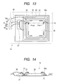
- FIG. 13 is a top view of a semiconductor integrated circuit device according to a fourth embodiment of the invention.
- FIG. 14 is a cross section taken along line A-B of FIG. 13 .
- the virtual reference potential VSSM is supplied via the wiring pattern P 1 ( FIG. 11 ) in the third embodiment, it may be also supplied by using a power supply bus.
- FIG. 13 is a top view of a semiconductor integrated circuit device 1 b
- FIG. 14 is a cross section taken along line A-B of FIG. 13 .
- FIGS. 13 and 14 show a state where a package is formed.
- the semiconductor integrated circuit device 1 b is made by, for example, a QFP (Quad Flat Package), a QFN (Quad Flat Non-Leaded Package), or the like.
- the semiconductor integrated circuit device 1 b is formed as a system-in-package which is the same as that of the semiconductor integrated circuit device 1 a ( FIGS. 10 and 11 ) of the third embodiment provided with the semiconductor chip 26 and the semiconductor chip 27 configuring the low-power drive circuit 9 .
- the semiconductor chip 26 is mounted on a base 31
- the semiconductor chip 27 is mounted on the left side of the semiconductor chip 26 .
- a frame-shaped power supply bus 32 for supplying the power supply voltage VDD is formed on the outer peripheral side of the semiconductor chip 26 .
- a frame-shaped virtual reference potential bus 33 for supplying the virtual reference potential VSSM is formed on the outer peripheral side of the power supply bus 32 .
- a frame-shaped reference potential bus 34 for supplying the reference potential VSS is formed on the outer peripheral side of the semiconductor chip 27 .
- a plurality of leads 35 are formed in the outer peripheries of four sides of the base 31 .
- the two second ground terminals Pvssm provided for the semiconductor chip 26 are coupled to the virtual reference potential bus 33 via bonding wires 36 and 36 a in the shortest distance.
- the virtual reference potential bus 33 is coupled to the output terminal of the semiconductor chip 27 via a bonding wire 37 .
- the power supply bus 32 is coupled to a lead 35 a via a bonding wire 38 .
- a lead 35 b and a bonding wire 39 are assigned as power supply terminals, and the reference potential bus 34 , a lead 35 c , a bonding wire 40 , and the semiconductor chip 27 are assigned as ground terminals.
- the semiconductor chips 26 and 27 , the power supply bus 32 , the virtual reference potential bus 33 , the reference potential bus 34 , the bonding wires 36 , 36 a , 37 to 40 , and the like are sealed with a resin, thereby forming a package.
- the virtual reference potential VSSM can be supplied from the position closest to the second ground terminal Pvssm of the semiconductor chip 26 . Therefore, the virtual reference potential VSSM can be controlled stably.
- the wiring region for the virtual reference potential VSSM in the semiconductor chip 26 can be reduced, and the occupation area of the power supply wiring in the semiconductor chip 26 can be reduced.
- FIG. 15 is a top view showing a configuration example of a semiconductor integrated circuit device according to a fifth embodiment of the invention.
- FIG. 16 is an explanatory diagram showing another configuration example of the semiconductor integrated circuit device according to the fifth embodiment of the invention.
- a semiconductor integrated circuit device 1 c is formed as a package such as a QFP or a QFN in a manner similar to the fourth embodiment except that the low-power drive circuit 9 is formed not by a semiconductor chip but a power-supply IC.
- the semiconductor chip 26 is mounted in the center portion of the base 31 .
- the frame-shaped virtual reference potential bus 33 is formed so as to surround the semiconductor chip 26 .
- the frame-shaped reference potential bus 34 is formed so as to surround the virtual reference potential bus 33 .
- the frame-shaped power supply bus 32 is formed so as to surround the reference potential bus 34 .
- a plurality of electrodes are formed in an array on the top face of the semiconductor chip 26 .
- a plurality of inner leads 67 are formed. The inner leads 67 extend from the package and become outer leads 68 .
- External terminals of the low-power drive circuit 9 formed as a power supply IC are coupled to the virtual reference potential bus 33 , the reference potential bus 34 , and the power supply bus 32 .
- the virtual reference potential bus 33 is coupled to the second ground terminal Pvssm of the semiconductor chip 26 via the bonding wire 39
- the reference potential bus 34 is coupled to the ground terminal Pvss of the semiconductor chip 26 via the bonding wire 40 .
- the power supply bus 32 is coupled to the power supply terminal Pvdd of the semiconductor chip 26 via a bonding wire 41 .
- An inner lead 69 for power supply is coupled to the power supply part of the low-power drive circuit 9 via a bonding wire 42 , so that the power supply voltage VCC is supplied to the low-power drive circuit 9 .
- another electrode part of the semiconductor chip 26 and an arbitrary inner lead 67 are also coupled to each other via a bonding wire.
- the low-power drive circuit 9 as a power supply IC for the virtual reference potential bus 33 , the reference potential bus 34 , and the power supply bus 32 , a space above the buses can be effectively utilized, and the semiconductor integrated circuit device 1 c can be miniaturized.
- the low-power drive circuit 9 as a power supply IC may not be disposed above the buses but may be mounted on the semiconductor chip 26 as shown in FIG. 16 .
- the virtual reference potential VSSM is coupled to the virtual reference potential bus 33 via the bonding wire 42 .
- the semiconductor integrated circuit device 1 c can be further miniaturized.
- FIG. 17 is an explanatory diagram showing a configuration example of a semiconductor integrated circuit device according to a sixth embodiment of the invention.
- the package form is a QFP, QFN, or the like in a manner similar to the foregoing fourth and fifth embodiments.
- the frame-shaped virtual reference potential bus 33 is formed so as to surround the semiconductor chip 26 as shown in FIG. 17 .
- the frame-shaped reference potential bus 34 is formed so as to surround the virtual reference potential bus 33 .
- the frame-shaped power supply bus 32 is formed so as to surround the reference potential bus 34 .
- the plurality of inner leads 67 are formed.
- the low-power drive circuit 9 is disposed in an upper left part of the semiconductor chip 26 .
- electrodes 43 for outputting the virtual reference potential VSSM output from the low-power drive circuit 9 are formed from an upper part to a lower part of the semiconductor chip 26 .
- the electrode 43 is coupled to the virtual reference potential bus 33 via a bonding wire 44 .
- An electrode 45 to which the virtual reference potential VSSM is input is formed below the semiconductor chip 26 .
- the electrode 45 is coupled to the virtual reference potential bus 33 via a bonding wire 46 . Therefore, the virtual reference potential VSSM output from the low-power drive circuit 9 is supplied via the electrode 43 , the bonding wire 44 , the virtual reference potential bus 33 , the electrode 45 , and the bonding wire 46 .
- the virtual reference potential VSS can be efficiently supplied to an arbitrary region which is desired to be controlled in the low-speed mode.
- FIG. 18 is an explanatory diagram showing a configuration example of a semiconductor integrated circuit device according to a seventh embodiment of the invention.
- a frame-shaped virtual reference potential bus 33 a is formed so as to surround the semiconductor chip 26 .
- a frame-shaped virtual reference potential bus 33 b is formed so as to surround the virtual reference potential bus 33 a .
- a frame-shaped virtual reference potential bus 33 c is formed so as to surround the virtual reference potential bus 33 b.
- the virtual reference potential bus 33 a supplies a virtual reference potential VSSM 1 to the region 48 .
- the virtual reference potential bus 33 b supplies a virtual reference potential VSSM 2 to the region 47 .
- the virtual reference bus 33 c supplies a virtual reference potential VSSM 3 to the region 49 .
- the power switches 11 are formed on both sides of each of the regions 47 to 49 .
- the virtual reference potentials VSSM 1 to VSSM 3 are supplied from the outside like in the case of FIG. 9 .
- power is supplied to the virtual reference potential buses 33 a to 33 c from the inner leads 37 b to 37 d via bonding wires 50 to 52 .
- the levels of the virtual reference potentials VSSM 1 to VSSM 3 can be easily arbitrarily controlled.
- FIG. 19 is an explanatory diagram showing an example of power feeding wires used for virtual reference potentials of a semiconductor chip provided for a semiconductor device according to an eighth embodiment of the invention.
- FIG. 19 is an explanatory diagram showing a layout example of highest-order metal wires of the semiconductor chip 26 .
- the wires 53 are wires for the reference potential VSS, and the wires 54 are wires for the power supply voltage VDD.
- wires 55 as wires for the virtual reference potential VSSM 1 are formed at equal intervals from the left side to the right side of the region 47 .
- wires 56 as wires for the virtual reference potential VSSM 2 are formed at equal intervals from the left side to the right side of the region 48 .
- wires 57 as wires for the virtual reference potential VSSM 3 are formed at equal intervals from the left side to the right side of the region 49 .
- FIG. 20 is an explanatory diagram showing a formation example of outer leads provided for a semiconductor integrated circuit device according to a ninth embodiment of the invention.
- FIG. 21 is a cross section of the semiconductor integrated circuit device according to the ninth embodiment of the invention.
- the semiconductor chip 26 is mounted in the center portion of the base 31 .
- the frame-shaped virtual reference potential bus 33 is formed so as to surround the semiconductor chip 26 .
- the frame-shaped power supply bus 32 is formed so as to surround the virtual reference potential bus 33 .
- the frame-shaped reference potential bus 34 is formed on the outer peripheral side of the power supply bus 32 .
- a plurality of electrodes are formed in the peripheral portion of the semiconductor chip 26 .
- Arbitrary electrodes and the virtual reference potential bus 33 , the power supply bus 32 , and the reference potential bus 34 formed in the base 31 near the outer periphery of the semiconductor chip 26 are coupled to each other via bonding wires 58 .
- the other electrodes of the semiconductor chip 26 are coupled to via the leads 35 and bonding wires 70 provided in the periphery of the reference potential bus 34 .
- Four corners of the reference potential bus 34 extend to form leads 59 to 62 .
- the base 31 , the semiconductor chip 26 , the virtual reference potential bus 33 , the power supply bus 32 , the reference potential bus 34 , the lead 35 , the leads 59 to 62 , the bonding wires 58 and 70 , and the like are sealed with the sealing resin 30 , thereby forming a package.
- the virtual reference potential bus 33 , the power supply bus 32 , and the reference potential bus 34 are adhered by, for example, a tape, a heat splitter adhesive, or the like.
- FIG. 22 is an explanatory diagram showing an example of a virtual reference potential bus provided for a semiconductor integrated circuit device according to a tenth embodiment of the invention.
- the frame-shaped power supply bus 32 is formed so as to surround the semiconductor chip 26 .
- the frame-shaped reference potential bus 34 is formed on the outer peripheral side of the power supply bus 32 .
- a linear-shaped virtual reference potential bus 33 a is formed between the upper side of the power supply bus 32 and the upper side of the reference potential bus 34 . Between the right side of the power supply bus 32 and the right side of the reference potential bus 34 , a linear-shaped virtual reference potential bus 33 b is formed. Between the lower side of the power supply bus 32 and the lower side of the reference potential bus 34 , a linear-shaped virtual reference potential bus 33 c is formed. Further, between the left side of the power supply bus 32 and the left side of the reference potential bus 34 , a linear-shaped virtual reference potential bus 33 d is formed.
- the virtual reference potential buses 33 a to 33 d supply the virtual reference potentials VSSM 1 to VSSM 4 to the four second ground terminals Pvssm provided for the semiconductor chip 26 via bonding wires 63 to 66 .
- the present invention is suitably applied to a semiconductor integrated circuit device in which the low-power consumption control is performed every power supply region in which one or more function modules are disposed.
Landscapes
- Engineering & Computer Science (AREA)
- General Engineering & Computer Science (AREA)
- Physics & Mathematics (AREA)
- Theoretical Computer Science (AREA)
- Computer Hardware Design (AREA)
- General Physics & Mathematics (AREA)
- Computing Systems (AREA)
- Power Engineering (AREA)
- Microelectronics & Electronic Packaging (AREA)
- Condensed Matter Physics & Semiconductors (AREA)
- Mathematical Physics (AREA)
- Semiconductor Integrated Circuits (AREA)
- Logic Circuits (AREA)
Priority Applications (2)
| Application Number | Priority Date | Filing Date | Title |
|---|---|---|---|
| US13/244,553 US8253481B2 (en) | 2008-11-14 | 2011-09-25 | Semiconductor integrated circuit device |
| US13/562,157 US8421527B2 (en) | 2008-11-14 | 2012-07-30 | Semiconductor integrated circuit device |
Applications Claiming Priority (2)
| Application Number | Priority Date | Filing Date | Title |
|---|---|---|---|
| JP2008-291929 | 2008-11-14 | ||
| JP2008291929A JP5374120B2 (ja) | 2008-11-14 | 2008-11-14 | 半導体集積回路装置 |
Related Child Applications (1)
| Application Number | Title | Priority Date | Filing Date |
|---|---|---|---|
| US13/244,553 Continuation US8253481B2 (en) | 2008-11-14 | 2011-09-25 | Semiconductor integrated circuit device |
Publications (2)
| Publication Number | Publication Date |
|---|---|
| US20100123515A1 US20100123515A1 (en) | 2010-05-20 |
| US8044709B2 true US8044709B2 (en) | 2011-10-25 |
Family
ID=42171524
Family Applications (3)
| Application Number | Title | Priority Date | Filing Date |
|---|---|---|---|
| US12/608,105 Expired - Fee Related US8044709B2 (en) | 2008-11-14 | 2009-10-29 | Semiconductor integrated circuit device |
| US13/244,553 Expired - Fee Related US8253481B2 (en) | 2008-11-14 | 2011-09-25 | Semiconductor integrated circuit device |
| US13/562,157 Active US8421527B2 (en) | 2008-11-14 | 2012-07-30 | Semiconductor integrated circuit device |
Family Applications After (2)
| Application Number | Title | Priority Date | Filing Date |
|---|---|---|---|
| US13/244,553 Expired - Fee Related US8253481B2 (en) | 2008-11-14 | 2011-09-25 | Semiconductor integrated circuit device |
| US13/562,157 Active US8421527B2 (en) | 2008-11-14 | 2012-07-30 | Semiconductor integrated circuit device |
Country Status (3)
| Country | Link |
|---|---|
| US (3) | US8044709B2 (ja) |
| JP (1) | JP5374120B2 (ja) |
| CN (1) | CN101739117B (ja) |
Cited By (4)
| Publication number | Priority date | Publication date | Assignee | Title |
|---|---|---|---|---|
| US8253481B2 (en) * | 2008-11-14 | 2012-08-28 | Renesas Electronics Corporation | Semiconductor integrated circuit device |
| US20130173077A1 (en) * | 2011-12-29 | 2013-07-04 | Lsi Corporation | Power switch having series-connected switching stages |
| US20150179234A1 (en) * | 2013-12-25 | 2015-06-25 | Kabushiki Kaisha Toshiba | Semiconductor system and power source chip |
| US9653131B1 (en) * | 2016-02-12 | 2017-05-16 | Micron Technology, Inc. | Apparatuses and methods for voltage level control |
Families Citing this family (18)
| Publication number | Priority date | Publication date | Assignee | Title |
|---|---|---|---|---|
| US8319548B2 (en) * | 2009-02-18 | 2012-11-27 | Freescale Semiconductor, Inc. | Integrated circuit having low power mode voltage regulator |
| US20100283445A1 (en) * | 2009-02-18 | 2010-11-11 | Freescale Semiconductor, Inc. | Integrated circuit having low power mode voltage regulator |
| US8400819B2 (en) * | 2010-02-26 | 2013-03-19 | Freescale Semiconductor, Inc. | Integrated circuit having variable memory array power supply voltage |
| US8489906B2 (en) * | 2010-05-25 | 2013-07-16 | Freescale Semiconductor, Inc. | Data processor having multiple low power modes |
| JP5498896B2 (ja) * | 2010-08-26 | 2014-05-21 | ルネサスエレクトロニクス株式会社 | 半導体チップ |
| US8476966B2 (en) * | 2010-10-05 | 2013-07-02 | International Business Machines Corporation | On-die voltage regulation using p-FET header devices with a feedback control loop |
| US9035629B2 (en) | 2011-04-29 | 2015-05-19 | Freescale Semiconductor, Inc. | Voltage regulator with different inverting gain stages |
| JP6065480B2 (ja) * | 2012-09-14 | 2017-01-25 | 株式会社リコー | 半導体集積回路および電子回路 |
| FR2999832A1 (fr) * | 2012-12-14 | 2014-06-20 | St Microelectronics Sa | Procede et dispositif de gestion d'une mise sous tension d'un domaine d'un circuit electronique |
| US9766678B2 (en) | 2013-02-04 | 2017-09-19 | Intel Corporation | Multiple voltage identification (VID) power architecture, a digital synthesizable low dropout regulator, and apparatus for improving reliability of power gates |
| US8766707B1 (en) * | 2013-03-15 | 2014-07-01 | Seagate Technology Llc | Integrated always on power island for low power mode operation |
| JP6225541B2 (ja) * | 2013-07-29 | 2017-11-08 | 富士通株式会社 | 半導体装置 |
| US20150028941A1 (en) * | 2013-07-29 | 2015-01-29 | Texas Instruments Incorporated | Controlled power switch chain sequencing for both power up and power down of a power domain |
| KR102021572B1 (ko) * | 2013-10-01 | 2019-09-16 | 에스케이하이닉스 주식회사 | 반도체 장치 |
| KR20150140047A (ko) * | 2014-06-05 | 2015-12-15 | 삼성전기주식회사 | 적분 회로, 접촉 감지 장치 및 터치스크린 장치 |
| CN104977961B (zh) * | 2015-07-08 | 2016-06-22 | 江阴市飞凌科技有限公司 | 低功耗低电流分享方法 |
| US10659045B2 (en) * | 2017-06-27 | 2020-05-19 | Silicon Laboratories Inc. | Apparatus with electronic circuitry having reduced leakage current and associated methods |
| JP7160105B2 (ja) * | 2018-09-28 | 2022-10-25 | 株式会社ソシオネクスト | 半導体装置 |
Citations (14)
| Publication number | Priority date | Publication date | Assignee | Title |
|---|---|---|---|---|
| US5583457A (en) * | 1992-04-14 | 1996-12-10 | Hitachi, Ltd. | Semiconductor integrated circuit device having power reduction mechanism |
| US5687123A (en) * | 1993-10-14 | 1997-11-11 | Mitsubishi Denki Kabushiki Kaisha | Semiconductor memory device |
| JPH10125878A (ja) | 1996-10-21 | 1998-05-15 | Nippon Telegr & Teleph Corp <Ntt> | ゲートアレイ |
| US6140864A (en) * | 1996-09-12 | 2000-10-31 | Matsushita Electric Industrial Co., Ltd. | Circuit for controlling leakage current in large scale integrated circuits |
| US6292015B1 (en) * | 1998-05-26 | 2001-09-18 | Mitsubishi Denki Kabushiki Kaisha | Semiconductor integrated circuit device including logic gate that attains reduction of power consumption and high-speed operation |
| US6313695B1 (en) * | 1998-11-17 | 2001-11-06 | Mitsubishi Denki Kabushiki Kaisha | Semiconductor circuit device having hierarchical power supply structure |
| US6411149B1 (en) * | 1996-07-30 | 2002-06-25 | Mitsubishi Denki Kabushiki Kaisha | Semiconductor integrated circuit device operable with low power consumption at low power supply voltage |
| US6888395B2 (en) * | 2002-01-28 | 2005-05-03 | Renesas Technology Corp. | Semiconductor integrated circuit device |
| US7042245B2 (en) * | 2002-10-25 | 2006-05-09 | Renesas Technology Corp. | Low power consumption MIS semiconductor device |
| US7251170B2 (en) * | 2005-09-05 | 2007-07-31 | Hynix Semiconductor Inc. | Peripheral voltage generator |
| US20080116956A1 (en) * | 2006-11-20 | 2008-05-22 | Elpida Memory, Inc. | Semiconductor device operating in an active mode and a standby mode |
| US7479801B2 (en) * | 2004-10-28 | 2009-01-20 | International Business Machines Corporation | Power gating techniques able to have data retention and variability immunity properties |
| US7639068B2 (en) * | 2001-11-30 | 2009-12-29 | Renesas Technology Corp. | Voltage supply with low power and leakage current |
| US20100109764A1 (en) * | 2008-10-28 | 2010-05-06 | Lutz Dathe | Circuit, an adjusting method, and use of a control loop |
Family Cites Families (21)
| Publication number | Priority date | Publication date | Assignee | Title |
|---|---|---|---|---|
| JP4049758B2 (ja) * | 1994-06-02 | 2008-02-20 | 株式会社ルネサステクノロジ | 半導体記憶装置 |
| JP3645593B2 (ja) * | 1994-09-09 | 2005-05-11 | 株式会社ルネサステクノロジ | 半導体集積回路装置 |
| JP5041631B2 (ja) * | 2001-06-15 | 2012-10-03 | ルネサスエレクトロニクス株式会社 | 半導体記憶装置 |
| JP4001229B2 (ja) * | 2002-06-10 | 2007-10-31 | シャープ株式会社 | 半導体集積回路および半導体モジュール |
| KR100594142B1 (ko) * | 2003-12-08 | 2006-06-28 | 삼성전자주식회사 | 분리된 전원 링을 가지는 저전력 반도체 칩과 그 제조 및제어방법 |
| JP2005268694A (ja) * | 2004-03-22 | 2005-09-29 | Sony Corp | 半導体集積回路およびその作製方法 |
| JP4764086B2 (ja) * | 2005-07-27 | 2011-08-31 | パナソニック株式会社 | 半導体集積回路装置 |
| US8067976B2 (en) * | 2005-08-02 | 2011-11-29 | Panasonic Corporation | Semiconductor integrated circuit |
| US20070069807A1 (en) * | 2005-09-23 | 2007-03-29 | Intel Corporation | Voltage regulation having varying reference during operation |
| US7265605B1 (en) * | 2005-10-18 | 2007-09-04 | Xilinx, Inc. | Supply regulator for memory cells with suspend mode capability for low power applications |
| JP5105462B2 (ja) * | 2005-12-27 | 2012-12-26 | ルネサスエレクトロニクス株式会社 | 半導体集積回路 |
| KR100735677B1 (ko) * | 2005-12-28 | 2007-07-04 | 삼성전자주식회사 | 스탠바이 전류 저감 회로 및 이를 구비한 반도체 메모리장치 |
| US7911855B2 (en) * | 2006-02-24 | 2011-03-22 | Renesas Technology Corp. | Semiconductor device with voltage interconnections |
| EP3694092A1 (en) * | 2006-05-10 | 2020-08-12 | QUALCOMM Incorporated | System and method of power distribution control of an integrated circuit |
| JP5077986B2 (ja) * | 2006-08-31 | 2012-11-21 | ルネサスエレクトロニクス株式会社 | 半導体集積回路 |
| JP2008218722A (ja) * | 2007-03-05 | 2008-09-18 | Renesas Technology Corp | 半導体集積回路装置 |
| US7705575B2 (en) * | 2008-04-10 | 2010-04-27 | Spectralinear, Inc. | Standby regulator |
| US7705627B1 (en) * | 2008-10-17 | 2010-04-27 | Samsung Electronics Co., Ltd. | Semiconductor device using power gating |
| JP5374120B2 (ja) * | 2008-11-14 | 2013-12-25 | ルネサスエレクトロニクス株式会社 | 半導体集積回路装置 |
| US7760009B2 (en) * | 2008-12-04 | 2010-07-20 | Taiwan Semiconductor Manufacturing Company, Ltd. | Power-down circuit with self-biased compensation circuit |
| US7825720B2 (en) * | 2009-02-18 | 2010-11-02 | Freescale Semiconductor, Inc. | Circuit for a low power mode |
-
2008
- 2008-11-14 JP JP2008291929A patent/JP5374120B2/ja not_active Expired - Fee Related
-
2009
- 2009-10-29 US US12/608,105 patent/US8044709B2/en not_active Expired - Fee Related
- 2009-11-13 CN CN200910222437.9A patent/CN101739117B/zh not_active Expired - Fee Related
-
2011
- 2011-09-25 US US13/244,553 patent/US8253481B2/en not_active Expired - Fee Related
-
2012
- 2012-07-30 US US13/562,157 patent/US8421527B2/en active Active
Patent Citations (14)
| Publication number | Priority date | Publication date | Assignee | Title |
|---|---|---|---|---|
| US5583457A (en) * | 1992-04-14 | 1996-12-10 | Hitachi, Ltd. | Semiconductor integrated circuit device having power reduction mechanism |
| US5687123A (en) * | 1993-10-14 | 1997-11-11 | Mitsubishi Denki Kabushiki Kaisha | Semiconductor memory device |
| US6411149B1 (en) * | 1996-07-30 | 2002-06-25 | Mitsubishi Denki Kabushiki Kaisha | Semiconductor integrated circuit device operable with low power consumption at low power supply voltage |
| US6140864A (en) * | 1996-09-12 | 2000-10-31 | Matsushita Electric Industrial Co., Ltd. | Circuit for controlling leakage current in large scale integrated circuits |
| JPH10125878A (ja) | 1996-10-21 | 1998-05-15 | Nippon Telegr & Teleph Corp <Ntt> | ゲートアレイ |
| US6292015B1 (en) * | 1998-05-26 | 2001-09-18 | Mitsubishi Denki Kabushiki Kaisha | Semiconductor integrated circuit device including logic gate that attains reduction of power consumption and high-speed operation |
| US6313695B1 (en) * | 1998-11-17 | 2001-11-06 | Mitsubishi Denki Kabushiki Kaisha | Semiconductor circuit device having hierarchical power supply structure |
| US7639068B2 (en) * | 2001-11-30 | 2009-12-29 | Renesas Technology Corp. | Voltage supply with low power and leakage current |
| US6888395B2 (en) * | 2002-01-28 | 2005-05-03 | Renesas Technology Corp. | Semiconductor integrated circuit device |
| US7042245B2 (en) * | 2002-10-25 | 2006-05-09 | Renesas Technology Corp. | Low power consumption MIS semiconductor device |
| US7479801B2 (en) * | 2004-10-28 | 2009-01-20 | International Business Machines Corporation | Power gating techniques able to have data retention and variability immunity properties |
| US7251170B2 (en) * | 2005-09-05 | 2007-07-31 | Hynix Semiconductor Inc. | Peripheral voltage generator |
| US20080116956A1 (en) * | 2006-11-20 | 2008-05-22 | Elpida Memory, Inc. | Semiconductor device operating in an active mode and a standby mode |
| US20100109764A1 (en) * | 2008-10-28 | 2010-05-06 | Lutz Dathe | Circuit, an adjusting method, and use of a control loop |
Cited By (6)
| Publication number | Priority date | Publication date | Assignee | Title |
|---|---|---|---|---|
| US8253481B2 (en) * | 2008-11-14 | 2012-08-28 | Renesas Electronics Corporation | Semiconductor integrated circuit device |
| US8421527B2 (en) * | 2008-11-14 | 2013-04-16 | Renesas Electronics Corporation | Semiconductor integrated circuit device |
| US20130173077A1 (en) * | 2011-12-29 | 2013-07-04 | Lsi Corporation | Power switch having series-connected switching stages |
| US20150179234A1 (en) * | 2013-12-25 | 2015-06-25 | Kabushiki Kaisha Toshiba | Semiconductor system and power source chip |
| US9653131B1 (en) * | 2016-02-12 | 2017-05-16 | Micron Technology, Inc. | Apparatuses and methods for voltage level control |
| US10242724B2 (en) | 2016-02-12 | 2019-03-26 | Micron Technology, Inc. | Apparatuses and methods for voltage level control |
Also Published As
| Publication number | Publication date |
|---|---|
| CN101739117A (zh) | 2010-06-16 |
| US8421527B2 (en) | 2013-04-16 |
| CN101739117B (zh) | 2014-06-18 |
| US20120013382A1 (en) | 2012-01-19 |
| US20120293247A1 (en) | 2012-11-22 |
| US20100123515A1 (en) | 2010-05-20 |
| US8253481B2 (en) | 2012-08-28 |
| JP2010118590A (ja) | 2010-05-27 |
| JP5374120B2 (ja) | 2013-12-25 |
Similar Documents
| Publication | Publication Date | Title |
|---|---|---|
| US8044709B2 (en) | Semiconductor integrated circuit device | |
| US6683767B2 (en) | Semiconductor integrated circuit | |
| US9406648B2 (en) | Power supply arrangement for semiconductor device | |
| US20070194841A1 (en) | Semiconductor integrated circuit device | |
| US20090057417A1 (en) | Ic card | |
| CN101207115B (zh) | 半导体集成电路 | |
| US20080001656A1 (en) | Semiconductor integrated circuit | |
| US6847512B2 (en) | Electrostatic breakdown prevention circuit for semiconductor device | |
| US6653693B1 (en) | Semiconductor integrated circuit device | |
| US20040130016A1 (en) | Semiconductor device and different levels of signal processing systems using the same | |
| US8704410B2 (en) | Semiconductor device | |
| JP2005175489A (ja) | 分離された電源リングを有する低電力半導体チップとその製造及び制御方法 | |
| US20090284287A1 (en) | Output buffer circuit and integrated circuit | |
| US6822921B2 (en) | Semiconductor device having semiconductor memory | |
| US7212065B2 (en) | Semiconductor integrated circuit device capable of restraining variations in the power supply potential | |
| JP5374285B2 (ja) | 半導体装置及びその制御方法 | |
| JPH07235608A (ja) | 半導体集積回路装置 | |
| JP2010245413A (ja) | 半導体集積回路装置 | |
| JP2003318263A (ja) | 半導体装置 | |
| KR20090087334A (ko) | 에스씨알 회로를 이용한 정전기 방전 장치 | |
| US20110187446A1 (en) | Semiconductor device | |
| JP2000183714A (ja) | 半導体集積回路 | |
| JPH04163958A (ja) | 半導体装置 | |
| JPH10322904A (ja) | 電源制御回路 | |
| JP2002151650A (ja) | 半導体装置 |
Legal Events
| Date | Code | Title | Description |
|---|---|---|---|
| AS | Assignment |
Owner name: RENESAS TECHNOLOGY CORP.,JAPAN Free format text: ASSIGNMENT OF ASSIGNORS INTEREST;ASSIGNORS:SASAKI, TOSHIO;FUKUOKA, KAZUKI;MORI, RYO;AND OTHERS;SIGNING DATES FROM 20090903 TO 20090914;REEL/FRAME:023442/0756 Owner name: RENESAS TECHNOLOGY CORP., JAPAN Free format text: ASSIGNMENT OF ASSIGNORS INTEREST;ASSIGNORS:SASAKI, TOSHIO;FUKUOKA, KAZUKI;MORI, RYO;AND OTHERS;SIGNING DATES FROM 20090903 TO 20090914;REEL/FRAME:023442/0756 |
|
| AS | Assignment |
Owner name: RENESAS ELECTRONICS CORPORATION, JAPAN Free format text: CHANGE OF NAME;ASSIGNOR:NEC ELECTRONICS CORPORATION;REEL/FRAME:024864/0635 Effective date: 20100401 Owner name: NEC ELECTRONICS CORPORATION, JAPAN Free format text: MERGER;ASSIGNOR:RENESAS TECHNOLOGY CORP.;REEL/FRAME:024879/0190 Effective date: 20100401 |
|
| STCF | Information on status: patent grant |
Free format text: PATENTED CASE |
|
| FEPP | Fee payment procedure |
Free format text: PAYOR NUMBER ASSIGNED (ORIGINAL EVENT CODE: ASPN); ENTITY STATUS OF PATENT OWNER: LARGE ENTITY |
|
| FPAY | Fee payment |
Year of fee payment: 4 |
|
| AS | Assignment |
Owner name: RENESAS ELECTRONICS CORPORATION, JAPAN Free format text: CHANGE OF ADDRESS;ASSIGNOR:RENESAS ELECTRONICS CORPORATION;REEL/FRAME:044928/0001 Effective date: 20150806 |
|
| FEPP | Fee payment procedure |
Free format text: MAINTENANCE FEE REMINDER MAILED (ORIGINAL EVENT CODE: REM.); ENTITY STATUS OF PATENT OWNER: LARGE ENTITY |
|
| LAPS | Lapse for failure to pay maintenance fees |
Free format text: PATENT EXPIRED FOR FAILURE TO PAY MAINTENANCE FEES (ORIGINAL EVENT CODE: EXP.); ENTITY STATUS OF PATENT OWNER: LARGE ENTITY |
|
| STCH | Information on status: patent discontinuation |
Free format text: PATENT EXPIRED DUE TO NONPAYMENT OF MAINTENANCE FEES UNDER 37 CFR 1.362 |
|
| FP | Lapsed due to failure to pay maintenance fee |
Effective date: 20191025 |